epitaxy: application to polarized emitters aaron moy and brian hertog svt associates, eden prairie,...
TRANSCRIPT

Epitaxy: Application to Polarized Emitters
Aaron Moy and Brian HertogSVT Associates, Eden Prairie, Minnesota
Acknowledgements:US Dept. of Energy SBIR Phase I and II Grant
contract #DE-FG02-01ER83332
in collaboration with SLAC Polarized Photocathode Research Collaboration (PPRC):
A. Brachmann, J. Clendenin, E. Garwin, S. Harvey,
R. Kirby, D.-A. Luh, T. Maruyama, R. Prepost, and C. Prescott

Outline
• Strained Layer Semiconductor for Polarized Electron Source • Epitaxial Crystal Growth
• Methods of III-V Epitaxy• Metal organic chemical vapor deposition (MOCVD)• Molecular beam epitaxy (MBE)• Gas source molecular beam epitaxy (GSMBE)
• Growth of Photocathodes Using GSMBE
• Characterization of Material
Polarized Electron Emitters
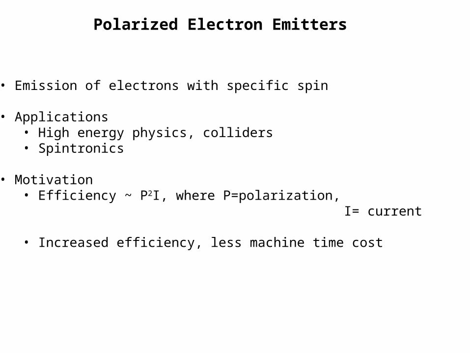
• Emission of electrons with specific spin • Applications
• High energy physics, colliders• Spintronics
• Motivation• Efficiency ~ P2I, where P=polarization, I= current
• Increased efficiency, less machine time cost

Strained Layer Polarized Emitters
• Photocathode emission
• Circularly polarized light
• Unstrained GaAs
• 50% max polarization
• Compressively strained GaAs
• lattice constant < 5.65 Å
• valence band splitting
• 3/2 1/2 transition favored
• 100% max polarization
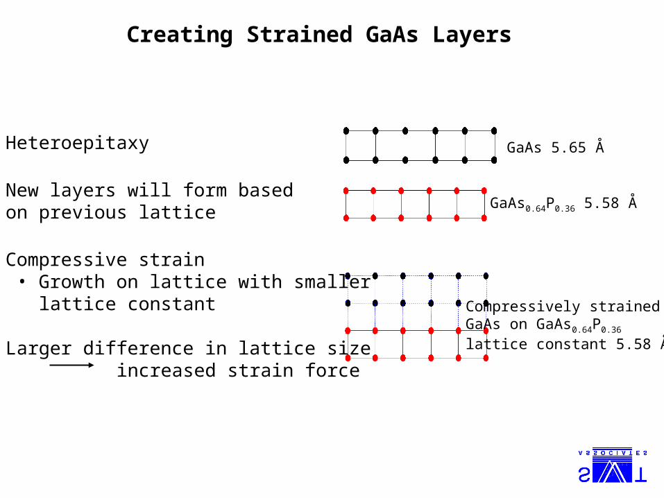
Creating Strained GaAs Layers
• Heteroepitaxy
• New layers will form based on previous lattice
• Compressive strain• Growth on lattice with smaller lattice constant
• Larger difference in lattice size increased strain force
GaAs 5.65 Å
GaAs0.64P0.36 5.58 Å
Compressively strainedGaAs on GaAs0.64P0.36
lattice constant 5.58 Å
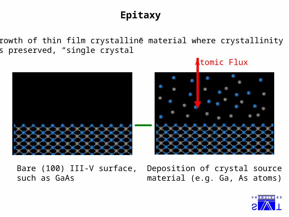
Epitaxy
Bare (100) III-V surface,such as GaAs
Deposition of crystal sourcematerial (e.g. Ga, As atoms)
Growth of thin film crystalline material where crystallinityis preserved, “single crystal”
Atomic Flux
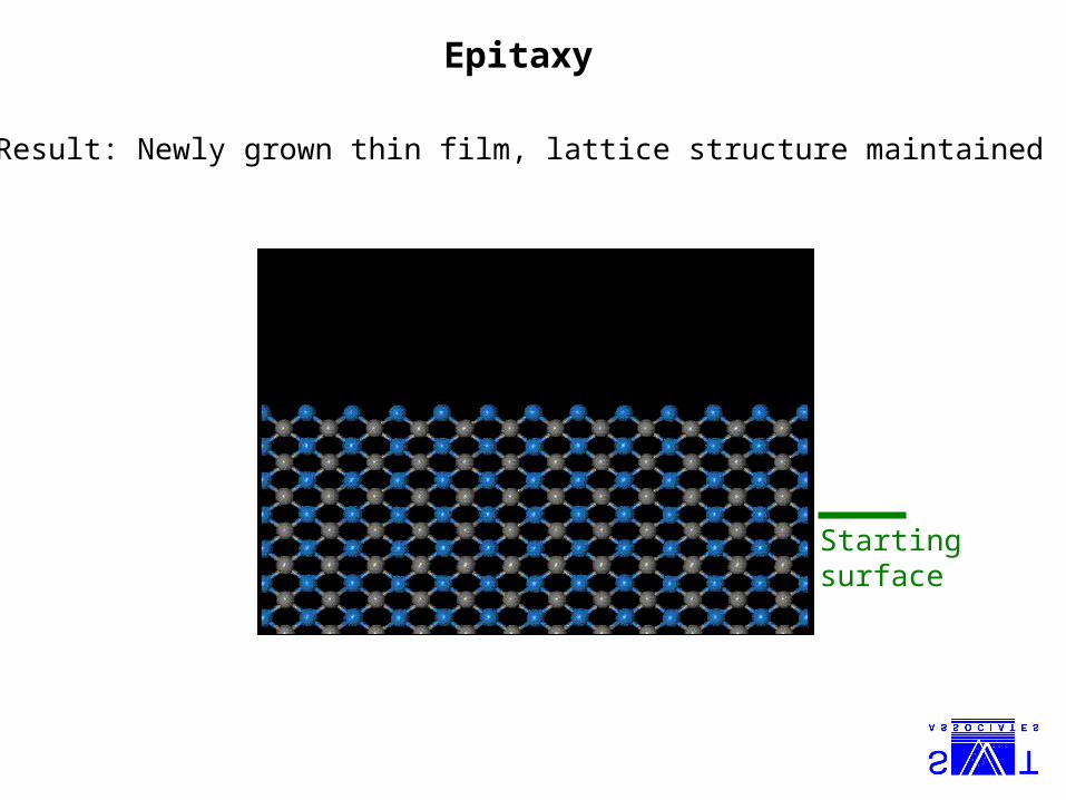
Epitaxy
Result: Newly grown thin film, lattice structure maintained
Starting surface

Epitaxy
Advantages of epitaxy-
• Improved crystallinity
• Reduced defects
• Higher purity
• Precise control of thickness
• Precise control alloy composition
• “Lattice matched” compounds
• Abrupt or graded interfaces
• Ability to engineer unique device structures
• Nanostructures
• Superlattices
• Strained layers
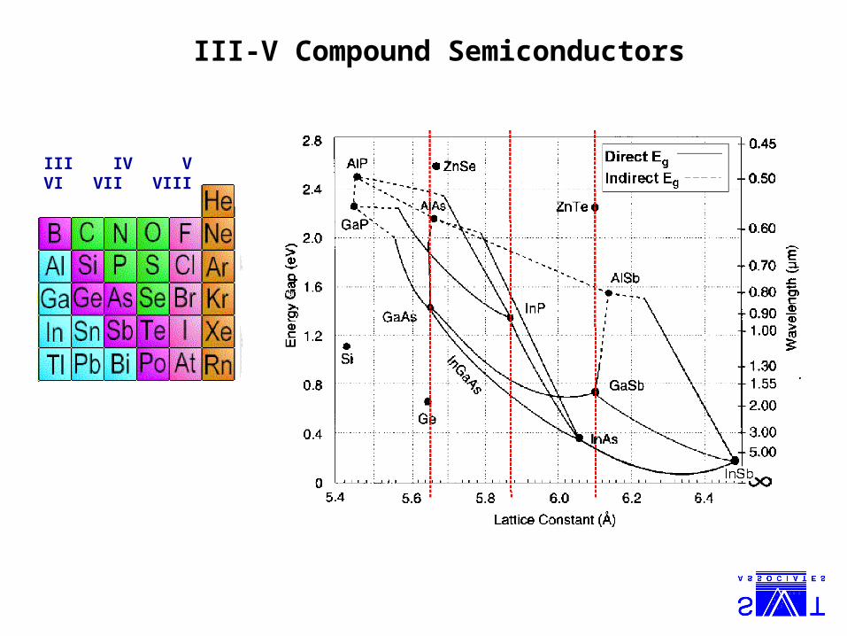
III-V Compound Semiconductors
III IV V VI VII VIII
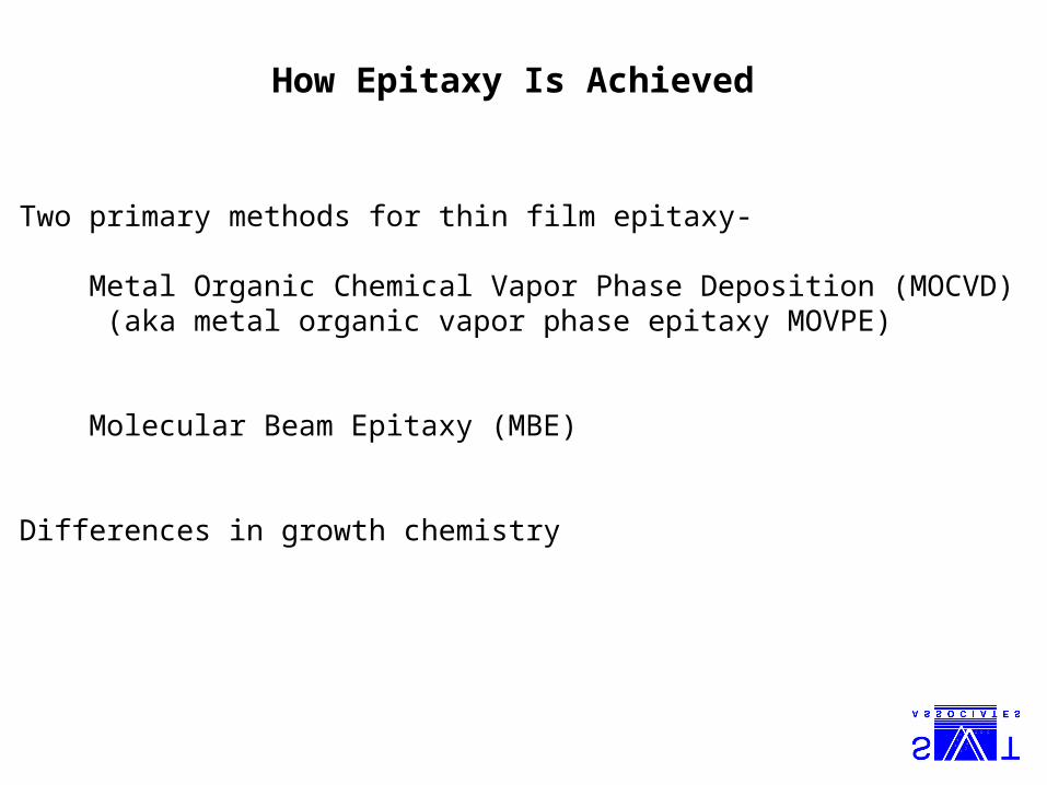
How Epitaxy Is Achieved
• Two primary methods for thin film epitaxy-
Metal Organic Chemical Vapor Phase Deposition (MOCVD) (aka metal organic vapor phase epitaxy MOVPE)
Molecular Beam Epitaxy (MBE)
• Differences in growth chemistry

Metal Organic Chemical Vapor Phase Deposition
• Growth in “reactor”
• Pressure 10s-100s of torr
• Metal organic group III source material
• Trimethyl Gallium Ga(CH3)3
• Trimethyl Indium In(CH3)3
• MO vapor transported H2 carrier gas
• Hydride group V source gas
• Arsine AsH3
• Phosphine PH3
• Thermal cracking at growth surface
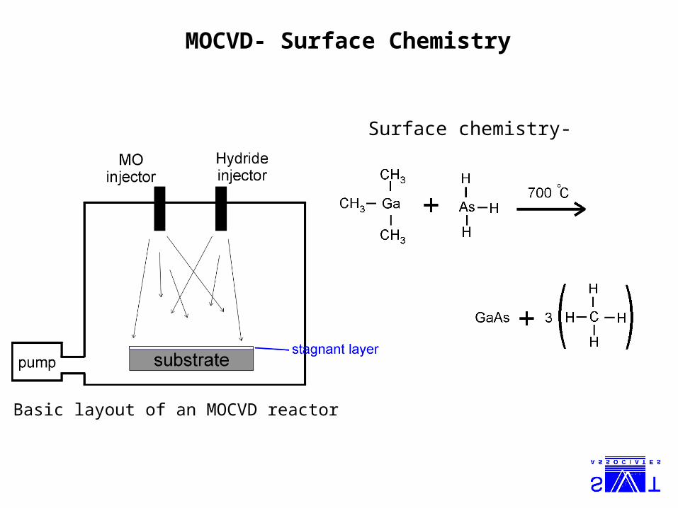
MOCVD- Surface Chemistry
Basic layout of an MOCVD reactor
Surface chemistry-

MOCVD- Gas Handling System
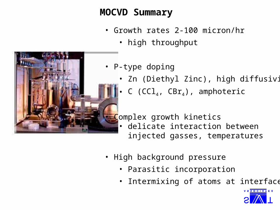
MOCVD Summary
• Growth rates 2-100 micron/hr
• high throughput
• P-type doping
• Zn (Diethyl Zinc), high diffusivity
• C (CCl4, CBr4), amphoteric
• Complex growth kinetics• delicate interaction between injected gasses, temperatures
• High background pressure
• Parasitic incorporation
• Intermixing of atoms at interfaces

Molecular Beam Epitaxy (MBE)
• Growth in high vacuum chamber
• Ultimate vacuum < 10-10 torr
• Pressure during growth < 10-6 torr
• Elemental source material
• High purity Ga, In, As (99.9999%)
• Sources individually evaporated in high temperature cells
• In situ monitoring, calibration
• Probing of surface structure during growth
• Real time feedback of growth rate

Molecular Beam Epitaxy
Growth Apparatus

MBE- In Situ Surface Analysis
• Reflection High Energy Electron Diffraction (RHEED)
• High energy (5-10 keV) electron beam
• Shallow angle of incidence
• Beam reconstruction on phosphor screen
RHEED image of GaAs (100) surface
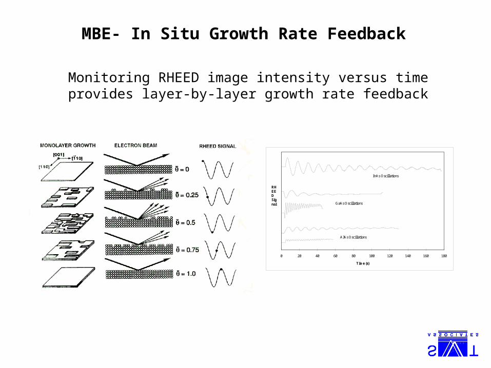
0 20 40 60 80 100 120 140 160 180
Time (s)
RHEEDSignal GaAs Oscillations
AlAs Oscillations
InAs Oscillations
MBE- In Situ Growth Rate Feedback
Monitoring RHEED image intensity versus timeprovides layer-by-layer growth rate feedback

MBE- Summary
• Ultra high vacuum, high purity layers
• No chemical byproducts created at growth surface
• High uniformity (< 1% deviation)
• Growth rates 0.1-10 micron/hr
• High control of composition
• In situ monitoring and feedback
• Mature production technology
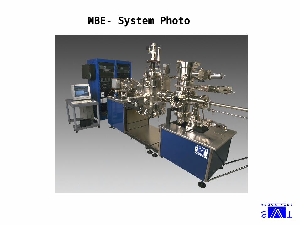
MBE- System Photo
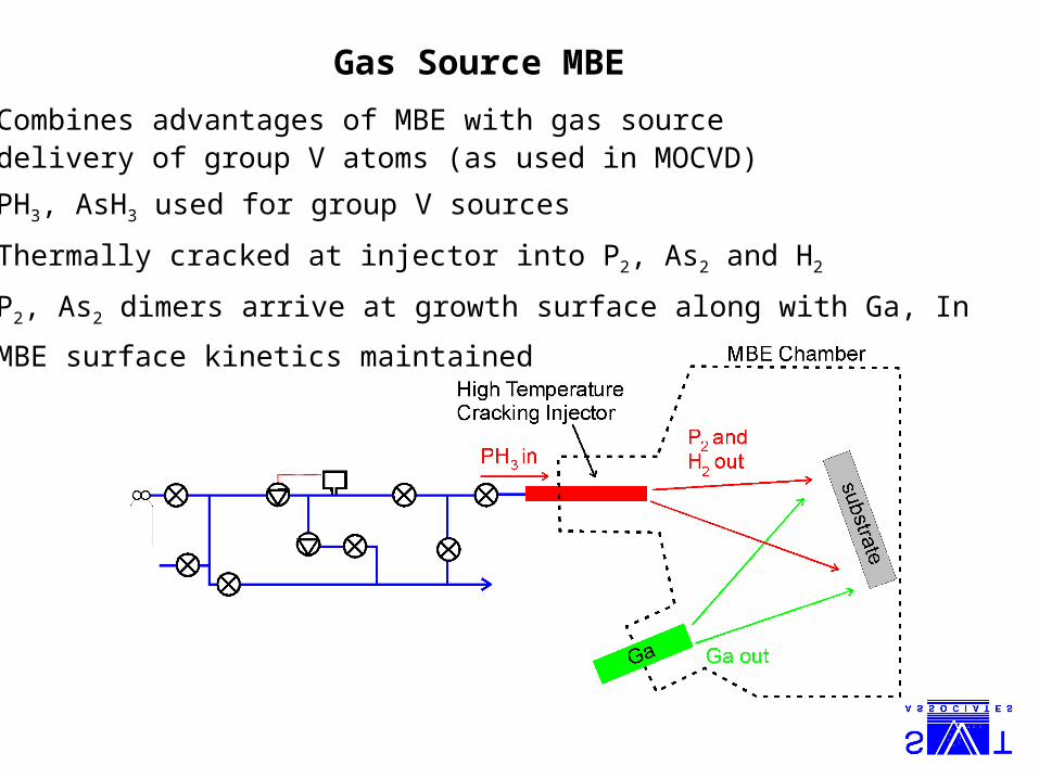
Gas Source MBE
• Combines advantages of MBE with gas source delivery of group V atoms (as used in MOCVD)
• PH3, AsH3 used for group V sources
• Thermally cracked at injector into P2, As2 and H2
• P2, As2 dimers arrive at growth surface along with Ga, In
• MBE surface kinetics maintained

Gas Source MBE
• Advantages of GSMBE
• PH3 a more mature method for phosphorus MBE growth
• Improved dynamic range of switching state
• As, P molecules travel around shutter in solid source MBE
• Control of P, As flux by adjustment of gas flow
• Can replenish group V source material without breaking vacuum
• Disadvantages
• Requires gas handling system
• Requires extra vacuum pumping to remove hydrogen
• Arsine and Phosphine highly toxic

Limits to Strained Layers: Critical Thickness
• Strain forces increase with thickness
• Strain reaches threshold, lattice relaxes
• “Critical Thickness” • Layer thickness where relaxation occurs• Relaxed lattice- bulk crystal state• Thickness inversely proportional to strain (difference in lattice constant)
• Misfit dislocations created• Scattering, absorption of photons• Non-uniformities
GaAs on GaAsPCritical Thickness

Photocathode Polarized Emitters
• Device Considerations
• Strained GaAs layer• Highly p-type doped• Thick to provide enough emission current
• Structure Growth• Uniform• Excellent crystallinity
• Substrate for epitaxy• High quality• Robust

Strained Superlattice Photocathode
• Strained GaAs on GaAsxP1-x
• Multiple GaAs layers sandwiched by GaAsxP1-x
• Each GaAs layer below critical thickness• Multiple GaAs layers to provide thick overall active volume for electron emission
• Superlattice- repetition of thin layers
• GSMBE for epitaxy
• Thin layers (< 50 Å)
• Utilizes phosphorus
• Abrupt, uniform interfaces

Strained GaAs
GaAsP
Strained GaAs
GaAsP
Strained GaAs
GaAsP 30 A
30 A
GaAs Substrate
GaAs(1-x)Px Graded Layer
GaAs0.64P0.36 Buffer
Active Region
2.5m
2.5m
1000 A
Strained Superlattice Photocathode
x 16 pair
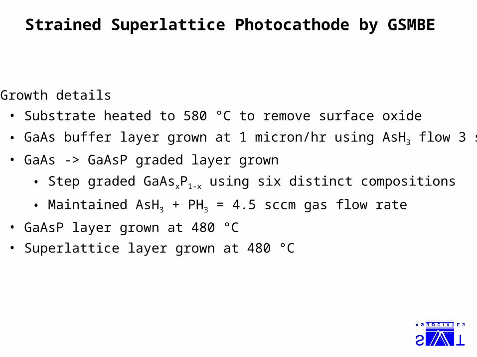
Strained Superlattice Photocathode by GSMBE
• Growth details
• Substrate heated to 580 °C to remove surface oxide
• GaAs buffer layer grown at 1 micron/hr using AsH3 flow 3 sccm
• GaAs -> GaAsP graded layer grown
• Step graded GaAsxP1-x using six distinct compositions
• Maintained AsH3 + PH3 = 4.5 sccm gas flow rate
• GaAsP layer grown at 480 °C
• Superlattice layer grown at 480 °C

Material Characterization- X-ray

Material Characterization- Photoluminescence

Material Characterization- Photoluminescence
Half die,PL points for uniformity probe

Conclusion
• Strained layers for photocathode applications
• Molecular beam epitaxy successful method for photocathode growth
• MBE growth parameters and structure can be refined to improve polarization of devices