上海坤道信息技术有限公司 - in this issue · please contact aavid or ats for more...
TRANSCRIPT

may 2011 | Volume V | Issue V
pediaATCA Standards For Thermo-Mechanical Considerations
Miniature Refrigerator For A Laptop
Thermal Simulation and Management of 3D Stacked Chip
JEDEC: Review Of Standards On Compact Thermal Modeling
Cooling News
IN THIS ISSUE

Advanced Thermal Solutions is a leading engineering and manufacturing company supplying com-plete thermal and mechanical packaging solutions from analysis and testing to final production. ATS provides a wide range of air and liquid cooling solutions, laboratory-quality thermal instrumentation, along with thermal design consulting services and training. Each article within Qpedia is meticulously researched and written by ATS’ engineering staff and contributing partners. For more information about Advanced Thermal Solutions, Inc., please visit www.qats.com or call 781-769-2800.
EDITOR KaVeH aZaR, Ph.D. President & CEO, Advanced Thermal Solutions, Inc.
MANAGING EDITORBaHmaN TaVassolI, Ph.D. Chief Technology Officer, Advanced Thermal Solutions, Inc.
NORTH AMERICA aDVaNCeD THeRmal soluTIoNs, INC. 89-27 Access Road Norwood, MA 02062 USA T: 781.769.2800 | F: 781.769.9979 | www.qats.com
EUROPE aDVaNCeD THeRmal soluTIoNs, B.V.De Nieuwe Vaart 50 | 1401 GS Bussum The Netherlands T: +31 (0) 3569 84715 | F: +31 (0) 3569 21294 www.qats-europe.com
All rights reserved. No part of this publication may be reproduced or
transmitted in any form or by any means, electronic, mechanical,
photocopying, recording or otherwise, or stored in a retrieval system
of any nature, without the prior written permission of the publishers
(except in accordance with the Copyright Designs and Patents Act 1988).
The opinions expressed in the articles, letters and other contributions
included in this publication are those of the authors; and the publication
of such articles, letters or contributions does not necessarily imply that
such opinions are those of the publisher. In addition, the publishers
cannot accept any responsibility for any legal or other consequences
which January arise directly or indirectly as a result of the use or adaptation
of any of the material or information in this publication.
ADVERTISING To PlaCe aN aD IN QPeDIa: Contact John O’ Day at 781.949.2521Qpedia was launched in 2007 as a technology eMagazine focused on the thermal management of electronics. It is designed as a resource to help the engineering community solve the most challenging thermal problems. The eMagazine is published monthly and distributed at no charge to over 17,000 engineers worldwide. Qpedia is also available online or for download at www.qats.com/qpedia.Qpedia’s editorial team includes ATS’ President & CEO, Kaveh Azar, Ph.D., and Bahman Tavassoli, Ph.D., the company’s chief technologist. Both Azar and Tavassoli are internationally recognized experts in the thermal management of electronics.
For more information on how you can generate awareness about your company or products, contact John o’ Day at 781.949.2521.
SUBSCRIBE ON LINE AT: www.qats.com/qpedia
2

2216106
may 2011 | Volume V | Issue V
Features
6 ATCA Standards For Thermo-Mechanical Considerations This is a basic overview of ATCA and provides a summary of some of the essential standards as well. It begins with a brief review of PICMG’s introduction of ATCA in 2002, and then goes on to discuss the key standards and/or requisite dimensions for boards, blades, shelf, subrack and chassis. In addition, there is a presentation of the typical guidelines for air temperature and pressure drops.
10 Miniature Refrigerator For A LaptopAs integrated circuits (ICs) have to provide increased functionality and computational power through a greater number of transistors in smaller and smaller packages, the removal of heat dissipated by these electronic chips has become a serious challenge in the design of portable and other space-limited electronic devices. This article explores some of the cooling options.
14 Thermal Simulation and Management of a 3D Stacked Chip As new generations of electronic devices are required for more functions, connectivity, versatility, and less weight, their sizes keep diminishing. These put enormous pressure on the chip design, device package and thermal management of such devices.
20 JEDEC: Review Of Standards On Compact Thermal ModelingThis article focuses on the thermal management of electronics and the JEDEC standard JC-15: “Thermal Characterization Techniques for Semiconductor Packages”. The scope of JC-15 includes the standard-ization of thermal characterization techniques, both testing (JED51) and modeling (JESD15) for electronic packages.
26 Cooling NewsNew products, services and events from around the industry.
3may 2011 |Qpedia

4
Two Thermal managemenT Powerhouses Join Forces
Aavid Thermalloy, LLC, the world’s oldest and one of the largest suppliers of thermal management products to the worldwide electronics marketplace, has signed a distribution agreement with Advanced Thermal Solutions, Inc. (ATS), a leader in innovative component cooling solutions. Aavid Thermalloy, with its global customer base and broad network of sales offices, representatives and distributors, will now have access to ATS’ high performance heat sink and attachment technologies to address the cooling of today’s and tomorrow’s electronic devices.
As part of the agreement, ATS will supply Aavid Thermalloy, with its complete line of maxiFLOW™ heat sinks whose patented design and thermal performance is unmatched in the electronics cooling market. In addition, Aavid Thermalloy will also distribute ATS’ patented maxiGRIP™ heat sink attachment systems. Its compact design securely attaches heat sinks to hot components on densely populated PCBs, and detaches quickly and cleanly when needed.
Please contact Aavid or ATS for more information regarding product availability.
aavid Thermalloy To globally disTribuTe aTs heaT sink and aTTachmenT ProducTs
“Around the world, the first name in heat sinks is Aavid Thermalloy. They’re the experts in thermal management technology and manufacturing and provide a worldwide distribution capability that marries uniquely to our innovative products...”
Dr. Kaveh Azar, President and CEOAdvanced Thermal Solutions, Inc.
“We’ve long recognized that ATS develops many of the industry’s most innovative heat
sinks and attachment systems, and that their products offer cooling solutions that can
benefit many of our worldwide customers...”Alan Wong, CEO
Aavid Thermalloy, LLC
Advanced Thermal Solutions, Inc. 89-27 Access Road | Norwood, MA | USAT: 781.769.2800 | F: 769.769.2800 www.qats.com
Aavid Thermalloy70 Commercial St. | Concord, NH | 03301 | USAT: 603.224.9988 | F: 603.223.1790www.aavidthermalloy.com

5 |Qpediaoctober 2009
ADVANCED THERMAL SOLUTIONS, INC. | 89-27 ACCESS ROAD, NORWOOD, MA 02062 USA | T: 781.769.2800 | QATS.COM
Contact the world’s foremost thermal management expertsReliability? Cost Reduction? Savings?
Click the QR symbol for our website
Need Direction?

66
ATCA Standards For Thermo-mechanical ConsiderationsIn 2002, the PCI Industrial Computer Manufacturers Group (PICMG) released a set of specifications known as Advanced Telecommunications Computing Architecture (ATCA). Also known as AdvancedTCA, these are open specifications that were designed for “carrier grade” communications equipment [1]. The specifications were designed to accommodate the latest technologies and incorporate them into a modular approach. The specifications were open so that different manufacturers could make products that are compatible to each other, decreasing costs and simplifying operation.
Since the main point of the ATCA standards is interoperability, the actual list of standards is very long and detailed. The base specification, which doesn’t even contain specifications for the Fabric (The method of data transmission), is a tome that would rival any college textbook. When working on projects that follow ATCA standards, the most important thing to remember is what types of things the standards dictate, and then it will be easy enough to look up the actual numbers.
ATCA is based around Front Board PCBs known as Blades. Blades plug into housings called Shelves, and can perform many different functions, such as routing data, providing server-based computing or housing mezzanine cards. In Figure 1 below, an example of a Blade is shown [2]. It would be correct to infer that Blades are often power-dense and must fit into a limited amount of space, judging by the use of expensive copper heat sinks and angled memory modules.
Physically, the Front Board must be 280 D X 322.25 H (mm), which is approximately 11” X 13” [3]. The board may weigh up to 4 kg, and must fit into a slot that is 30.48 mm wide. Component keepout zones of 4.5 mm along the top and bottom edges of the board allow the board to slide into alignment rails in the housings in which they will reside. The board offset is dictated, of course, and leaves an allowance of 21.33 mm for maximum component height, as illustrated below in Figure 2. This leaves a 2.54 mm no-component zone between boards.
Figure 2 also shows the required Component Side 2 cover, which must be metal to shield EMI and limit the spread of fire. After accounting for warpage of both the board and the cover, the component height on Side 2 is typically limited to less than 2 mm, and details are listed in the ATCA specification.Other important requirements for the front board are a metal face plate with standardized LEDs, two handles and an EMI gasket. In addition to fixed dimensions for those parts, the handles must have switches on them to facilitate hot-swapping of boards. As the controlled discharge of static is important during board insertion, there are detailed specifications regarding ESD strips along the bottom edge of the board.
Figure 1- Example of an ATCA Blade [2]
Figure 2- ATCA Front Board Component Height
7
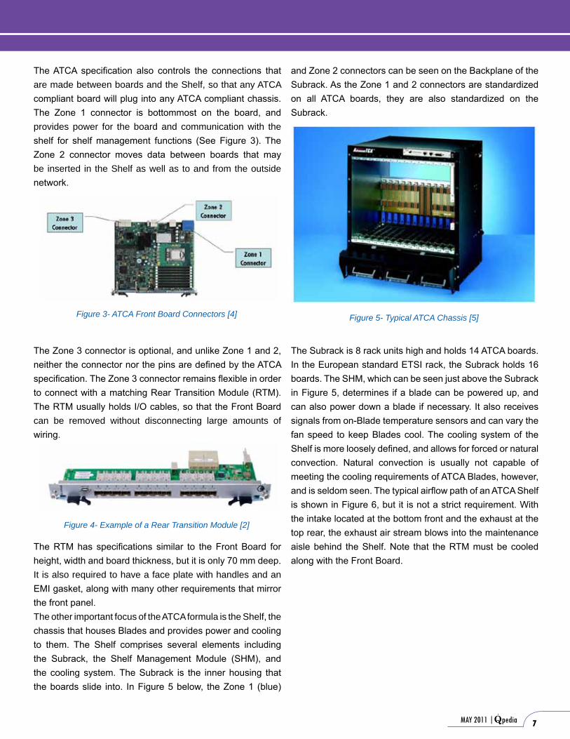
The ATCA specification also controls the connections that are made between boards and the Shelf, so that any ATCA compliant board will plug into any ATCA compliant chassis. The Zone 1 connector is bottommost on the board, and provides power for the board and communication with the shelf for shelf management functions (See Figure 3). The Zone 2 connector moves data between boards that may be inserted in the Shelf as well as to and from the outside network.
The Zone 3 connector is optional, and unlike Zone 1 and 2, neither the connector nor the pins are defined by the ATCA specification. The Zone 3 connector remains flexible in order to connect with a matching Rear Transition Module (RTM). The RTM usually holds I/O cables, so that the Front Board can be removed without disconnecting large amounts of wiring.
The RTM has specifications similar to the Front Board for height, width and board thickness, but it is only 70 mm deep. It is also required to have a face plate with handles and an EMI gasket, along with many other requirements that mirror the front panel.The other important focus of the ATCA formula is the Shelf, the chassis that houses Blades and provides power and cooling to them. The Shelf comprises several elements including the Subrack, the Shelf Management Module (SHM), and the cooling system. The Subrack is the inner housing that the boards slide into. In Figure 5 below, the Zone 1 (blue)
and Zone 2 connectors can be seen on the Backplane of the Subrack. As the Zone 1 and 2 connectors are standardized on all ATCA boards, they are also standardized on the Subrack.
The Subrack is 8 rack units high and holds 14 ATCA boards. In the European standard ETSI rack, the Subrack holds 16 boards. The SHM, which can be seen just above the Subrack in Figure 5, determines if a blade can be powered up, and can also power down a blade if necessary. It also receives signals from on-Blade temperature sensors and can vary the fan speed to keep Blades cool. The cooling system of the Shelf is more loosely defined, and allows for forced or natural convection. Natural convection is usually not capable of meeting the cooling requirements of ATCA Blades, however, and is seldom seen. The typical airflow path of an ATCA Shelf is shown in Figure 6, but it is not a strict requirement. With the intake located at the bottom front and the exhaust at the top rear, the exhaust air stream blows into the maintenance aisle behind the Shelf. Note that the RTM must be cooled along with the Front Board.
may 2011 |Qpedia
Figure 3- ATCA Front Board Connectors [4]
Figure 4- Example of a Rear Transition Module [2]
Figure 5- Typical ATCA Chassis [5]

8
Along with the recommendations are hard requirements, however, such as mandatory air filtering, which must trap over 80% of dust, and honeycomb or perforated metal screens for EMI control at the air intake and outlet. In addition, the Shelf should straighten airflow and provide roughly equal airflow to all of the Blades. In practice, however, it is commonly seen that Blades in the first and last slots receive reduced airflow.Typical guidelines allow for an air temperature increase of 10ºC when the ambient temperature (Ta) is 55ºC, which can be problematic when working with higher powered boards. There are hard limits on temperature of the face plate of a board, with 70ºC being the limit with a Ta of 55ºC. The ATCA specification allows boards which consume up to 400 W, but less than 200 W is preferred. As the telecom industry pushes more and more powerful boards, however, we are beginning to see Shelves that are designed to support Blades over 300 W. Not far in the future, Shelves that incorporate sub-ambient refrigeration cooling or other alternative cooling techniques will become more common. One example of this would be the Therm-Jett air jet-impingement cooling system mentioned in the April 2011 issue of Qpedia [6].The ATCA specification also defines the pressure drop across a board, with a maximum of 49.8 Pa (0.2” H2O) at 30 CFM. The preferred pressure drop is 37 Pa, and if the pressure drop is too low, baffles must be added to the board to restrict air flow. Likewise, if a board is removed from a Shelf, a dummy board with baffles must be inserted into the empty slot to prevent excess air bypass around active cards.
This introduction to ATCA standards should be seen as a starting point, and is not comprehensive by any means. The full standard is available from PICMG [1] and is indispensable to anyone working with ATCA compliant components. In addition to the mechanical aspects touched on here, specifics for platform management, electrical design and other topics are laid out.
References:1. “PICMG – Resources,” http://www.picmg.org/v2internal/resourcepage2.cfm?id=2, [May 4, 2011]. 2. ”Packet: PP50 Dual XLR,” http://www.ccpu.com/atca-advancedtca- products/packet-pp50-dual-netlogic-xlr/, [May 16, 2011]. 3. PICMG. “PICMG 3.0 R3.0 AdvancedTCA Base Specification,” March 24, 2008. 4 . “Promentum ATCA-4500,” http://www.radisys.com/Products/ATCA/Processing-Modules/Promentum- ATCA-4500.html, [March 31, 2011]. 5. ”System 12 U, 14 slot,” http://web.schroff.de/media/images/gross/12705005.jpg , [May 16, 2011]. 6. Azar, K., Tavassoli B., “Thermal Management Strategies For High Heat Flux Electronic Devices,” Qpedia, Volume V, Issue IV, April 2011.
Figure 6- Typical Airflow in an ATCA Shelf [5]
Innovation & DistributionUnlimited Capability
Click the QR symbol for aavid.com
Click the QR symbol for qats.com

9may 2011 |Qpedia
Advanced Thermal Solutions, Inc. (ATS) now offers the complete editorial contents of its widely-read Qpedia Thermal eMagazine in three hardbound volumes. The books provide an expert resource for design engineers,engineering managers, and others who want to learn more about the theories and applications of electronics thermal management. The three volume set contains nearly 150 in-depth articles, researched and written by veteran engineers. They address the most critical areas of electronics cooling, with a wide spectrum of topics and thorough technical explanation.
Books Available Individually, or in Book Sets at a Discount Price.
Volumes 1 - 3 Now Available in Hardcover Books
Click the QR symbol to order now
Miniature Refrigerator For a laptop
10
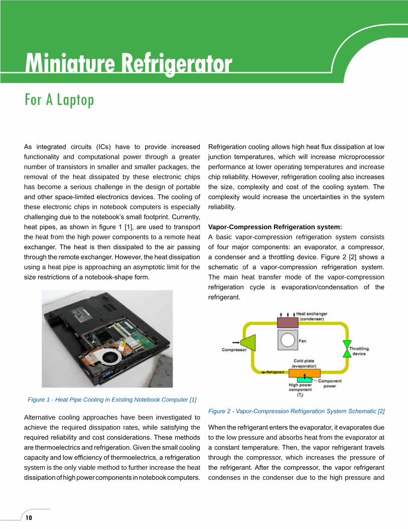
As integrated circuits (ICs) have to provide increased functionality and computational power through a greater number of transistors in smaller and smaller packages, the removal of the heat dissipated by these electronic chips has become a serious challenge in the design of portable and other space-limited electronics devices. The cooling of these electronic chips in notebook computers is especially challenging due to the notebook’s small footprint. Currently, heat pipes, as shown in figure 1 [1], are used to transport the heat from the high power components to a remote heat exchanger. The heat is then dissipated to the air passing through the remote exchanger. However, the heat dissipation using a heat pipe is approaching an asymptotic limit for the size restrictions of a notebook-shape form.
Alternative cooling approaches have been investigated to achieve the required dissipation rates, while satisfying the required reliability and cost considerations. These methods are thermoelectrics and refrigeration. Given the small cooling capacity and low efficiency of thermoelectrics, a refrigeration system is the only viable method to further increase the heat dissipation of high power components in notebook computers.
Refrigeration cooling allows high heat flux dissipation at low junction temperatures, which will increase microprocessor performance at lower operating temperatures and increase chip reliability. However, refrigeration cooling also increases the size, complexity and cost of the cooling system. The complexity would increase the uncertainties in the system reliability.
Vapor-Compression Refrigeration system:A basic vapor-compression refrigeration system consists of four major components: an evaporator, a compressor, a condenser and a throttling device. Figure 2 [2] shows a schematic of a vapor-compression refrigeration system. The main heat transfer mode of the vapor-compression refrigeration cycle is evaporation/condensation of the refrigerant.
When the refrigerant enters the evaporator, it evaporates due to the low pressure and absorbs heat from the evaporator at a constant temperature. Then, the vapor refrigerant travels through the compressor, which increases the pressure of the refrigerant. After the compressor, the vapor refrigerant condenses in the condenser due to the high pressure and
Figure 1 - Heat Pipe Cooling in Existing Notebook Computer [1]
Figure 2 - Vapor-Compression Refrigeration System Schematic [2]

11
rejects heat to the condenser at constant temperature. The refrigerant then travels through a throttling device, which reduces the liquid refrigerant pressure. The low pressure liquid refrigerant re-enters the evaporator and restarts the cycle. Figure 3 [2] shows the thermodynamic state point diagram of a vapor compression cycle.
For electronic cooling, the evaporator would be directly attached to the high power electronic chip, absorbing the chip’s heat dissipation. The heat dissipation would be rejected to the ambient environment through the air-cooled condenser. Figure 4 [3] shows the schematic of the vapor-compression cycle within a computer.
Figure 3 - Vapor Compression Cycle Thermodynamic State Point Diagram [2]
Recently, there have been a lot of studies that aim to further investigate the feasibility of the refrigeration system for electronics cooling. Studies of vapor compression systems and system simulation were directed at electronics cooling in laptop computers. One such study was conducted by Mongia, Masahiro, and DiStefano. The small-scale refrigeration system, within the study, included a compressor, cold plate, condenser and throttling device. These components were specially designed, such that the entire cooling system can be incorporated within a notebook form factor. Figure 5 [2] shows the schematic of the entire system with temperature and pressure measurement points.
may 2011 |Qpedia
Figure 4 - Schematic of a Miniature Refrigeration System [3]
Figure 5 - Small Scale Refrigeration System Schematic [2]
12
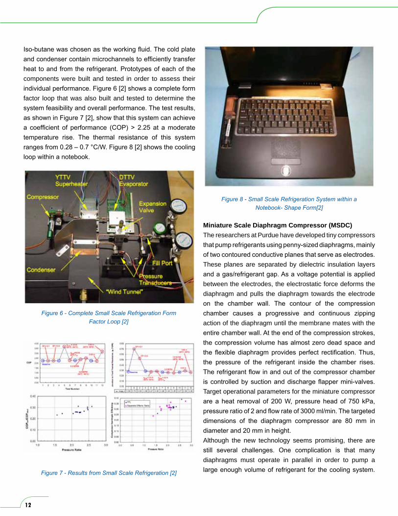
Iso-butane was chosen as the working fluid. The cold plate and condenser contain microchannels to efficiently transfer heat to and from the refrigerant. Prototypes of each of the components were built and tested in order to assess their individual performance. Figure 6 [2] shows a complete form factor loop that was also built and tested to determine the system feasibility and overall performance. The test results, as shown in Figure 7 [2], show that this system can achieve a coefficient of performance (COP) > 2.25 at a moderate temperature rise. The thermal resistance of this system ranges from 0.28 – 0.7 °C/W. Figure 8 [2] shows the cooling loop within a notebook.
Miniature Scale Diaphragm Compressor (MSDC)The researchers at Purdue have developed tiny compressors that pump refrigerants using penny-sized diaphragms, mainly of two contoured conductive planes that serve as electrodes. These planes are separated by dielectric insulation layers and a gas/refrigerant gap. As a voltage potential is applied between the electrodes, the electrostatic force deforms the diaphragm and pulls the diaphragm towards the electrode on the chamber wall. The contour of the compression chamber causes a progressive and continuous zipping action of the diaphragm until the membrane mates with the entire chamber wall. At the end of the compression strokes, the compression volume has almost zero dead space and the flexible diaphragm provides perfect rectification. Thus, the pressure of the refrigerant inside the chamber rises. The refrigerant flow in and out of the compressor chamber is controlled by suction and discharge flapper mini-valves. Target operational parameters for the miniature compressor are a heat removal of 200 W, pressure head of 750 kPa, pressure ratio of 2 and flow rate of 3000 ml/min. The targeted dimensions of the diaphragm compressor are 80 mm in diameter and 20 mm in height.Although the new technology seems promising, there are still several challenges. One complication is that many diaphragms must operate in parallel in order to pump a large enough volume of refrigerant for the cooling system.
Figure 6 - Complete Small Scale Refrigeration Form Factor Loop [2]
Figure 7 - Results from Small Scale Refrigeration [2]
Figure 8 - Small Scale Refrigeration System within a Notebook- Shape Form[2]

13
One possible solution is to stack the diaphragms within the system small enough to fit inside a laptop. The design can be optimized using computational methods, which enables the engineers to determine how many diaphragms to use and how to stack them, either in parallel to each other or in series. By stacking in one direction, the pressure might increase. While stacking in the other direction, the necessary volume would be able to be pumped. Another major challenge is to manufacture the compressors at a low cost.
Micro-channel heat sinks:Another research project at Purdue is focusing on heat transfer in microchannel heat sinks, which circulate coolant through numerous channels about three times the width of a human hair. The micro-channel heat sink is a copper plate containing numerous grooves 231 microns wide – or about three times as wide as a human hair – and 713 microns deep. Figure 10 [5] shows Purdue researchers testing their microchannel heat sinks.
Figure 9 - Miniature Diaphragm Compressor Schematic [4]
Figure 10 - Purdue Researchers Testing Micro-Channel Heat Sink [5]
Currently the researchers at Purdue are seeking to characterize and predict the enhancement due to boiling heat transfer provided by randomly roughen the surfaces in micro-channel heat sinks. Some results indicate that increasing the surface roughness by a factor of 3 yields a 30% enhancement in the amount of heat that can be removed while keeping the heat sink temperature constant. Further increases in surface roughness appear to be of little additional benefit.There has been a lot of research in the feasibility and operational performance of small scale vapor-compression system. One promising area is the microchannel heat exchanger, which circulates coolant through numerous channels about three times the width of a human hair. Another promising area is a micro-diaphragm compressor. As the challenge of heat removal from more powerful electronic chips in smaller form shape increases, small scale vapor-compression system might be a promising solution.
References:1. “Review Core Duo vs. Core 2 Duo”, NotebookCheck website http://www.notebookcheck.net/Review-Core-Duo-vs-Core-2- Duo.2404.0.html2. Mongia R. et al., “Small Scale Refrigeration System for Electronics Cooling within a Notebook Computer”, Proceedings SEMITHERM XXII, March 2006, San Clara, pp.751-7583. “Miniature Refrigeration System for Electronics Cooling”, Minicool website http://www.minicool.co.uk/project.html4. “CTRC Breakthroughs”, CTRC website https://engineering.purdue.edu/CTRC/research/breakthroughs.php5. “Purdue Miniature Cooling Device Will Have Military, Computer Uses”, ScienceDaily website http://www.sciencedaily.com/releases/2005/04/050414173948.htm6. “Miniature Cooling Device”, California Science & Technology News website http://www.ccnmag.com/article/miniature_cooling_device7. Trutassanawin S. et al., “Experimental Investigation of a Miniature-Scale Refrigeration System for Electronics Cooling”, CTRC Research Publications, Sept. 2006, pp.678-687.8. Chiriac V., Chiriac F., “Optimized Refrigeration Vapor Compression System for Power Microelectronics Cooling”, Proceedings of Clima 2007 WellBeing Indoors.
may 2011 |Qpedia

14
Thermal Simulationand management of a 3D stacked Chip
As new generations of electronic devices are required for more functions, connectivity, versatility, and less weight, their sizes keep on diminishing. These put enormous pressure on the chip design, device package and the thermal management of such devices. To put more functions into smaller size devices requires electrical and mechanical engineers to find intuitive ways to create new products.System on Chip (SOC) refers to integrating all components of an electronic system into a single integrated chip. It may contain digital, analog, mixed-signal and, often, radio- frequency functions – all on a single chip substrate. A typical application is in the area of embedded systems, such as microcontrollers or smart phone chips. Stacked multi-chip design is an effective way to construct such a system on a chip module. Figure 1 shows a photo of a 3D stacked multichip module. This multichip module has four dies stacked on top of each other. The first die sits on the substrate and it is the largest in size. The second die sits on top of first die and they are separated by a silicon spacer. Its size is smaller than the first die. The third die sits on top of second die and bonds together with it. The forth die is smallest and is set on top of the third die. The electrical wires of all dies come down to the interconnectors on the substrate. In most cases, the interconnectors are extended outside through the conventional ball grid array (BGA) on the other side of substrate.
The advantages of using multi-chip module packaging includes: 1. Increased package density and performance, reduced chip size and weight 2. Added value on high-speed designs, improved signal integrity and assembly 3. Improved interconnection performance 4. Reduced chip restate area and overall power5. Reduced board area and routing complexity at the next level.
The challenges of using multi-chip module packaging include:1. Package parasites often affect signal matching, noise coupling and attenuation2. Requires comprehensive 3D electromagnetic and mechanical analysis3. Chip size, placement and thickness of interposer can affect the thermal stresses4. Differences in the coefficients of thermal expansion coefficients result in differential thermal strain that induces stresses5. Possible delamination and voids provide large thermal resistance and cause thermal problems in vertical stacked die package6. Thermal management of multi-chip structure is difficult
For the mechanical and thermal engineer, challenges 3-6 are major concerns. From the point of view of thermal management, the prediction of the thermal resistance from dies to ambient and the temperature distribution in multiple dies is the main focus. Reducing the die junction temperature is, however, the ultimate goal.
Figure 1- 3D Stacked Multichip Module [1]

15may 2011 |Qpedia
Cumulative structure function gives the sum of the thermal capacitances (cumulative thermal capacitance) as a function of the sum of the thermal resistances (cumulative thermal resistance) of a system, measured from the point of excitation towards the ambient [2]. Figure 1 shows one example of the cumulative structure function.
The differential structure function is defined as the derivative of the cumulative thermal capacitance with respect to the cumulative thermal resistance,
For a wide slice of single matter with cross section area A,
and,
where c is the volumetric heat capacitance and k is the thermal conductivity.The K value of the differential structure function is,
The value K is proportional to the volumetric heat capacitance c, thermal conductivity k, and to the square of the cross sectional area A. As it is stated by Rencz and Székely in their paper [2], this function provides a map of the square of the heat current-flow cross section area as a function of the cumulative resistance. In these functions the local peaks indicate reaching new surfaces (materials) in the heat flow path, and their distance on the horizontal axis gives the partial thermal resistances between these surfaces. More precisely the peaks point usually to the middle of any new region where both the areas, perpendicular to the heat flow and the material are uniform.Rencz and Székely investigated a chip with three stacked dies by numerical simulation [2]. One quarter of the investigated pyramidal structure is illustrated in Figure 3. The size of the bottom die was 14x14 mm (7x7 in the ¼ simulation), the die size in the middle was 12x12 mm, and the size of the top die was 10x10 mm. The thickness of all the die and the glue layers were 0.035 mm. The considered thermal conductivity and volumetric thermal capacity values were 156 W/m.K and 1.6×10⁶ W.s/m2K for the silicon, 1 W/mK and 1×10⁶ W.s/m2K for the glue layers. The heat dissipating area is located in the middle of the top layer and the considered heat transfer coefficients were 6000 W/m2.K on the bottom and 100 W/m2.K on the top. The main heat flux is transferred to outside through the bottom of the package.
Figure 3. The Investigated Pyramidal Structure [2]
Figure 2. The Cumulative Structure Function and the Related Cauer Equivalent Circuit [2]
(1)
(2)
(3)
(4)

16
The simulation results of Rencz and Székely’s study [2] are shown in Figure 4 and 5. Figure 4 shows the cumulative structure function and Figure 5 shows the differential structure function of the Pyramidal structure. The thermal resistance and thermal capacitance values of each die can be read and calculated directly from the above figures.To model the 3D stacked die structure analytically, compact RC model can be used. Figure 6 shows one example for a chip with 2 stacked dies. By using such model and die resistance obtained for structure function curve, engineers can easily predict the die temperature at different electrical loads.
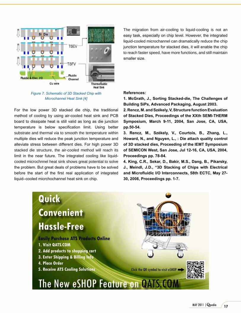
The thermal simulation and modeling of 3D stacked chip are essential to understand the parameters and material properties that affect the thermal resistance and die temperature. But to solve the ever-growing problem of increasing heat flux load, innovative methods have to be used to remove heat of the dies and alleviate the die temperature.The current and future cooling technologies for stacked die structure include:1. Thermal vias and inter-plain heat spreaders2. Single phase microchannel liquid cooling3. Two-phase microchannel liquid coolingThe thermal vias provides the dies with thermal paths to heat sink or cold plate. The inter-plain heat spreaders smooth the temperature in the die and reduce the hot spots. They also help to transfer the heat to the case. The single-phase/two-phase liquid-cooled microchannel can be directly etched on silicon wafer by using same technology to make chips. So the microchannel can be integrated in 3D stacked die structure. Due to its miniature channel size, microchannel heat sinks can achieve extreme high convection heat transfer coefficient and low thermal resistance. Figure 6 shows a 3D stacked die with integrated liquid-cooled microchannel heat sink.
Figure 4. The Cumulative Structure Function of the Pyramidal Structure
Figure 6. Compact Thermal Model of Package with 2 Stacked Dies [3]
Figure 5. The Structure Function of the Pyramidal Structure [4]
17may 2011 |Qpedia
For the low power 3D stacked die chip, the traditional method of cooling by using air-cooled heat sink and PCB board to dissipate heat is still valid as long as die junction temperature is below specification limit. Using better substrate and thermal via to smooth the temperature within multiple dies will reduce the peak junction temperature and alleviate stress between different dies. For high power 3D stacked die structure, the air-cooled method will reach its limit in the near future. The integrated cooling like liquid-cooled microchnnel heat sink shows great potential to solve the problem. But great deals of problems have to be solved before the start of the first real application of integrated liquid–cooled micrchochannel heat sink on chip.
The migration from air-cooling to liquid-cooling is not an easy task, especially on chip level. However, the integrated liquid-cooled microchannel can dramatically reduce the chip junction temperature for stacked dies, it will enable the chip to reach faster speed, have more functions, and still maintain smaller size.
References:1. McGrath, J., Sorting Stacked-die, The Challenges of Building SiPs, Advanced Packaging, August 2003.2. Rencz, M. and Székely, V, Structure function Evaluation of Stacked Dies, Proceedings of the XXth SEMI-THERM Symposium, March 9-11, 2004, San Jose, CA, USA, pp.50-54.3. Rencz, M., Székely, V., Courtois, B., Zhang, L., Howard, N., and Nguyen, L., : Die attach quality control of 3D stacked dies, Proceeding of the IEMT Symposium of SEMICON West, San Jose, Jul 12-16, CA, USA, 2004, Proceedings pp. 78-84.4. King, C.R., Sekar, D., Bakir, M.S., Dang, B., Pikarsky, J., Meindl, J.D., “3D Stacking of Chips with Electrical and Microfluidic I/O Interconnects, 58th ECTC, May 27-30, 2008, Proceedings pp. 1-7.
Figure 7. Schematic of 3D Stacked Chip with Microchannel Heat Sink [4]
QuickConvenientHassle-Free
The New eSHOP Feature on QATS.COM
Easily Purchase ATS Products Online1. Visit QATS.COM2. Add products to shopping cart3. Enter Shipping & Billing Info4. Place Order5. Receive ATS Cooling Solutions Click the QR symbol to visit eSHOP
18
Digi-Key is an authorized distributor for all supplier partners. New products added daily. © 2011 Digi-Key Corporation, 701 Brooks Ave. South, Thief River Falls, MN 56701, USA
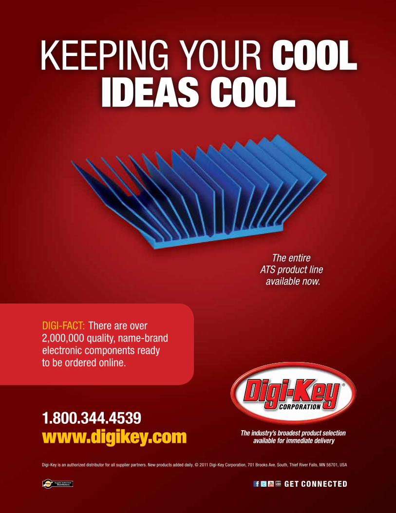
DIGI-FACT: There are over 2,000,000 quality, name-brand electronic components ready to be ordered online.
The entire ATS product line
available now.
KEEPING YOUR COOL IDEAS COOL
1.800.344.4539www.digikey.com

19may 2011 |QpediaADVANCED THERMAL SOLUTIONS, INC. | 89-27 ACCESS ROAD, NORWOOD, MA 02062 USA | T: 781.769.2800 F: 781.769.9979 | WWW.QATS.COM
Work with trusted advisors with 150 years of collective thermal management experience and innovative thinking. Benefit from their advanced testing facilities and best practices.
From consulting to custom designs, ATS takes the risk out of decision-making. Call us today at 781.769.2800, email [email protected] or click the QR symbol for our website
REMOVE UNCERTAINTY. GO TO MARKET FIRST. AVOID RECALLS.
SHORTCUTS CAN BE RISKY!

At the time when a gallon of gas was $.25 and the integrated circuit was deemed “invented”, an organization was formed known as JEDEC. The Joint Electron Devices Engineering Council is now made up of more than 3,000 volunteers from nearly 300 companies around the globe. The 50+ committees have a common vision: to create an evolving set of standards to ensure product interoperability, reduce cost and time to market. As a result, companies can base their designs on a set of standards and focus more on R&D. The resulting benefit is less time invested on product invention and more on innovation.
To maintain consistency with Qpedia, this article will focus on the thermal management of electronics and the JEDEC standard JC-15: Thermal Characterization Techniques for Semiconductor Packages. The scope of JC-15 includes thestandardization of thermal characterization techniques, both testing (JESD51) and modeling (JESD15), for electronic packages, components and materials for semiconductor devices. For a closer look at standard JESD51 and the Thermal Measurement Methods of an Integrated Circuit, please look through the Qpedia archives and review an article in the June, 2007 issue titled: “Understanding the JEDEC Integrated Circuit Thermal Test Standards”.
The electronic industry has evolved such that new components are outperforming their predecessors. Packages are outputting more power, yet getting smaller in size, and operating at increasing temperatures. As we know in Thermal Engineering and as a Provider of Heat Sinks at Advanced Thermal Solutions, insuring that components are operating within the specified range is usually the last thing
thought of when bringing new products through the design phase. These are highly 3D problems; insomuch as, in addition to the power of the devices, there can be increases in temperature due to the environment such as airflow characteristics, thermal coupling of neighboring devices, system altitude, etc. All possibilities must be taken into account when looking at how the entire system will operate.
When looking at a system, the greatest points of concern are the Junction Temperatures (Tj). As defined by JEDEC: “Absolute maximum rated junction temperature is the maximum junction temperature of an operating device, beyond which damage (latent or otherwise) may occur; it is frequently specified by device manufacturers for a specific device and/or technology” [1]. Figure 1 shows the junction location and an example of how a semiconductor can be packaged and installed onto a PCB.
During operation, The Tj must be monitored and maintained within the range specified by the device manufacturer. This is because temperatures outside the range speed up chemical reactions and accelerate changes in materials. This produces distortion stress on the junction between
20
JEDEC: Review Of Standards on Compact Thermal modeling
Figure 1 – Package Attached to PCB via BGA
21
two materials with different expansion rates. If this occurs repeatedly, material fatigue arises, causing failures such as hermetic seal damage, die bond adhesion damage and bonding wire opens. In addition, if the device is used with improper connections, the heat generated from the equipment or element can accelerate the temperature change and affect the product in an accelerated manner. [3]
The ranges differ per application; for example, the temperature range of a Xilinx Spartan -6 FPGA is:C = Commercial (Tj = 0ºC to +85ºC)I = Industrial (Tj = -40ºC to +100ºC)
Xilinx denotes this range in the item number by ending with a “C,” or an “I.” Check your own device manufacturer for the operating range for your application i.e., Commercial, Industrial, or Military.
For users to maintain a safe Tj, we must know the semiconductor’s thermal resistance. Due to the fact that semiconductors need to perform in a wide array of environmental (surroundings, mounting, etc.), electrical (power levels, currents, voltages, etc.) suppliers must adhere to a standardized approach to defining the thermal resistance. It is by these means that both the manufacturer and the user can determine an accurate Tj.Thermal modeling is constantly becoming more significant in the characterization of components and for predicting Tj for standard testing, as well as within the applications environment. The resulting data can be used by design engineers in evaluating the package itself, its reliability and to analyze the thermal performance of the entire system.Due to the complexity of system level analysis, engineers would sometimes be constructing simulations with a lack of information. This resulted in an increased time investment to create an accurate model. Because of this, JEDEC decided that it made more sense for the suppliers themselves to characterize their own products for end users. There are several benefits to this approach. One major benefit is that the suppliers protect themselves by ensuring the accuracy of the thermal performance of their products and models released to their customers. In addition, if the models were said to be performed by the user, the supplier would lose
any control over the accuracy of the data resulting from simulation.
JEDEC has introduced to the standards, Compact Thermal Models (CTM), to insure accuracy and compatibility throughout the industry, while providing a way for suppliers to share data effectively with global customers. A CTM is a way to “hone— in” on the component package and achieve a high level of boundary condition impedance (BCI), so that the thermal behavior of that component can be supplied for system level simulation. There are two methods defined by JEDEC, they are: The Two Resistor Model, and The DELPHI Model. These models are described below and are illustrated in Figures 2 and 4; but, first, let’s look at the properties and assumptions that were made when creating these models:
Properties: • Limited Complexity (10’s of Nodes) • Vendor/Software Neutral • Adaptable to mainstream conduction codes for package-level thermal analysis • Capable of insertion into standard numerical codes for system/board-level analysis • Absolute BCI property is when CTM calculates chip temperature in all possible environments in agreement with results of detailed model calculation • Fully documented, nonproprietary
Assumptions: • Package contains single IC with each node representing a single temperature region • Package mounted to a PCB • Heat flows from the chip package to the:– Top surface to ambient fluid or heat sink – Side surfaces to ambient fluid – Bottom surface / leads to PCB• Thermal resistor networks are used to represent heat flow paths • External surfaces can either be:– Considered isothermal and represented by single nodes – Subdivided into isothermal regions with corresponding nodes
may 2011 |Qpedia
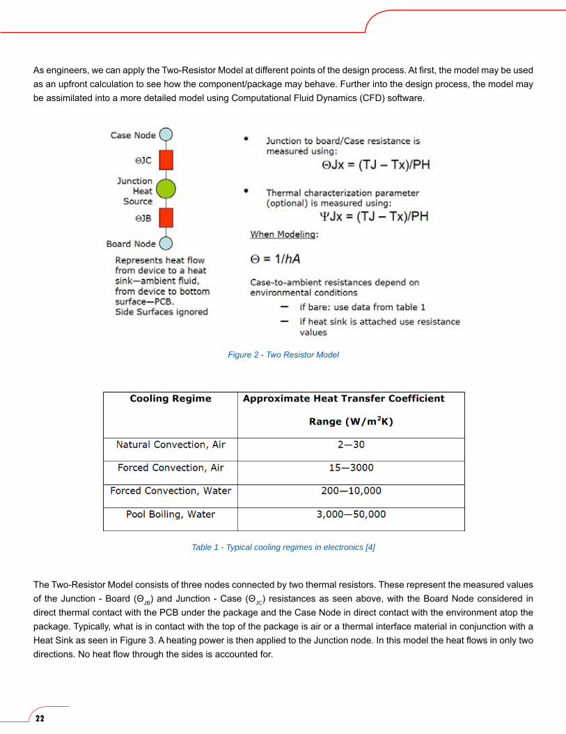
As engineers, we can apply the Two-Resistor Model at different points of the design process. At first, the model may be used as an upfront calculation to see how the component/package may behave. Further into the design process, the model may be assimilated into a more detailed model using Computational Fluid Dynamics (CFD) software.
The Two-Resistor Model consists of three nodes connected by two thermal resistors. These represent the measured values of the Junction - Board (ΘJB) and Junction - Case (ΘJC) resistances as seen above, with the Board Node considered in direct thermal contact with the PCB under the package and the Case Node in direct contact with the environment atop the package. Typically, what is in contact with the top of the package is air or a thermal interface material in conjunction with a Heat Sink as seen in Figure 3. A heating power is then applied to the Junction node. In this model the heat flows in only two directions. No heat flow through the sides is accounted for.
22
Figure 2 - Two Resistor Model
Table 1 - Typical cooling regimes in electronics [4]

23 |Qpediamay 2011
As noted, care should be taken because the model doesn’t consider environmental conditions, and these must be specified by the engineer at the Case and Board nodes. Furthermore, the error bounds cannot be determined from the generation of the model. They may be derived from comparing the engineer’s predictions with data from actual tests.
As technology has evolved, the use of 3D simulation tools has become nearly standard. Using programs such as CFDesignTM, and 6sigmaETTM can solve both the solid and air portions of the system directly. This is done by solving the Navier- Stokes equations which govern fluid flow and heat transfer. There is error in this method as well, as the program has to converge to a number. When setting up the CFD tool, care should be taken to ensure the correct interaction it will have with the surrounding flow. This is done by maintaining the physical geometry of the package. [4]Table 2 shows the process flow for a thermal network and a 3D simulation approach to the Two-Resistor Model.
Table 2 - Thermal Network and 3D Simulation Methods
Figure 3 - maxiFLOW/superGRIPTM Heat Sink with Thermal Interface Material

24
Even though less accurate, the intuitiveness and simplicity of the Two- Resistor model makes it attractive for engineers to construct. For a more complex and accurate approach, we shall look to the DELPHI project.
Much can be claimed by The DELPHI project. It is in fact, DELPHI (DEvelopment of Libraries of PHysical models for an Integrated design environment) that coined the term “Compact Thermal Model” (CTM) and started the movement to establish standard methods of usage and sharing of component characterizations. After 1996, subsequent projects such as SEED (Supplier Evaluation and Exploitation of DELPHI) and PROFIT (PRediction OF Temperature Gradients Influencing the Quality of Electronic Products) further develop publically the CTM, while members of each organization maintain their activity within JEDEC.
A DELPHI compact model is a thermal resistance network. This CTM is comprised of a limited number of nodes connected to each other by thermal resistor links (see Figure 4). With knowledge that the thermal problems are highly 3D, the heat flow within a component/package is represented in the model by a series of links. Network nodes are, by definition, each associated with a single temperature only. The nodes can be either surface or internal.
Surface nodes are associated with a physical region of the package surface defining the area of the node. In such a case, the nodal temperature represents the average temperature of the area allocated to the node in the actual package. Also, surface nodes must always have a direct one-to-one association with the corresponding physical areas on the actual package. Therefore, it is critical that they communicate with the environment in the same manner as the package. [5]
Figure 4 - DELPHI Model

25may 2011 |Qpedia
The objection function is the difference between the detailed model and the compact model summed over the boundary condition set and a finite number of points within the component package. [5]Minimizing the Objection function should result in a compact model that has a low error. Table 3 illustrates the generation flow for DELPHI model generation.
It is important to keep in mind that the availability of the DELPHI compact model does not eliminate the need for understanding the application in which the package is to be used. In other words, it is the user’s responsibility to take into account the environment surrounding the package. The environmental conditions for the relevant application must be applied at the surface nodes as boundary conditions. [5]There are a number of criteria that have been established to provide a comparison of the CTM methods. Table 4 shows the Criteria and the Application of it for each Model.
The objective of the Compact Thermal Models, as described, is to simplify a component or package, verify its thermal performance and install the findings into a system, and perform simulations to determine thermal behavior within relevant applications. It has been in the best interest of suppliers to construct these CTMs and validate their products so that users shall have confidence in the capabilities of those products. The electronics cooling industry is much like fashion, in that: what may be successful today, will be unworkable or impractical tomorrow. JEDEC and its application of the CTMs are constantly evolving with the innovation of simulation tools, components and their applications. Within an ever changing marketplace, JEDEC standards advocate increases in reliability, interoperability, cost reduction and decreases in time-to-market for products within the microelectronics industry.
References:1) JEDEC Standard, JESD22-A108D, June 2005, “Temperature, Bias, and Operating Life.”<http://www.jedec.org/standards-documents/docs/jesd-22-a108c> 2) Xilinx, March 21, 2011, “Spartan-6 Family Overview”<http://www.xilinx.com/support/documentation/data_sheets/ds160.pdf> 3) Toshiba Corporation, July 2010, “Operating Environment Factors.”<http://www.semicon.toshiba.co.jp/eng/product/reliability/device/concept/1186220_7655.html> 4) JEDEC Standard, JESD15-3, July 2008, “Two-Resistor Compact Thermal Model Guideline.”<http://www.jedec.org/sites/default/files/docs/JESD15-3.pdf> 5) JEDEC Standard, JESD15-4, October, 2008, “DELPHI Compact Thermal Model Guideline.” < http://www.jedec.org/sites/default/files/docs/JESD15-4.pdf>
Table 3 - Steps in Generating the DELPHI Compact Model.
Table 4 - CTM Criteria – Comparison
26
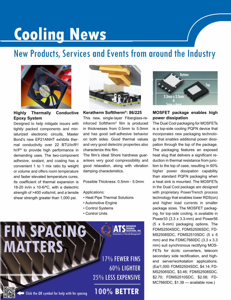
Highly Thermally Conductive Epoxy System Designed to help mitigate issues with tightly packed components and min-iaturized electronic circuits, Master Bond’s new EP21ANHT exhibits ther-mal conductivity over 22 BTU/in/ft2/hr/Fº to provide high performance in demanding uses. The two-component adhesive, sealant, and coating has a convenient 1 to 1 mix ratio by weight or volume and offers room temperature and faster elevated temperature cures. Its coefficient of thermal expansion is 18-20 in/in x 10-6/ºC, with a dielectric strength of >400 volts/mil, and a tensile shear strength greater than 1,000 psi.
Keratherm Softtherm®: 86/225This new, single-layer Fiberglass-re-inforced Softtherm® film is produced in thicknesses from 0.5mm to 5.0mm and has good self-adhesive behavior on both sides. Good thermal values and very good dielectric properties also characterize this film.The film’s ideal Shore hardness guar-antees very good compressibility and good relaxation, along with vibration damping characteristics.
Possible Thickness: 0.5mm - 5.0mm
Applications:• Heat Pipe Thermal Solutions• Automotive Engine• Control Systems• Control Units
MOSFET package enables high power dissipationThe Dual Cool packaging for MOSFETs is a top-side cooling PQFN device that incorporates new packaging technolo-gy that enables additional power dissi-pation through the top of the package. The packaging features an exposed heat slug that delivers a significant re-duction in thermal resistance from junc-tion to the top of case, resulting in 60% higher power dissipation capability than standard PQFN packaging when a heat sink is mounted. The MOSFETs in the Dual Cool package are designed with proprietary PowerTrench process technology that enables lower RDS(on) and higher load currents in smaller package sizes. The MOSFET packag-ing, for top-side cooling, is available in Power33 (3.3 x 3.3-mm) and Power56 (5 x 6-mm) packaging options. The FDMS2504SDC, FDMS2506SDC, FD-MS2508SDC, FDMS2510SDC (5 x 6 mm) and the FDMC7660DC (3.3 x 3.3 mm) suit synchronous rectifying MOS-FETs for dc/dc converters, telecom secondary side rectification, and high-end server/workstation applications. (Ea/1,000: FDMS2504SDC, $4.14; FD-MS2506SDC, $3.46; FDMS2508SDC, $2.70; FDMS2510SDC, $2.08; FD-MC7660DC, $1.38 — available now.)
Cooling News New Products, services and events from around the Industry
Click the QR symbol for help with fin spacing
FIN SPACING MATTERS
100% BETTER
17% FEWER FINS60% LIGHTER
25% LESS EXPENSIVE
2727
Highly Thermally Conductive Ep-oxy System Simulator features thermal, radiative cooling sur-faceThe CS-100 Thermal Chassis Simulator provides a thermal mass and radiative cooling surface for passive cooling of ADL CPUs. The 100-in.2 chassis is used with its universal mounting pattern and is compatible with all of the company’s PC/104 heat spreaders and pipes, regardless of the CPU. The product contains both M3 and 4-40 hardware, as well as standoffs to support 0.600- or 1.000-in. clearance spreaders. The thermal simulator is made from Blanchard-ground powder-cast plate aluminum. It has a surface flatness better than 0.001 in. across the entire face. The anodizing provides basic emissivity of ≤0.75 and represents the radiative area of an aluminum enclosure with 200-in.2 It is used as a development platform for proof-of-concept passive cooling systems. ($299 — available now.)
Fan provides 21-cfm air flowThe AG4015 fan measures 40 x 40 x 15 mm and features an impeller design that enables it to rotate at 15,000 rpm, and produce 21-cfm air flow. It provides static pressure of 0.92 in. of water while maintaining a 51-dBA noise levels. The fan is available with operating voltages of 5, 12, and 24 Vdc. It suits storage, networking, set-top box, game console, and power applications. Standard op-erating temperature ranges from 10 to +70C. Options include extended tem-perature ratings, IP-55 rated water pro-tection, on-board PWM control, alarm output, tachometer output, and therm-istor control. (Contact 561-241-6700 price and availability.)
JaNuaRy 2011 |Qpedia
Learn how to improve the capability & reliability of your heat sink
89-27 Access Road, Norwood, MA 02620 USA | T: 781.769.2800 | F: 781.769.9979 | www.qats.com 89-27 Access Road, Norwood, MA 02620 USA | T: 781.769.2800 | F: 781.769.9979 | www.qats.com
Low profile, spread fin array maximizes surface area for more effective convection cooling
Requires minimal “keep-out area”; ideal for densely populated PCB’s Provides tight, secure sink attachment in shock and vibration environments
Preassembled with hardware and high performance, phase changing TIM
Learn how to improve the capability & reliability of your heat sink
superGRIPTM
Click play to watch superGRIPTM in action
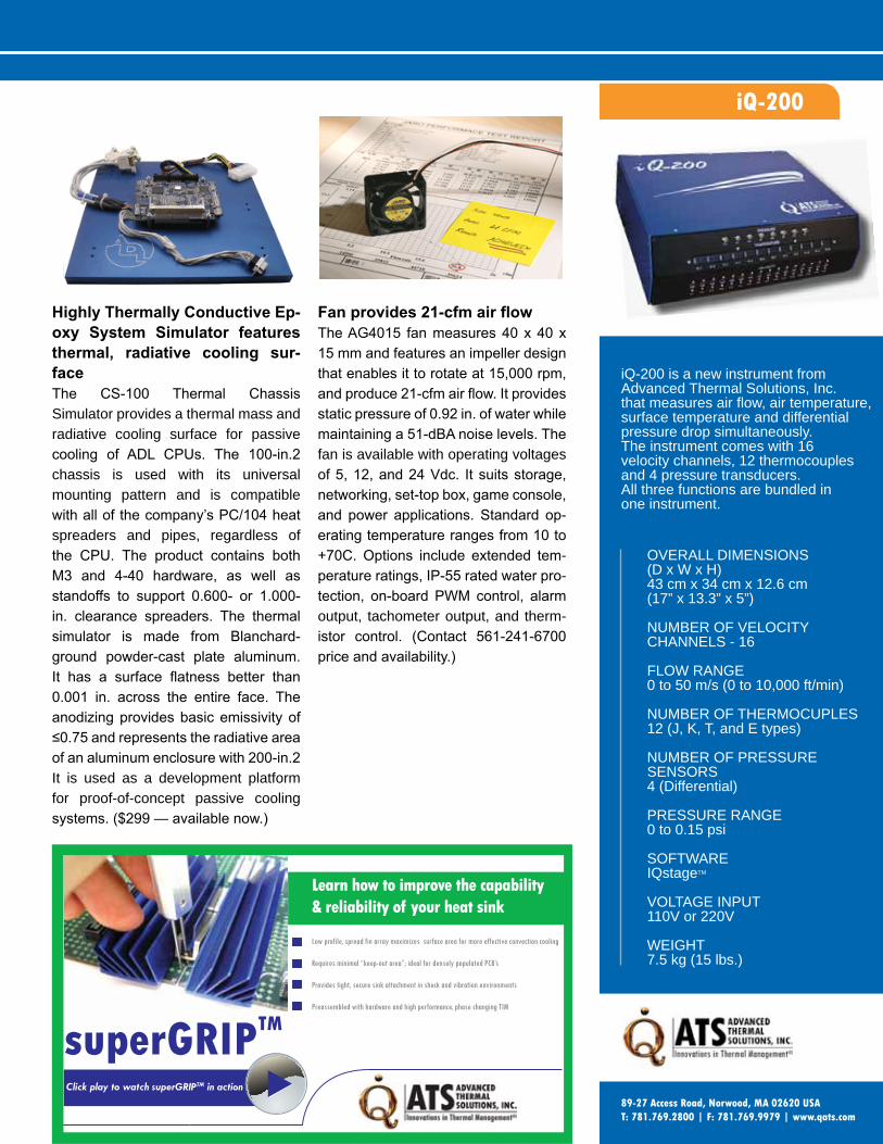
iQ-200
89-27 Access Road, Norwood, MA 02620 USA T: 781.769.2800 | F: 781.769.9979 | www.qats.com
OVERALL DIMENSIONS (D x W x H)43 cm x 34 cm x 12.6 cm(17” x 13.3” x 5”)
NUMBER OF VELOCITY CHANNELS - 16
FLOW RANGE0 to 50 m/s (0 to 10,000 ft/min)
NUMBER OF THERMOCUPLES12 (J, K, T, and E types)
NUMBER OF PRESSURE SENSORS4 (Differential)
PRESSURE RANGE0 to 0.15 psi
SOFTWAREIQstageTM
VOLTAGE INPUT110V or 220V
WEIGHT7.5 kg (15 lbs.)
iQ-200 is a new instrument from Advanced Thermal Solutions, Inc.that measures air flow, air temperature,surface temperature and differential pressure drop simultaneously.The instrument comes with 16 velocity channels, 12 thermocouplesand 4 pressure transducers. All three functions are bundled in one instrument.

28 28 |Qpediaoctober 2009
Getting your company’s message out to over 17,000 engineers and industry professionals has never been easier.
Advertise in Qpedia Today!Qpedia was launched in 2007 as a technology eMagazine focused on the thermal management of electronics. It is designed as a resource to help the engineering community solve the most challenging thermal problems.
The newsletter is published monthly and distributed at no charge to over 17,000 engineers worldwide. Qpedia is also available online or for download at www.qats.com/qpedia.Qpedia’s editorial team includes ATS’ President & CEO Kaveh Azar Ph.D., and Bahman Tavassoli Ph.D., the company’s chief technologist. Both Azar and Tavassoli are internationally recognized experts in the thermalmanagement of electronics.
www.qats.com | 781.769.2800 | 89-27 Access Road Norwood, MA 02062 USA
For more information on how you can generate awareness about your company or products, contace John O’Day at 781.949.2521
Click the QR symbol for our website