ensc e-123: final exam: digitalelectronics. spring...
TRANSCRIPT
ENSC E-123: Final Exam Spring 2014 1
ENSC E-123: Final Exam: Digital Electronics. Spring 2014
YOUR NAME: ___________________________
This is a mostly-closed-book test. You may use the following materials:
1. a one-page, one-sided handwritten ’cheat sheet’
2. a schematic diagram of the ’big board’ lab computer;
3. the thick xeroxed handout labeled “. . .References for Microcontroller,” detailing the 8051 instructionset;
4. a calculator (not a web-linked cellphone); don’t panic if you lack a calculator. Recall how non-mathythis course is
Also, please notice that these exam papers include some information that may be useful:
• An appendix at the end of the papers show some odds and ends:
– Some sketchy device data sheets:∗ 8051 port specifications
– a two-sheet reminder of some details of 8051 assembly language
Please remember to show your work, so that we can give partial credit for imperfect answers.
Total time : 180 minutes. Total points: 116 ; 126 for grads. Anyone may answer any or all questions.Undergrads cannot exceed 100
With regret, we must remind you that you need to dismantle your computer. Unless you still areworking on a project, we’d like you to do it right after the exam : melancholy experience has shownus that people rarely return to take apart a computer, despite their good intentions. It’ll take youonly about 10 minutes.

ENSC E-123: Final Exam Spring 2014 2
Contents1 Small Digital Problems (23 points, total, plus 10 more for Grads) 2
1.1 Transition Detector (3 points) . . . . . . . . . . . . . . . . . . 21.2 Address-Match Detector (Grads: 10 points) . . . . . . . . . . 31.3 Glitch Detector (8 pts) . . . . . . . . . . . . . . . . . . . . . . 41.4 Interface gates, PAL, micro (12 points) . . . . . . . . . . . . . 5
2 Shift Register Design (6 points) 6
3 Three-bit Counter (20 pts) 73.1 Draw It (10 pts) . . . . . . . . . . . . . . . . . . . . . . . . . 73.2 Design it in Verilog (10 pts) . . . . . . . . . . . . . . . . . . . 7
4 Sampling (9 pts) 84.1 Resolution (4 pts) . . . . . . . . . . . . . . . . . . . . . . . . 84.2 Sampling Rate (5 pts) . . . . . . . . . . . . . . . . . . . . . . 8
5 Address Decode (10 points, total) 95.1 Gates (6 points) . . . . . . . . . . . . . . . . . . . . . . . . . 95.2 Verilog equivalent (4 points) . . . . . . . . . . . . . . . . . . . 9
6 Small Micro I/O Tasks: hardware (8 points, total of those below) 116.1 . . . using 8051’s Built-in Ports (4 points) . . . . . . . . . . . . 116.2 . . . using 8051 with external buses (4 points) . . . . . . . . . . 11
7 Small Micro I/O Tasks: Code (11 points, total of those below) 127.1 . . . using 8051’s Built-in Ports (6 points, total of those below) . . 12
7.1.1 Assume it’s OK to transfer an entire byte (2 points) . . 127.1.2 Assume it’s not OK to transfer an entire byte (4 points) 12
7.2 . . . using external bus (5 points . . . . . . . . . . . . . . . . . . 12
8 Kentucky Derby Circuits (29 pts, total) 138.1 First-In Circuit (9 pts) . . . . . . . . . . . . . . . . . . . . . . 138.2 Apply the circuit to controller: Hardware, external buses 3 pts) . 148.3 Apply the circuit to controller: Hardware, built-in 8051 port (1 pt) 148.4 Apply the circuit to controller: Hardware, using two interrupt
pins (2 pts) . . . . . . . . . . . . . . . . . . . . . . . . . . . . 158.5 Code: Using External Buses (6 pts) . . . . . . . . . . . . . . . 158.6 Code: Using Built-in Port (3 pts) . . . . . . . . . . . . . . . . 168.7 Code: Using Interrupts (5 pts) . . . . . . . . . . . . . . . . . . 16
1 Small Digital Problems (23 points, total, plus 10 more for Grads)
1.1 Transition Detector (3 points)
Show how to use a few gates to detect a transition on a digital line, outputting a brief HIGH pulsewhen such a transition occurs. You may detect rising, falling transition or either: but please tell uswhich sort of transition your circuit detects.

ENSC E-123: Final Exam Spring 2014 3
1.2 Address-Match Detector (Grads: 10 points)
Show a circuit that would light an LED if a 4-bit address, A3..A0, matches a 4-bit reference number,R3..R0—at a time indicated by the falling edge of ALE.
(ALE continually makes transitions; any of these may correspond to an address match. On thefirst of these since LED-reset, the LED will light, and LED will stay lit until manually reset (it is a“sticky bit”). Use standard logic, rather than a PAL.

ENSC E-123: Final Exam Spring 2014 4
1.3 Glitch Detector (8 pts)
Assume you are given an RC “one-shot” (or “monostable multivibrator”) that puts out a pulse thatlasts 50ns, when given a rising edge on its TRIG input.
Figure 1: One-shot, providing 50ns pulse, when triggered
Design a circuit that will send a flag named GLITCH high, if a pulse comes into your circuit thatlasts less than 50 ns (by a time of several nanoseconds: that is, time enough to make a gate switch).The GLITCH flag should stay high until cleared by hand, with a pushbutton, CLEAR*.

ENSC E-123: Final Exam Spring 2014 5
1.4 Interface gates, PAL, micro (12 points)
At each of the numbered points below, decide whether the driver can drive the load satisfactorily. Ifit can, just mark it “OK.” If it cannot, then solve the problem.
Please do NOT solve any of these interface problems by changing logic families (don’t swap in HCTfor an HC part, for example). If you need a special function, you may invoke it—a different HCpart, for example. Note that specifications for all devices shown are listed below, and note credit of2 points for each of two interfaces: numbers 1 and 9.
Figure 2: Interface Problems
ENSC E-123: Final Exam Spring 2014 6
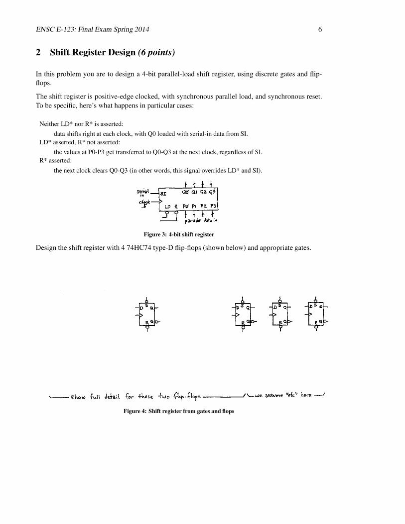
2 Shift Register Design (6 points)
In this problem you are to design a 4-bit parallel-load shift register, using discrete gates and flip-flops.
The shift register is positive-edge clocked, with synchronous parallel load, and synchronous reset.To be specific, here’s what happens in particular cases:
Neither LD* nor R* is asserted:
data shifts right at each clock, with Q0 loaded with serial-in data from SI.LD* asserted, R* not asserted:
the values at P0-P3 get transferred to Q0-Q3 at the next clock, regardless of SI.R* asserted:
the next clock clears Q0-Q3 (in other words, this signal overrides LD* and SI).
Figure 3: 4-bit shift register
Design the shift register with 4 74HC74 type-D flip-flops (shown below) and appropriate gates.
Figure 4: Shift register from gates and flops
ENSC E-123: Final Exam Spring 2014 7
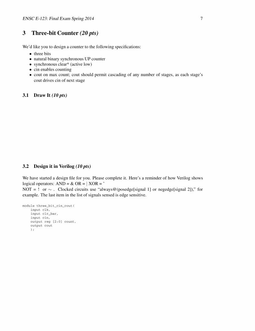
3 Three-bit Counter (20 pts)
We’d like you to design a counter to the following specifications:
• three bits• natural binary synchronous UP counter• synchronous clear* (active low)• cin enables counting• cout on max count; cout should permit cascading of any number of stages, as each stage’s
cout drives cin of next stage
3.1 Draw It (10 pts)
3.2 Design it in Verilog (10 pts)
We have started a design file for you. Please complete it. Here’s a reminder of how Verilog showslogical operators: AND = & OR = | XOR = ˆNOT = ! or ∼ . Clocked circuits use “always@(posedge[signal 1] or negedge[signal 2]),” forexample. The last item in the list of signals sensed is edge sensitive.
module three_bit_cin_cout(input clk,input clr_bar,input cin,output reg [2:0] count,output cout);

ENSC E-123: Final Exam Spring 2014 8
4 Sampling (9 pts)
Your task is to choose some sampling characteristics for a controller with an ADC. We’ll ask youabout these characteristics, one by one.
4.1 Resolution (4 pts)
The ADC in the controller provides ten bits of resolution. Its range is 0V to 2.046V.
If your measurements indicate that your system has noise amplitude (that is, uncertainty in ADCinput) of 5mV peak-to-peak, how many bits can your conversion resolve? (Or, if you prefer, tell ushow many bits of the 10 will be lost to noise). Explain your answer briefly.
4.2 Sampling Rate (5 pts)
You want to acquire signals up to 10kHz and can use the MAX294 filter that you have met in thiscourse, which attenuates to -60dB at 20% above fcutoff (or “f3dB”).
What sampling rate is the minimum that you can safely use? Explain your answer briefly.
ENSC E-123: Final Exam Spring 2014 9
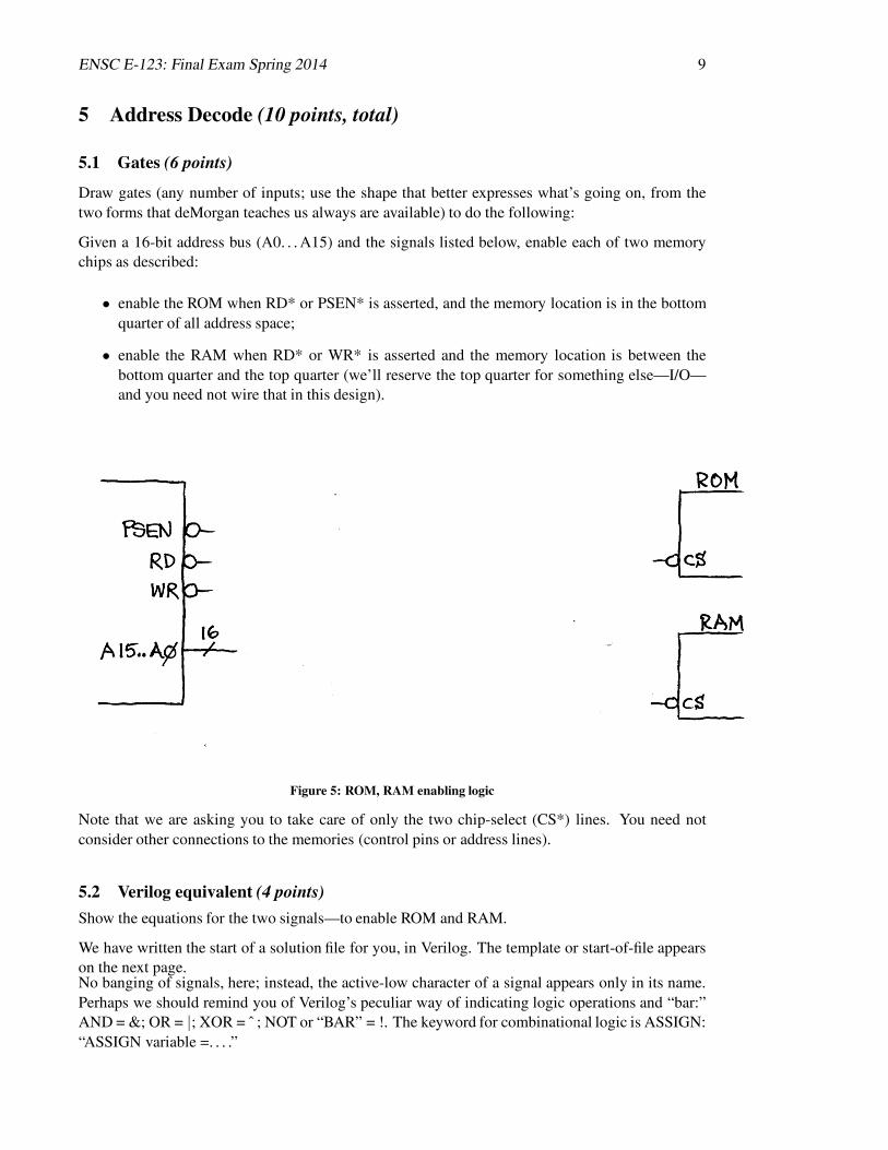
5 Address Decode (10 points, total)
5.1 Gates (6 points)
Draw gates (any number of inputs; use the shape that better expresses what’s going on, from thetwo forms that deMorgan teaches us always are available) to do the following:
Given a 16-bit address bus (A0. . .A15) and the signals listed below, enable each of two memorychips as described:
• enable the ROM when RD* or PSEN* is asserted, and the memory location is in the bottomquarter of all address space;
• enable the RAM when RD* or WR* is asserted and the memory location is between thebottom quarter and the top quarter (we’ll reserve the top quarter for something else—I/O—and you need not wire that in this design).
Figure 5: ROM, RAM enabling logic
Note that we are asking you to take care of only the two chip-select (CS*) lines. You need notconsider other connections to the memories (control pins or address lines).
5.2 Verilog equivalent (4 points)
Show the equations for the two signals—to enable ROM and RAM.
We have written the start of a solution file for you, in Verilog. The template or start-of-file appearson the next page.No banging of signals, here; instead, the active-low character of a signal appears only in its name.Perhaps we should remind you of Verilog’s peculiar way of indicating logic operations and “bar:”AND = &; OR = |; XOR = ˆ ; NOT or “BAR” = !. The keyword for combinational logic is ASSIGN:“ASSIGN variable =. . . .”

ENSC E-123: Final Exam Spring 2014 10
‘timescale 1ns / 1ps//////////////////////////////////////////////////////////////////////////////////// Company: Gearloose// Engineer: You// Create Date: 12:04:05 05/12/2009// Module Name: adr_decode_may09//////////////////////////////////////////////////////////////////////////////////module adr_decode_may09(
input RD_bar,input PSEN_bar,input WR_bar,input A15,input A14,output ROMEN_bar,output RAMEN_bar);

ENSC E-123: Final Exam Spring 2014 11
6 Small Micro I/O Tasks: hardware (8 points, total of those below)
We’d like you to show how to let two switches talk to the 8051, and how to let the 8051 drive twoloads. First, we’ll ask you to do this using built-in ports, then using buses.
6.1 . . . using 8051’s Built-in Ports (4 points)
You will find I/O specification for the 8051 in a summary sheet at the end of this exam (but you mayrecall enough so you’ll not need to consult it). Don’t worry about switch bounce. The motor passes1A @ 10V.
Figure 6: I/O using built-in ports
6.2 . . . using 8051 with external buses (4 points)
Don’t worry about switch bounce. And here we’ll omit the motor, not to make you draw one thingtwice.
Figure 7: I/O using external buses

ENSC E-123: Final Exam Spring 2014 12
7 Small Micro I/O Tasks: Code (11 points, total of those below)
7.1 . . . using 8051’s Built-in Ports (6 points, total of those below)
Write an endless loop that (foolishly) let’s the upper switch control the motor, the lower switchcontrol the LED.1
Do this two ways:
7.1.1 Assume it’s OK to transfer an entire byte (2 points)
This code will alter the levels of the 6 unused output bits at Port1. But that’s OK.
7.1.2 Assume it’s not OK to transfer an entire byte (4 points)
This time, you must leave the 6 unused output bits at Port1 untouched.
7.2 . . . using external bus (5 points
Write an endless loop that (again foolishly) let’s the upper switch control the motor, the lower switchcontrol the LED. We didn’t ask you to draw the motor in the hardware exercise § ?? on page ??; butassume it is present.
Assume it’s OK to transfer an entire byte. This code assumes the hardware you showed in § 6.2 onthe previous page, putting in and out at Port 1 (external buses), data lines d0 and d1, assigned as youplease.
1Yes, we agree: it would be simpler to omit the 8051! But we’re just warming up; you know that the 8051 could beused to make some decisions, so as to justify its inclusion.
ENSC E-123: Final Exam Spring 2014 13
8 Kentucky Derby Circuits (29 pts, total)
Hardware (15 pts, total)
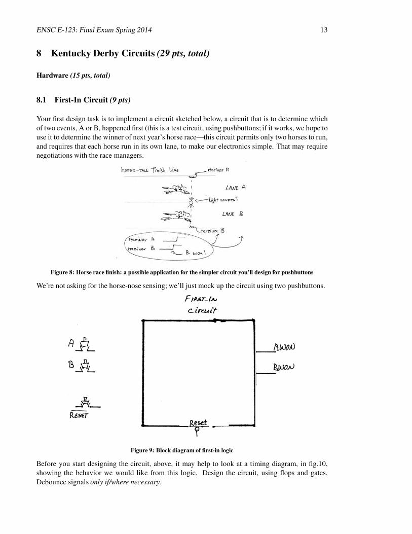
8.1 First-In Circuit (9 pts)
Your first design task is to implement a circuit sketched below, a circuit that is to determine whichof two events, A or B, happened first (this is a test circuit, using pushbuttons; if it works, we hope touse it to determine the winner of next year’s horse race—this circuit permits only two horses to run,and requires that each horse run in its own lane, to make our electronics simple. That may requirenegotiations with the race managers.
Figure 8: Horse race finish: a possible application for the simpler circuit you’ll design for pushbuttons
We’re not asking for the horse-nose sensing; we’ll just mock up the circuit using two pushbuttons.
Figure 9: Block diagram of first-in logic
Before you start designing the circuit, above, it may help to look at a timing diagram, in fig.10,showing the behavior we would like from this logic. Design the circuit, using flops and gates.Debounce signals only if/where necessary.

ENSC E-123: Final Exam Spring 2014 14
Figure 10: Timing diagram showing how first-in logic should respond to signals A and B
8.2 Apply the circuit to controller: Hardware, external buses 3 pts)
Assume the first-in logic is done. Show how to let the 8051 input the who-won information usingexternal buses, at port 1, data lines 0 for A WON, 1 for B WON. Assume I/O decoding has beendone for you, as in the lab Big Board computer.
Figure 11: Winner logic interfaced to 8051 using external buses
8.3 Apply the circuit to controller: Hardware, built-in 8051 port (1 pt)
Assume the first-in logic is done. Show how to let the 8051 input the who-won information usingthe 8051’s built-in PORT0 (P0), using P0,0 for A WON, P0.1 for B WON.2
Figure 12: Winner logic interfaced to 8051 using built-in Port 0 (P0)
2In case you’re a Big Board veteran, worried that Port0 is used for buses; don’t worry: assume that this computer isnot wired to use buses.
ENSC E-123: Final Exam Spring 2014 15
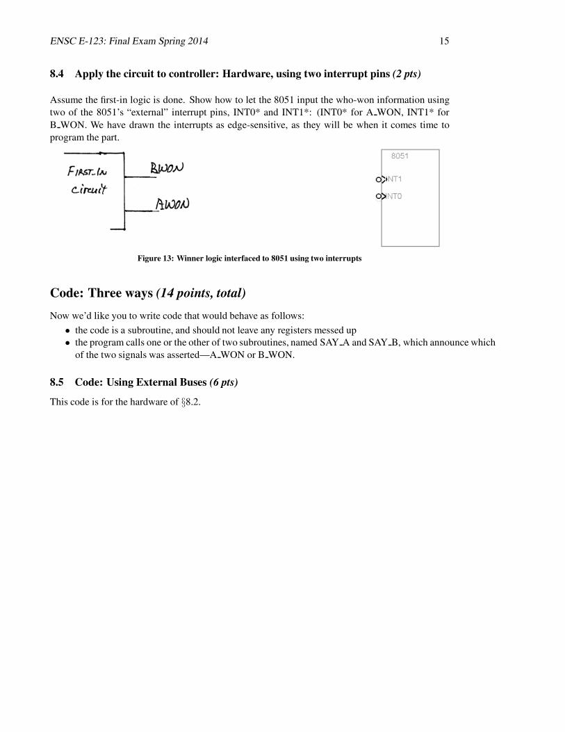
8.4 Apply the circuit to controller: Hardware, using two interrupt pins (2 pts)
Assume the first-in logic is done. Show how to let the 8051 input the who-won information usingtwo of the 8051’s “external” interrupt pins, INT0* and INT1*: (INT0* for A WON, INT1* forB WON. We have drawn the interrupts as edge-sensitive, as they will be when it comes time toprogram the part.
Figure 13: Winner logic interfaced to 8051 using two interrupts
Code: Three ways (14 points, total)
Now we’d like you to write code that would behave as follows:
• the code is a subroutine, and should not leave any registers messed up• the program calls one or the other of two subroutines, named SAY A and SAY B, which announce which
of the two signals was asserted—A WON or B WON.
8.5 Code: Using External Buses (6 pts)
This code is for the hardware of §8.2.

ENSC E-123: Final Exam Spring 2014 16
8.6 Code: Using Built-in Port (3 pts)
This code is for the hardware of §8.3.
8.7 Code: Using Interrupts (5 pts)
This code is for the hardware of §8.4.The winner’s interrupt service response (ISR) should call SAY A or SAY B, appropriately—and should disablethe loser’s interrupt response.Here is the interrupt setup code done in the Main program:
; ----NOW SET UP INTERRUPTS----INT_INITS: setb IT0 ; make INT0 Edge-sensitive (p. 22)
setb IT1 ; ditto for INT1setb EX0 ; ...and enable INT0setb EX1 ; ...and INT1setb EA ; Global int enable (pp.31-32)
ret
End Exam Questions: Appendix followsxb final may2014.tex;May 15, 2014
ENSC E-123: Final Exam Spring 2014 17
Appendix
Sketchy Data Sheets
• 8051 port specifications
• some common 8051 assembly language operations
ENSC E-123: Final Exam Spring 2014 18
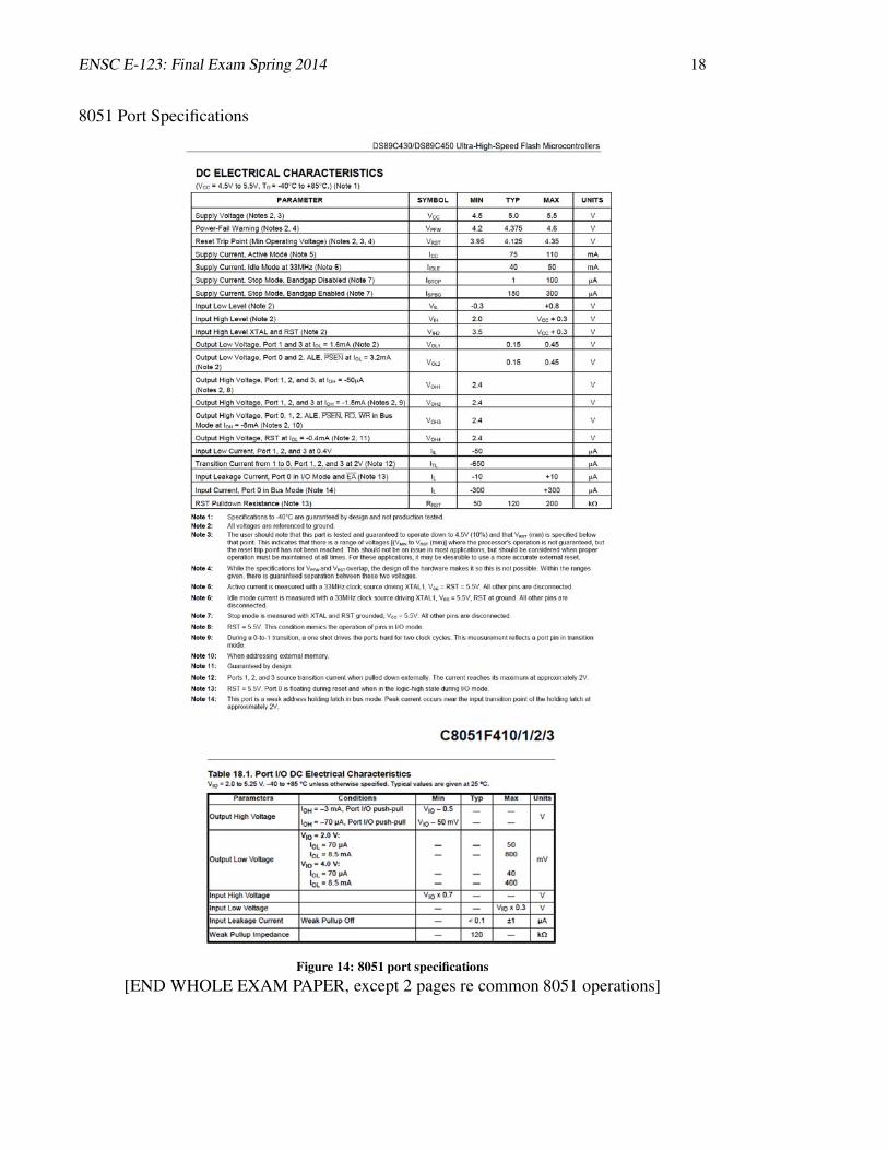
8051 Port Specifications
Figure 14: 8051 port specifications
[END WHOLE EXAM PAPER, except 2 pages re common 8051 operations]

8051: A few of our favorite thingsinspired (one might say, 'shamed') by Carlos, who wrote another, better list--which we hope he'll share with you
5/7/2004, 12/8/05
Addressing Modes example explanationImportant 8051
Resources
"@DPTR" "MOVX @DPTR,A"copies contents of A register (8051 on-chip) to location pointed to by DPTR: that is, to location whose address DPTR holds DPTR
16-bit register on micro. Used to define address of operations between micro and off-chip resources such as RAM or I/O.
To use this instruction, one must first load the appropriate address into DPTR
MOV DPTR, #8003hputs the value 8003h into DPTR: "#" means "immediate," or "use this value; don't go off to location 8003 to get something"
DPS
Dallas provides two DPTRS. They are distinguished only by whether a single bit, DPS, is high or low.
"@R0" MOVX @R0,Acopies contents of A to address whose low-byte is in register R0. The high-byte is provided by Port 2 (on-chip P2).
MOV P2, #80hTo use the `movx @r0,a" instruction, one must first load the appropriate high-byte into P2. Code to left shows that operation. SP
8-bit stack pointer register: used in all forms of CALL, and in PUSH and POP
Operations often used stack
RAM area (on-chip RAM) pointed to by SP. Must be in 'indirectly-addressable' section of RAM.
MOV MOV P2, R3copies contents of register R3 into the on-chip port register P2 (8 flops that can drive Port 2's 8 lines)
A
the privileged 8-bit register: the only location used in MOVX operations. Most arithmetic and logical operations must work on A and another operand; result goes to A.
MOVX MOVX A, @DPTR
see above. The "X" in MOVX means "external," and appears in all transfers between the processor and the outside world, when using the external buses . This is in contrast to use of the built-in ports . The instruction on the line just above, MOV P2, R3 illustrates that contrasting case: a write to a built-in port.
Annoying detail: sometimes A must be referred to as "ACC". For example, in bitoperations: "JNB ACC.7" and in "PUSH ACC."
ADD two flavors of ADD: one takes in the Carry flag, the other doesn't.
ADDC ADDC A, R2forms sum of A and register R2 and the Carry bit (added in at LSB). Result goes into A (hence the name, "accumulator").
SUBB SUBB A, #80h
subtracts the value 80h from A--including a borrow if Carry flag is set. (Carry and Borrow flag are the same bit: same thing.) Result goes to A. The result in A will NOT be a negative number (that would require use of 2's-complement). Use CY flag to determine whether A<#80h--you must have cleared the CY flag before doing the SUBB, n.b., to make this an honest test.
PUSH, POP PUSH ACC, POP ACCstores register contents on stack (only bytes: there is no "PUSH DPTR") . Note funny names: not "A" but "ACC".
Bit Operations
JB, JNB JB P3.4,hangup
test the specified bit--here, bit 4 of built-in port 3--and hop to label "hangup" if that bit is High. This operation is permitted only on certain on-chip locations: so-called "bit-addressable" region, 128 bits between 20h and 2Fh, plus a few others including SFR locations ending in 8 or zero!.
JC, JNC JNC greater_than same as JNB, but looks at the Carry bit
SETB SETB ACC.1 forces a single bit high
CLR CLR P3.0forces a single bit low. Despite the lack of "B" in the mnemonic, this is a BIT operation, except for CLR A, which I think is the only 8-bit clear.
CLR ACPL CPL P3.1 complement (flip)
CPL A flips all 8 bits (but permitted only on A)

Carlos New Improved 8051-programming Reference Summary 5/18/04 COMMANDS What does it mean? THINGS Who the hell is that? INC [] Increments [] # Just the number, not the value DEC [] Decrements [] xxxxh A hex number CPL [] Complements [] (flips it 0↔1) A Accumulator = privileged register CLR [] Clears [] (Makes it LOW (=00)) B Another privileged register SETB [] Sets this bit, [], HIGH (=1) @ At the address the thing points SJMP label Short Jump to a labeled section DPTR Data pointer
AJMP label Absolute Jump to a labeled section. (Longer than SJMP but not as long as LJMP) DPL Main Data pointer low byte
LJMP label Long Jump (the longest) to any section DPH Main Data pointer high byte ACALL label Absolute Call a labeled subroutine DPL1 Alt. data pointer low byte LCALL label Call a labeled subroutine that’s a long way away DPH1 Alt. data pointer high byte JB [], label JB ACC.2, label
Jump to labeled section if this bit, [], is set HIGH. Think: “jump if (this thing is) high” DPS Data Pointer Select; 0 gives 1st, 1 gives 2nd
JNB [], label JNB ACC.4, label
Jump to labeled section if this bit, [], is not HIGH. Think: “jump if (this thing is) low” SP Stack pointer
JC label Jump to label if Carry/Borrow flag is set HIGH. “Jump if Carry (flag is) high.” ACC Another way to say accumulator, used with
DJNZ, JB, JNB, PUSH, POP
JNC label Jump to label if Carry/Borrow flag is Not set HIGH. “Jump if Carry (flag is) low.” Rx Register 0-7
MOV [d], [s] MOV DPTR, #8002h MOV R3, #93h
Internal move, puts source into destination Px.x Port 3, bit 1. These refer to 8051’s internally defined ports
MOVX [d], [s] MOVX A, @DPTR MOVX @DPTR, A
External move, puts source into destination, always into or out of Accumulator ACC.7 7th bit of accumulator
ADD A, [x] if A=81 & Cy=1 or 0 then ADD A, #82h gives A=03, Cy=1
Add x to Acc, put sum into Acc. Does not add the Carry flag at the LSB the way ADDC does. Sets Carry flag HIGH if necessary, otherwise puts it LOW.
C The Carry/Borrow Flag. Sometimes it’s Carry (like with Addition) and sometimes it’s Borrow (like with subtraction)
ADDC A, [x] If Cy=1, A=81 then ADDC A, #82h gives A=04, Cy=1. If Cy was 0, then A=03, Cy=1
Add x to Acc, put sum into Acc, and also add the Carry flag (whether HIGH or LOW) at the LSB. Sets Carry flag HIGH if necessary, otherwise LOW.
ISR
Interrupt Service Routine. On interrupt, program hops to interrupt address (03h for Int0) and executes ISR. Often, just LCALL a subroutine from here.
SUBB A, [x] If Cy is 0 & A=72 then SUBB A, #81 gives A=F1, Cy=1. If Cy was 1, then A=F1, Cy=0
Subtract x from Acc, put results into Acc. Sets the Carry/Borrow flag HIGH if a Borrow is needed for bit 7 (A<x), otherwise, clear Cy flag. Good to clear Cy flag before the first SUBB operation.
SETB EA SETB EX0 SETB IT0
To enable interrupts, do these three things. EA is global interrupt enable. EX0 enables External Interrupt 0. IT0 is a timer control thingy for ext. interrupt 0 that makes it edge sensitive. Could also use interrupt 1 (SETB EX1 and IT1) but let’s keep things simple
DJNZ [], label First: MOV R6, #06h and later: DJNZ R6, label counts down from 06
Decrement [], and then jump to labeled section if result of decrement is not zero. Nice to first load a Rx register with a countdown value
PSW.1 Program Status Word, can use this bit as a general purpose flag
PUSH [] PUSH ACC, PUSH DPH PUSH DPL
Pushes a copy of [] onto the top of the stack so it can be manipulated and thrown out, and the original recovered. A FEW OTHER THINGS
POP [] POP ACC, POP DPH
Pull the original version of [] off the top of the stack, replacing whatever you’ve been handling EQU Gives a name to a location. FLAGNAME EQU 05h
allows you to refer to 05h by the name FLAGNAME RRC A For A=05, Cy=0, RRC A gives A=2, Cy=1. Nice.
Rotates Acc Right thru the Carry flag. Divides Acc by two. Bit 0 goes to Cy flag; original Cy flag goes to bit 7. ORG [xxxx] Origin. Just a start line
RR A For A=04, RR A gives 02. Fine. If A=03, RR A gives 81. Weird.
Rotates Acc Right. Bit 0 goes to bit 7. This is a funny divide-by-two where the remainder, if any, affects high digit. NOP No Operation. Does nothing, just takes up a line
MUL AB A=06, B=02; MUL AB gives A=0C, B=00.
Multiply Acc times B, high byte of product into B, low byte into Acc. Cy flag cleared. DA Decimal Adjust the accumulator
DIV AB A=0D, B=03; DIV AB gives A=04, B=01.
Divides Acc by B. Integer of quotient into Acc, remainder into B. Cy flag cleared. END End of a program
RET Return from a subroutine to the next line in main code
RETI Return from an interrupt to the next line in main code