enhancement in terahertz emission using auge … in terahertz emission using auge nanopatterns ......
TRANSCRIPT
Enhancement in Terahertz Emission using AuGe Nanopatterns
Harshad Surdi, Abhishek Singh, Dr. S.S. Prabhu

Tera… what?
• Terahertz (THz) radiation occupies the electromagnetic spectrum between optical (1015 Hz) and infrared (1013 Hz) frequencies and microwave frequencies (1011 Hz) i.e. wavelength ranges from 0.3mm to 3mm

Applications of THz technology are :

Non-invasive imaging
Water content in a leaf before and after 48 hours.
B. B. Hu and M. C. Nuss “Imaging with terahertz waves”, OPTICS LETTERS / Vol. 20, No. 16 / August 15, 1995

Imaging of explosives
False-colour terahertz chemical maps showing the spatial distributions of lactose scd, sucrose sdd, and
RDX.Y. C. Shen et. al. “Detection and identification of explosives using terahertz pulsed
spectroscopic imaging, APPLIED PHYSICS LETTERS 86, 241116 s2005d

Airport Security
T-Ray imaging at airport security centers to reveal concealed weapon
Spiegel Online, Splitternackt auf dem Monitor

THz Sources

Methods of generating THz radiation
• Photo-conductive Antenna Excitation of photo-carriers by optical wavelengths Acceleration of the photo-carriers to generate
terahertz radiation• Difference frequency generation Mixing of two high frequencies Difference between the mixing frequencies should
lie in the THz range

THz PCA
-10V
+10V
--
- --
--
- --
--
--
--
--

Nano-plasmonics
• Nano-plasmonics deals with the light-matter interaction at very small geometries

Surface Plasmons Polaritons
• Plasmons are collective electron oscillations
• SPPs are a result of the coupling of the incident light’s electromagnetic field to the oscillations of the metal’s electron plasma.

• They follow the following dispersion relation
ba
ba0SPP εε
εεκκ
Surface Plasmons Polaritons
• Where κspp is the momentum of the SPP and κo is the free space vector
cωκ0

• By observing the left hand side of the equation we can see that for a air-dielectric interface, κspp is greater than the left hand side of the equation
• This means we should compensate for the extra momentum in order to excite SPPs from air.
• The metallic grating provides an extra momentum along the direction of the grating
Surface Plasmons Polaritons
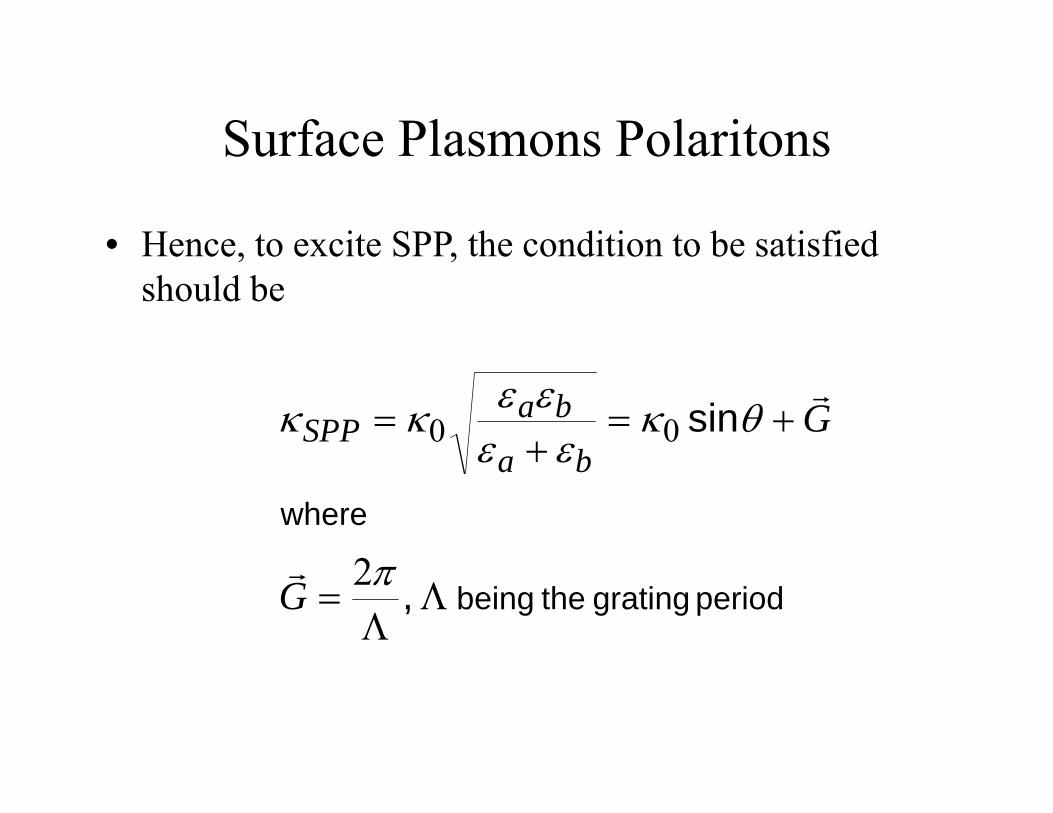
• Hence, to excite SPP, the condition to be satisfied should be
period grating the being
where
,
sin
2
00
G
Gba
baSPP
Surface Plasmons Polaritons
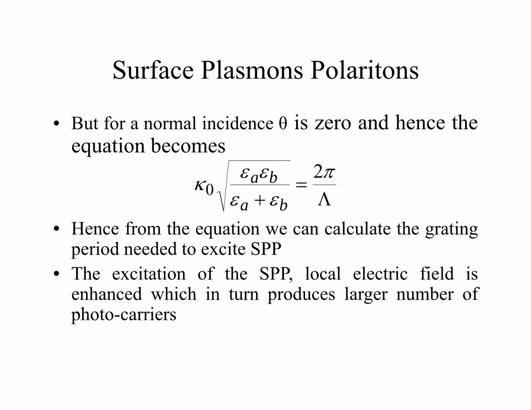
• But for a normal incidence θ is zero and hence theequation becomes
• Hence from the equation we can calculate the gratingperiod needed to excite SPP
• The excitation of the SPP, local electric field isenhanced which in turn produces larger number ofphoto-carriers
2
0ba
ba
Surface Plasmons Polaritons
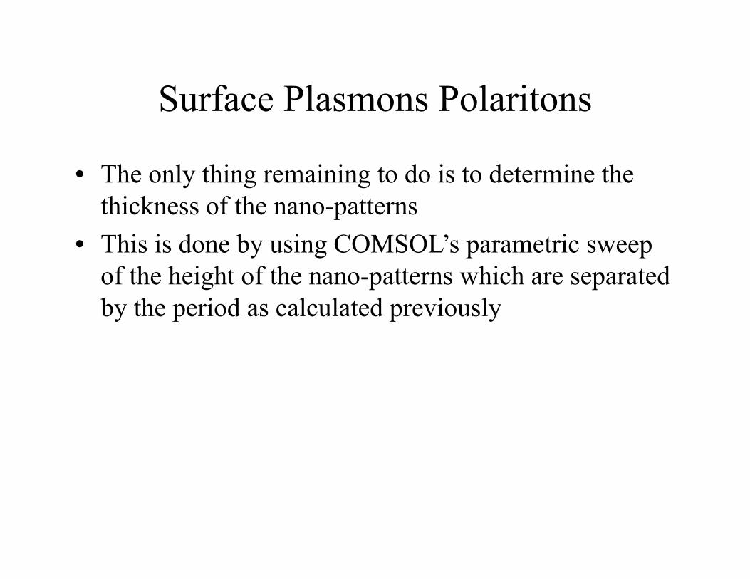
• The only thing remaining to do is to determine the thickness of the nano-patterns
• This is done by using COMSOL’s parametric sweep of the height of the nano-patterns which are separated by the period as calculated previously
Surface Plasmons Polaritons
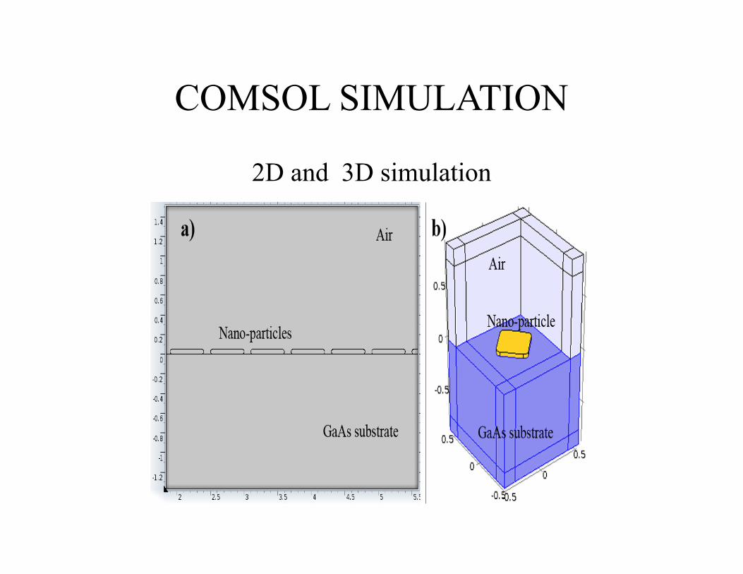
COMSOL SIMULATION
2D and 3D simulation
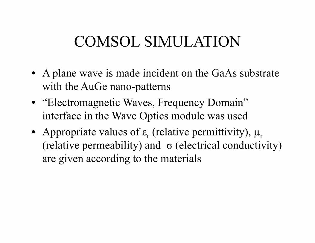
COMSOL SIMULATION
• A plane wave is made incident on the GaAs substrate with the AuGe nano-patterns
• “Electromagnetic Waves, Frequency Domain” interface in the Wave Optics module was used
• Appropriate values of εr (relative permittivity), µr(relative permeability) and σ (electrical conductivity) are given according to the materials
• Parametric Sweep of the height of the nano-patterns is done to find out the optimal height where the local electric field will be maximum
COMSOL SIMULATION
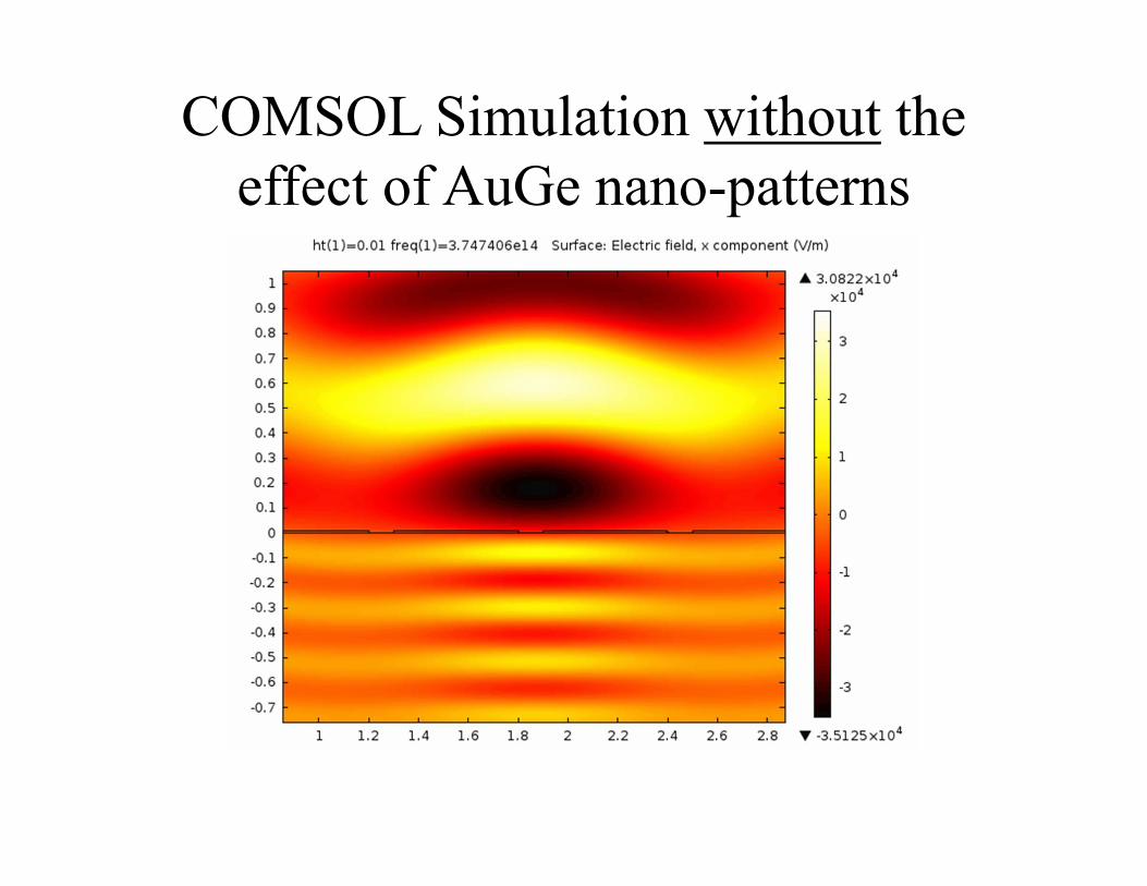
COMSOL Simulation without the effect of AuGe nano-patterns
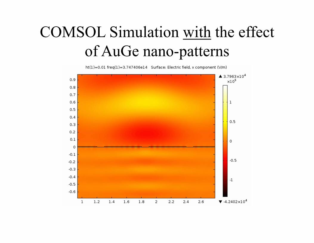
COMSOL Simulation with the effect of AuGe nano-patterns

COMSOL SIMULATION

Fabrication
SI - GaAs

Sputter deposition of 40nm layer of AuGe on GaAssubstrate
SI - GaAs
AuGe

Spin coating the E-beam resist onto the sputtered waffer
SI - GaAs
AuGeE-beam resist

Writing THz antenna pattern with E-beam lithography
SI - GaAs
AuGeE-beam resist
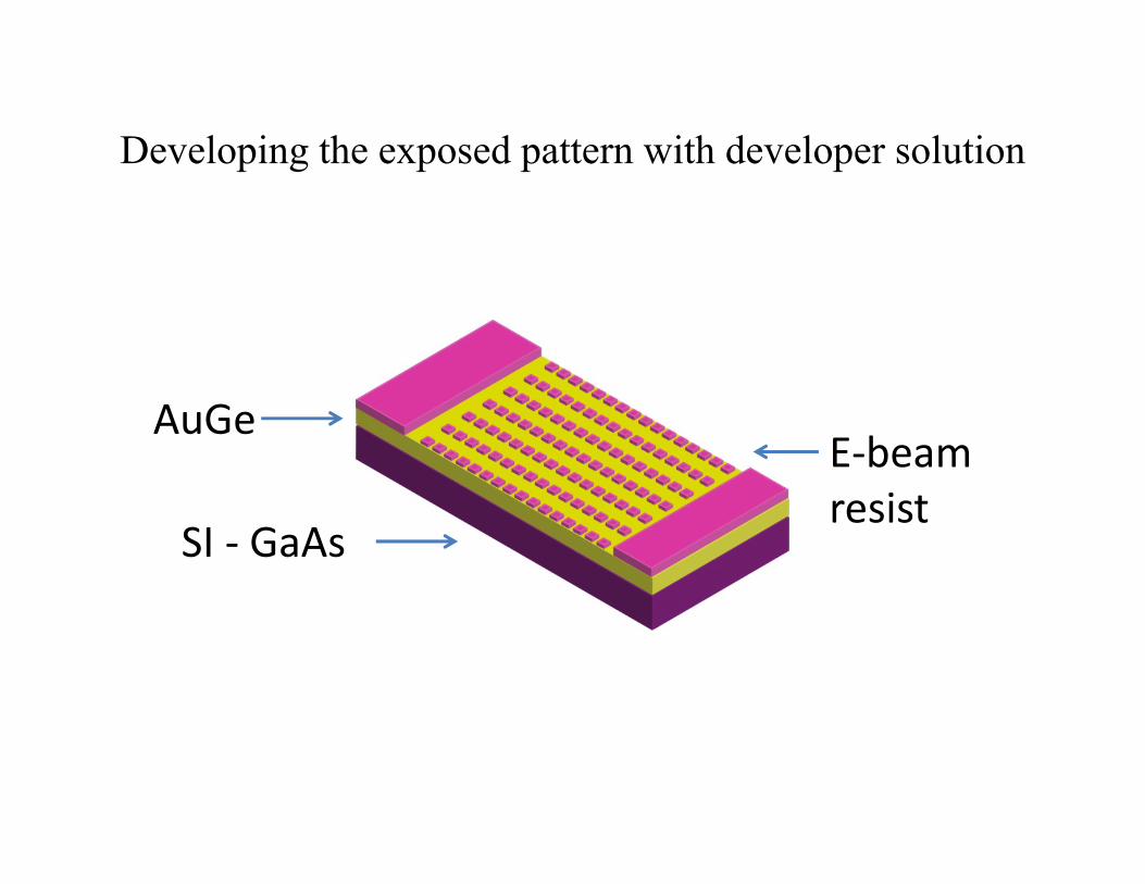
SI - GaAs
AuGeE-beam resist
Developing the exposed pattern with developer solution
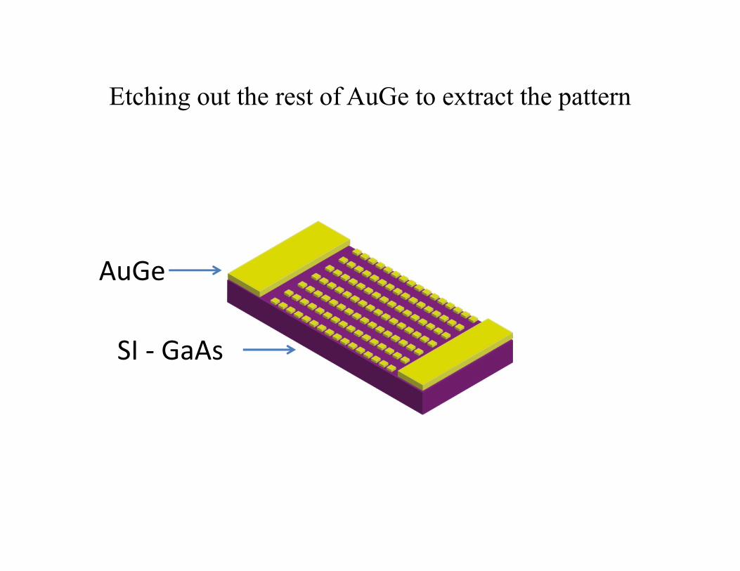
Etching out the rest of AuGe to extract the pattern
SI - GaAs
AuGe
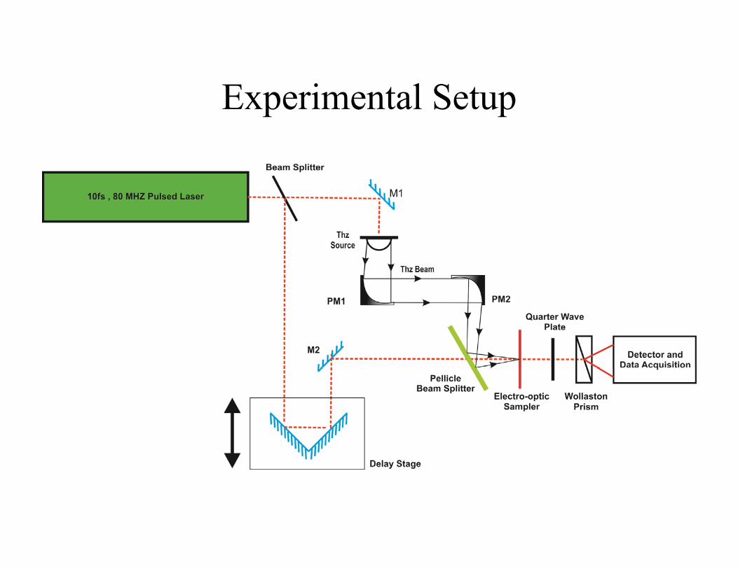
Experimental Setup

Experimental Data
-5 0 5 10 15 20
-0.004
-0.002
0.000
0.002
0.004
0.006
0.008
A
mpl
itude
(a.u
.)
Time (psec)
THz antenna with nano-pattern THz antenna w/o nano-pattern

Experimental Data
0.0 0.5 1.0 1.5 2.0 2.5 3.0 3.5 4.01E-6
1E-5
1E-4
1E-3
Am
plitu
de (a
.u.)
Frequency (THz)
THz antenna with nano-pattern THz antenna w/o nano-pattern

THANK YOU
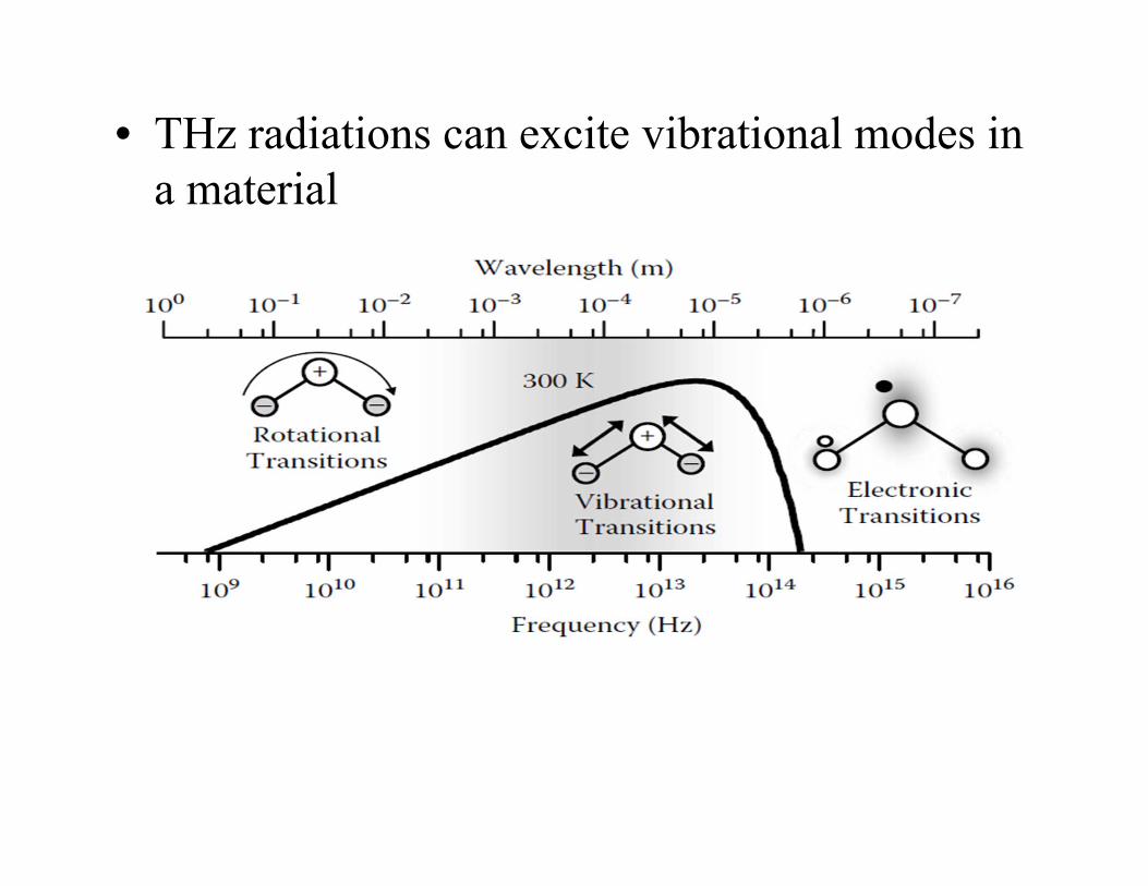
• THz radiations can excite vibrational modes in a material