enhanced broadband and omni-directional performance of...
TRANSCRIPT
Enhanced broadband and omni-directional performance of polycrystalline Si solar cells by using discrete multilayer antireflection coatings
Seung Jae Oh,1 Sameer Chhajed,1 David J. Poxson,2 Jaehee Cho,2 E. Fred Schubert,2 Sung Ju Tark,3 Donghwan Kim,3 and Jong Kyu Kim,1,*
1Department of Materials and Engineering, Pohang University of Science and Technology (POSTECH), Pohang, 790-784, South Korea
2Future Chips Constellation, Department of Electrical, Computer, and Systems Engineering, Rensselaer Polytechnic Institute, Troy, New York 12180, USA
3Department of Materials Science and Engineering, Korea University, Seoul 136-713, South Korea *[email protected]
Abstract: The performance enhancement of polycrystalline Si solar cells by using an optimized discrete multilayer anti-reflection (AR) coating with broadband and omni-directional characteristics is presented. Discrete multilayer AR coatings are optimized by a genetic algorithm, and experimentally demonstrated by refractive-index tunable SiO2 nano-helix arrays and co-sputtered (SiO2)x(TiO2)1-x thin film layers. The optimized multilayer AR coating shows a reduced total reflection, leading to the high incident-photon-to-electron conversion efficiency over a correspondingly wide range of wavelengths and incident angles, offering a very promising way to harvest more solar energy by virtually any type of solar cells for a longer time of a day.
©2012 Optical Society of America
OCIS codes: (310.1210) Antireflection coatings; (310.4165) Multilayer design; (310.6628) Subwavelength structures, nanostructures; (040.5350) Photovoltaic.
References and links
1. J. Zhao and M. A. Green, “Optimized antireflection coatings for high-efficiency silicon solar cells,” IEEE Trans. Electron. Dev. 38(8), 1925–1934 (1991).
2. L. Schirone, G. Sotgiu, and F. P. Califano, “Chemically etched porous silicon as an anti-reflection coating for high efficiency solar cells,” Thin Solid Films 297(1-2), 296–298 (1997).
3. J. S. Rayleigh, “On reflection of vibrations at the confines of two media between which the transition is gradual,” Proc. Lond. Math. Soc. S11(1), 51–56 (1879).
4. Y.-A. Dai, H.-C. Chang, K.-Y. Lai, C.-A. Lin, R.-J. Chung, G.-R. Lin, and J.-H. He, “Subwavelength Si nanowire arrays for self-cleaning antireflection coatings,” J. Mater. Chem. 20(48), 10924–10930 (2010).
5. C. C. Striemer and P. M. Fauchet, “Dynamic etching of silicon for broadband antireflection applications,” Appl. Phys. Lett. 81(16), 2980–2982 (2002).
6. J. Zhu, Z. Yu, G. F. Burkhard, C.-M. Hsu, S. T. Connor, Y. Xu, Q. Wang, M. McGehee, S. Fan, and Y. Cui, “Optical absorption enhancement in amorphous silicon nanowire and nanocone arrays,” Nano Lett. 9(1), 279–282 (2009).
7. C. Lee, S. Y. Bae, S. Mobasser, and H. Manohara, “A Novel Silicon Nanotips Antireflection Surface for the Micro Sun Sensor,” Nano Lett. 5(12), 2438–2442 (2005).
8. Y. F. Huang, S. Chattopadhyay, Y. J. Jen, C. Y. Peng, T. A. Liu, Y. K. Hsu, C. L. Pan, H. C. Lo, C. H. Hsu, Y. H. Chang, C. S. Lee, K. H. Chen, and L. C. Chen, “Improved broadband and quasi-omnidirectional anti-reflection properties with biomimetic silicon nanostructures,” Nat. Nanotechnol. 2(12), 770–774 (2007).
9. K. Hadobás, S. Kirsch, A. Carl, M. Acet, and E. F. Wassermann, “Reflection properties of nanostructure-arrayed silicon surfaces,” Nanotechnology 11(3), 161–164 (2000).
10. Y. Kanamori, M. Sasaki, and K. Hane, “Broadband antireflection gratings fabricated upon silicon substrates,” Opt. Lett. 24(20), 1422–1424 (1999).
11. Y. J. Lee, D. S. Ruby, D. W. Peters, B. B. McKenzie, and J. W. P. Hsu, “ZnO nanostructures as efficient antireflection layers in solar cells,” Nano Lett. 8(5), 1501–1505 (2008).
12. S. Hyun Lee, G. Earle Jellison, C. E. Duty, and J. Xu, “Light confinement-induced antireflection of ZnO nanocones,” Appl. Phys. Lett. 99(15), 153113 (2011).
#173581 - $15.00 USD Received 31 Jul 2012; revised 29 Nov 2012; accepted 29 Nov 2012; published 17 Dec 2012(C) 2012 OSA 14 January 2013 / Vol. 21, No. S1 / OPTICS EXPRESS A157
13. Y.-C. Chao, C.-Y. Chen, C.-A. Lin, and J.-H. He, “Light scattering by nanostructured anti-reflection coatings,” Energy and Environ. Sci. 4(9), 3436–3441 (2011).
14. M. F. Schubert, D. J. Poxson, F. W. Mont, J. K. Kim, and E. F. Schubert, “Performance of antireflection coatings consisting of multiple discrete layers and comparison with continuously graded antireflection coatings,” Appl. Phys. Express 3(8), 082502 (2010).
15. J. Q. Xi, M. F. Schubert, J. K. Kim, E. F. Schubert, M. Chen, S. Y. Lin, W. Liu, and J. A. Smart, “Optical thin-film materials with low refractive index for broadband elimination of Fresnel reflection,” Nat. Photonics 1, 176–179 (2007).
16. J. K. Kim, S. Chhajed, M. F. Schubert, E. F. Schubert, A. J. Fischer, M. H. Crawford, J. Cho, H. Kim, and C. Sone, “Light-extraction enhancement of GaInN light-emitting diodes by graded-refractive-index indium tin oxide anti-reflection contact,” Adv. Mater. (Deerfield Beach Fla.) 20(4), 801–804 (2008).
17. P. Yu, C.-H. Chang, C.-H. Chiu, C.-S. Yang, J.-C. Yu, H.-C. Kuo, S.-H. Hsu, and Y.-C. Chang, “Efficiency enhancement of GaAs photovoltaics employing antireflective indium tin oxide nanocolumns,” Adv. Mater. (Deerfield Beach Fla.) 21(16), 1618–1621 (2009).
18. S. Chhajed, M. F. Schubert, J. K. Kim, and E. F. Schubert, “Nanostructured multilayer graded-index antireflection coating for Si solar cells with broadband and omnidirectional characteristics,” Appl. Phys. Lett. 93(25), 251108 (2008).
19. D. J. Poxson, M. F. Schubert, F. W. Mont, E. F. Schubert, and J. K. Kim, “Broadband omnidirectional antireflection coatings optimized by genetic algorithm,” Opt. Lett. 34(6), 728–730 (2009).
20. D. J. Poxson, M.-L. Kuo, F. W. Mont, Y.-S. Kim, X. Yan, R. E. Welser, A. K. Sood, J. Cho, S.-Y. Lin, and E. F. Schubert, “High-performance antireflection coatings utilizing nanoporous layers,” MRS Bull. 36(06), 434–438 (2011).
21. M. F. Schubert, F. W. Mont, S. Chhajed, D. J. Poxson, J. K. Kim, and E. F. Schubert, “Design of multilayer antireflection coatings made from co-sputtered and low-refractive-index materials by genetic algorithm,” Opt. Express 16(8), 5290–5298 (2008).
22. S. Chhajed, D. J. Poxson, X. Yan, J. Cho, E. F. Schubert, R. E. Welser, A. K. Sood, and J. K. Kim, “Nanostructured multilayer tailored-refractive-index antireflection coating for glass with broadband and omnidirectional characteristics,” Appl. Phys. Express 4(5), 052503 (2011).
23. S. V. Nitta, V. Pisupatti, A. Jain, P. C. Wayner, Jr., W. N. Gill, and J. L. Plawsky, “Surface modified spin on xerogel films as interlayer dielectrics,” J. Vac. Sci. Technol. B 17(1), 205–212 (1999).
24. J. Q. Xi, M. Ojha, J. L. Plawsky, W. N. Gill, J. K. Kim, and E. F. Schubert, “Internal high-reflectivity omni-directional reflectors,” Appl. Phys. Lett. 87(3), 031111 (2005).
25. L. Abelmann and C. Lodder, “Oblique evaporation and surface diffusion,” Thin Solid Films 305(1-2), 1–21 (1997).
26. D. A. G. Bruggeman, “Berechnung verschiedener physikalischer Konstanten von heterogenen Substanzen. I. Dielektrizitätskonstanten und Leitfähigkeiten der Mischkörper aus isotropen Substanzen,” Annalen der Physik 416(7), 636–664 (1935).
27. A. M. Goodman, “Optical interference method for the approximate determination of refractive index and thickness of a transparent layer,” Appl. Opt. 17(17), 2779–2787 (1978).
28. M. Khardani, M. Bouaïcha, and B. Bessaïs, “Bruggeman effective medium approach for modelling optical properties of porous silicon: comparison with experiment,” Phys. Status Solidi., C Curr. Top. Solid State Phys. 4(6), 1986–1990 (2007).
1. Introduction
Anti-reflection (AR) coatings are widely used in many optoelectronic devices and systems to reduce unwanted optical reflections. In particular, AR coatings for solar cells are very beneficial to minimize the reflection loss, thus, to increase the power conversion efficiency of solar cells [1, 2]. For conventional single- and double-layer AR coatings, the thickness and the refractive index are chosen to insure that as the normal incident light wave with a specific wavelength strikes the solar cell, the reflected light wave destructively interferes with the incident light wave. However, there is a fundamental limitation of such conventional AR coatings - although the reflection loss is minimal near the wavelength and the angle of incidence where they are optimized, it increases drastically for other wavelengths and angles of incidence. Since the solar irradiance is inherently broadband and its angle of incidence is wide due to the diffuse light scattered by the atmosphere and the positional variation of the sun during the course of a day and during the course of the seasons. AR coatings having low reflection over a wide range of wavelengths and angles of incidence, i.e., broadband and omni-directional characteristics, are highly desirable to harvest more solar energy for a longer time of the day.
#173581 - $15.00 USD Received 31 Jul 2012; revised 29 Nov 2012; accepted 29 Nov 2012; published 17 Dec 2012(C) 2012 OSA 14 January 2013 / Vol. 21, No. S1 / OPTICS EXPRESS A158
More than 130 years ago, it was theoretically demonstrated that an optical medium with a continuously graded refractive-index profile can effectively reduce the reflection for wide range of wavelengths and incident angles [3]. In order to realize such continuous refractive-index-graded coatings, various bottom-up and top-down approaches have been developed [4–10]. As top-down approaches, moth-eye structures fabricated by wet [4, 5], dry etching [6–8] or electron-beam lithography patterned dielectrics [9, 10] were reported to have broadband and omni-directional characteristics due to the continuously-graded refractive-index profile enabled by the array of needle-like individual nanostructures. However, such top-down etching approaches require thicker (up to several micrometers) starting material to be etched, thus wasted, than needed for the active region of solar cells, and additional process steps such as lithography and/or protection layer deposition for etching process. Moreover, such approaches could be implemented only for a specific solar cell material through an proper etching process suitable for the material. On the other hand, a number of bottom-up approaches, including ZnO nanowire arrays grown by chemical vapor deposition or hydrothermal process have been reported to show favorable AR characteristics [11–13].
Recently, it was reported that appropriately designed discrete multilayer AR coatings can outperform any continuously-graded AR coatings by taking advantage of the interference effect [14]. Due to the oblique-angle deposition (OAD) technique, with which the refractive index of thin film can be precisely tuned to a desired value (down to about 1.1) [15], such discrete multilayer coatings were recently demonstrated on various semiconductor substrates including AlN [15], GaN [16], GaAs [17] and Si [18–20]. The OAD is a very promising method for producing ordered nanostructure arrays of a variety of materials with excellent refractive-index tunability, position/shape-controllability, reproducibility, and compatibility with conventional micro-electronics processes at a low cost [18]. Despite the great potential of discrete multilayer AR coatings for broadband and omni-directional AR coatings, no report demonstrating an enhancement of the efficiency in commercial solar cells with such AR coatings has been reported.
In this study, we present an enhanced performance of commercial polycrystalline Si solar cells by using discrete multilayer AR coatings. By taking advantage of tunable- and low-refractive index materials offered by co-sputtering and OAD methods, an optimized 4-layer AR coating was designed by a genetic algorithm (GA) and fabricated on a polycrystalline Si solar cell. The excellent broadband and omni-directional characteristics of the GA-optimized AR coatings are demonstrated, which directly lead to an enhanced power conversion efficiency of polycrystalline Si solar cells.
2. Optimization of AR coatings
Discrete multilayer AR coatings optimized by using GA have been reported in the literature [19, 21]. Starting from a given number of layers, the optimization algorithm creates a random population of potential AR structures of various layer thicknesses and indices of refraction, and then determines the fitness of each structure against a figure of merit (FOM). A fraction of the worst performing structures is discarded and replaced with the genetic “offspring” of two randomly chosen remaining “parents” (‘fit’ structures), which is repeated until good convergence on the design parameters of the population is achieved. One of the advantages of this optimization scheme is the great flexibility of the user defined conditions - for example, ranges of wavelengths and angles of incidence, the absorption characteristic of any solar cell material, and weighting factors concerning the relative importance of specific conditions, etc. - for an optimal structure.
In this study, we set air as the ambient surrounding the Si solar cell, thus, boundary conditions for the GA optimization include the highest and the lowest refractive indices of 2.4 and 1.1 at λ = 550nm, experimentally acquired from bulk TiO2 and nanoporous SiO2 fabricated by OAD, respectively. Note that in practical situation where solar cells are encapsulated by EVA and cover glass, boundary conditions in the GA optimization should be
#173581 - $15.00 USD Received 31 Jul 2012; revised 29 Nov 2012; accepted 29 Nov 2012; published 17 Dec 2012(C) 2012 OSA 14 January 2013 / Vol. 21, No. S1 / OPTICS EXPRESS A159
modified accordingly and the reflection loss at the air-cover glass interface can be reduced by another optimized multilayer AR coating on top of the cover glass [22].
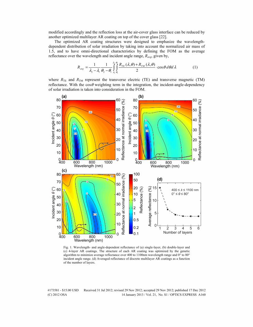
The optimized AR coating structures were designed to emphasize the wavelength-dependent distribution of solar irradiation by taking into account the normalized air mass of 1.5, and to have omni-directional characteristics by defining the FOM as the average reflectance over the wavelength and incident angle range, Ravg, given by,
2 2
1 12 1 2 1
( , ) ( , )1 1cos
2TE TM
avg
R RR d d
λ θ
λ θ
λ θ λ θ θ θ λλ λ θ θ
+= ⋅
− − (1)
where RTE and RTM represent the transverse electric (TE) and transverse magnetic (TM) reflectance. With the cosθ weighting term in the integration, the incident-angle-dependency of solar irradiation is taken into consideration in the FOM.
Fig. 1. Wavelength- and angle-dependent reflectance of (a) single-layer, (b) double-layer and (c) 4-layer AR coatings. The structure of each AR coating was optimized by the genetic algorithm to minimize average reflectance over 400 to 1100nm wavelength range and 0° to 80° incident angle range. (d) Averaged reflectance of discrete multilayer AR coatings as a function of the number of layers.
#173581 - $15.00 USD Received 31 Jul 2012; revised 29 Nov 2012; accepted 29 Nov 2012; published 17 Dec 2012(C) 2012 OSA 14 January 2013 / Vol. 21, No. S1 / OPTICS EXPRESS A160
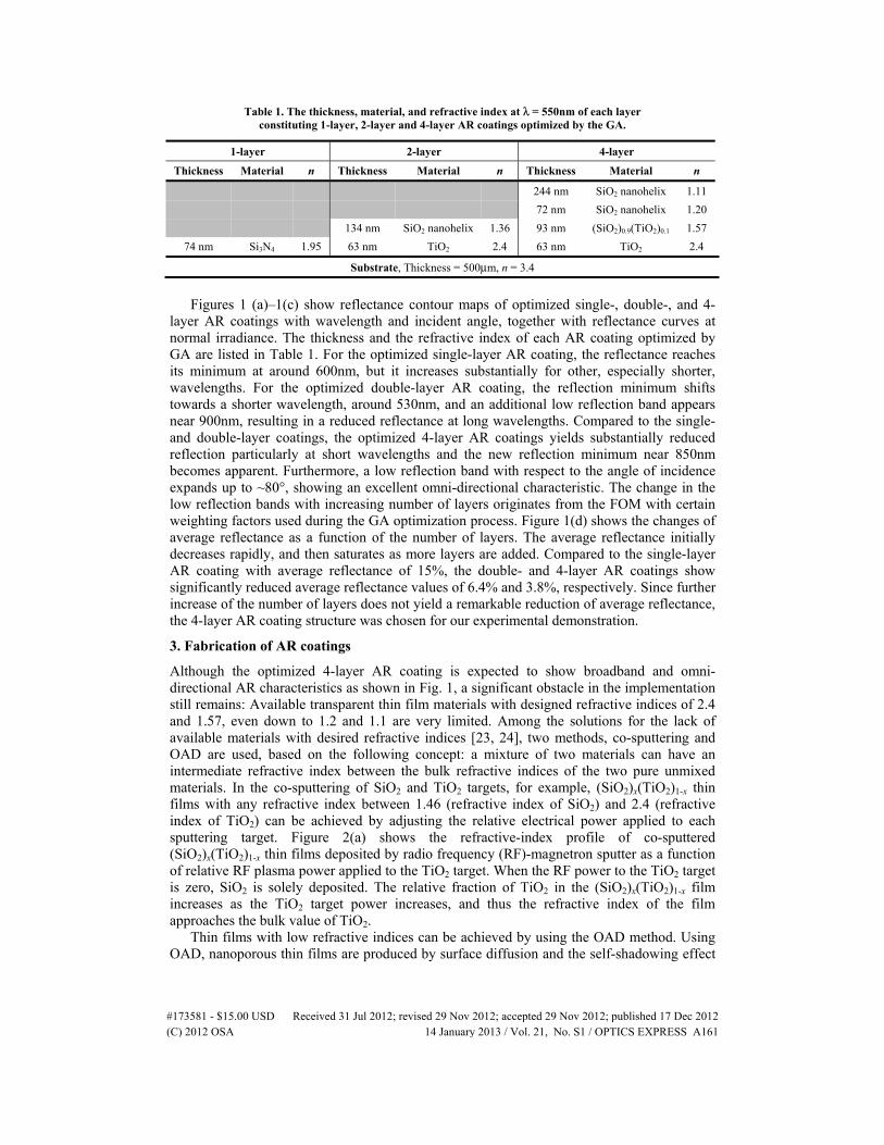
Table 1. The thickness, material, and refractive index at λ = 550nm of each layer constituting 1-layer, 2-layer and 4-layer AR coatings optimized by the GA.
1-layer 2-layer 4-layer
Thickness Material n Thickness Material n Thickness Material n
244 nm SiO2 nanohelix 1.11
72 nm SiO2 nanohelix 1.20
134 nm SiO2 nanohelix 1.36 93 nm (SiO2)0.9(TiO2)0.1 1.57
74 nm Si3N4 1.95 63 nm TiO2 2.4 63 nm TiO2 2.4
Substrate, Thickness = 500μm, n = 3.4
Figures 1 (a)–1(c) show reflectance contour maps of optimized single-, double-, and 4-layer AR coatings with wavelength and incident angle, together with reflectance curves at normal irradiance. The thickness and the refractive index of each AR coating optimized by GA are listed in Table 1. For the optimized single-layer AR coating, the reflectance reaches its minimum at around 600nm, but it increases substantially for other, especially shorter, wavelengths. For the optimized double-layer AR coating, the reflection minimum shifts towards a shorter wavelength, around 530nm, and an additional low reflection band appears near 900nm, resulting in a reduced reflectance at long wavelengths. Compared to the single- and double-layer coatings, the optimized 4-layer AR coatings yields substantially reduced reflection particularly at short wavelengths and the new reflection minimum near 850nm becomes apparent. Furthermore, a low reflection band with respect to the angle of incidence expands up to ~80°, showing an excellent omni-directional characteristic. The change in the low reflection bands with increasing number of layers originates from the FOM with certain weighting factors used during the GA optimization process. Figure 1(d) shows the changes of average reflectance as a function of the number of layers. The average reflectance initially decreases rapidly, and then saturates as more layers are added. Compared to the single-layer AR coating with average reflectance of 15%, the double- and 4-layer AR coatings show significantly reduced average reflectance values of 6.4% and 3.8%, respectively. Since further increase of the number of layers does not yield a remarkable reduction of average reflectance, the 4-layer AR coating structure was chosen for our experimental demonstration.
3. Fabrication of AR coatings
Although the optimized 4-layer AR coating is expected to show broadband and omni-directional AR characteristics as shown in Fig. 1, a significant obstacle in the implementation still remains: Available transparent thin film materials with designed refractive indices of 2.4 and 1.57, even down to 1.2 and 1.1 are very limited. Among the solutions for the lack of available materials with desired refractive indices [23, 24], two methods, co-sputtering and OAD are used, based on the following concept: a mixture of two materials can have an intermediate refractive index between the bulk refractive indices of the two pure unmixed materials. In the co-sputtering of SiO2 and TiO2 targets, for example, (SiO2)x(TiO2)1-x thin films with any refractive index between 1.46 (refractive index of SiO2) and 2.4 (refractive index of TiO2) can be achieved by adjusting the relative electrical power applied to each sputtering target. Figure 2(a) shows the refractive-index profile of co-sputtered (SiO2)x(TiO2)1-x thin films deposited by radio frequency (RF)-magnetron sputter as a function of relative RF plasma power applied to the TiO2 target. When the RF power to the TiO2 target is zero, SiO2 is solely deposited. The relative fraction of TiO2 in the (SiO2)x(TiO2)1-x film increases as the TiO2 target power increases, and thus the refractive index of the film approaches the bulk value of TiO2.
Thin films with low refractive indices can be achieved by using the OAD method. Using OAD, nanoporous thin films are produced by surface diffusion and the self-shadowing effect
#173581 - $15.00 USD Received 31 Jul 2012; revised 29 Nov 2012; accepted 29 Nov 2012; published 17 Dec 2012(C) 2012 OSA 14 January 2013 / Vol. 21, No. S1 / OPTICS EXPRESS A161
[25] so that the porosity can be precisely controlled by adjusting the deposition angle. Based on the effective media approximation, nanoporous thin films can have an intermediate refractive index, i.e. between the refractive index of the deposited dense material and that of air, ~1 [26–28]. Figure 2(b) shows the porosity and the refractive index of porous SiO2 thin films deposited by electron-beam evaporation as a function of deposition angle. The refractive index of SiO2 film decreases as the deposition angle increases due to increased porosity. Note that the refractive index of a SiO2 thin film can be precisely tuned from 1.46 (θ = 0°) to 1.1 (θ = 83°) at 550nm.
Fig. 2. (a) Measured refractive index of co-sputtered (SiO2)x(TiO2)1-x thin films as a function of relative RF plasma power applied to the TiO2 target. (b) Measured refractive index and calculated porosity of SiO2 thin films deposited by OAD as a function of deposition angle, θ.
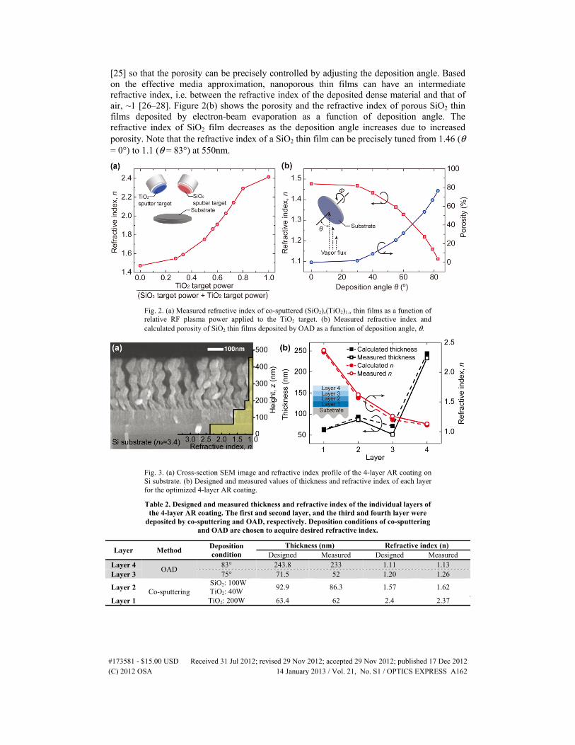
Fig. 3. (a) Cross-section SEM image and refractive index profile of the 4-layer AR coating on Si substrate. (b) Designed and measured values of thickness and refractive index of each layer for the optimized 4-layer AR coating.
Table 2. Designed and measured thickness and refractive index of the individual layers of the 4-layer AR coating. The first and second layer, and the third and fourth layer were
deposited by co-sputtering and OAD, respectively. Deposition conditions of co-sputtering and OAD are chosen to acquire desired refractive index.
Layer Method Deposition condition
Thickness (nm) Refractive index (n) Designed Measured Designed Measured
Layer 4 OAD
83° 243.8 233 1.11 1.13 Layer 3 75° 71.5 52 1.20 1.26
Layer 2 Co-sputtering
SiO2: 100W TiO2: 40W
92.9 86.3 1.57 1.62
Layer 1 TiO2: 200W 63.4 62 2.4 2.37
#173581 - $15.00 USD Received 31 Jul 2012; revised 29 Nov 2012; accepted 29 Nov 2012; published 17 Dec 2012(C) 2012 OSA 14 January 2013 / Vol. 21, No. S1 / OPTICS EXPRESS A162
By taking advantage of the refractive-index tunability and the availability of low-refractive-index materials enabled by co-sputtering and OAD methods, the optimized 4-layer AR coating was fabricated on 6 inch × 6 inch commercial polycrystalline Si solar cells. Figure 3(a) shows the cross-sectional scanning-electron microscopy (SEM) image of the 4-layer AR coating. Table 2 summarizes deposition conditions. The first layer, dense TiO2 thin film, was deposited by room-temperature RF sputtering with RF power of 200W, operation pressure of 4.4mTorr under 20 sccm of Ar, 1 sccm of O2. The second layer, (SiO2)x(TiO2)1-x, was deposited by RF co-sputtering with RF power to TiO2 and SiO2 targets of 40W and 100W, respectively, under the same conditions described above. The third (n = 1.20) and forth layer (n = 1.11), nanoporous SiO2, were deposited by OAD using electron-beam evaporation with a deposition angle of θ = 75° and 83°, respectively. In order to avoid the variation in thickness of each layer over the 6-inch solar cell, the cell was rotated with 1rpm during the OAD, which results in the formation of an array of SiO2 helical nanorods (nanohelix) rather than the formation of slanted nanorods. Figure 3(b) and Table 2 compare optimized (designed) values of thickness and refractive index of each layer in the 4-layer AR coating with measured ones, confirming that there is a negligible difference between them, thus, the 4-layer AR coating was fabricated well as designed.
4. Result and Discussion
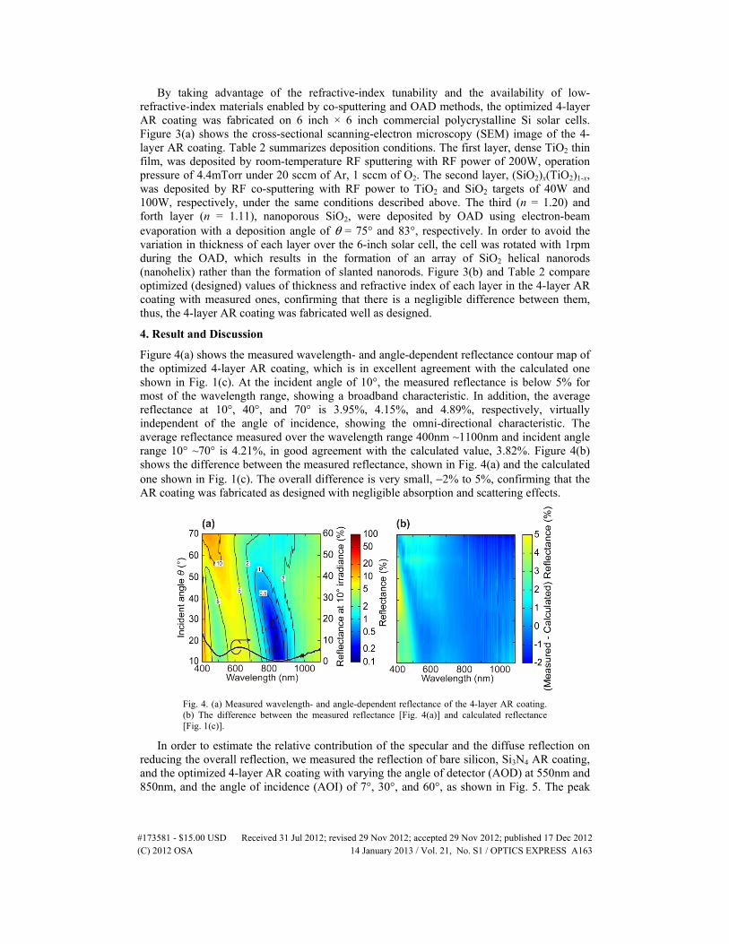
Figure 4(a) shows the measured wavelength- and angle-dependent reflectance contour map of the optimized 4-layer AR coating, which is in excellent agreement with the calculated one shown in Fig. 1(c). At the incident angle of 10°, the measured reflectance is below 5% for most of the wavelength range, showing a broadband characteristic. In addition, the average reflectance at 10°, 40°, and 70° is 3.95%, 4.15%, and 4.89%, respectively, virtually independent of the angle of incidence, showing the omni-directional characteristic. The average reflectance measured over the wavelength range 400nm ~1100nm and incident angle range 10° ~70° is 4.21%, in good agreement with the calculated value, 3.82%. Figure 4(b) shows the difference between the measured reflectance, shown in Fig. 4(a) and the calculated one shown in Fig. 1(c). The overall difference is very small, −2% to 5%, confirming that the AR coating was fabricated as designed with negligible absorption and scattering effects.
Fig. 4. (a) Measured wavelength- and angle-dependent reflectance of the 4-layer AR coating. (b) The difference between the measured reflectance [Fig. 4(a)] and calculated reflectance [Fig. 1(c)].
In order to estimate the relative contribution of the specular and the diffuse reflection on reducing the overall reflection, we measured the reflection of bare silicon, Si3N4 AR coating, and the optimized 4-layer AR coating with varying the angle of detector (AOD) at 550nm and 850nm, and the angle of incidence (AOI) of 7°, 30°, and 60°, as shown in Fig. 5. The peak
#173581 - $15.00 USD Received 31 Jul 2012; revised 29 Nov 2012; accepted 29 Nov 2012; published 17 Dec 2012(C) 2012 OSA 14 January 2013 / Vol. 21, No. S1 / OPTICS EXPRESS A163
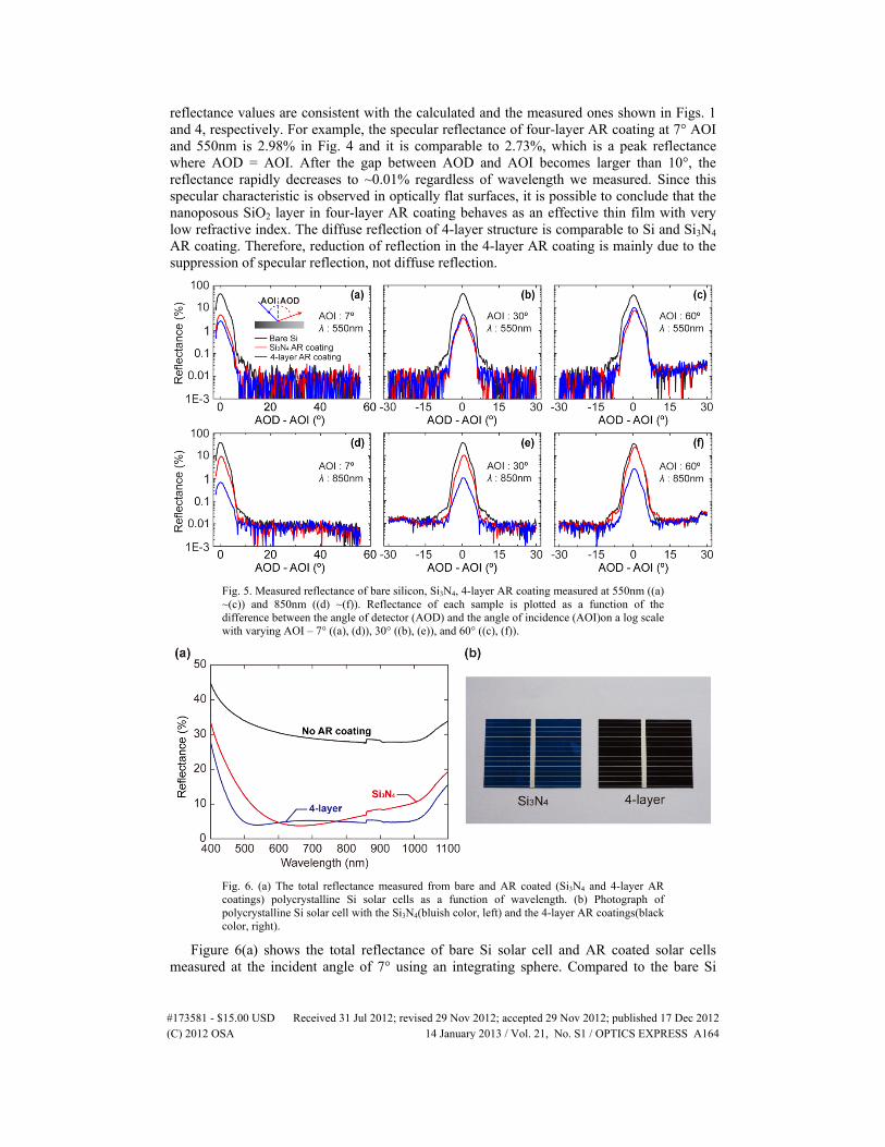
reflectance values are consistent with the calculated and the measured ones shown in Figs. 1 and 4, respectively. For example, the specular reflectance of four-layer AR coating at 7° AOI and 550nm is 2.98% in Fig. 4 and it is comparable to 2.73%, which is a peak reflectance where AOD = AOI. After the gap between AOD and AOI becomes larger than 10°, the reflectance rapidly decreases to ~0.01% regardless of wavelength we measured. Since this specular characteristic is observed in optically flat surfaces, it is possible to conclude that the nanoposous SiO2 layer in four-layer AR coating behaves as an effective thin film with very low refractive index. The diffuse reflection of 4-layer structure is comparable to Si and Si3N4 AR coating. Therefore, reduction of reflection in the 4-layer AR coating is mainly due to the suppression of specular reflection, not diffuse reflection.
Fig. 5. Measured reflectance of bare silicon, Si3N4, 4-layer AR coating measured at 550nm ((a) ~(c)) and 850nm ((d) ~(f)). Reflectance of each sample is plotted as a function of the difference between the angle of detector (AOD) and the angle of incidence (AOI)on a log scale with varying AOI – 7° ((a), (d)), 30° ((b), (e)), and 60° ((c), (f)).
Fig. 6. (a) The total reflectance measured from bare and AR coated (Si3N4 and 4-layer AR coatings) polycrystalline Si solar cells as a function of wavelength. (b) Photograph of polycrystalline Si solar cell with the Si3N4(bluish color, left) and the 4-layer AR coatings(black color, right).
Figure 6(a) shows the total reflectance of bare Si solar cell and AR coated solar cells measured at the incident angle of 7° using an integrating sphere. Compared to the bare Si
#173581 - $15.00 USD Received 31 Jul 2012; revised 29 Nov 2012; accepted 29 Nov 2012; published 17 Dec 2012(C) 2012 OSA 14 January 2013 / Vol. 21, No. S1 / OPTICS EXPRESS A164
solar cell, the solar cell coated with the Si3N4 and the 4-layer AR coating shows a significantly reduced total reflection. The reflectance of the Si3N4 AR coating has a minimum around 650nm and rapidly increases for other, especially shorter, wavelengths, whereas the reflectance of the optimized 4-layer AR coating shows a low reflectance over a wide range of wavelengths, confirming the broadband characteristic. Figure 6(b) shows pieces of the poly-silicon solar cells with a Si3N4 and the 4-layer AR coating. The solar cell with the Si3N4 AR coating looks bluish due to the high reflectance in the short-wavelength region. However, the solar cell with the 4-layer AR coating looks black due to the wide low reflection band covering most of the visible wavelength range. This broadband characteristic of the 4-layer AR coating is expected to cause high incident-photon-to-electron conversion efficiency (IPCE) values over wide range of wavelengths.
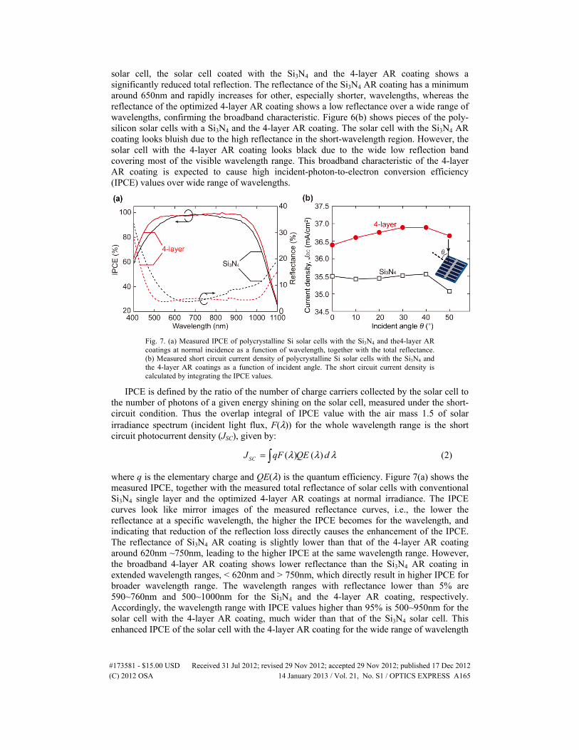
Fig. 7. (a) Measured IPCE of polycrystalline Si solar cells with the Si3N4 and the4-layer AR coatings at normal incidence as a function of wavelength, together with the total reflectance. (b) Measured short circuit current density of polycrystalline Si solar cells with the Si3N4 and the 4-layer AR coatings as a function of incident angle. The short circuit current density is calculated by integrating the IPCE values.
IPCE is defined by the ratio of the number of charge carriers collected by the solar cell to the number of photons of a given energy shining on the solar cell, measured under the short-circuit condition. Thus the overlap integral of IPCE value with the air mass 1.5 of solar irradiance spectrum (incident light flux, F(λ)) for the whole wavelength range is the short circuit photocurrent density (JSC), given by:
( ) ( )SCJ qF QE dλ λ λ= (2)
where q is the elementary charge and QE(λ) is the quantum efficiency. Figure 7(a) shows the measured IPCE, together with the measured total reflectance of solar cells with conventional Si3N4 single layer and the optimized 4-layer AR coatings at normal irradiance. The IPCE curves look like mirror images of the measured reflectance curves, i.e., the lower the reflectance at a specific wavelength, the higher the IPCE becomes for the wavelength, and indicating that reduction of the reflection loss directly causes the enhancement of the IPCE. The reflectance of Si3N4 AR coating is slightly lower than that of the 4-layer AR coating around 620nm ~750nm, leading to the higher IPCE at the same wavelength range. However, the broadband 4-layer AR coating shows lower reflectance than the Si3N4 AR coating in extended wavelength ranges, < 620nm and > 750nm, which directly result in higher IPCE for broader wavelength range. The wavelength ranges with reflectance lower than 5% are 590~760nm and 500~1000nm for the Si3N4 and the 4-layer AR coating, respectively. Accordingly, the wavelength range with IPCE values higher than 95% is 500~950nm for the solar cell with the 4-layer AR coating, much wider than that of the Si3N4 solar cell. This enhanced IPCE of the solar cell with the 4-layer AR coating for the wide range of wavelength
#173581 - $15.00 USD Received 31 Jul 2012; revised 29 Nov 2012; accepted 29 Nov 2012; published 17 Dec 2012(C) 2012 OSA 14 January 2013 / Vol. 21, No. S1 / OPTICS EXPRESS A165
is attributed to the reduced broadband reflection at the surface of the solar cell, leading to an increased transmission of incident photons with wide range of energies into the active region of the Si solar cell.
In order to investigate the angle-dependent reflection characteristic of AR coating, IPCE with varying incident angle from 0° to 50 o was measured. Figure 7(b) shows the short circuit current density, JSC, calculated from the measured IPCE using Eq. (2). Note that the exposed area by light source changes with incident angle, but the effect of enlarged area is not normalized. As expected from Fig. 7(a), the JSC of solar cell with the 4-layer AR coating is higher than that with the Si3N4 AR coating, not only for normal irradiance but also for the wide range of incident angle. We believe that this omni-directional characteristic of the 4-layer AR coating is very beneficial for harvesting more energy for a longer time during the day.
5. Conclusions
We have demonstrated an enhanced performance of polycrystalline Si solar cells by using nanostructured discrete 4-layer AR coatings with broadband and omni-directional characteristics. The GA-optimized 4-layer AR coating composed of nanohelix SiO2 arrays and co-sputtered (SiO2)x(TiO2)1-x thin film layers significantly outperforms the conventional Si3N4 AR coating over a wide range of wavelengths and angles of incidence, which directly causes a corresponding enhancement of IPCE of polycrystalline Si solar cells. The IPCE of the Si solar cell larger than 95% over a broad range of wavelengths, 500nm to 950nm, up to the incident angle of 50° is achieved. We attribute the performance enhancement of the discrete multilayer AR coatings to the interference effect optimized by the GA as well as a better refractive-index matching to the air enabled by nanohelix SiO2 arrays. Since the structure of discrete multilayer AR coatings can be optimized for application-specific requirements, thus they can be used for virtually any type of solar cells. Furthermore, optimized multilayer AR coatings can be readily implemented for various solar cells by conventional micro-electronics processes. Therefore, the optimized 4-layer AR coating, as an example of the potential multiple-discrete-layer tailored- and low-refractive index AR coating technology, is viable, readily applicable and highly promising for future generations of AR coating technology on various solar cell devices.
Acknowledgments
The authors gratefully acknowledge support by the 2011 Global Research Network program (2011-220-D00064) and Priority Research Centers Program through the National Research Foundation of Korea (NRF), and the Industrial Technology Development Program funded by Korean Ministry of Knowledge Economy (MKE), and Fusion Technology Center for Materials by POSCO.
#173581 - $15.00 USD Received 31 Jul 2012; revised 29 Nov 2012; accepted 29 Nov 2012; published 17 Dec 2012(C) 2012 OSA 14 January 2013 / Vol. 21, No. S1 / OPTICS EXPRESS A166