engineering technology 2°d
TRANSCRIPT
KHuLNA UNIVERSITY OF ENGINEERING & TECHNOLOGY B.Sc. Engineering 2°d Year 1st Term Examination, 2019
Department of Electronics and Communication Engineering ECE 2101
(Analog Electronics - II) TIME: 3 hours FULL MARKS: 210
N.B. i) Answer ANY THREE questions from each section in separate scripts. ii) Figures in the right margin indicate full marks.
SECTION A (Answer ANY THREE questions from this section in Script A)
1. a) Define tuned amplifier; Explain the tuned amplifier circuit with its applications. b) What are the characteristics of a parallel resonance circuit? Derive the expression for
resonance frequency of a parallel circuit. c) Graphically prove that bandwidth of a tuned circuit is proportional to the resistance
of inductor and selectivity is inversely proportional to the resistance of the inductor. d) · A parallel resonant circuit has a capacitance of 100 pF in one branch and inductance
of 100 µH plus a resistance of 100 in parallel branch. If the supply voltage is IOV, calculate (i) resonance frequency, (ii) impedance of the circuit and line current at resonance.
(08) (10)
(07)
(10)
..
2. a) Explain the operation of a double tuned amplifier. Why does the name of the · (10) amplifier is double tuned amplifier?
b) What is sinusoidal oscillator? List the requirements to work a transistor as an (08). oscillator.
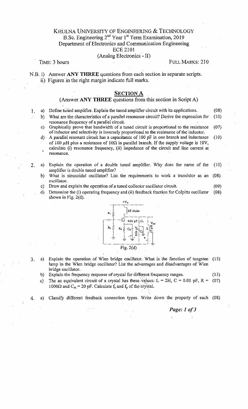
c) Draw and explain the operation of a tuned collector oscillator circuit. (09) d) Determine the (i) operating frequency and (ii) feedback fraction for Colpitts oscillator (08)
· shown in Fig. 2(d). +v ..
Fig. 2(d)
3. a) Explain the operation of Wien bridge oscillator. What is the function of tungsten (15) lamp in the Wien bridge oscillator? List the advantages and disadvantages of Wien bridge oscillator.
b) Explain the frequency response of crystal for different frequency ranges. (13) c) The ac equivalent circuit of a crystal has these'..v�.foes: L = 2H, C = 0.01 pF, R = (07)
1000.Q and Cm= 20 pF. Calculate fs and fp of thecrystal.:
4. a) Classify different feedback connection types. Write down the property .of each (08)
Page: 1 of3

feedback connection type. · �� ...... b) Derive the expression of output impedance of a current series feedback am;m,.�....._"
with necessary diagram, ', . c) Prove that the gain of an amplifier with negative feedback is more stable than the (1 O)·'·<, .
gain without feedback. d) An amplifier has an open-loop gain A = 100,000. A negative feedback of 10 dB is (08)
applied. Find (i) voltage gain with feedback and (ii) value of feedback fraction, f3.
·SECTIONB .,..._ (Answer ANY THREE questions from this section in Script B)
5. a) An ideal op-amp has (i) infinite input resistance, (ii) zero output resistance, (iii) (08) infinite common-mode rejection ratio, and (iv) infinite slew rate; write down the benefits of having these characteristics.
b) · Draw and explain (i) Equivalent circuit of an op-amp and (ii) Ideal voltage transfer (08) curve of an op-amp.
c) . "Negative feedback used in op-amp circuit is more practical for linear applications" - (07) justify the statement. Also, write down the applications of using positive feedback.
d) For the circuit shown in Fig. 5(d), assume ideal op-amp: (i) Identify the feedback (12) -topology, (ii) calculate 110, (iii) relate closed-loop gain with open-loop gain. v,
v . v, r-; ice r--�· <,
1 . v, r��:;·--·-- rl' t [vol\ ; Vo
v, r �'f .. . t .. Fig. 5(d)
6. a) Draw the block diagram of PLL and explain in brief. (08) b) Classify multivibrator. Explain the operation of bistable multivibrator with required (12)
circuit diagram. c) Write down the VCO operation of 555 timer with necessary block diagram. (07) d) In fig. 6(d), Vee= 12V, R = 33 KO, and C = 0.47 µF. (i) what is the minimum trigger (08)
voltage that produces an output pulse? (ii) what is t� maximum capacitor voltage? (iii) what is the width of the output pulse? ' ·
�--�---o+Voc
I .CJ. R� I I r i .!-l i, i I r-..---<-v ... •1f-l 1. sss I 1 lj i I I ;--1
c± � I i · 1 I to.o1.T i lT-�- .. 6 t' J:.
Trigger Fig. 6(d)
Page: 2 o/3

b) c)
d)
e)
8. a) b) c)
What is meant by order of filter? List the advantages of active filter over passive filter. Distinguish between common mode gain and differential gain of op-amp. How an op-amp circuit can be modified to act as an integrator? Deduce an expression of the output voltage for that modified circuit to validate that operation.
· How a comparator circuit can act as a voltage-level detector? Draw a + 1 OV voltage level detector with op-amp. Design a wide band-pass filter with {1, = 200Hz, fH = lKHz, and a passband gain= 4.
(06)
(04) (10)
(07)
(08)
Explain the operation of window detector and also write down it's applications. (09) Write short note on (i) Clipper, and (ii) Clamper. (06) Draw the output waveshape of the following clipper circuits. Assume diodes are ideal (10)
R=IKO vfC� v�" - Dt � � I ' O>-------�-�J ) -10V
(i)
VI - R . i +VIII C,----i'--./1/v- -=-- O + fl\."' v· D f v v0 W J-t-'_ T1
I '- . ; -Vm o-
(ii) Fig. 8(c) .
d) Draw the output waveshape of the following clamper circuits. Assume diodes are (10) " ideal.
c c - v;I 0-----1 ot l + Ju 0----1� * l o+ vb lOv 0-�=r R< Vo .L R"" Vo . I Yi . > -20vlT-+ v, 5V < -v ! L 1 T ) I
' 0 o- () 0- ; (i) (ii)
Fig. 8(d)
·.· ... ..
Page: 3 o/3


KHULNA UNIVERSITY OF ENGINEERING & TECHNOLOGY ·B.Sc. Engineering 2"dYear 1st Term Examination, 2019
Department of Electronics and Communication Engineering ECE 2103
(Digital Electronics and Logic Circuits) FULL MARKS: 210.
N.B. i) Answer ANY THREE questions from each section in separate scripts. ii) Figures in the right margin indicate full marks. ·
SECTION A (Answer ANY THREE questions from this section in Script A)
1. a) Represent the decimal number 8620 (i) in BCD, (ii) in.excess-J code, (iii) in 2,4,2,1 (08) code, and (iv) as a binary number. ·
. b) Perform the subtraction with the following binarynumbers using (i) 2's complement (10) and (ii) 1 's complement. Check the answer by straight subtraction. (100- 110000)2.
c) Express the following function in a sum of minterms and a product ofmaxterms. (09) · F(w,x,y,z) = yz + wxy' + wxz' + wxz -,
d) Define the following terms: (i) Duality princip]e (ii) Standard form (08)
2. a) Obtain the simplified expression in (i) Sum of products and (ii) Product of sums. (12) (A'+ B'+ DXA + B'-'+ c,(A'+_B + DJ(B + C'+ DJ
b) Simplify the following logic circuit as shown in figure 2(b). (12)
. Fig. 2(b) c) Show that a positive-logic AND gate is a negative-logic OR gate and vice-versa. (11)
TIME: 3 hours
3. ..
a) Design a combinational circuit that converts a decimal digit from the 2, 4, 2, 1 code to 8, 4, -2, -1 code. · -
b) Implement the four Boolean functions listed using three half-adder circuits. D = A(f)B$C ., E =ABC+ AB'C F = ABC'+ (A'+ B')C G = ABC
c) Implementa full-adder circuit with a decoder and two OR gates.
(12)
(12)
(11)
.. v', ...
4. a) Define multiplexer and demultiplexer. Implement the following function with a (10) multiplexer.
F (A,B,C,D) = .E(0,2,3,4,8, 10, 14) b) Show that the circuit in figure 4(b) behaves as an inverter with the following (13)
parameters: Re= 1 KO, Rs= 22 KO, Vee= 5V, hrc = 50, H = 5V (high level volatge), L = 0.2V (low level voltage).
+Vee
--Vo
Fig. 4(b)
Page: 1 o/2

c) Define Fan out and Noise margin characteristics of digital logic families and show (05) the circuit of three inputs NANI> gate using CMOS transistors .
. d) Explain the operation of common bus system using open collector gates. (07)
SECTIONB (Answer ANY THREE questions from this section in Script B)
5. a) What is sequential circuit? Draw the block diagram of a sequential circuit. (05) b) . Draw the diagram of RS, JK, D, and T flip-flop. Also write their characteristics table (12)
and excitation table. c) Show the operation of D-type edge-triggered flip-flop with necessary diagrams. (10) d) Draw the diagram of clocked master-slave JK flip-flop using NAND gates. (08)
6. · a) Write down the state table and draw the state diagram of the following sequential (12) circuit.
y
x , Ji Q2 B A
A' K2 Q2' B' x
Fig. 6{a)
Qi'---
B
x' B
b): Design a counter that counts the decimal digits according to Excess- 3 code using T (13) flip-flop.
c) Design a BCD counter with JK flip-flops. '· ..
(10)
7. · a) Design a serial adder using a sequential logic procedure. (10) b) The content of the shift register A and B is..,_1011 and 1101 as shown in figure 7(b). (12)
What will be the content of each register after 6..,clock pulses? Show the result for each clock pulse.
elk----�-----------.
Fig. 7(b) c) Show that in Dual slope AID converter, the output of the converter is proportional to (13)
the analog input voltage.
8. a) Define memory element. Show the information transfer process in a magnetic core memory during write operation.
b) Write short notes on EPROM and E2PROM. c) Construct a Johnson counter with 10 timing signals. d) Write down the differences between R-2R ladder and weighted register DIA
converter.
(10)
(08) (10) (07) ·
Page: 2 o/2

KHuLNA UNIVERSITY OF ENGINEERING & TECHNOLOGY B.Sc. Engineering 2°d Year 1st Term Examination, 2019
Department of Electronics and Communication Engineering ECE 2105
(Science of Materials)
TIME: 3 hours· FULL MAR.Ks: 210
N.B. i) Answer ANY THREE questions from each section in separate scripts. ii) Figures in the right margin indicate full marks.
SECTION A .
(Answer ANY THREE questions from this section in Script A)
1. a) Show that the atomic packing factor for face centered cube (fee) and hexagonal (14) close packed (hep) metals are the same.
b) What is meant by crystal imperfections? Classify them in the · order of their (07) geometry.
c) What is· 1attice parameter? Describe the BCC and HCP crystal structure with (09) relevant examples.
d) Consider the FCC unit cell of the Copper crystal: (i) How many atoms are there per (05) unit .cell? (ii) If 'R' is the radius of the Cu atom, show that the lattice parameter 'a'
is given by a = 2.JiR .
2. a) State the salient features of Einstein's model discussing the molar lattice specific (15) heat. Explain Einstein's equation for molar lattice specific heat both at lower temperatures and higher temperatures. Discuss its ag.�eement with the experimental data. ,·. .. -
(10)'
(10) b) Define phonon. What are the assumptions of Debye's theory? Show that at lower temperatures C, varies directly a:t T3.
'"-·�-
c) "The specific resistance of an electric .conductor is-directly proportional to the square root of the absolute temperature"-justify the statement.
. 3. a) Derive a relationship between electrical conductivity and thermal conductivity. (12) b) Discuss the breakdown of classical theory with special reference to mean free path (10)
of electrons and molar specific heat of metals. c) A beam of electrons; each of energy E, is incident on a rectangular potential barrier (13)
of width a and height Vo, where � > E .· Obtain an expression for the transmission · coefficient through the barrier.
, 4. a) Explain quantum mechanical tunneling in solids and its significance. (I 0) b) Briefly discuss different polarization mechanism in dielectrics. (12) c) Obtain Clausius-Mosotti equation for dielectrics and explain how it can be used to (13)
determine the dipole moment of a polar molecule.
Page: 1 o/2

SECTIONB .
(Answer ANY THREE questions from this section in Script B)
5. a) What is torque,? Show that magnetic moment is proportional to the orbital angular (08) momentum through a factor known as gyromagnetic moment.
.; b) What is magnetization vector? Explain how spin" magnetic- moment 'precess about (08) the magnetic field.
c) Write down Ampere's law. Prove that magnetostatic energy density, Evot = � HB, (lO)
where symbols have their usual meaning. d) Saturation magnetization Msat in iron is 1.75x106 Am·1. This corresponds to all (09)
possible net spins aligning parallel to each other. Calculate the effective number of Bohr magnetons per atom that would- give Msat, given that the density and relative atomic mass of iron are 7.86 cm"3 and 55.85, respectively.
6. a) Write short note about paramagnetism. Show that at room temperature, normalized, (07) saturated magnetization of iron is very close to 1.
b) Define magneto-crystalline anisotropy energy. Explain the optimization of domain (08) walL
c) Discuss the M versus H behavior of polycrystalline materials. (14) d) Consider a. toroidal coil with a silicon iron (Fe:2-4% Si). Suppose that the coil has
150 turns and is used in HF work with small signals. The mean diameter of the (06) toroid is 2.5 cm and the core diameter is 0.5 cm. If the core is (Fe: 2-4% Si), what is
. �· .. � . the approximate inductance of the coil?
7. a) Briefly explain Meissner effect. Why in an· engineering applications of (10) superconductor, type II materials are used?
b) What is wave front? Derive Cauchy short-form dispersion equation. (18) c) The relevant sellmier coefficients for diamond are A, = 0.1750 µm and Ai = 0.1060 (07)
. . . . um. Calculate its refractive index at 550 run (green light) to three decimal places.
8. a) Write down the significance of complex relative permittivity. (08) b) What is poynting vector? Prove that R + T= 1, where symbols have their usual ( 13)
meaning. c) "The colour of the sky appear to be blue in our eyes"-Explain the reason behind it. (06) d) Spectroscopic ellipsometry measurements on a silicon crystal at a wavelength of (08)
826.6 run shows that the real and imaginary parts of the complex relative permittivity are 13.488 and 0.038, respectively. Find the reflectance, transmittance, and resistivity. ·.
Page: 2 o/2

KHULNAUNIVERSITY OF ENGINEERING &TECHNOLOGY B.Sc. Engineeringz'" Year 1st Term Examination, 2019
Department of Electronics and Communication Engineering ECE-2107
(Signals and Systems)
TIME: 3 hours FULL MARKS: 210
N.B. i) Answer ANY THREE questions from each section in separate scripts. ii) Figures in the right margin indicate full marks.
SECTION A
(Answer ANY THREE questions from this section in Script A)
1. a) What are the major classifications of signals? Explain the operations performed on the independent variables in the processing of discrete signals.
b) � {cos(.7Z"n); n�O . Determine whether x( n) = . is energy or power signal and also find its
O; otherwise . corresponding energy or power.
c) Sketch the following signals: (i) x(t)=4r(3t-l), (ii) x(t)=7Z"(2t+5).
d) Determine whether the signal x(t) = sin Fzm + sin I Sm is periodic or not. Then find its fundamental period. Also, ·determine the even and odd components of the signal. ·
2. a). Define system. What are the properties of a system? b) The discrete-time system ·is represented by the following difference equation in which x(n)
is· input and y(n) is output: y(n)=3y(n-1)-n2x(n)+4x(n-1)""'"2x(n+l).Determine whether the system is (i) Time invariant (ii) Linear (iii) Causal .
c) Determine the impulse response for the systemh(n)for the system described by the. second order difference equation: y(n )+ 3y(n-1)+4y(n-2) =.�{n )+ ix(n-l). ·
· d) Check the BIBO stability of the following systems: y(n) = ax(n + 1) + bx(n- I).
(12)
(06)
(08)
(09)
(07) (12)
(08)
(08)
3. a) Find the output response of an FIR filter with impulse response h(n) = {1,2,�2,-l,O} and (12) input sequence x( n) == {l, 2, 3, 0} using linear convolution graphically.
b) What are the methods for representing a system? Draw the block diagram of the system (IO) . d2 · < . d d2
described by dt2 y(t) + 3 y(t) = dt x(t) + 2 dt2 x(t).
c) Find the complete solution of the first order recursive system of figure 3( c ), if the input is (13)
x(n) = (tr .u(n); initial condition, y(-1) = 8 and p =: .
x(n)
p s
Figure 3(c)
y(n)
Page: 1 o/3

4. a) Define state of a system. Find the state variable description of the RC circuit in figure 4(aj'-··if input is x(t) and output is currenty(t) through resistor R1. .
. y(t)
x(t)
R1 R2 C2 -
Figure 4(a). b) State and prove the Shannon-Nyquist sampling theorem. c) · What is meant by aliasing effect and what are the means to avoid it? d) Sketch the double-sided frequency spectrum of the signal
x(t) = lOcos( 2_0m-;). -oo < t < co ,
"
SECTIONB
(Answer ANY THREE questions from this section in Script B)
(] 0) (06) (05)'
5. a) Define Fourier transform pair. Derive Fourier transform pair .. of Gaussian pulse. (10) b) What is meant by Fourier series expansion? What are the "symmetry conditions" of Fourier (06)
series? c) What is signum function? Find the ·Fourier transform pair of this function. (09) d) Find the Fourier transform of the signal f(t) shown ·in frgure 5(d). (1 O)
f(t)
A
0 T
Figure 5(d)
6. _a) State and prove Persival'sIdentity for Fourier series. . (08) b) What is the main difference between Fourier transform and Laplace transform? Find the (08)
Laplace transform of t" function.
Page: 2 of 3.
(09)
Vo(s) 2
s
2/s
2
� ll(s) 1/s
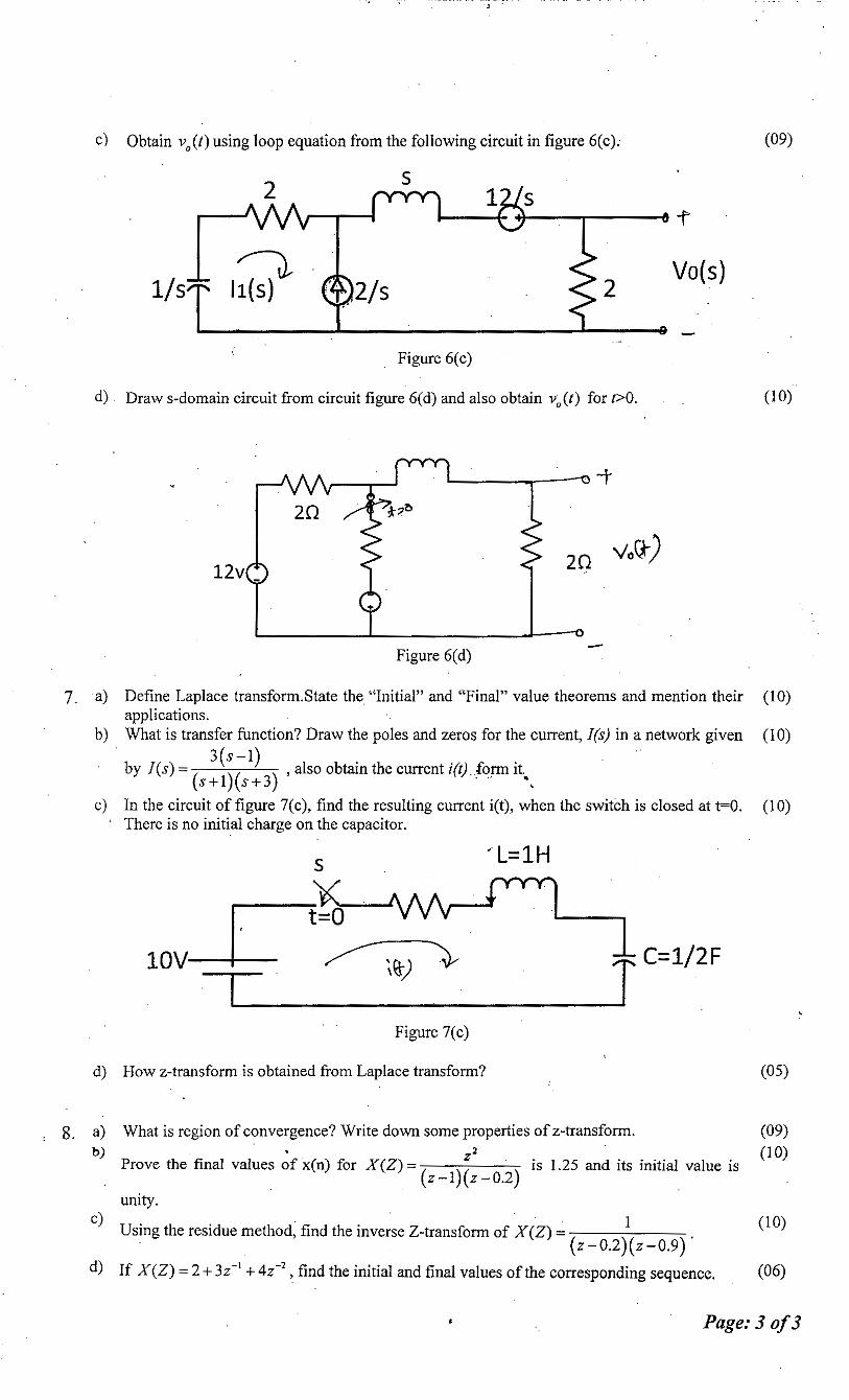
c) Obtain v0(1) using loop equation from the following circuit in figure 6(c).
Figure 6(c)
d). Draws-domain circuit from circuit figure 6(d) and also obtain v�(t) for t>O. (10)
12v
Figure 6(d)
20
-
vo\J-)
7. a) Define Laplace transform.State the. "Initial" and "Final" value theorems and mention their (10) applications.
b) What is transfer function? Draw the poles and zeros for the current, J(s) in a network given (10)
by I ( s) - (
3 () z1) ) , also obtain the currenti (t) form it s+l s+3 · ·· ",
c) In the circuit of figure 7( c ), find the resulting current i(t), when the switch is closed at t=O. (10) There is no initial charge on the capacitor.
s �L=lH
I t=O lOV----ij
__ l-- , =--� -- ;�) __ · T C=1/2F
Figure 7(c)
d) How z-transform is obtained from Laplace transform? (05)
(09) (10)
What is region of convergence? Write down some properties of z-transform. . • l
Prove the final values of x(n) for X(Z) = ( )( · ) is 1.25 and its initial value is z-1 z-0.2 . . .
unity.
c) Using the residue method; find the inverse Z-transform of X(Z) � 1 (IO) · . (z-0.2)(z-0.9) ·
d) If X(Z) = 2 + 3z-1 + 4z-2, find the initial and final values of the corresponding sequence. (06)
8. a) b)
Page: 3 o/3


KHULNA UNIVERSITY OF ENGINEERING & TECHNOLOGY B.Sc. Engineering 2nct Year 1st Term Examination, 2019
Department of Electronics and Communication Engineering Math 2109
(Mathematics-III)
· TIME: 3 hours FULL MARKS: 210
N.B. i) Answer A_NY THREE questions from each section in separate scripts. ii) Figures inthe right margin indicate full marks.
SECTION A.
(Answer ANY THREE questions from this 'section in Script A)
1. · a} Write the form of Fourier series for the functionf(x) with T=6 defined in the interval · (06) .. -2 < x < 4, along with the Fourier coefficients.
2.
· {x 0< x<2 b) . Find the amplitude of the third harmonic of f(x) = 2: 2 < x < 4
c) Find the Fourier series of the half wave rectified sinusoidal wave defined by
{sin t O < t < Jr i(t) =
0 ;r < t < 27f
i(t) = i(t + 2,r)
a) . f'(r) .. •· . d2f ·2 df Prove that V {/ (r)} = --r. Hence prove that V2 f f....r) = - 2 +- - . r dr r dr
b) Define solinoidal vector. Do the vector
A= x2yzT + (2yz-x + 4)7 + (y2 -z2 -xyz2)k solinoidal?
(17)
(12)
(12)
(09)
c) Show that
3.
representan electric field. Hence find the potential ¢( x,y,z), if ¢(2,3,-1) = 6.
a) Show that ii = ,: :, is unit normal to the surface ¢ ( x, y, z ). = c .
b) Pi
Show that if A= V¢ then JA.dris independent of the pathjoiningp1andp2.· P,
c) Evaluate fJXas, '»:here Sis the I 51 octant portion of the paraboloid y = 9-x2 -z2•
d) :
_ w l..erv. � -;::: 0;J + 1. )! + � l .j + ('t1 -71} J5. Evaluate JF.dr along the straight line joining A(2;-I,3) and B(3,4,l). ·
A .
(07)
(07)
(13)
(08)
w"',e,� E � 'cf"l + "a-i + d-r K - .
:·
Page: 1 o/3

. 4. · a) Use Green's theorem for the plane to evaluate
{ ( e'�nh-i ..- - xy) dx + ( log tan y + x2) dy J, where C consists of the lines. y=D, x+ 2y=4 c .
(10)
and x=O.
b) Evaluate {f1.nds where S is the entire surface of the region x=O, ;,=O, z=O, (15) s
x2 + y2 ·+ z2 = 16 and A= (x+ y)T +(y2 +xz )] +x�yz2k.
c) The acceleration a of a. rocket at any time t � 0 is given by (10)
a= e-1f ....... 6(t +l)}.+ 3 sintk '. If the velocity v and displacement r are zero at t=O,
then find v and r at any time.
SECTIONB
(Answer ANY THREE questions from this section in ScriptB)
5. a) When a system· of nonhomogeneous linear equations is said to be consistent? (10)
Calculate 'the currents in each wires of the following circuits:
30
60
� ', .. •·
+ 9V
Figure S(a) ·
,.' ' · · •· [2 3 4 c) Defi�e racl< of a matrix: Find the rank of A :: 4 6 '. 8
. · . 4 · 6 7 /o]. 10 .
Page: 2 of 3
(15)
. (10)
b) Apply rank test to solve the following system of linear equations:
2x1 + 3x2 + x3 = 9
X1 +2x2 +3x3 =6 3x1 + x2 + 2x3 = 8
Also, if consistent, then find its solutions.

6. a) Express A as the sum of a Harmitian and a skew Harmitian matrices, where
[2+i 3 4-i]
_ A= 2i 3+i 4 3 5 -7
(10)
b) . ·[2 -IJ Find the eigenvalues and the corresponding eigen vectors of A = 3 4 . _
c) Define symmetric and skew-symmetric matrices. Show that the diagonal elements of (12)
skew-symmetric matrices are zero.
(13)
7. a) Define Laplace transform. Find Laplace transform of
{ 0 0 s t < 1 if it F(t) = t-1 . t :2'.: 1 .
exists
(08)
b) Define periodic function with an example. Find L { F ( t)} of the following function ( 12)
given in figure 7(b).
F(t)
1
0 1 2 3 4 t Figure 7(b)
c) Find I (t) for the following circuit. Consider that initially there was no flow of current ( 15)
and the capacitor was uncharged. •· � ", .. ..
.lh .;
.lµF AC .10sin3t
50
Figure 7(c)
�
8. a) Write convolution theorem for inverse Laplace transform. Evaluate (12)
00Jcos6t-cos4t . -----,dt with the help of Laplace transform. O t
b) Evaluate r1{(-!s+2)e-2"}·
s -2s+6 . . . . f) C) · . . I \ I I � (13)
Define vector space. Can X1 =(2,3,-1) ,X2 =(f,-1,2), and X3 =(-1,1,3) .ftein a
Vector space?
Page: 3 of 3 .. t ------·-ft.
. (10)

.. �.