engineering materials (bme 15) - mmmut.ac.in
TRANSCRIPT

Engineering Materials (BME 15)
• In addition there are composites ,which are engineered combination oftwo or more different materials
• Apart from this classification we havedifferent types of materials in presentscenario, which are advance materials .(semiconductors, bio materials, smartmaterials and nanoengineeredmaterials)
Material science : it deals with thestudy of structure, properties andapplication of the materials so that theproperties of existing materials can bedeveloped, and new materials can bedeveloped to full fill our engineeringneeds.• solid materials have been
conveniently grouped into three basiccategories, ( based on chemical makeup and atomic structure)
• MATALS• CERAMICS• POLYMERS

Engineering materials
Metals polymersceramics
Ferrous
Non ferrous
Amorphous
Steels, cast iron, stainless steel etc.
Al, Cu, W, Ag etc.
Gels, glasses etc.
thermoplastics
thermosets
elastomers
Nylons, PVC, polyethylene etc.
Epoxies, phenolics, polymides etc.
Rubber, silicones etc.
Oxides, nitrides, carbides, glass ceramics, graphite , diamond
September 1, 2020 VIVEK CHAUDHARY 2

Atomic model
• During the latter part of the nineteenth century it was realized that many phenomena involving electrons in solids could not be explained in terms of classical mechanics.
• What followed was the establishment of a set of principles and laws that govern systems of atomic and subatomic entities that came to be known as quantum mechanics.
• An atomic model represents what the structure of an atom could look like , based on which we can predict its behavior.
• It is not necessarily a true picture of the exact structure of an atom.

Various scientists discovered the differentatomic models in progression of time and keepon moving towards more accurate atomic modelbut none of which is the perfect atomic modelto demonstrate the true picture inside the atom .
So let’s study some important atomic modelswhich are helpful to understand the concept ofthe structure of an atom.
4

1.Dalton’s model of the atom (1766-1844)
• Matters are made of very tiny particles called atoms which are indivisible structure.
• Atoms can neither be created nor destroyed.
• All atoms of particular elements are similar in all respects including identical mass , physical and chemical properties.
• Atoms of different elements shows different properties.
• Compound are formed when atoms of different elements combine in a fixed ratio.
• In this model electron and nucleus were unknown.
5
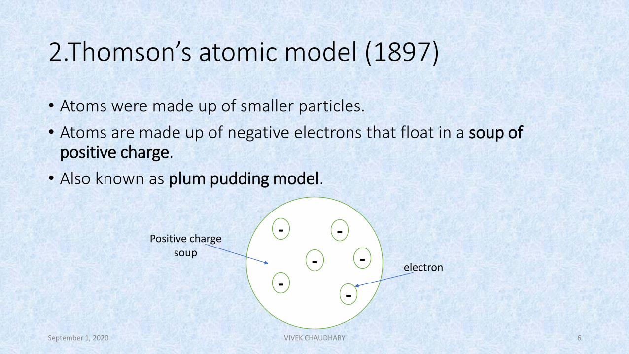
2.Thomson’s atomic model (1897)
• Atoms were made up of smaller particles.
• Atoms are made up of negative electrons that float in a soup of positive charge.
• Also known as plum pudding model.
--
---
-
Positive charge soup
electron
September 1, 2020 VIVEK CHAUDHARY 6

3.Rutherford’s atomic model (1911)• On the basis of alpha particles scattering experiment, Rutherford
described the atom as a dense tiny positively charged core callednucleus, in which nearly all mass is concentrated, around which thelightly weighted negative elements called electron propagate at somedistance similar to planets revolving around the sun.
• Also known as planetary model of the atom.
Reference: https://byjus.com/chemistry/rutherfords-model-of-atoms-and-its-limitations/September 1, 2020 VIVEK CHAUDHARY 7

4.Bohr’s model of the atom (1913)
• Bohr modified Rutherford’s atomic structure by describing that electrons have motion in fixed shells.
• Each shell has a certain energy level.
• It described electrons in atom in terms of both position (shell or orbit) and energy(quantized energy levels).
𝐸𝑛=−13.56 𝑧2
𝑛2eV 𝑅𝑛=
0.529 𝑛2
𝑧𝐴0
Where
𝐸𝑛= energy required for a electron to jump out of the n th orbit
𝑅𝑛=radius of n th orbitn= number of orbit Z= atomic number of elementSeptember 1, 2020 VIVEK CHAUDHARY 8

Bohr’s model of the atom (1913) continues….
Nucleus
Orbital electron
Orbit or shell
The first 3 electron energy states for the Bohr hydrogen atom.
n = shell or orbit number
September 1, 2020 VIVEK CHAUDHARY 9
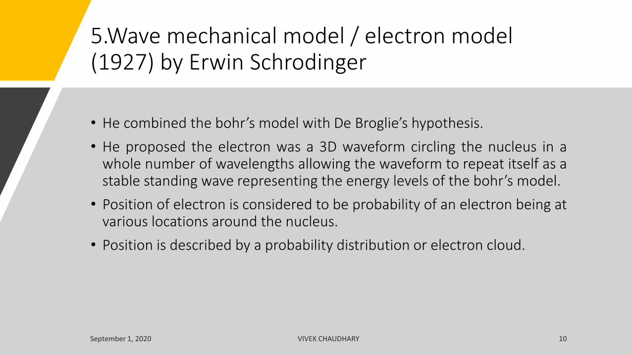
5.Wave mechanical model / electron model (1927) by Erwin Schrodinger
• He combined the bohr’s model with De Broglie’s hypothesis.
• He proposed the electron was a 3D waveform circling the nucleus in awhole number of wavelengths allowing the waveform to repeat itself as astable standing wave representing the energy levels of the bohr’s model.
• Position of electron is considered to be probability of an electron being atvarious locations around the nucleus.
• Position is described by a probability distribution or electron cloud.

Electron model (1927) continues…
• Using wave mechanics every electron in theatom is characterized by 4 parameters calledquantum number.
September 1, 2020 VIVEK CHAUDHARY 11

Crystal structures
• A crystalline material is one in which the atoms are situated in a repeating or periodic array over large atomic distances; that is, long-range order exists, such that upon solidification, the atoms will position themselves in a repetitive three-dimensional pattern, in which each atom is bonded to its nearest-neighbor atoms.
• Sometimes the term lattice is used in the context of crystal structures; in this sense lattice means a three-dimensional array of points coinciding with atom positions (or sphere centers). The point of center of atom in space lattice is known as lattice point.
• The properties of some materials are directly related to their crystal structures.
• significant property differences exist between crystalline and non crystalline materials having the same composition.
• All metals, many ceramic materials, and certain polymers form crystalline structures under normal solidification conditions.
September 1, 2020 VIVEK CHAUDHARY 12

Unit cell
• The atomic order in crystalline solids indicates that small groups of atoms form a repetitive pattern. Thus, in describing crystal structures, it is often convenient to subdivide the structure into small repeat entities called unit cells.
• Unit cells for most crystal structures are parallelepipeds or prisms having three sets of parallel faces.
• the unit cell is the basic structural unit or building block of the crystal structure and defines the crystal structure by virtue of its geometry and the atom positions within.
September 1, 2020 VIVEK CHAUDHARY 13

Coordination number and the atomic packing factor (APF).
• For metals, each atom has the same number of nearest-neighbor or touching atoms, which is the coordination number.
• The APF is the sum of the sphere volumes of all atoms within a unit cell (assuming the atomic hard-sphere model) divided by the unit cell volume.
APF=volume of atoms in a unit cell
total unit cell volume
September 1, 2020 VIVEK CHAUDHARY 14

Bravais lattice
• There are only 14 independent ways of arranging points in a three dimension space on pure symmetry consideration.
• If all the atoms at the lattice points are identical , the space lattice is said to be a bravais lattice.
• These 14 bravais lattices belong to 7 crystal systems.
September 1, 2020 VIVEK CHAUDHARY 15

September 1, 2020 VIVEK CHAUDHARY 16

September 1, 2020 VIVEK CHAUDHARY 17
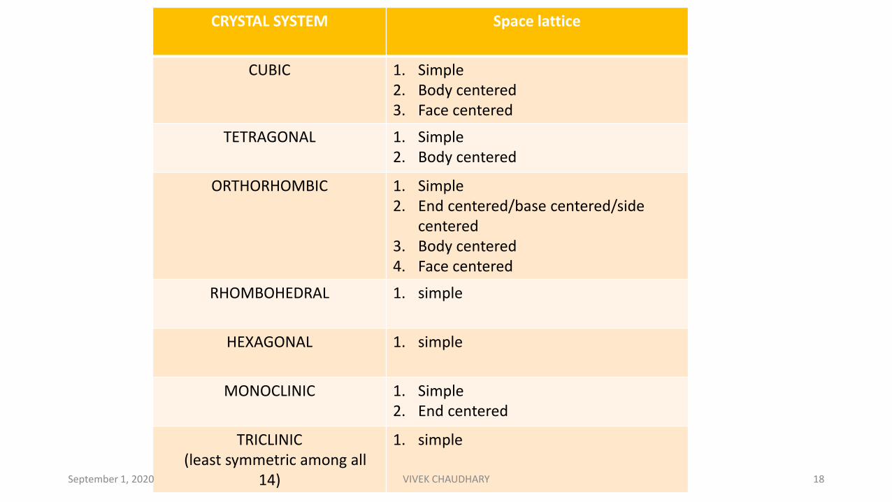
CRYSTAL SYSTEM Space lattice
CUBIC 1. Simple2. Body centered 3. Face centered
TETRAGONAL 1. Simple 2. Body centered
ORTHORHOMBIC 1. Simple2. End centered/base centered/side
centered3. Body centered4. Face centered
RHOMBOHEDRAL 1. simple
HEXAGONAL 1. simple
MONOCLINIC 1. Simple 2. End centered
TRICLINIC (least symmetric among all
14)
1. simple
September 1, 2020 VIVEK CHAUDHARY 18
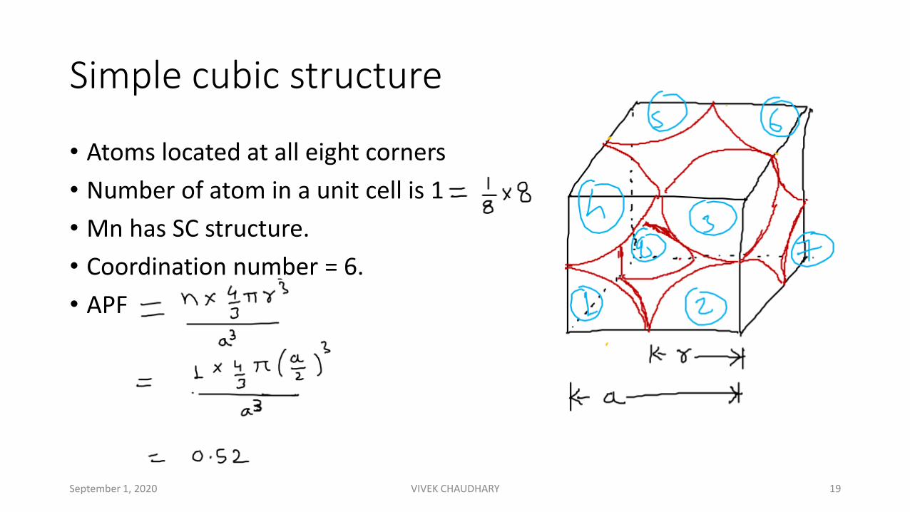
Simple cubic structure
• Atoms located at all eight corners.
• Number of atom in a unit cell is 1
• Mn has SC structure.
• Coordination number = 6.
• APF
September 1, 2020 VIVEK CHAUDHARY 19
Body centered cubic structure
• Atoms located at all eight corners and a single atom at the cube center.
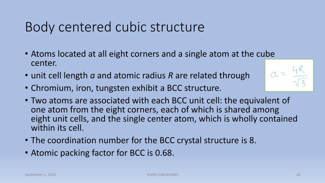
• unit cell length a and atomic radius R are related through
• Chromium, iron, tungsten exhibit a BCC structure.
• Two atoms are associated with each BCC unit cell: the equivalent of one atom from the eight corners, each of which is shared among eight unit cells, and the single center atom, which is wholly contained within its cell.
• The coordination number for the BCC crystal structure is 8.
• Atomic packing factor for BCC is 0.68.
September 1, 2020 VIVEK CHAUDHARY 20

September 1, 2020 VIVEK CHAUDHARY 21
Face centered cubic structure (FCC)
• The crystal structure found for many metals has a unit cell of cubic geometry, with atoms located at each of the corners and the centers of all the cube faces.
• Some of the familiar metals having this crystal structure are copper, aluminum, silver, and gold.
• Coordination number = 12
• Number of atoms within unit cell = 4
September 1, 2020 VIVEK CHAUDHARY 22
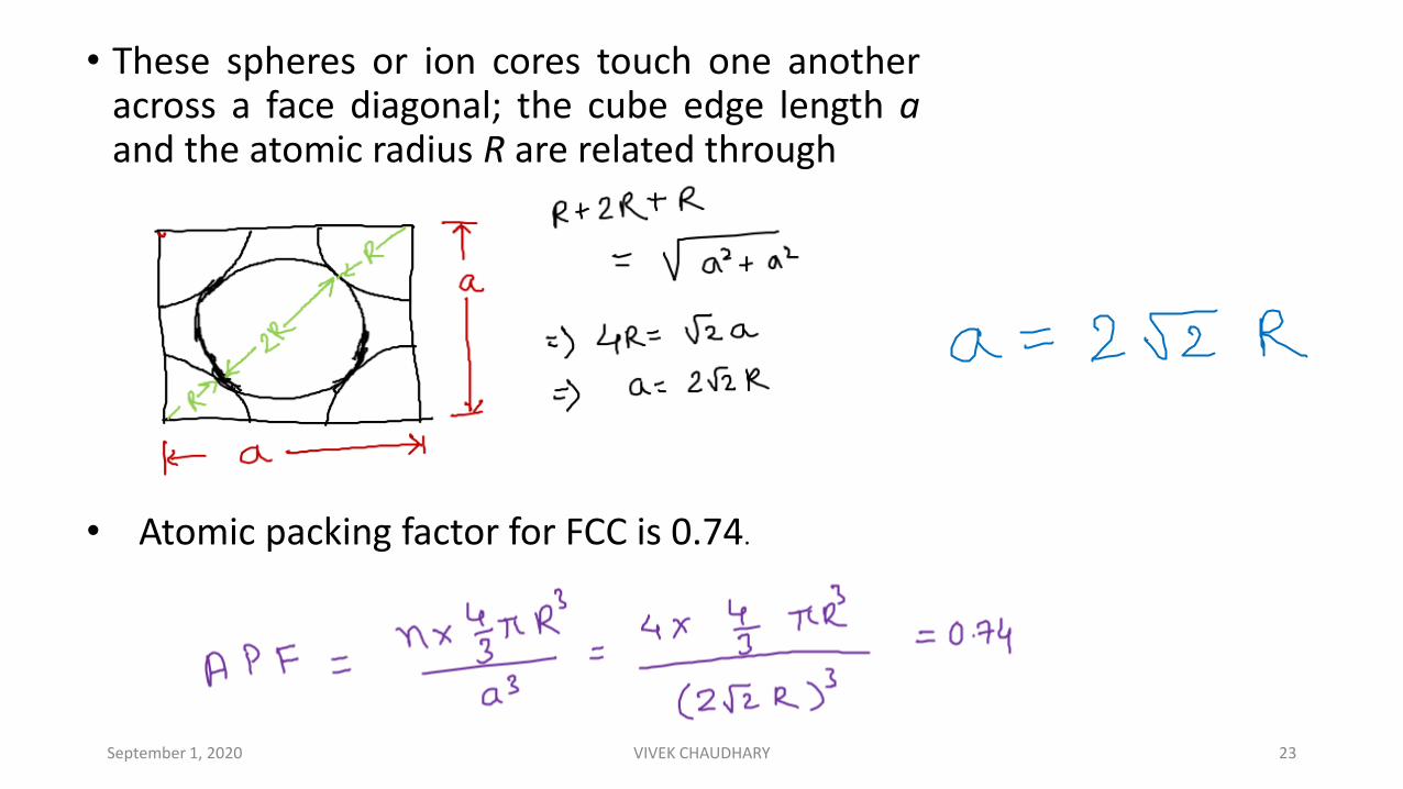
• These spheres or ion cores touch one anotheracross a face diagonal; the cube edge length aand the atomic radius R are related through
• Atomic packing factor for FCC is 0.74.
September 1, 2020 VIVEK CHAUDHARY 23

Hexagonal Close-Packed Crystal Structure (HCP)• The top and bottom faces of the unit cell consist of six atoms that
form regular hexagons and surround a single atom in the center.Another plane that provides three additional atoms to the unit cell issituated between the top and bottom planes.
• The coordination number and the atomic packing factor for the HCP crystal structure are the same as for FCC: 12 and 0.74, respectively.
• Total number of atoms within the unit cell is 6.
September 1, 2020 VIVEK CHAUDHARY 24

September 1, 2020 VIVEK CHAUDHARY 25

2
3 4
7
1
8 109
c
6
a
5
b
Consider atom ‘a’ that touches 6 atoms in the planeshown. We can see the arrangement of atoms in thisplane. similar planes are also present over andbelow the plane shown. So think how can atomsarrange themselves to accommodate properly.
In similar way another three atoms touches atom ‘a’
So total 12 atoms touches atom ‘a’ . It is true for
any atom in the structure. That is coordinator number
September 1, 2020 VIVEK CHAUDHARY 26

2
3 4
7
1
8 109
c
6
a
5
b
• Hexagonal consists of 3 layers of atoms (see 1st fig) and suppose the layer shown here is the top layer of hexagonal.(in middle layer, 3 atoms present that are within the hexagonal and not shared with other. )
• Consider 3 hexagonal which has centered atom named 4, b and 8.
• ‘a’ is common in these 3 hexagonal and above this layer there is another layer (hexagonal) ,where ‘a’ is shared by 3 hexagonal.
• So the corner atom is shared by 6 hexagonal.• Center atom (b) is shared by 2 hexagonal . That is above the
plane shown.
September 1, 2020 VIVEK CHAUDHARY 27

Crystallographic Points, Directions, and Planes
• When dealing with crystalline materials, it often becomes necessary to specify a particular pointwithin a unit cell, a crystallographic direction, or some crystallographic plane of atoms.
• Labeling conventions have been established in which three numbers or indices are used to designatepoint locations, directions, and planes.
• The basis for determining index values is the unit cell, with a right-handed coordinate systemconsisting of three (x, y, and z) axes situated at one of the corners and coinciding with the unit celledges, as shown in Figure .
• For some crystal systems—namely, hexagonal, rhombohedral, monoclinic, and triclinic—the threeaxes are not mutually perpendicular, as in the familiar Cartesian coordinate scheme.
A unit cell with x, y, and z coordinate axes, showing axial lengths (a,
b, and c) and interaxial angles(α, β , and γ ).
September 1, 2020 VIVEK CHAUDHARY 28

LINEAR AND PLANAR DENSITIES• Directional equivalency is related to linear density in the sense that, for a particular
material, equivalent directions have identical linear densities. The corresponding parameter for crystallographic planes is planar density, and planes having the same planar density values are also equivalent.
• Linear density (LD) is defined as the number of atoms per unit length whose centers lieon the direction vector for a specific crystallographic direction; (1 diameter= 1 atom)
• 𝐿𝐷 =𝑁𝑢𝑚𝑏𝑒𝑟 𝑜𝑓 𝑎𝑡𝑜𝑚𝑠 𝑐𝑒𝑛𝑡𝑒𝑟𝑒𝑑 𝑜𝑛 𝑑𝑖𝑟𝑒𝑐𝑡𝑖𝑜𝑛 𝑣𝑒𝑐𝑡𝑜𝑟
𝑙𝑒𝑛𝑔𝑡ℎ 𝑜𝑓 𝑑𝑖𝑟𝑒𝑐𝑡𝑖𝑜𝑛 𝑣𝑒𝑐𝑡𝑜𝑟
September 1, 2020 VIVEK CHAUDHARY 29
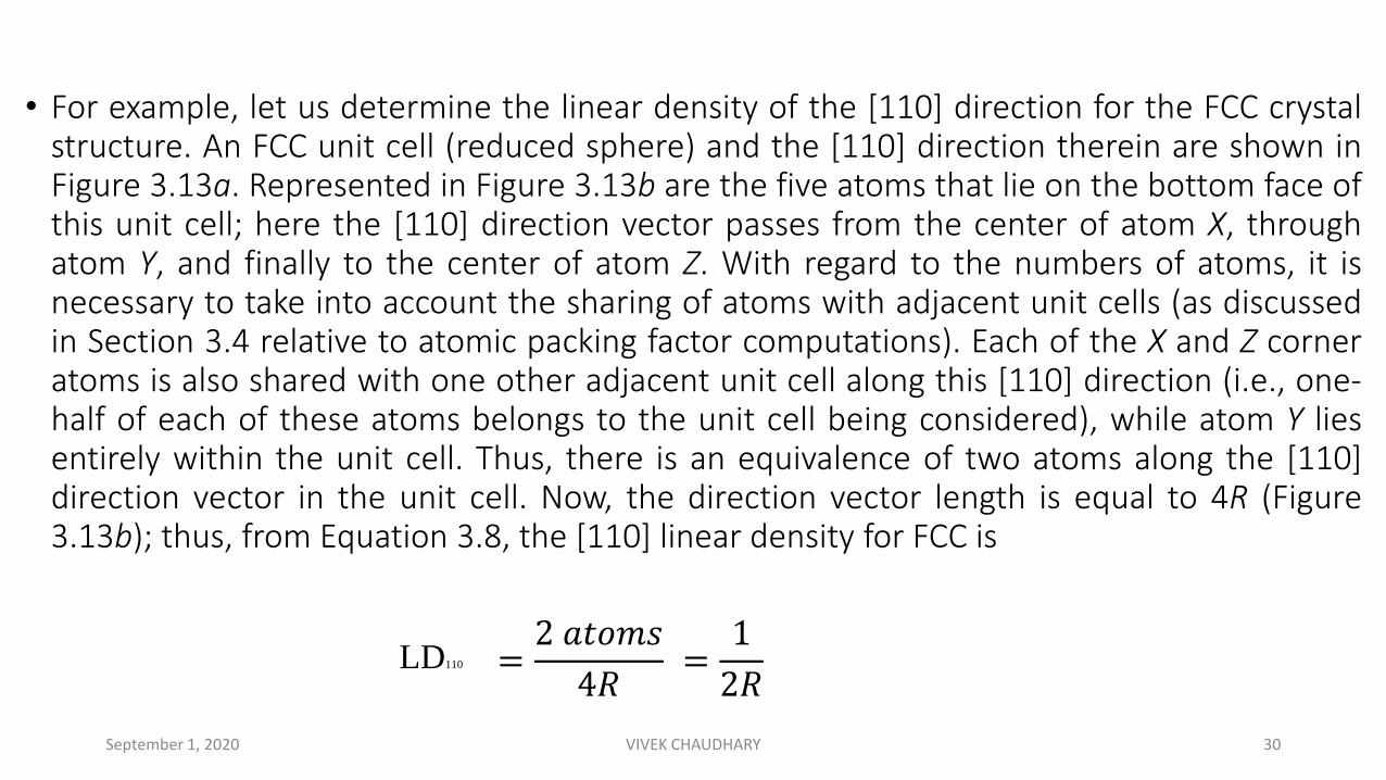
• For example, let us determine the linear density of the [110] direction for the FCC crystalstructure. An FCC unit cell (reduced sphere) and the [110] direction therein are shown inFigure 3.13a. Represented in Figure 3.13b are the five atoms that lie on the bottom face ofthis unit cell; here the [110] direction vector passes from the center of atom X, throughatom Y, and finally to the center of atom Z. With regard to the numbers of atoms, it isnecessary to take into account the sharing of atoms with adjacent unit cells (as discussedin Section 3.4 relative to atomic packing factor computations). Each of the X and Z corneratoms is also shared with one other adjacent unit cell along this [110] direction (i.e., one-half of each of these atoms belongs to the unit cell being considered), while atom Y liesentirely within the unit cell. Thus, there is an equivalence of two atoms along the [110]direction vector in the unit cell. Now, the direction vector length is equal to 4R (Figure3.13b); thus, from Equation 3.8, the [110] linear density for FCC is
LD110 =2 𝑎𝑡𝑜𝑚𝑠
4𝑅=
1
2𝑅
September 1, 2020 VIVEK CHAUDHARY 30
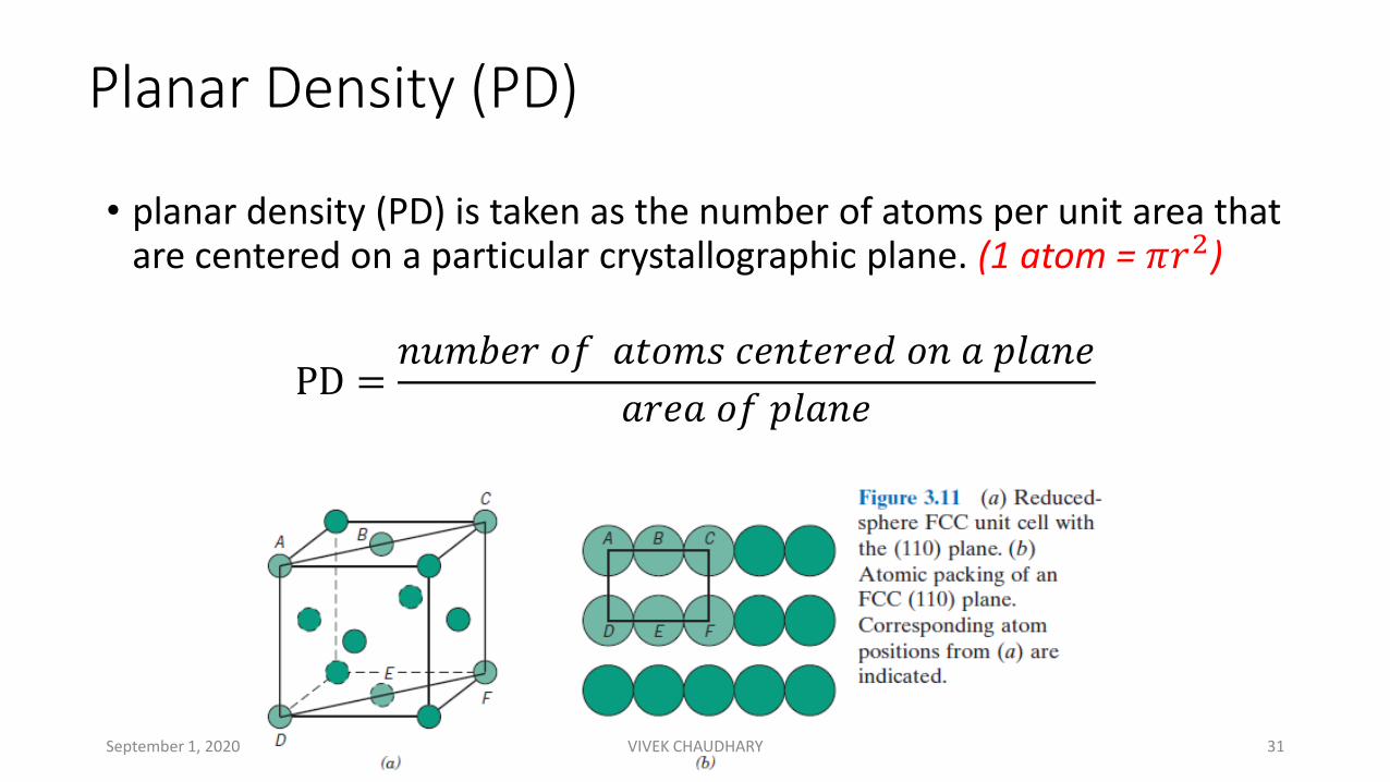
Planar Density (PD)
• planar density (PD) is taken as the number of atoms per unit area that are centered on a particular crystallographic plane. (1 atom = 𝜋𝑟2)
PD =𝑛𝑢𝑚𝑏𝑒𝑟 𝑜𝑓 𝑎𝑡𝑜𝑚𝑠 𝑐𝑒𝑛𝑡𝑒𝑟𝑒𝑑 𝑜𝑛 𝑎 𝑝𝑙𝑎𝑛𝑒
𝑎𝑟𝑒𝑎 𝑜𝑓 𝑝𝑙𝑎𝑛𝑒
September 1, 2020 VIVEK CHAUDHARY 31
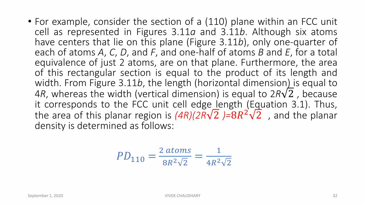
• For example, consider the section of a (110) plane within an FCC unitcell as represented in Figures 3.11a and 3.11b. Although six atomshave centers that lie on this plane (Figure 3.11b), only one-quarter ofeach of atoms A, C, D, and F, and one-half of atoms B and E, for a totalequivalence of just 2 atoms, are on that plane. Furthermore, the areaof this rectangular section is equal to the product of its length andwidth. From Figure 3.11b, the length (horizontal dimension) is equal to4R, whereas the width (vertical dimension) is equal to 2R 2 , becauseit corresponds to the FCC unit cell edge length (Equation 3.1). Thus,the area of this planar region is (4R)(2R 2 )=8𝑅2 2 , and the planardensity is determined as follows:
𝑃𝐷110 =2 𝑎𝑡𝑜𝑚𝑠
8𝑅2 2=
1
4𝑅2 2
September 1, 2020 VIVEK CHAUDHARY 32

POINT COORDINATES• The position of any point located within a unit cell may be
specified in terms of its coordinates as fractional multiplesof the unit cell edge lengths (i.e., in terms of a, b, and c).
• To illustrate, consider the unit cell and the point P situatedtherein as shown in Figure
• We specify the position of P in terms of the generalizedcoordinates q, r, and s where q is some fractional length of aalong the x axis, r is some fractional length of b along the yaxis, and similarly for s. Thus, the position of P is designatedusing coordinates q r s with values that are less than orequal to unity.
• Furthermore, we have chosen not to separate thesecoordinates by commas or any other punctuation marks(which is the normal convention).
September 1, 2020 VIVEK CHAUDHARY 33
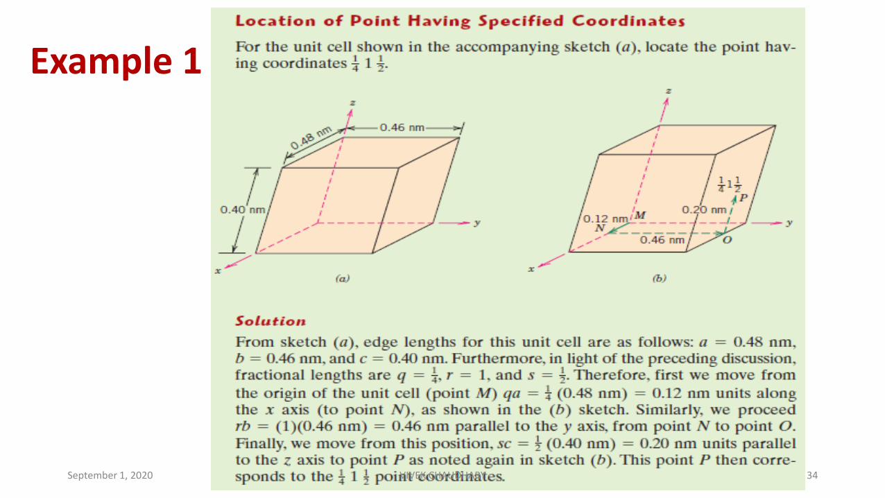
Example 1
September 1, 2020 VIVEK CHAUDHARY 34
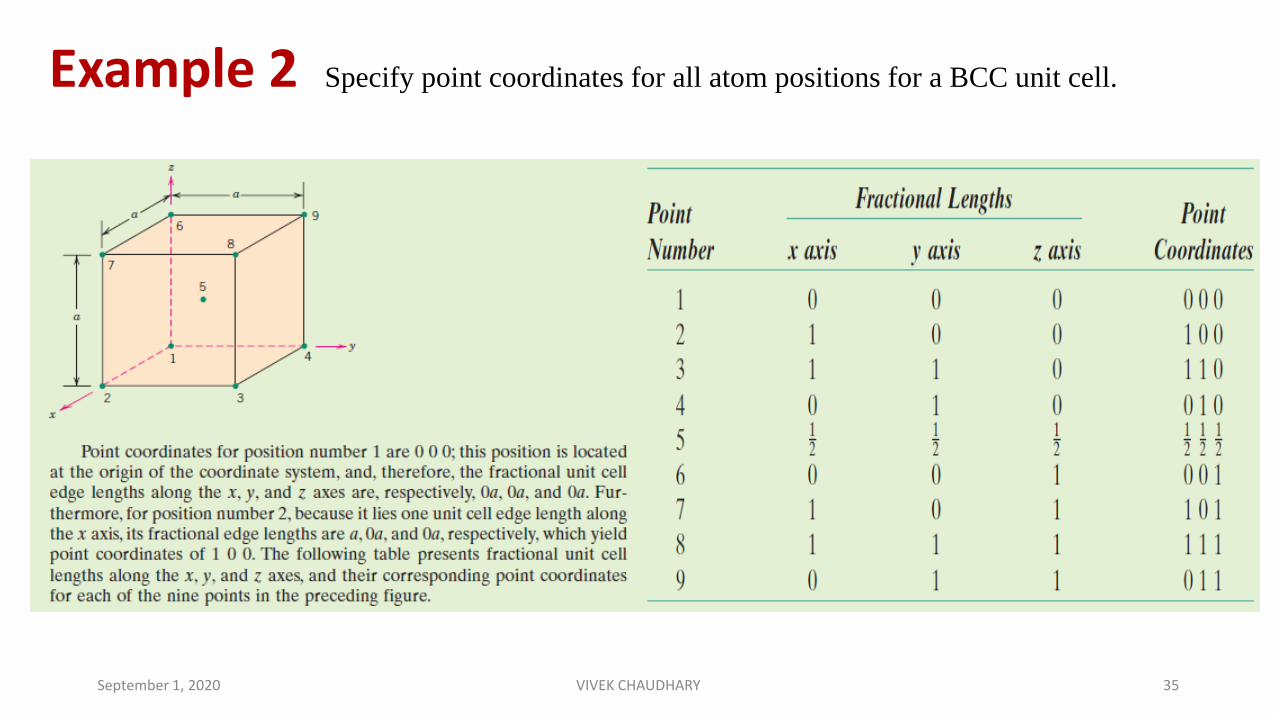
Example 2 Specify point coordinates for all atom positions for a BCC unit cell.
September 1, 2020 VIVEK CHAUDHARY 35

CRYSTALLOGRAPHIC DIRECTIONS
A crystallographic direction is defined as a line between two points, or a vector. The following steps areused to determine the three directional indices:
1. A vector of convenient length is positioned such that it passes through the origin of the coordinatesystem. Any vector may be translated throughout the crystal lattice without alteration, if parallelismis maintained.
2. The length of the vector projection on each of the three axes is determined; these are measured interms of the unit cell dimensions a, b, and c.
3. These three numbers are multiplied or divided by a common factor to reduce them to the smallestinteger values.
4. The three indices, not separated by commas, are enclosed in square brackets, thus: [uvw]. The u, v,and w integers correspond to the reduced projections along the x, y, and z axes, respectively.
For each of the three axes, there will exist both positive and negative coordinates. Thusnegative indices are also possible, which are represented by a bar over the appropriateindex.
September 1, 2020 VIVEK CHAUDHARY 36
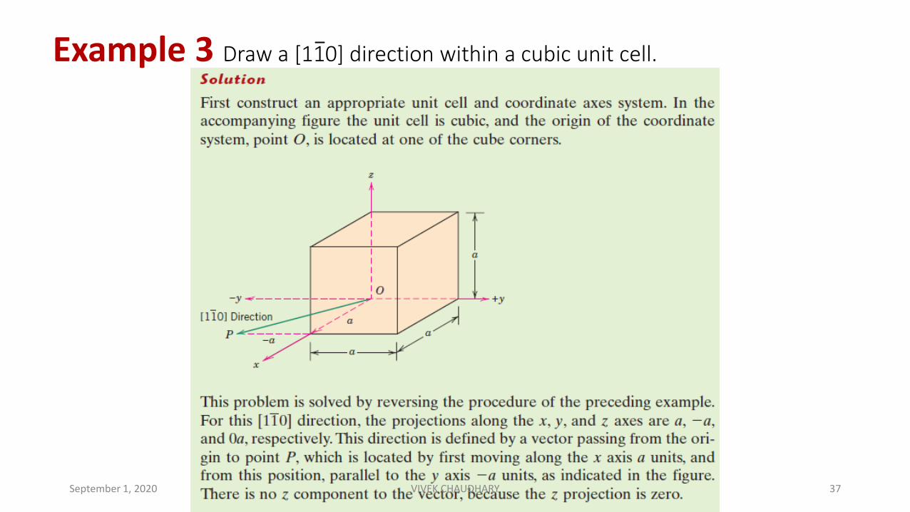
Example 3 Draw a [110] direction within a cubic unit cell.
September 1, 2020 VIVEK CHAUDHARY 37

Family of crystallographic direction
• For some crystal structures, several nonparallel directions with differentindices are crystallographically equivalent; this means that the spacing ofatoms along each direction is the same. (having same linear density)
• For example, in cubic crystals, all the directions represented by the followingindices are equivalent: [100], [ 100], [010], [010], [001], and [001].
• As a convenience, equivalent directions are grouped together into a family,which are enclosed in angle brackets, thus: <100>.
• Furthermore, directions in cubic crystals having the same indices withoutregard to order or sign—for example, [123] and [213] are equivalent.
• This is, in general, not true for other crystal systems. For example, for crystalsof tetragonal symmetry, [100] and [010] directions are equivalent, whereas[100] and [001] are not.
September 1, 2020 VIVEK CHAUDHARY 38
CRYSTALLOGRAPHIC PLANEScrystallographic planes are specified by three Miller indices as (hkl). Any two planes parallel to eachother are equivalent and have identical indices. The procedure used to determine the h, k, and l indexnumbers is as follows:
1. If the plane passes through the selected origin, either another parallel plane must be constructedwithin the unit cell by an appropriate translation, or a new origin must be established at thecorner of another unit cell.
2. At this point the crystallographic plane either intersects or parallels each of the three axes; thelength of the planar intercept for each axis is determined in terms of the lattice parameters a, b,and c.
3. The reciprocals of these numbers are taken. A plane that parallels an axis may be considered tohave an infinite intercept, and, therefore, a zero index.
4. If necessary, these three numbers are changed to the set of smallest integers by multiplication or division by a common factor.
5. Finally, the integer indices, not separated by commas, are enclosed within parentheses, thus: (hkl).
An intercept on the negative side of the origin is indicated by a bar or minus sign positioned over the appropriate index. Furthermore, reversing the directions of all indices specifies another plane parallel to, on the opposite side of, and equidistant from the origin.
September 1, 2020 VIVEK CHAUDHARY 39

Example 3
• Determine the Miller indices for the plane shown in the accompanying sketch (a).
September 1, 2020 VIVEK CHAUDHARY 40

September 1, 2020 VIVEK CHAUDHARY 41
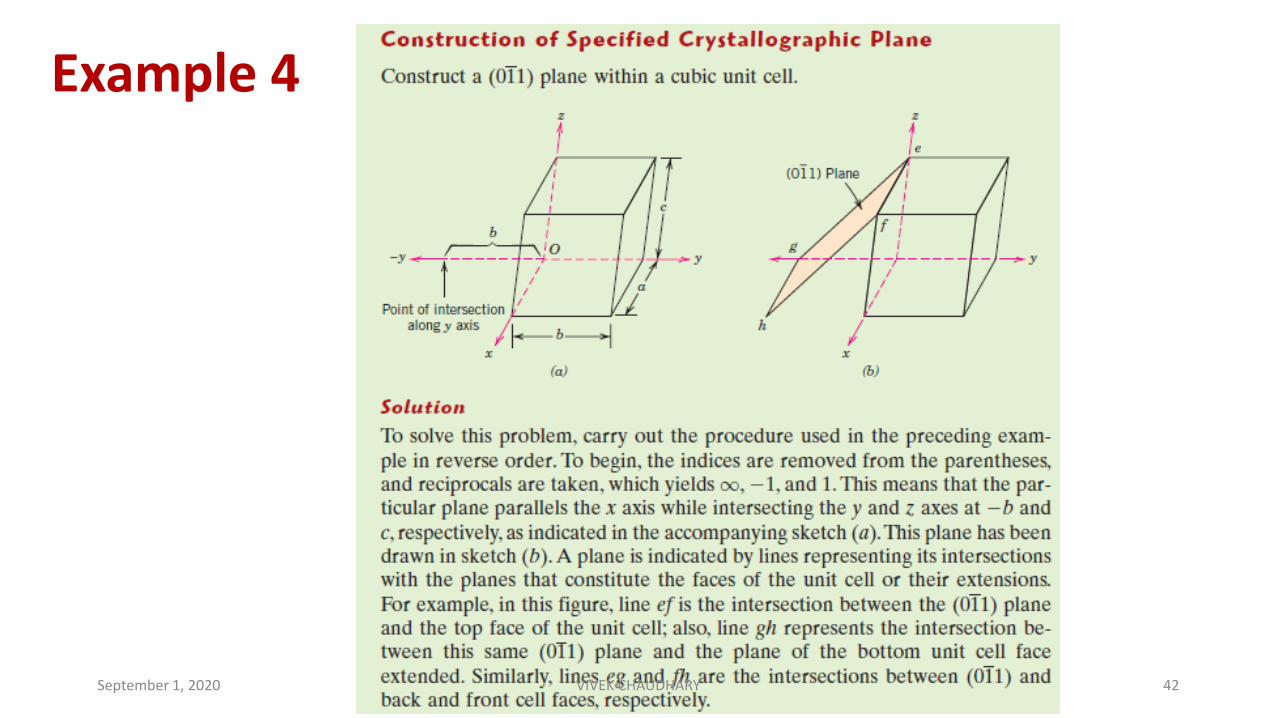
Example 4
September 1, 2020 VIVEK CHAUDHARY 42

Reference: http://www.examhill.com/miller-indices/
Some planes are shown in a cubic unit cell
September 1, 2020 VIVEK CHAUDHARY 43

Imperfection in solid
• Any crystal with perfectly regular crystal structure is called ideal crystal while realcrystals always have certain defects or imperfections.
• Many of the properties of materials are profoundly sensitive to deviations fromcrystalline perfection; the influence is not always adverse, and often specificcharacteristics are deliberately fashioned by the introduction of controlledamounts or numbers of particular defects.
• Crystalline defect refers to a lattice irregularity having one or more of itsdimensions on the order of an atomic diameter.
September 1, 2020 VIVEK CHAUDHARY 44

S No. Imperfection type Size of defect Sub type
1 Point defects Zero dimensional defect(interatomic space)
1. Vacancy2. Substitutional impurity3. Interstitial impurityFrenkel’s defectSchottky’s defect
2 Line defect One dimensional defect 1. Edge dislocation2. Screw dislocation3. Mixed dislocation
3 Surface imperfection(interfacial defect)
Two dimensional defect 1. External surface2. Grain boundary3. Twinning4. Low angle boundary5. High angle boundary6. Twist boundary7. Stacking fault
4 Volume defect Three dimensional defect 1. pores2. Foreign particle inclusion3. Non compatibility region4. Dissimilar natured regions
September 1, 2020 VIVEK CHAUDHARY 45

Vacancy defect
• In crystallography , a vacancy is a point defect in a crystalwhere a atom is missing from one of the lattice site.
• Vacancy defects are lattice sites which would be occupiedin a perfect crystal, but are vacant. If a neighboring atommoves to occupy the vacant site, the vacancy moves in theopposite direction to the site which used to be occupied bythe moving atom.
• The stability of the surrounding crystal structure guaranteesthat the neighboring atoms will not simply collapse aroundthe vacancy. In some materials, neighboring atoms actuallymove away from a vacancy, because they experienceattraction from atoms in the surroundings. A vacancy (orpair of vacancies in an ionic solid) is sometimes calleda Schottky defect.
September 1, 2020 VIVEK CHAUDHARY 46
Interstitial defect
• Interstitial defect are atoms that occupy a site in the crystal structure atwhich there is usually not an atom.
• They are generally high energy configurations. Small atoms (mostlyimpurities) in some crystals can occupy interstices without high energy,such as hydrogen in palladium.
• The interstitial atom has more chances to be lodge with in a crystalstructure has low atomic packing factor.
• It produces atomic distortion.
• A nearby pair of a vacancy and an interstitial is often called a Frenkeldefect or Frenkel pair. This is caused when an ion moves into an interstitialsite and creates a vacancy.
September 1, 2020 VIVEK CHAUDHARY 47
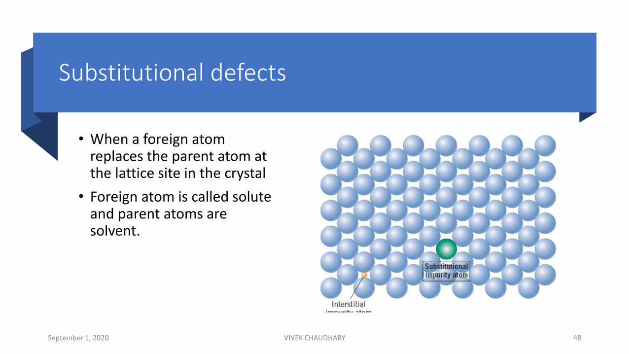
Substitutional defects
• When a foreign atom replaces the parent atom at the lattice site in the crystal
• Foreign atom is called solute and parent atoms are solvent.
September 1, 2020 VIVEK CHAUDHARY 48

Reference: https://www.majordifferences.com/2013/02/difference-between-schottky-defect-and.html#.Xxhc8FUzbIU
September 1, 2020 VIVEK CHAUDHARY 49
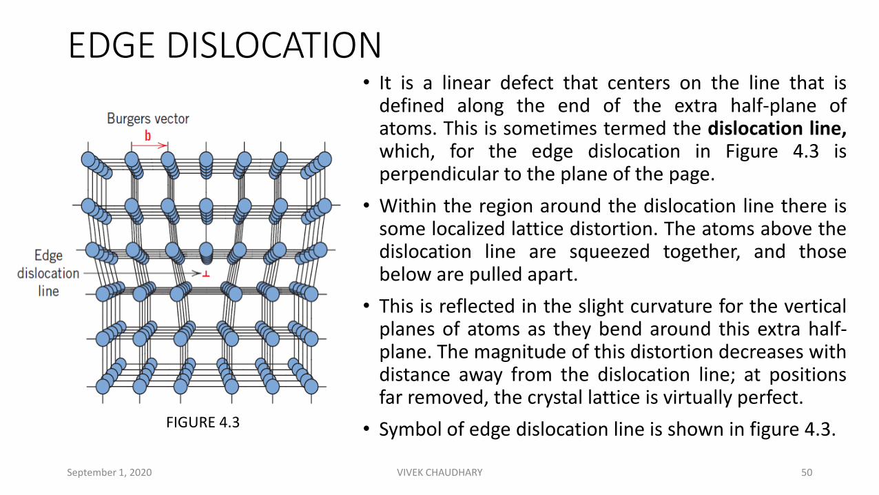
EDGE DISLOCATION• It is a linear defect that centers on the line that is
defined along the end of the extra half-plane ofatoms. This is sometimes termed the dislocation line,which, for the edge dislocation in Figure 4.3 isperpendicular to the plane of the page.
• Within the region around the dislocation line there issome localized lattice distortion. The atoms above thedislocation line are squeezed together, and thosebelow are pulled apart.
• This is reflected in the slight curvature for the verticalplanes of atoms as they bend around this extra half-plane. The magnitude of this distortion decreases withdistance away from the dislocation line; at positionsfar removed, the crystal lattice is virtually perfect.
• Symbol of edge dislocation line is shown in figure 4.3.
September 1, 2020 VIVEK CHAUDHARY 50
FIGURE 4.3

SCREW DISLOCATION
September 1, 2020 VIVEK CHAUDHARY 51

• Another type of dislocation, called a screw dislocation, may bethought of as being formed by a shear stress that is applied toproduce the distortion shown in Figure 4.4a: the upper front regionof the crystal is shifted one atomic distance to the right relative tothe bottom portion. The atomic distortion associated with a screwdislocation is also linear and along a dislocation line, line AB in Figure4.4b.
• The screw dislocation derives its name from the spiral or helical pathor ramp that is traced around the dislocation line by the atomicplanes of atoms. Sometimes the symbol is used to designate ascrew dislocation.
September 1, 2020 VIVEK CHAUDHARY 52

MIXED DISLOCATION
September 1, 2020 VIVEK CHAUDHARY 53
MIXED DISLOCATION
• Most dislocations found in crystalline materials are probably neither pure edge nor pure screw, but exhibit components of both types; these are termed mixed dislocations.
• All three dislocation types are represented schematically in Figure 4.5; the lattice distortion that is produced away from the two faces is mixed, having varying degrees of screw and edge character.
The magnitude and direction of the lattice distortion associated with a
dislocation is expressed in terms of a Burgers vector, denoted by a b. Burgers vectors are indicated in Figures 4.3 and 4.4 for edge and screw dislocations, respectively.
September 1, 2020 VIVEK CHAUDHARY 54

INTERFACIAL DEFECTS
• Interfacial defects are boundaries that have two dimensions and normallyseparate regions of the materials that have different crystal structures and/orcrystallographic orientations. These imperfections include external surfaces,grain boundaries, phase boundaries, twin boundaries, and stacking faults.
September 1, 2020 VIVEK CHAUDHARY 55

External Surfaces
• One of the most obvious boundaries is the external surface, along which the crystal structure terminates.
• Surface atoms are not bonded to the maximum number of nearest neighbors, and are therefore in a higher energy state than the atoms at interior positions.
• To reduce this energy, materials tend to minimize, if at all possible, the total surface area. For example, liquids assume a shape having a minimum area—the droplets become spherical.
VIVEK CHAUDHARY September 1, 2020 56
Grain Boundaries
• Another interfacial defect, the grain boundary is the boundary separating two small grains or crystals having different crystallographic orientations in polycrystalline materials.
• When this orientation mismatch is slight, on the order of a few degrees, then the term small- (or low-) angle grain boundary is used. (figure 4.7 in next slide)
• One simple small-angle grain boundary is formed when edge dislocations are aligned in the manner of Figure 4.8(in next slide). This type is called a tilt boundary; the angle of misorientation, is also indicated in the figure.
• There is an interfacial or grain boundary energy like the surface energy.
• The magnitude of this energy is a function of the degree of misorientation, being larger for high-angle boundaries.
• Grain boundaries are more chemically reactive than the grains themselves as a consequence of this boundary energy.
• Impurity atoms often preferentially segregate along these boundaries because of their higher energy state
September 1, 2020 VIVEK CHAUDHARY 57

September 1, 2020 VIVEK CHAUDHARY 58
Figure 4.7 Figure 4.8

Twin Boundaries
• A twin boundary is a special type of grainboundary across which there is a specific mirrorlattice symmetry; that is, atoms on one side ofthe boundary are located in mirror-imagepositions of the atoms on the other side.
September 1, 2020 VIVEK CHAUDHARY 59
• Twins result from atomic displacements that are produced from appliedmechanical shear forces (mechanical twins), and also during annealing heattreatments following deformation (annealing twins).
• Annealing twins are typically found in metals that have the FCC crystalstructure, whereas mechanical twins are observed in BCC and HCP metals.

Thank you
September 1, 2020 VIVEK CHAUDHARY 60