engineering lab ii ece 1201 electronics lab...
TRANSCRIPT
- 1 -
ENGINEERING LAB II ECE 1201
ELECTRONICS LAB MANUAL
SEMESTER _________ YEARS _____________
NAME:
MATRIC NO:
- 2 -
INDEX Page 3 – DRESS CODES AND ETHICS.
Page 4 – SAFETY.
Page 8 – INTRODUCTION TO ENGINEERING LAB II
( ECE 1201 ).
Page 14 – EXPERIMENT 1
–DIODE CHARACTERISTICS.
Page 17 – EXPERIMENT 2
–ZENER DIODE CHARACTERISTICS.
Page 20 – EXPERIMENT 3
–WAVE RECTIFIER AND CLIPPER CIRCUITS.
Page 29 – EXPERIMENT 4
–BJT CHARACTERISTICS & COMMON-EMITTER
TRANSISTOR AMPLIFIER.
Page 33– EXPERIMENT 5
–BJT BIASING CIRCUITS.
Page 40 – EXPERIMENT 6
–JFET CHARACTERISTICS & COMMON SOURCE
AMPLIFIER.
Page 47 – EXPERIMENT 7
–FET BIASING CIRCUITS.
Page 56 –EXPERIMENT 8
– INVERTING AND NON-INVERTING OP AMP
Page 60–EXPERIMENT 9
– SUMMING,SUBTRACTING,INTERGRATOR AND DIFFERENTIATING OP
AMPS.

- 3 -
DRESS CODES AND ETHICS
24:31 And say to the believing women that they should lower their gaze and guard their modesty; that they should not display their beauty and ornaments
except what (must ordinarily) appear thereof; that they should draw their veils over their bosoms and not display their beauty except to their husbands, their fathers, their husband's fathers, their sons, their husbands' sons, their brothers or
their brothers' sons, or their sisters' sons, or their women, or the slaves whom their right hands possess, or male servants free of physical needs, or small
children who have no sense of the shame of sex; and that they should not strike their feet in order to draw attention to their hidden ornaments. And O ye Believers! turn ye all together towards Allah, that ye may attain Bliss.
Katakanlah kepada wanita yang beriman: ”Hendaklah mereka menahan
pandangannya, dan memelihara kemaluannya, dan janganlah mereka menampakkan perhiasannya, kecuali yang (biasa) nampak daripadanya. Dan
hendaklah mereka menutup kain kudung ke dadanya, dan janganlah menampakkan perhiasannya, kecuali kepada suami mereka, atau ayah mereka, atau ayah suami mereka, atau putera-putera mereka, atau putera-putera suami
mereka, atau saudara-saudara laki-laki mereka, atau putera-putera saudara laki-laki mereka, atau putera-putera saudara perempuan mereka, atau wanita–wanita
Islam, atau budak-budak yang mereka miliki, atau pelayan-pelayan laki-laki yang tidak mempunyai keinginan (terhadap wanita) atau anak-anak yang belum mengerti tentang aurat wanita. Dan janganlah mereka memukulkan kakinya agar
diketahui perhiasan yang mereka sembunyikan. Dan bertaubatlah kamu sekelian kepada Allah, hai orang-orang yang beriman supaya beruntung. (An-Nuur 31)
- 4 -
SAFETY
Safety in the electrical laboratory, as everywhere else, is a matter of the knowledge of potential
hazards, following safety precautions, and common sense. Observing safety precautions is
important due to pronounced hazards in any electrical/computer engineering laboratory. Death
is usually certain when 0.1 ampere or more flows through the head or upper thorax and have
been fatal to persons with coronary conditions. The current depends on body resistance, the
resistance between body and ground, and the voltage source. If the skin is wet, the heart is
weak, the body contact with ground is large and direct, then 40 volts could be fatal. Therefore,
never take a chance on "low" voltage. When working in a laboratory, injuries such as burns,
broken bones, sprains, or damage to eyes are possible and precautions must be taken to avoid
these as well as the much less common fatal electrical shock. Make sure that you have handy
emergency phone numbers to call for assistance if necessary. If any safety questions arise,
consult the lab demonstrator or technical assistant/technician for guidance and instructions.
Observing proper safety precautions is important when working in the laboratory to prevent
harm to yourself or others. The most common hazard is the electric shock which can be fatal if
one is not careful.
Acquaint yourself with the location of the following safety items within the lab.
a. fire extinguisher
b. first aid kit
c. telephone and emergency numbers
ECE Department 03-6196 4530
Kulliyyah of Engineering Deputy
Dean’s Student Affairs 03-6196 4410
IIUM Security 03-6196 5555
IIUM Clinic 03-6196 4444
Electric shock
Shock is caused by passing an electric current through the human body. The severity depends
mainly on the amount of current and is less function of the applied voltage. The threshold of
electric shock is about 1 mA which usually gives an unpleasant tingling. For currents above 10
mA, severe muscle pain occurs and the victim can't let go of the conductor due to muscle
spasm. Current between 100 mA and 200 mA (50 Hz AC) causes ventricular fibrillation of the
heart and is most likely to be lethal.
- 5 -
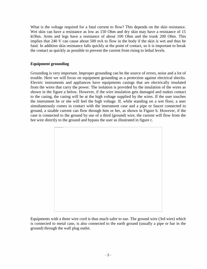
What is the voltage required for a fatal current to flow? This depends on the skin resistance.
Wet skin can have a resistance as low as 150 Ohm and dry skin may have a resistance of 15
kOhm. Arms and legs have a resistance of about 100 Ohm and the trunk 200 Ohm. This
implies that 240 V can cause about 500 mA to flow in the body if the skin is wet and thus be
fatal. In addition skin resistance falls quickly at the point of contact, so it is important to break
the contact as quickly as possible to prevent the current from rising to lethal levels.
Equipment grounding
Grounding is very important. Improper grounding can be the source of errors, noise and a lot of
trouble. Here we will focus on equipment grounding as a protection against electrical shocks.
Electric instruments and appliances have equipments casings that are electrically insulated
from the wires that carry the power. The isolation is provided by the insulation of the wires as
shown in the figure a below. However, if the wire insulation gets damaged and makes contact
to the casing, the casing will be at the high voltage supplied by the wires. If the user touches
the instrument he or she will feel the high voltage. If, while standing on a wet floor, a user
simultaneously comes in contact with the instrument case and a pipe or faucet connected to
ground, a sizable current can flow through him or her, as shown in Figure b. However, if the
case is connected to the ground by use of a third (ground) wire, the current will flow from the
hot wire directly to the ground and bypass the user as illustrated in figure c.
Equipments with a three wire cord is thus much safer to use. The ground wire (3rd wire) which
is connected to metal case, is also connected to the earth ground (usually a pipe or bar in the
ground) through the wall plug outlet.
- 6 -
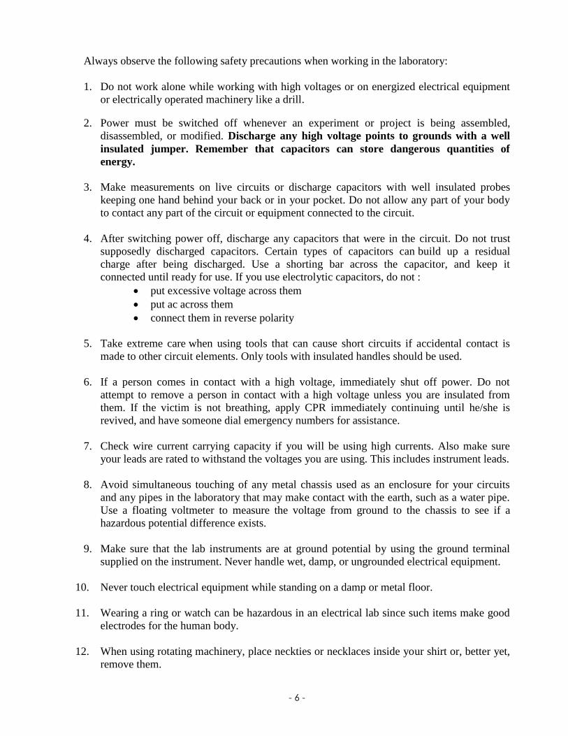
Always observe the following safety precautions when working in the laboratory:
1. Do not work alone while working with high voltages or on energized electrical equipment
or electrically operated machinery like a drill.
2. Power must be switched off whenever an experiment or project is being assembled,
disassembled, or modified. Discharge any high voltage points to grounds with a well
insulated jumper. Remember that capacitors can store dangerous quantities of
energy.
3. Make measurements on live circuits or discharge capacitors with well insulated probes
keeping one hand behind your back or in your pocket. Do not allow any part of your body
to contact any part of the circuit or equipment connected to the circuit.
4. After switching power off, discharge any capacitors that were in the circuit. Do not trust
supposedly discharged capacitors. Certain types of capacitors can build up a residual
charge after being discharged. Use a shorting bar across the capacitor, and keep it
connected until ready for use. If you use electrolytic capacitors, do not :
put excessive voltage across them
put ac across them
connect them in reverse polarity
5. Take extreme care when using tools that can cause short circuits if accidental contact is
made to other circuit elements. Only tools with insulated handles should be used.
6. If a person comes in contact with a high voltage, immediately shut off power. Do not
attempt to remove a person in contact with a high voltage unless you are insulated from
them. If the victim is not breathing, apply CPR immediately continuing until he/she is
revived, and have someone dial emergency numbers for assistance.
7. Check wire current carrying capacity if you will be using high currents. Also make sure
your leads are rated to withstand the voltages you are using. This includes instrument leads.
8. Avoid simultaneous touching of any metal chassis used as an enclosure for your circuits
and any pipes in the laboratory that may make contact with the earth, such as a water pipe.
Use a floating voltmeter to measure the voltage from ground to the chassis to see if a
hazardous potential difference exists.
9. Make sure that the lab instruments are at ground potential by using the ground terminal
supplied on the instrument. Never handle wet, damp, or ungrounded electrical equipment.
10. Never touch electrical equipment while standing on a damp or metal floor.
11. Wearing a ring or watch can be hazardous in an electrical lab since such items make good
electrodes for the human body.
12. When using rotating machinery, place neckties or necklaces inside your shirt or, better yet,
remove them.
- 7 -
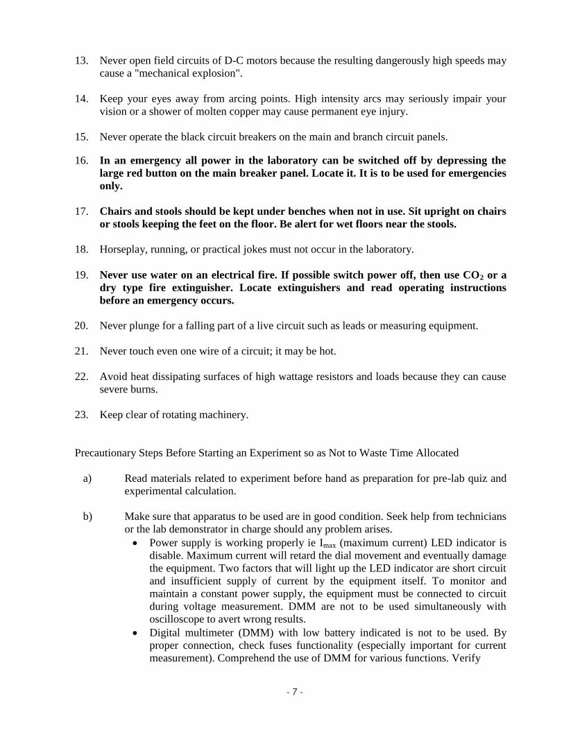
13. Never open field circuits of D-C motors because the resulting dangerously high speeds may
cause a "mechanical explosion".
14. Keep your eyes away from arcing points. High intensity arcs may seriously impair your
vision or a shower of molten copper may cause permanent eye injury.
15. Never operate the black circuit breakers on the main and branch circuit panels.
16. In an emergency all power in the laboratory can be switched off by depressing the
large red button on the main breaker panel. Locate it. It is to be used for emergencies
only.
17. Chairs and stools should be kept under benches when not in use. Sit upright on chairs
or stools keeping the feet on the floor. Be alert for wet floors near the stools.
18. Horseplay, running, or practical jokes must not occur in the laboratory.
19. Never use water on an electrical fire. If possible switch power off, then use CO2 or a
dry type fire extinguisher. Locate extinguishers and read operating instructions
before an emergency occurs.
20. Never plunge for a falling part of a live circuit such as leads or measuring equipment.
21. Never touch even one wire of a circuit; it may be hot.
22. Avoid heat dissipating surfaces of high wattage resistors and loads because they can cause
severe burns.
23. Keep clear of rotating machinery.
Precautionary Steps Before Starting an Experiment so as Not to Waste Time Allocated
a) Read materials related to experiment before hand as preparation for pre-lab quiz and
experimental calculation.
b) Make sure that apparatus to be used are in good condition. Seek help from technicians
or the lab demonstrator in charge should any problem arises.
Power supply is working properly ie Imax (maximum current) LED indicator is
disable. Maximum current will retard the dial movement and eventually damage
the equipment. Two factors that will light up the LED indicator are short circuit
and insufficient supply of current by the equipment itself. To monitor and
maintain a constant power supply, the equipment must be connected to circuit
during voltage measurement. DMM are not to be used simultaneously with
oscilloscope to avert wrong results.
Digital multimeter (DMM) with low battery indicated is not to be used. By
proper connection, check fuses functionality (especially important for current
measurement). Comprehend the use of DMM for various functions. Verify
- 8 -
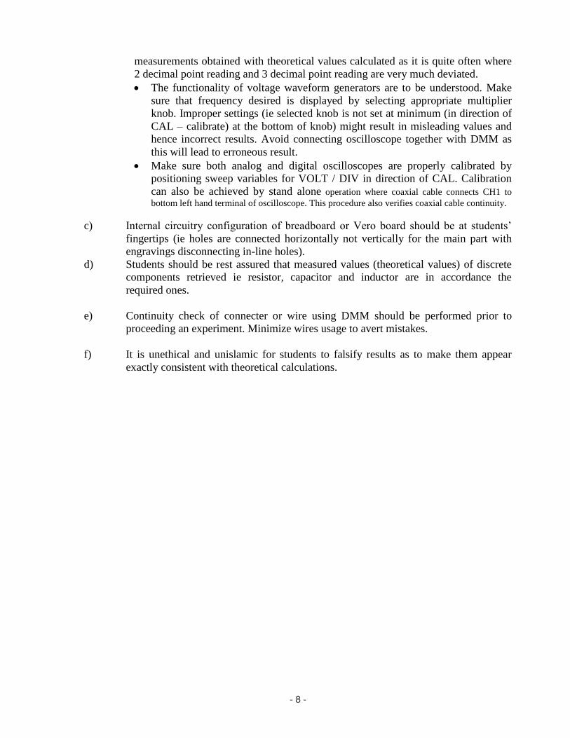
measurements obtained with theoretical values calculated as it is quite often where
2 decimal point reading and 3 decimal point reading are very much deviated.
The functionality of voltage waveform generators are to be understood. Make
sure that frequency desired is displayed by selecting appropriate multiplier
knob. Improper settings (ie selected knob is not set at minimum (in direction of
CAL – calibrate) at the bottom of knob) might result in misleading values and
hence incorrect results. Avoid connecting oscilloscope together with DMM as
this will lead to erroneous result.
Make sure both analog and digital oscilloscopes are properly calibrated by
positioning sweep variables for VOLT / DIV in direction of CAL. Calibration
can also be achieved by stand alone operation where coaxial cable connects CH1 to
bottom left hand terminal of oscilloscope. This procedure also verifies coaxial cable continuity.
c) Internal circuitry configuration of breadboard or Vero board should be at students’
fingertips (ie holes are connected horizontally not vertically for the main part with
engravings disconnecting in-line holes).
d) Students should be rest assured that measured values (theoretical values) of discrete
components retrieved ie resistor, capacitor and inductor are in accordance the
required ones.
e) Continuity check of connecter or wire using DMM should be performed prior to
proceeding an experiment. Minimize wires usage to avert mistakes.
f) It is unethical and unislamic for students to falsify results as to make them appear
exactly consistent with theoretical calculations.
- 9 -
INTRODUCTION TO ENGINEERING LAB II (ECE 1201) - ELECTRONICS
1. Basic Guidelines
2. Lab Instructions
3. Grading
4. Lab Reports
5. Schedule and Experiment No. (Title)
1. Basic Guidelines
All experiments in this manual have been tried and proven and should give you little trouble in
normal laboratory circumstances. However, a few guidelines will help you conduct the
experiments quickly and successfully.
1. Each experiment has been written so that you follow a structured logical sequence
meant to lead you to a specific set of conclusions. Be sure to follow the procedural
steps in the order which they are written.
2. Read the entire experiment and research any required theory beforehand. Many times
an experiment takes longer that one class period simply because a student is not well
prepared.
3. Once the circuit is connected, if it appears “dead’’ spend few moments checking for
obvious faults. Some common simple errors are: power not applied, switch off, faulty
components, lose connection, etc. Generally the problems are with the operator and not
the equipment.
4. When making measurements, check for their sensibility.
5. It’s unethical to “fiddle” or alter your results to make them appear exactly
consistent with theoretical calculations.
2. Lab Instructions
1. Each student group consists of a maximum of two students. Each group is responsible
in submitting 1 lab report upon completion of each experiment.
2. Students are to wear proper attire i.e shoe or sandal instead of slipper. Excessive
jewelleries are not advisable as they might cause electrical shock.
3. Personal belongings i.e bags, etc are to be put at the racks provided. Student groups are
required to wire up their circuits in accordance with the diagram given in each
experiment.
4. A permanent record in ink of observations as well as results should be maintained by
each student and enclosed with the report.
5. The recorded data and observations from the lab manual need to be approved and
signed by the lab instructor upon completion of each experiment.
6. Before beginning connecting up, it is essential to check that all sources of supply at the
bench are switched off.
7. Start connecting up the experiment circuit by wiring up the main circuit path, then add
the parallel branches as indicated in the circuit diagram.
8. After the circuit has been connected correctly, remove all unused leads from the
experiment area, set the voltage supplies at the minimum value, and check the meters
are set for the intended mode of operation.
9. The students may ask the lab instructor to check the correctness of their circuit before
switching on.
- 10 -
10. When the experiment has been satisfactory completed and the results approved by the
instructor, the students may disconnect the circuit and return the components and
instruments to the locker tidily. Chairs are to be slid in properly.
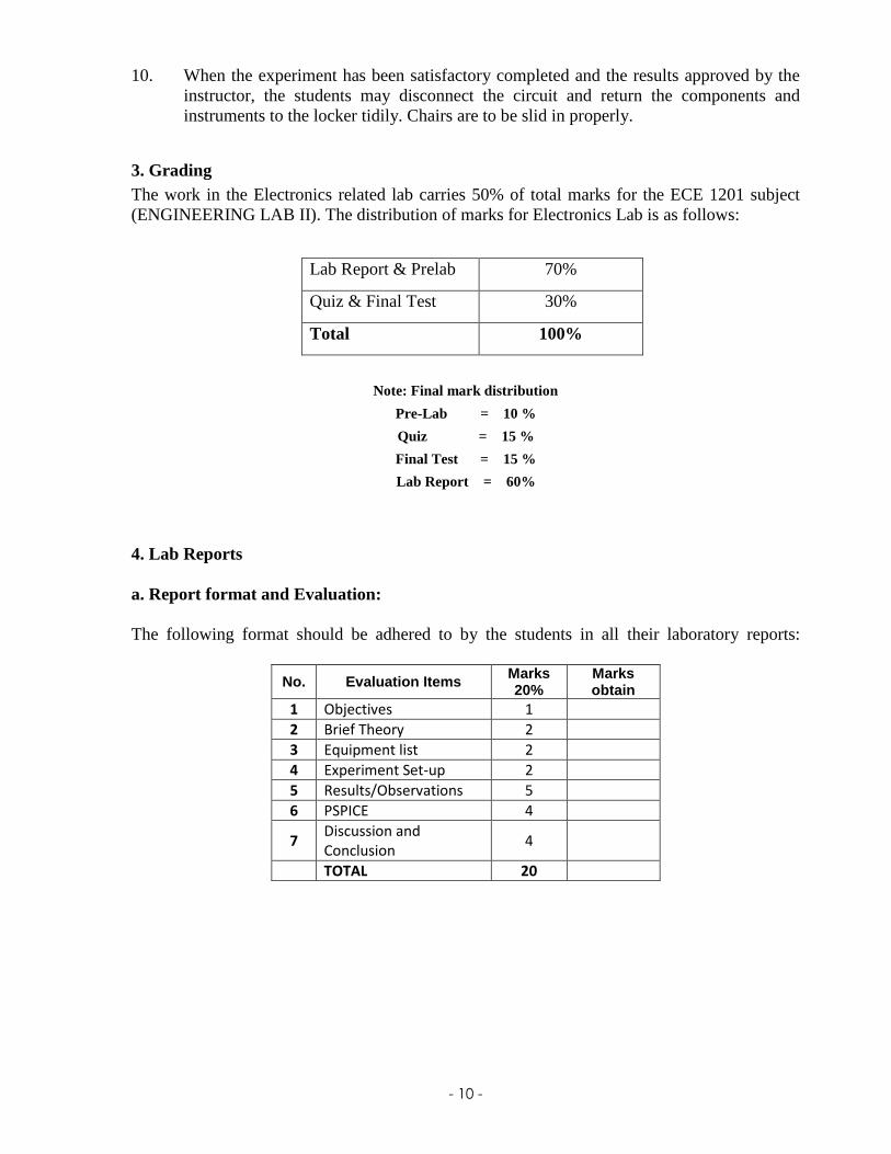
3. Grading
The work in the Electronics related lab carries 50% of total marks for the ECE 1201 subject
(ENGINEERING LAB II). The distribution of marks for Electronics Lab is as follows:
Lab Report & Prelab 70%
Quiz & Final Test 30%
Total 100%
Note: Final mark distribution
Pre-Lab = 10 %
Quiz = 15 %
Final Test = 15 %
Lab Report = 60%
4. Lab Reports
a. Report format and Evaluation:
The following format should be adhered to by the students in all their laboratory reports:
No. Evaluation Items Marks 20%
Marks obtain
1 Objectives 1
2 Brief Theory 2
3 Equipment list 2
4 Experiment Set-up 2
5 Results/Observations 5
6 PSPICE 4
7 Discussion and Conclusion
4
TOTAL 20
- 11 -
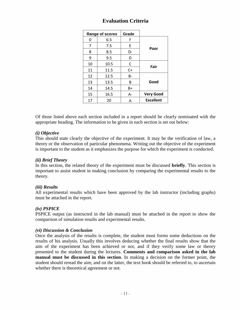
Evaluation Criteria
Range of scores Grade
0 6.5 F
Poor 7 7.5 E
8 8.5 D-
9 9.5 D
10 10.5 C Fair
11 11.5 C+
12 12.5 B- Good 13 13.5 B
14 14.5 B+
15 16.5 A- Very Good
17 20 A Excellent
Of those listed above each section included in a report should be clearly nominated with the
appropriate heading. The information to be given in each section is set out below:
(i) Objective
This should state clearly the objective of the experiment. It may be the verification of law, a
theory or the observation of particular phenomena. Writing out the objective of the experiment
is important to the student as it emphasizes the purpose for which the experiment is conducted.
(ii) Brief Theory
In this section, the related theory of the experiment must be discussed briefly. This section is
important to assist student in making conclusion by comparing the experimental results to the
theory.
(iii) Results
All experimental results which have been approved by the lab instructor (including graphs)
must be attached in the report.
(iv) PSPICE
PSPICE output (as instructed in the lab manual) must be attached in the report to show the
comparison of simulation results and experimental results.
(vi) Discussion & Conclusion
Once the analysis of the results is complete, the student must forms some deductions on the
results of his analysis. Usually this involves deducing whether the final results show that the
aim of the experiment has been achieved or not, and if they verify some law or theory
presented to the student during the lectures. Comments and comparison asked in the lab
manual must be discussed in this section. In making a decision on the former point, the
student should reread the aim; and on the latter, the text book should be referred to, to ascertain
whether there is theoretical agreement or not.
- 12 -
The student should give considerable thought to the material that he intends to submit in this
section. It is here that he is able to express his own ideas on the experiment results and how
they were obtained. It is the best indication to his teacher of whether he has understood the
experiment and of how well he has been able to analyze the results and make deductions from
them.
It is recommended that the conclusion should be taken up by the student’s clear and concise
explanation of his reasoning, based on the experimental results, that led to the deductions from
which he was able to make the two statements with which he began the conclusion.
It is very rare for an experiment to have results which are entirely without some discrepancy.
The student should explain what factors, in his opinion, may be the possible causes of these
discrepancies. Similarly, results of an unexpected nature should form the basis for a discussion
of their possible nature and cause.
The student should not be reluctant to give his opinions even though they may not be correct.
He should regard his discussion as an opportunity to demonstrate his reasoning ability.
Should the results obtained be incompatible with the aim or with the theory underlying the
experiment, then an acceptable report may be written suggesting reasons for the unsatisfactory
results. It is expected that the student should make some suggestions as to how similar
erroneous results for this experiment might be avoided in the future. The student must not form
the opinion that an unsatisfactory set of results makes a report unacceptable.
b. Presentation of Lab Reports:
All students are required to present their reports in accordance with the following instructions.
(i) Reports have to be handwritten for submission.
(ii) Writing should appear on one side of each sheet only.
(iii) The students’ name & matric number, section number, lab session and the lecturer’s
name must be printed in block letters at the top left-hand corner of the first sheet of the
report. This must be followed in the middle of the sheet by:
The course code
The experiment number
The title of the experiment
The date on which the student carried out the experiment.
(iv) All sections such as objective, brief theory and so on, should be titled on the left hand
side of the working space of the page.
- 13 -
(v)
Each type of calculation pertaining to the experiment should be preceded by a brief
statement indicating its objective.
All calculations are to be shown in sufficient details to enable the reader to follow their
procedure.
All formulas used are to be written in correct symbols prior to the substitution of the known
quantities.
(vi) All graphs are to be drawn on graph paper in blue or black ink. Other colors may be
used for identification. The abscissa and ordinate are to be drawn in all times and scaled
with the value clearly indicated at each major division. The quantity at each axis
represents and the unit in which it is calibrated should be clearly indicated. Each graph
is to be titled so as to indicate clearly what it represents.
(vii) The report submitted by each student should contain a conclusion and discussion of
more than 300 words.
(viii) The cover of the report must be as follows:
- 14 -
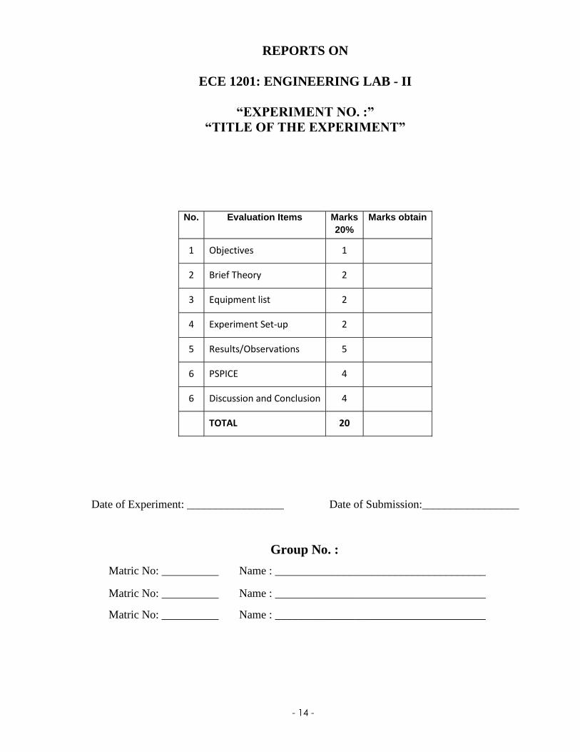
INTERNATIONAL ISLAMIC UNIVERSITY MALAYSIA
REPORTS ON
ECE 1201: ENGINEERING LAB - II
“EXPERIMENT NO. :”
“TITLE OF THE EXPERIMENT”
No. Evaluation Items Marks
20%
Marks obtain
1 Objectives 1
2 Brief Theory 2
3 Equipment list 2
4 Experiment Set-up 2
5 Results/Observations 5
6 PSPICE 4
6 Discussion and Conclusion 4
TOTAL 20
Date of Experiment: _________________ Date of Submission:_________________
Group No. :
Matric No: __________ Name : _____________________________________
Matric No: __________ Name : _____________________________________
Matric No: __________ Name : _____________________________________
- 15 -
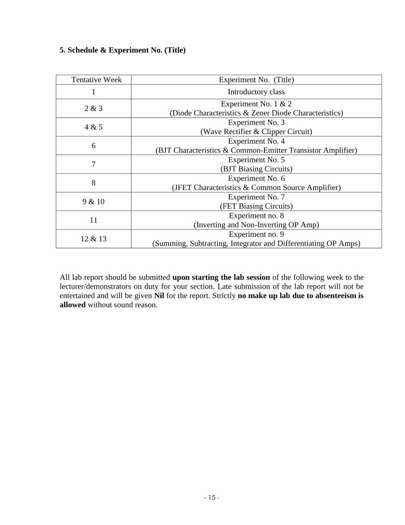
5. Schedule & Experiment No. (Title)
Tentative Week Experiment No. (Title)
1 Introductory class
2 & 3 Experiment No. 1 & 2
(Diode Characteristics & Zener Diode Characteristics)
4 & 5 Experiment No. 3
(Wave Rectifier & Clipper Circuit)
6 Experiment No. 4
(BJT Characteristics & Common-Emitter Transistor Amplifier)
7 Experiment No. 5
(BJT Biasing Circuits)
8 Experiment No. 6
(JFET Characteristics & Common Source Amplifier)
9 & 10 Experiment No. 7
(FET Biasing Circuits)
11 Experiment no. 8
(Inverting and Non-Inverting OP Amp)
12 & 13 Experiment no. 9
(Summing, Subtracting, Integrator and Differentiating OP Amps)
All lab report should be submitted upon starting the lab session of the following week to the
lecturer/demonstrators on duty for your section. Late submission of the lab report will not be
entertained and will be given Nil for the report. Strictly no make up lab due to absenteeism is
allowed without sound reason.
- 16 -
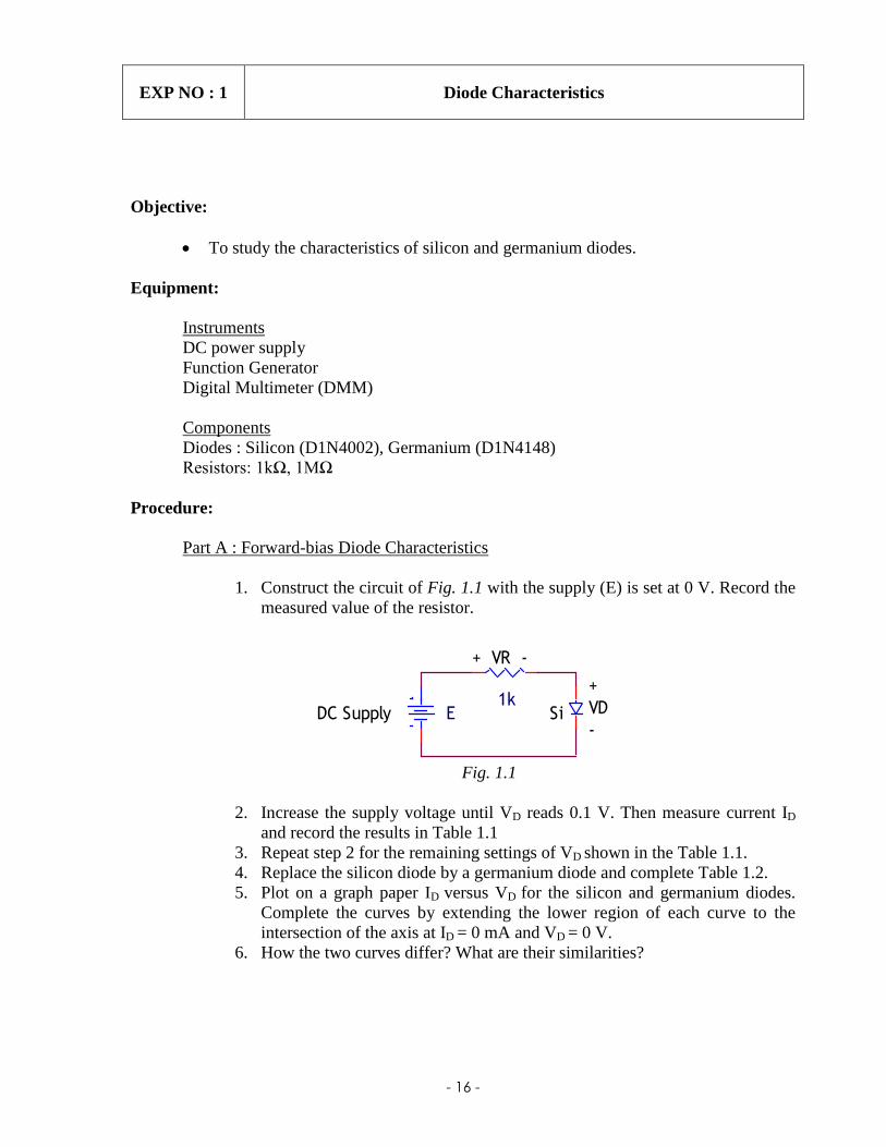
Objective:
To study the characteristics of silicon and germanium diodes.
Equipment:
Instruments
DC power supply
Function Generator
Digital Multimeter (DMM)
Components
Diodes : Silicon (D1N4002), Germanium (D1N4148)
Resistors: 1kΩ, 1MΩ
Procedure:
Part A : Forward-bias Diode Characteristics
1. Construct the circuit of Fig. 1.1 with the supply (E) is set at 0 V. Record the
measured value of the resistor.
Fig. 1.1
2. Increase the supply voltage until VD reads 0.1 V. Then measure current ID
and record the results in Table 1.1
3. Repeat step 2 for the remaining settings of VD shown in the Table 1.1.
4. Replace the silicon diode by a germanium diode and complete Table 1.2.
5. Plot on a graph paper ID versus VD for the silicon and germanium diodes.
Complete the curves by extending the lower region of each curve to the
intersection of the axis at ID = 0 mA and VD = 0 V.
6. How the two curves differ? What are their similarities?
EDC Supply Si
+
VD
-
1k
+ VR -
EXP NO : 1
Diode Characteristics
- 17 -
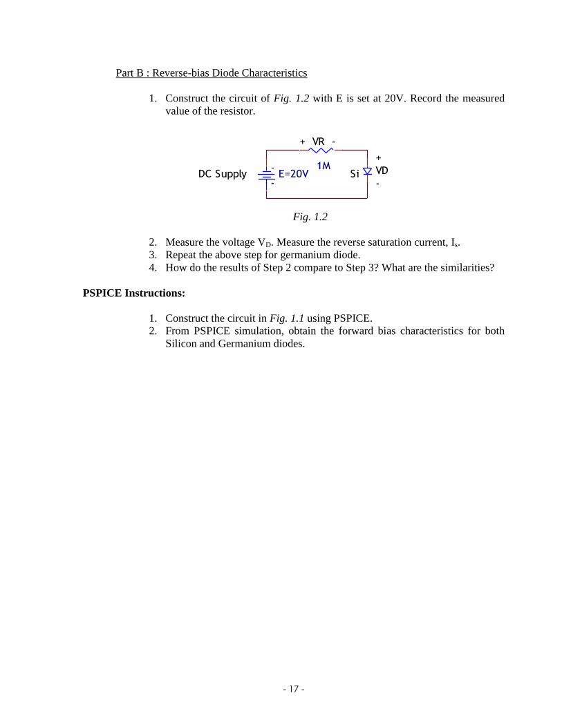
Part B : Reverse-bias Diode Characteristics
1. Construct the circuit of Fig. 1.2 with E is set at 20V. Record the measured
value of the resistor.
Fig. 1.2
2. Measure the voltage VD. Measure the reverse saturation current, Is.
3. Repeat the above step for germanium diode.
4. How do the results of Step 2 compare to Step 3? What are the similarities?
PSPICE Instructions:
1. Construct the circuit in Fig. 1.1 using PSPICE.
2. From PSPICE simulation, obtain the forward bias characteristics for both
Silicon and Germanium diodes.
E=20VDC Supply
+ VR -
1MSi
+
VD
-
- 18 -
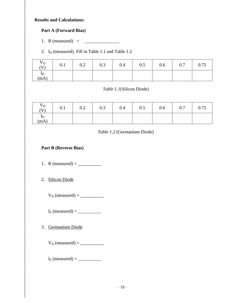
Results and Calculations:
Part A (Forward Bias)
1. R (measured) = _______________
2. ID (measured). Fill in Table 1.1 and Table 1.2
VD
(V) 0.1 0.2 0.3 0.4 0.5 0.6 0.7 0.75
ID
(mA)
Table 1.1(Silicon Diode)
VD
(V) 0.1 0.2 0.3 0.4 0.5 0.6 0.7 0.75
ID
(mA)
Table 1.2 (Germanium Diode)
Part B (Reverse Bias)
1. R (measured) = __________
2. Silicon Diode
VD (measured) = __________
IS (measured) = __________
3. Germanium Diode
VD (measured) = __________
IS (measured) = __________
----------------------------------------------------------------------------------------------------------------------------------------------------------------------------------------------------
- 19 -
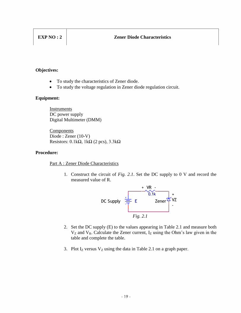
Objectives:
To study the characteristics of Zener diode.
To study the voltage regulation in Zener diode regulation circuit.
Equipment:
Instruments
DC power supply
Digital Multimeter (DMM)
Components
Diode : Zener (10-V)
Resistors: 0.1kΩ, 1kΩ (2 pcs), 3.3kΩ
Procedure:
Part A : Zener Diode Characteristics
1. Construct the circuit of Fig. 2.1. Set the DC supply to 0 V and record the
measured value of R.
Fig. 2.1
2. Set the DC supply (E) to the values appearing in Table 2.1 and measure both
VZ and VR. Calculate the Zener current, IZ using the Ohm’s law given in the
table and complete the table.
3. Plot IZ versus VZ using the data in Table 2.1 on a graph paper.
Zener
0.1k
+ VR -
EDC Supply
+
VZ
-
EXP NO : 2
Zener Diode Characteristics
- 20 -
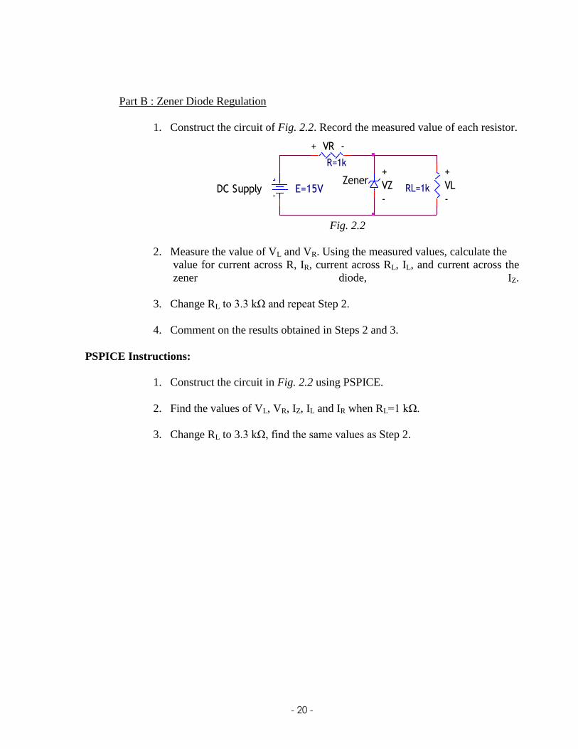
Part B : Zener Diode Regulation
1. Construct the circuit of Fig. 2.2. Record the measured value of each resistor.
Fig. 2.2
2. Measure the value of VL and VR. Using the measured values, calculate the
value for current across R, IR, current across RL, IL, and current across the
zener diode, IZ.
3. Change RL to 3.3 kΩ and repeat Step 2.
4. Comment on the results obtained in Steps 2 and 3.
PSPICE Instructions:
1. Construct the circuit in Fig. 2.2 using PSPICE.
2. Find the values of VL, VR, IZ, IL and IR when RL=1 kΩ.
3. Change RL to 3.3 kΩ, find the same values as Step 2.
E=15VDC Supply
+
VL
-
+ VR -
RL=1k
+
VZ
-
R=1k
Zener
- 21 -
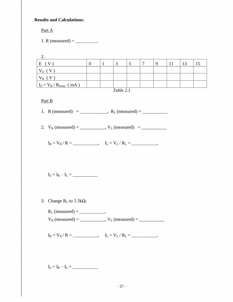
Results and Calculations:
Part A
1. R (measured) = __________
2.
E ( V ) 0 1 3 5 7 9 11 13 15
VZ ( V )
VR ( V )
IZ = VR / Rmeas ( mA )
Table 2.1
Part B
1. R (measured) = ____________, RL (measured) = ___________
2. VR (measured) = ___________, VL (measured) = ___________
IR = VR / R = ___________, IL = VL / RL = ___________,
IZ = IR – IL = ___________
3. Change RL to 3.3kΩ;
RL (measured) = ___________,
VR (measured) = ___________, VL (measured) = ___________
IR = VR / R = ___________, IL = VL / RL = ___________,
IZ = IR – IL = ___________
----------------------------------------------------------------------------------------------------------------------------------------------------------------------------------------------------
- 22 -
Objectives:
To calculate and draw the DC output voltages of half-wave and full-wave rectifiers.
To calculate and measure the output voltages of clipper circuits.
Equipment:
Instruments
DC power supply
AC power supply - ( Model : PSU-3097 ,12VAC ~0~ 12VAC ).
Digital Multimeter (DMM)
Function Generator
Oscilloscope
Components
Diode : Silicon ( D1N4002 )
Resistors: 2.2kΩ, 3.3kΩ
Procedure:
Part A : Half Wave Rectification
1. Construct the circuit of Fig. 3.1. Set the supply to 9 V p-p sinusoidal wave
with the frequency of 1000 Hz. Put the oscilloscope probes at function
generator and sketch the input waveform obtained.
2. Put the oscilloscope probes across the resistor and sketch the output
waveform obtained. Measure and record the DC level of the output voltage
using the DMM.
Fig. 3.1
3. Reverse the diode of circuit of Fig. 3.1. Sketch the output waveform across
the resistor. Measure and record the DC level of the output voltage.
4. Comment on the results obtained from step 2 and 3.
EXP NO: 3
Wave Rectifier and Clipper Circuits
Function
Generator
- 23 -
Part B : Full-Wave Rectification
1. Construct the circuit of Fig. 3.2. with 12VAC , AC Power Supply.
( Model : PSU-3097 ,12VAC ~0~ 12VAC ).
2. Put the oscilloscope probes across the resistor and sketch the output
waveform obtained. Measure and record the DC level of the output voltage
using the DMM.
Fig. 3.2
3. Replace diodes D3 and D4 of circuit of Fig. 3.2 by 2.2 kΩ. Draw the output
waveform across the resistor. Measure and record the DC level of the output
voltage.
4. What is the major effect of replacing the two diodes (D3 and D4) with
resistors?
Part C : Parallel Clippers
1. Construct the circuit in Fig. 3.3. The input signal is an 8 V p-p square wave
at frequency of 1000 Hz. Record the measured resistance value.
2. Set the oscilloscope in DC mode.
3. Put the oscilloscope probes at function generator and sketch the input
waveform obtained.
Fig. 3.3
4. Sketch the output waveform obtained from the oscilloscope.
5. Reverse the battery of the circuit and sketch the output waveform.
6. How do the waveforms differ? What is the function of the battery in the
circuit?
7. Change the input signal of the circuit of Fig. 3.3 to an 8 V p-p sinusoidal
signal with the same frequency of 1000 Hz. Repeat step 3 and 4 for this
circuit.
Function
Generator
DC Supply
AC Power
Supply 12VAC
(PSU-3097)
- 24 -
Part D : Series Clippers
1. Construct the circuit in Fig. 3.4. The input signal is an 8 V p-p square wave
at frequency of 1000 Hz. Record the measured resistance value.
2. Set the oscilloscope in DC mode.
3. Put the oscilloscope probes at function generator and sketch the input
waveform obtained.
Fig. 3.4
4. Sketch the output waveform obtained from the oscilloscope.
5. Reverse the battery of the circuit and sketch the output waveform.
6. Change the input signal of the circuit of Fig. 3.4 to an 8 V p-p sinusoidal
signal with the same frequency of 1000 Hz. Repeat step 3 and 4 for this
circuit.
7. How does the series clipper differ from the parallel clipper?
PSPICE Instructions:
Get the expected output waveform for circuits in Fig. 3.1 (Part A) & Fig. 3.3 (Part C) using
PSPICE Simulation.
Function
Generator
DC Supply
- 25 -
Results and Calculations:
Part A
1. Input waveform, Vi :
2. Output waveform, Vo :
DC level of Vo (measured) = __________
Part A (reversed diode)
3. Output waveform, Vo :
DC level of Vo (measured) = __________
--------------------------------------------------------------------------------------------------------------------------------------------------------------------------------------------------
V(volt)
Time (s)
V(volt)
Time (s)
V(volt)
Time (s)
- 26 -
Part B
1. Input waveform, Vi :
2. Output waveform, Vo :
DC level of Vo (measured) = __________
Part B (diodes replaced with resistors)
3. Output waveform, Vo :
DC level of Vo (measured) = __________
V(volt)
Time (s)
V(volt)
Time (s)
V(volt)
Time (s)
----------------------------------------------------------------------------------------------------------------------------------------------------------------------------------------------------
- 27 -
Part C (vin square-wave)
1. R (measured) = _______________
2. Input waveform :
3. Output waveform :
Part C (vin square-wave, battery reversed)
4. Output waveform :
V(volt)
Time (s)
V(volt)
Time (s)
----------------------------------------------------------------------------------------------------------------------------------------------------------------------------------------------------
V(volt)
Time (s)
- 28 -
Part C (vin sine-wave)
5. Input waveform :
6. Output waveform :
Part C (vin sine-wave, battery reversed)
7. Output waveform :
V(volt)
Time (s)
V(volt)
Time (s)
V(volt)
Time (s)
----------------------------------------------------------------------------------------------------------------------------------------------------------------------------------------------------
- 29 -
Part D (vin square-wave)
1. R (measured) = _______________
2. Input waveform :
3. Output waveform :
Part D (vin square-wave, battery reversed)
4. Output waveform :
V(volt)
Time (s)
V(volt)
Time (s)
V(volt)
Time (s)
- 30 -
Part D (vin sine-wave)
5. Input waveform :
6. Output waveform :
Part D (vin sine-wave, battery reversed)
7. Output waveform :
V(volt)
Time (s)
V(volt)
Time (s)
V(volt)
Time (s)
- 31 -
Objectives:
To graph the collector characteristics of a transistor using experimental methods.
To measure AC and DC voltages in a common-emitter amplifier.
Equipment:
Instruments
1 DC Power Supply
3 Digital Multimeter (DMM)
1 Function Generator
1 Oscilloscope
Components
Resistors: 1 k, 3 k, 10 k, 33 k, 330 k, 10 k potentiometer, 1M
potentiometer
Transistors: 2N3904
Procedure:
Part A : The Collector Characteristics (BJT)
1. Construct the circuit of Fig. 4.1. Vary the 1M potentiometer to set IB = 10
A as in Table 4.1.
Fig. 4.1
2. Set the VCE to 2V by varying the 10k potentiometer as required by the first
line of Table 4.1.
3. Record the VRC and VBE values in Table 4.1.
1M
A- VRC +
Base
20V
Collector
C
CRB=330k
10k
Emitter
ARC=1k
B
B
EXP NO: 4
BJT Characteristics & Common-Emitter Transistor Amplifier
IB
DC Supply
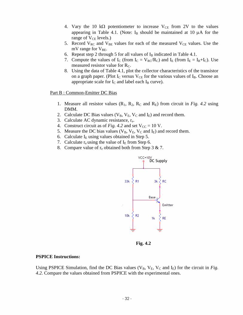
- 32 -
4. Vary the 10 k potentiometer to increase VCE from 2V to the values
appearing in Table 4.1. (Note: IB should be maintained at 10 A for the
range of VCE levels.)
5. Record VRC and VBE values for each of the measured VCE values. Use the
mV range for VBE.
6. Repeat step 2 through 5 for all values of IB indicated in Table 4.1.
7. Compute the values of IC (from IC = VRC/RC) and IE (from IE = IB+IC). Use
measured resistor value for RC.
8. Using the data of Table 4.1, plot the collector characteristics of the transistor
on a graph paper. (Plot IC versus VCE for the various values of IB. Choose an
appropriate scale for IC and label each IB curve).
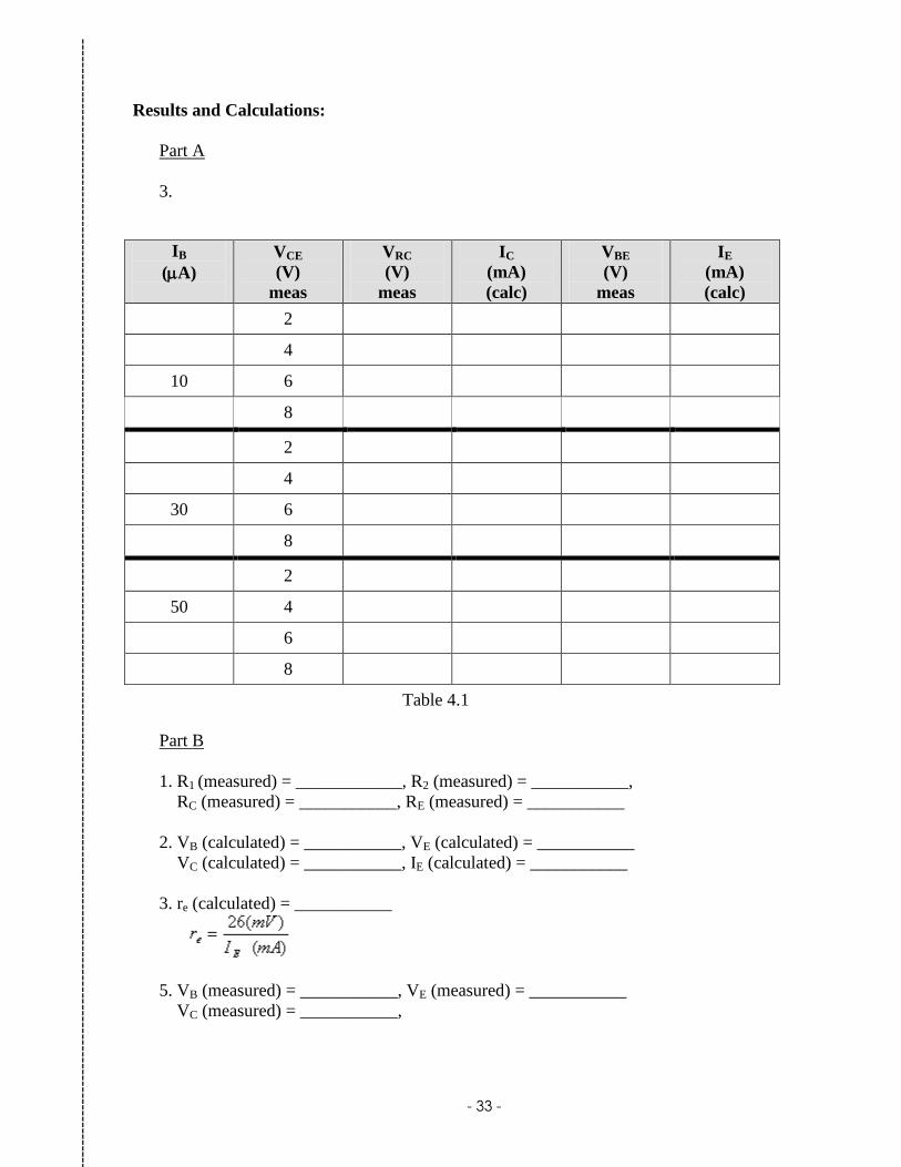
Part B : Common-Emitter DC Bias
1. Measure all resistor values (R1, R2, RC and RE) from circuit in Fig. 4.2 using
DMM.
2. Calculate DC Bias values (VB, VE, VC and IE) and record them.
3. Calculate AC dynamic resistance, re.
4. Construct circuit as of Fig. 4.2 and set VCC = 10 V.
5. Measure the DC bias values (VB, VE, VC and IE) and record them.
6. Calculate IE using values obtained in Step 5.
7. Calculate re using the value of IE from Step 6.
8. Compare value of re obtained both from Step 3 & 7.
Fig. 4.2
PSPICE Instructions:
Using PSPICE Simulation, find the DC Bias values (VB, VE, VC and IE) for the circuit in Fig.
4.2. Compare the values obtained from PSPICE with the experimental ones.
DC Supply
- 33 -
Results and Calculations:
Part A
3.
Table 4.1
Part B
1. R1 (measured) = ____________, R2 (measured) = ___________,
RC (measured) = ___________, RE (measured) = ___________
2. VB (calculated) = ___________, VE (calculated) = ___________
VC (calculated) = ___________, IE (calculated) = ___________
3. re (calculated) = ___________
5. VB (measured) = ___________, VE (measured) = ___________
VC (measured) = ___________,
IB
(A)
VCE
(V)
meas
VRC
(V)
meas
IC
(mA)
(calc)
VBE
(V)
meas
IE
(mA)
(calc)
2
4
10 6
8
2
4
30 6
8
2
50 4
6
8
----------------------------------------------------------------------------------------------------------------------------------------------------------------------------------------------------

- 34 -
6. IE (calculated) using measured values of VE and RE = __________
EEE RVI /
7. re (measured) = ____________, using IE from Step 6.
8. Graph IC versus VCE for each value of IB (use graph paper).
- 35 -
Objectives:
To determine the quiescent operating conditions of the fixed- and voltage-divider-bias BJT
configurations.
Equipment:
Instruments
1 DC Power Supply
3 Digital Multimeter (DMM)
Components
Resistors: 680 , 1.8 k, 2.7 k, 6.8 k, 33 k, 1 M
Transistors: 2N3904, 2N4401
Procedure:
Part A : Fixed-Bias Configuration
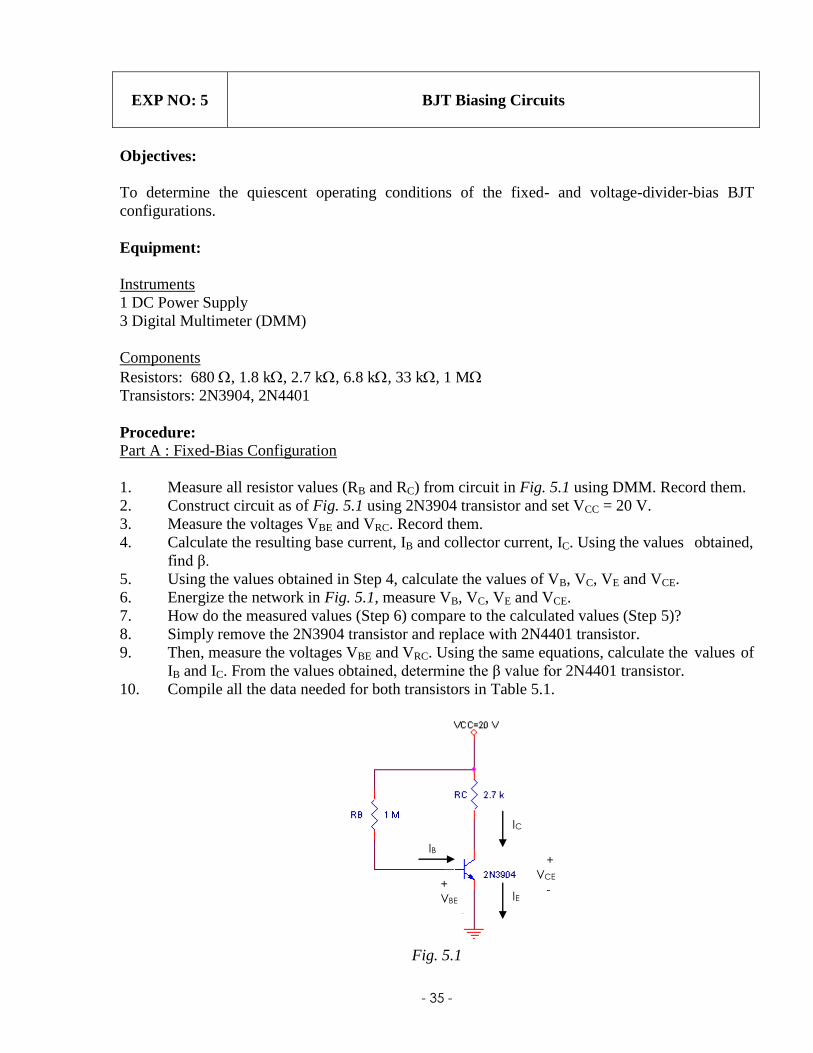
1. Measure all resistor values (RB and RC) from circuit in Fig. 5.1 using DMM. Record them.
2. Construct circuit as of Fig. 5.1 using 2N3904 transistor and set VCC = 20 V.
3. Measure the voltages VBE and VRC. Record them.
4. Calculate the resulting base current, IB and collector current, IC. Using the values obtained,
find β.
5. Using the values obtained in Step 4, calculate the values of VB, VC, VE and VCE.
6. Energize the network in Fig. 5.1, measure VB, VC, VE and VCE.
7. How do the measured values (Step 6) compare to the calculated values (Step 5)?
8. Simply remove the 2N3904 transistor and replace with 2N4401 transistor.
9. Then, measure the voltages VBE and VRC. Using the same equations, calculate the values of
IB and IC. From the values obtained, determine the β value for 2N4401 transistor.
10. Compile all the data needed for both transistors in Table 5.1.
Fig. 5.1
EXP NO: 5
BJT Biasing Circuits
IB
IC
IE +
VBE
-
+
VCE
-
- 36 -
11. Calculate the magnitude (ignore the sign) of the percent change in each quantity due to a
change in transistors.
12. Place the results of your calculations in Table 5.2.
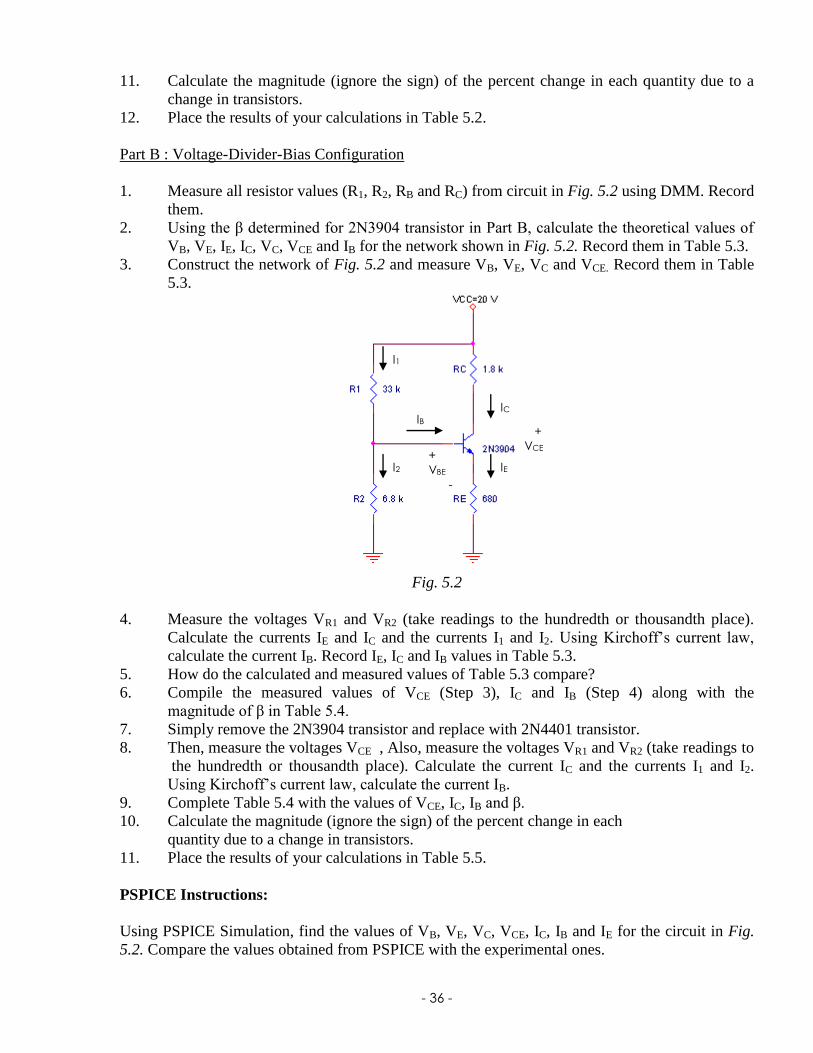
Part B : Voltage-Divider-Bias Configuration
1. Measure all resistor values (R1, R2, RB and RC) from circuit in Fig. 5.2 using DMM. Record
them.
2. Using the β determined for 2N3904 transistor in Part B, calculate the theoretical values of
VB, VE, IE, IC, VC, VCE and IB for the network shown in Fig. 5.2. Record them in Table 5.3.
3. Construct the network of Fig. 5.2 and measure VB, VE, VC and VCE. Record them in Table
5.3.
Fig. 5.2
4. Measure the voltages VR1 and VR2 (take readings to the hundredth or thousandth place).
Calculate the currents IE and IC and the currents I1 and I2. Using Kirchoff’s current law,
calculate the current IB. Record IE, IC and IB values in Table 5.3.
5. How do the calculated and measured values of Table 5.3 compare?
6. Compile the measured values of VCE (Step 3), IC and IB (Step 4) along with the
magnitude of β in Table 5.4.
7. Simply remove the 2N3904 transistor and replace with 2N4401 transistor.
8. Then, measure the voltages VCE , Also, measure the voltages VR1 and VR2 (take readings to
the hundredth or thousandth place). Calculate the current IC and the currents I1 and I2.
Using Kirchoff’s current law, calculate the current IB.
9. Complete Table 5.4 with the values of VCE, IC, IB and β.
10. Calculate the magnitude (ignore the sign) of the percent change in each
quantity due to a change in transistors.
11. Place the results of your calculations in Table 5.5.
PSPICE Instructions:
Using PSPICE Simulation, find the values of VB, VE, VC, VCE, IC, IB and IE for the circuit in Fig.
5.2. Compare the values obtained from PSPICE with the experimental ones.
I1
I2
IB
IC
IE
+
VBE
-
+
VCE
-
- 37 -
Results and Calculations:
Part A
1. RB (measured) = ______________, RC (measured) = _______________
3. VBE (measured) = ______________, VRC (measured) = ______________
4. IB = __________________, IC = _________________, β = _____________
B
BECC
B
RBB
R
VV
R
VI
C
RCC
R
VI
B
C
I
I
5. VB (calculated) = _____________, VC (calculated) = _______________
VE (calculated) = _____________, VCE (calculated) = ______________
Show your works!
6. VB (measured) = _____________, VC (measured) = _______________
VE (measured) = _____________, VCE (measured) = ______________
7. Comparison of results from Step 5 & Step 6 :
----------------------------------------------------------------------------------------------------------------------------------------------------------------------------------------------------
- 38 -
9. VBE (measured) = ______________, VRC (measured) = ______________
IB = __________________, IC = _________________, β = _____________
B
BECC
B
RBB
R
VV
R
VI
C
RCC
R
VI
B
C
I
I
10.
Trans. Type VCE (V) IC (mA) IB (μA) β
2N3904
2N4401
Table 5.1
11.
%100%3904
39044401
x
%100%
3904
39044401
xI
III
C
CC
C
%100%
3904
39044401
xV
VVV
CE
CECE
CE
%100%
3904
39044401
xI
III
B
BB
B
----------------------------------------------------------------------------------------------------------------------------------------------------------------------------------------------------

- 39 -
12.
Table 5.2
Part B
1. R1 (measured) = ____________, R2 (measured) = ___________,
RC (measured) = ___________, RE (measured) = ___________
2. VB (calculated) = ___________, VE (calculated) = ___________
IE (calculated) = ___________, IC (calculated) = ___________
VC (calculated) = ___________, VCE (calculated) = __________
IB (calculated) = ____________
Show your works!
%Δβ %ΔIC %ΔVCE %ΔIB
----------------------------------------------------------------------------------------------------------------------------------------------------------------------------------------------------
- 40 -
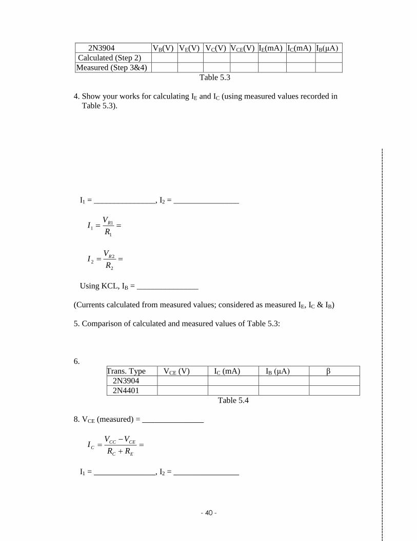
2N3904 VB(V) VE(V) VC(V) VCE(V) IE(mA) IC(mA) IB(μA)
Calculated (Step 2)
Measured (Step 3&4)
Table 5.3
4. Show your works for calculating IE and IC (using measured values recorded in
Table 5.3).
I1 = _______________, I2 = ________________
1
11
R
VI R
2
22
R
VI R
Using KCL, IB = _______________
(Currents calculated from measured values; considered as measured IE, IC & IB)
5. Comparison of calculated and measured values of Table 5.3:
6.
Trans. Type VCE (V) IC (mA) IB (μA) β
2N3904
2N4401
Table 5.4
8. VCE (measured) = _______________
EC
CECCC
RR
VVI
I1 = _______________, I2 = ________________
----------------------------------------------------------------------------------------------------------------------------------------------------------------------------------------------------
- 41 -
1
11
R
VI R
2
22
R
VI R
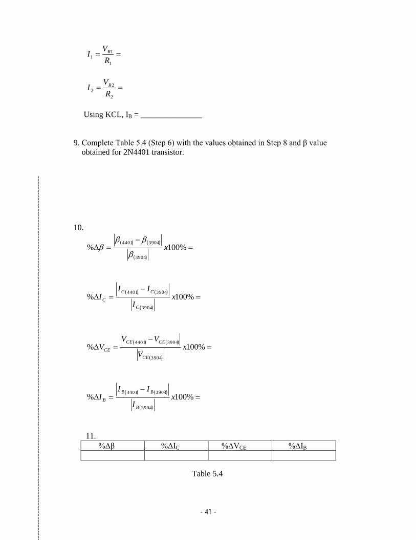
Using KCL, IB = _______________
9. Complete Table 5.4 (Step 6) with the values obtained in Step 8 and β value
obtained for 2N4401 transistor.
10.
%100%3904
39044401
x
%100%
3904
39044401
xI
III
C
CC
C
%100%
3904
39044401
xV
VVV
CE
CECE
CE
%100%
3904
39044401
xI
III
B
BB
B
11.
Table 5.4
%Δβ %ΔIC %ΔVCE %ΔIB
----------------------------------------------------------------------------------------------------------------------------------------------------------------------------------------------------
- 42 -
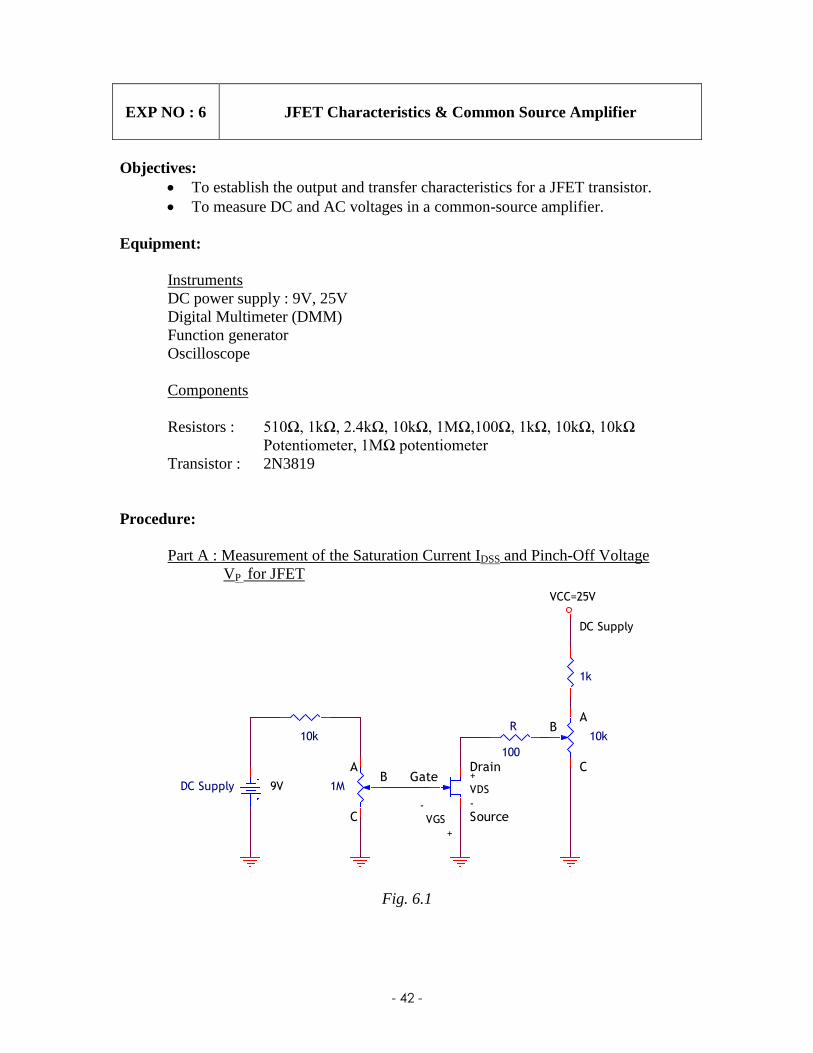
Objectives:
To establish the output and transfer characteristics for a JFET transistor.
To measure DC and AC voltages in a common-source amplifier.
Equipment:
Instruments
DC power supply : 9V, 25V
Digital Multimeter (DMM)
Function generator
Oscilloscope
Components
Resistors : 510Ω, 1kΩ, 2.4kΩ, 10kΩ, 1MΩ,100Ω, 1kΩ, 10kΩ, 10kΩ
Potentiometer, 1MΩ potentiometer
Transistor : 2N3819
Procedure:
Part A : Measurement of the Saturation Current IDSS and Pinch-Off Voltage
VP for JFET
Fig. 6.1
C
10k
-
VGS
+
R
100
1k
GateA C
DC Supply
VCC=25V
10k
A
DC Supply 9V
B
1MB
Drain
Source
+
VDS
-
EXP NO : 6
JFET Characteristics & Common Source Amplifier
- 43 -
1. Referring to Fig. 6.1, construct the circuit. The function of 10kΩ resistor in the
input circuit is to protect the circuit if the 9V supply is connected with wrong
polarity and the potentiometer is set on its maximum value.
2. Measure R value.
3. Set VDS to 8V by varying the 10kΩ potentiometer. Measure the voltage across R,
VR.
4. Vary the 1MΩ potentiometer until VGS = 0V. Measure ID at this time. (ID = IDSS
when VGS = 0V). Record ID measured.
5. Calculate the saturation current, IDSS using the measured resistor, R and VR
values. Record IDSS calculated.
6. Maintain VDS at about 8V and reduce VGS until VR drops to 1mV. At this level, ID
= VR/R = 1mV/100Ω = 10µA ≈ 0 mA. Record VGS value. The VGS value (when ID
is 0 mA) is the pinch-off voltage VP.
7. Using the values of IDSS and VP, sketch the transfer characteristics for the device
using Shockley’s equation given (in the results section). Plot at least 5 points on
the curve. (Use VP < VGS < 0V)
Part B : Output Characteristics (JFET)
1. Referring to Fig. 6.1, vary the two potentiometers until VGS = 0V and VDS = 0V.
Determine ID from ID = VR/R using the measured value of R and record in Table
6.1.
2. Maintain VGS at 0V and increase VDS from 0 to 14V and record the calculated
value of ID at every 1V increment (refer to Table 6.1). (Be sure to use the
measured value of R in your calculations)
3. Vary the 1MΩ potentiometer until VGS = -1V. Maintaining VGS at -1V, vary VDS
through the levels of Table 6.1 and record the calculated value of ID.
4. Repeat Step 3 for the values of VGS in Table 6.1. Discontinue the process if VGS
exceeds VP.
5. Plot the output characteristics for the JFET.
6. Compare the IDSS and VP values obtained from Step 5 with those measured in Part
A. Give comments.
Part C : Transfer Characteristics (JFET)
1. Using the data from Table 6.1, record the values of ID for the range of VGS at VDS
= 3V in Table 6.2.
2. Repeat step 1 for VDS = 6V, 9V and 12V.
3. For each level of VDS, plot ID vs VGS on the graph. Plot each curve carefully and
label each curve with the value of VDS.
- 44 -
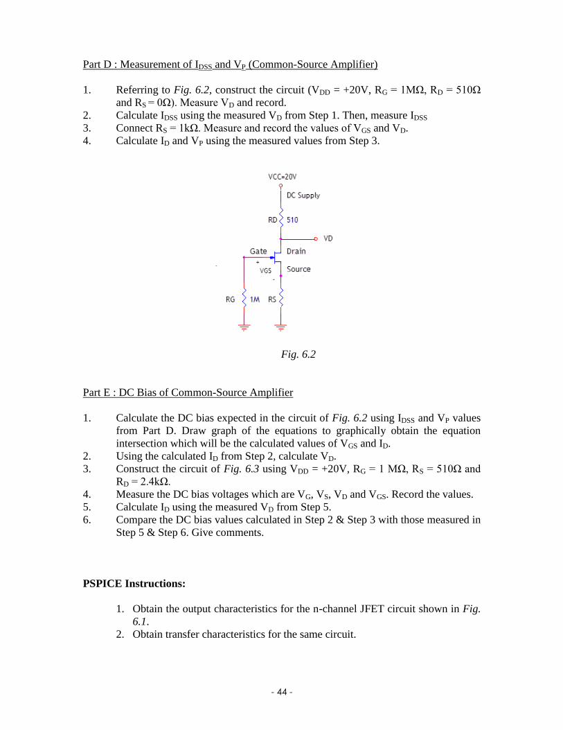
Part D : Measurement of IDSS and VP (Common-Source Amplifier)
1. Referring to Fig. 6.2, construct the circuit (VDD = +20V, RG = 1MΩ, RD = 510Ω
and RS = 0Ω). Measure VD and record.
2. Calculate IDSS using the measured VD from Step 1. Then, measure IDSS
3. Connect RS = 1kΩ. Measure and record the values of VGS and VD.
4. Calculate ID and VP using the measured values from Step 3.
Fig. 6.2
Part E : DC Bias of Common-Source Amplifier
1. Calculate the DC bias expected in the circuit of Fig. 6.2 using IDSS and VP values
from Part D. Draw graph of the equations to graphically obtain the equation
intersection which will be the calculated values of VGS and ID.
2. Using the calculated ID from Step 2, calculate VD.
3. Construct the circuit of Fig. 6.3 using VDD = +20V, RG = 1 MΩ, RS = 510Ω and
RD = 2.4kΩ.
4. Measure the DC bias voltages which are VG, VS, VD and VGS. Record the values.
5. Calculate ID using the measured VD from Step 5.
6. Compare the DC bias values calculated in Step 2 & Step 3 with those measured in
Step 5 & Step 6. Give comments.
PSPICE Instructions:
1. Obtain the output characteristics for the n-channel JFET circuit shown in Fig.
6.1.
2. Obtain transfer characteristics for the same circuit.
- 45 -
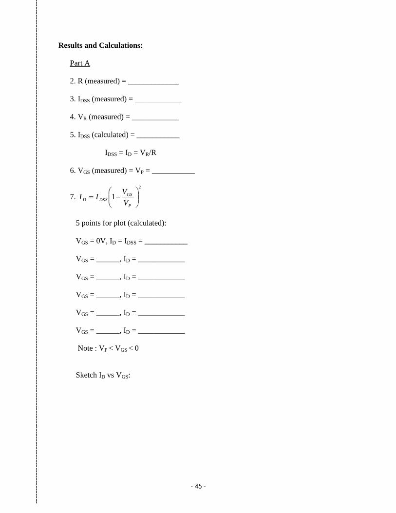
Results and Calculations:
Part A
2. R (measured) = _____________
3. IDSS (measured) = ____________
4. VR (measured) = ____________
5. IDSS (calculated) = ___________
IDSS = ID = VR/R
6. VGS (measured) = VP = ___________
7.
2
1
P
GS
DSSDV
VII
5 points for plot (calculated):
VGS = 0V, ID = IDSS = ___________
VGS = ______, ID = ____________
VGS = ______, ID = ____________
VGS = ______, ID = ____________
VGS = ______, ID = ____________
VGS = ______, ID = ____________
Note : VP < VGS < 0
Sketch ID vs VGS:
----------------------------------------------------------------------------------------------------------------------------------------------------------------------------------------------------
- 46 -
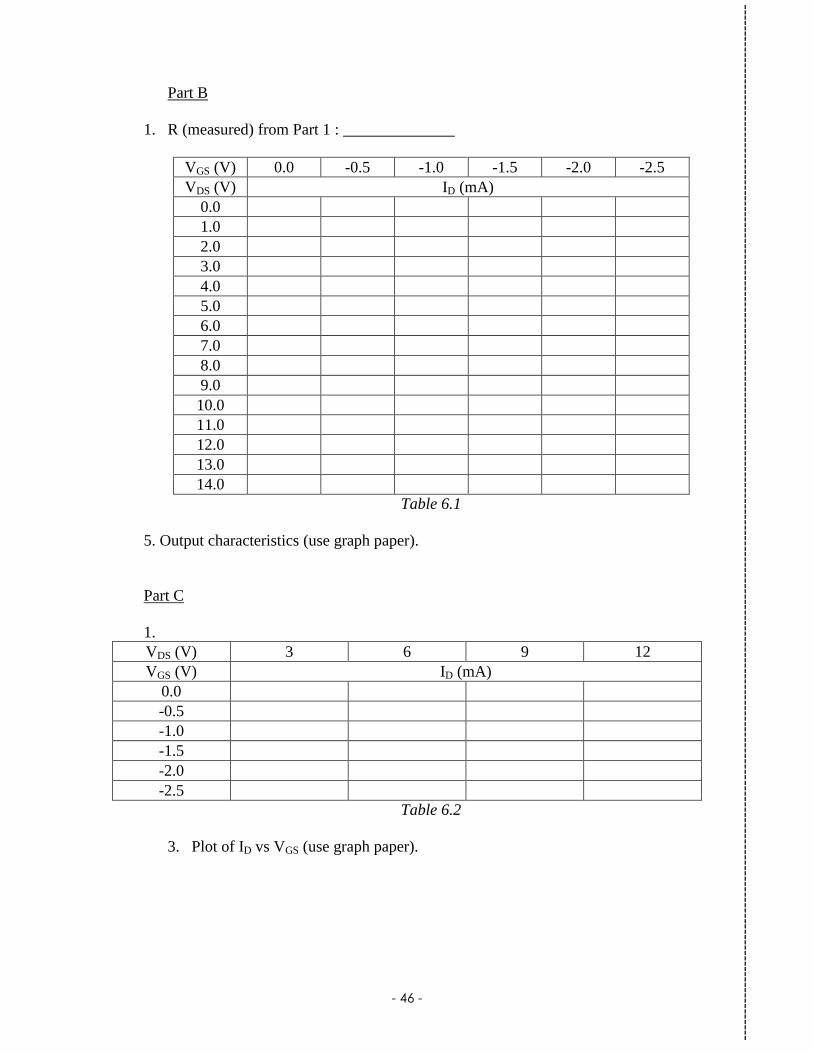
Part B
1. R (measured) from Part 1 : ______________
VGS (V) 0.0 -0.5 -1.0 -1.5 -2.0 -2.5
VDS (V) ID (mA)
0.0
1.0
2.0
3.0
4.0
5.0
6.0
7.0
8.0
9.0
10.0
11.0
12.0
13.0
14.0
Table 6.1
5. Output characteristics (use graph paper).
Part C
1.
VDS (V) 3 6 9 12
VGS (V) ID (mA)
0.0
-0.5
-1.0
-1.5
-2.0
-2.5
Table 6.2
3. Plot of ID vs VGS (use graph paper).
---------------------------------------------------------------------------------------------------------------------------------------------------------------------------------------------------
- 47 -
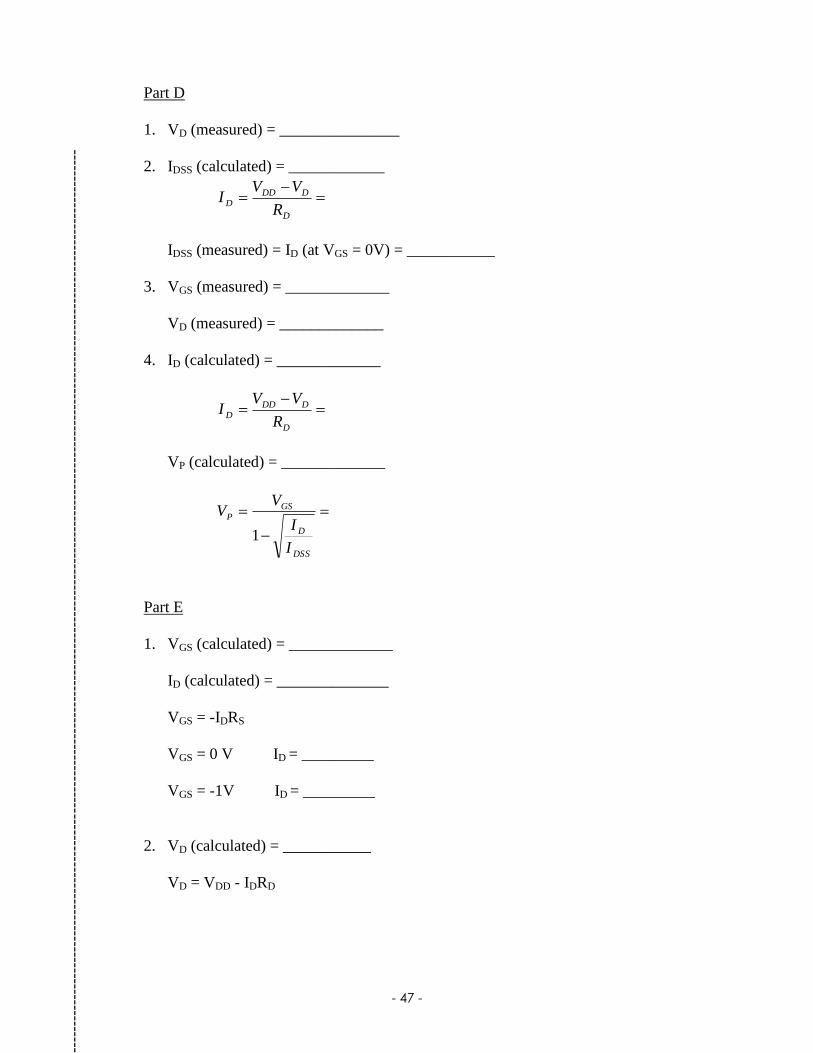
Part D
1. VD (measured) = _______________
2. IDSS (calculated) = ____________
D
DDDD
R
VVI
IDSS (measured) = ID (at VGS = 0V) = ___________
3. VGS (measured) = _____________
VD (measured) = _____________
4. ID (calculated) = _____________
D
DDDD
R
VVI
VP (calculated) = _____________
DSS
D
GS
P
I
I
VV
1
Part E
1. VGS (calculated) = _____________
ID (calculated) = ______________
VGS = -IDRS
VGS = 0 V ID = _________
VGS = -1V ID = _________
2. VD (calculated) = ___________
VD = VDD - IDRD
----------------------------------------------------------------------------------------------------------------------------------------------------------------------------------------------------
- 48 -
4. VG = __________
VS = __________
VD = __________
VGS = __________
5. ID (calculated) = ___________
ID = VS / RS
----------------------------------------------------------------------------------------------------------------------------------------------------------------------------------------------------
- 49 -
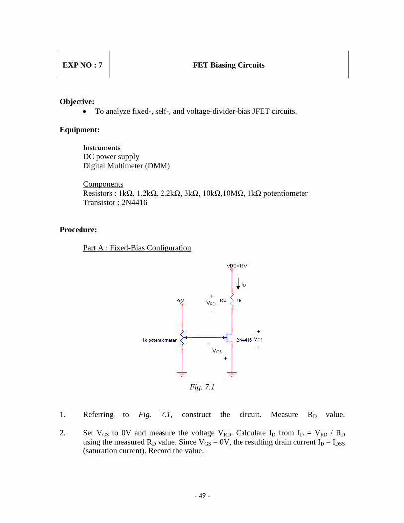
Objective:
To analyze fixed-, self-, and voltage-divider-bias JFET circuits.
Equipment:
Instruments
DC power supply
Digital Multimeter (DMM)
Components
Resistors : 1kΩ, 1.2kΩ, 2.2kΩ, 3kΩ, 10kΩ,10MΩ, 1kΩ potentiometer
Transistor : 2N4416
Procedure:
Part A : Fixed-Bias Configuration
Fig. 7.1
1. Referring to Fig. 7.1, construct the circuit. Measure RD value.
2. Set VGS to 0V and measure the voltage VRD. Calculate ID from ID = VRD / RD
using the measured RD value. Since VGS = 0V, the resulting drain current ID = IDSS
(saturation current). Record the value.
EXP NO : 7
FET Biasing Circuits
-
VGS
+
+
VDS
-
+
VRD
-
ID
- 50 -
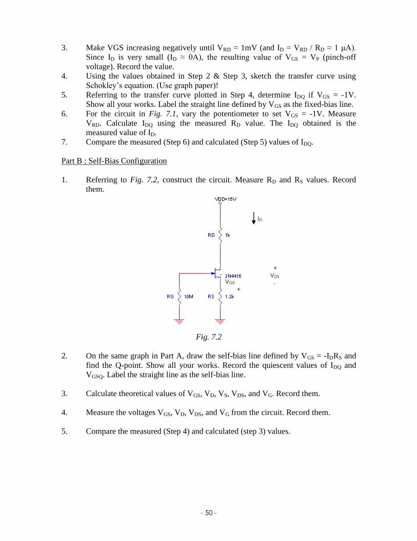
3. Make VGS increasing negatively until VRD = 1mV (and ID = VRD / RD ≈ 1 μA).
Since ID is very small (ID ≈ 0A), the resulting value of VGS = VP (pinch-off
voltage). Record the value.
4. Using the values obtained in Step 2 & Step 3, sketch the transfer curve using
Schokley’s equation. (Use graph paper)!
5. Referring to the transfer curve plotted in Step 4, determine IDQ if VGS = -1V.
Show all your works. Label the straight line defined by VGS as the fixed-bias line.
6. For the circuit in Fig. 7.1, vary the potentiometer to set VGS = -1V. Measure
VRD. Calculate IDQ using the measured RD value. The IDQ obtained is the
measured value of ID.
7. Compare the measured (Step 6) and calculated (Step 5) values of IDQ.
Part B : Self-Bias Configuration
1. Referring to Fig. 7.2, construct the circuit. Measure RD and RS values. Record
them.
Fig. 7.2
2. On the same graph in Part A, draw the self-bias line defined by VGS = -IDRS and
find the Q-point. Show all your works. Record the quiescent values of IDQ and
VGSQ. Label the straight line as the self-bias line.
3. Calculate theoretical values of VGS, VD, VS, VDS, and VG. Record them.
4. Measure the voltages VGS, VD, VDS, and VG from the circuit. Record them.
5. Compare the measured (Step 4) and calculated (step 3) values.
-
VGS
+
+
VDS
-
ID
- 51 -
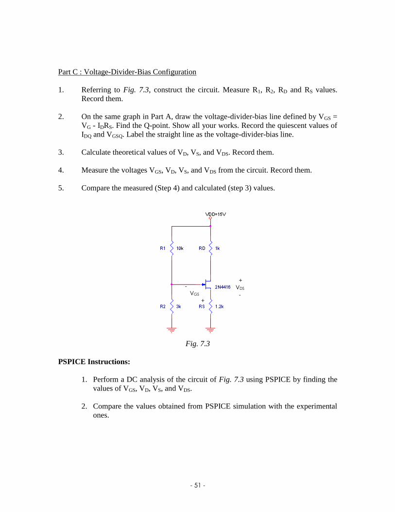
Part C : Voltage-Divider-Bias Configuration
1. Referring to Fig. 7.3, construct the circuit. Measure R1, R2, RD and RS values.
Record them.
2. On the same graph in Part A, draw the voltage-divider-bias line defined by VGS =
VG - IDRS. Find the Q-point. Show all your works. Record the quiescent values of
IDQ and VGSQ. Label the straight line as the voltage-divider-bias line.
3. Calculate theoretical values of VD, VS, and VDS. Record them.
4. Measure the voltages VGS, VD, VS, and VDS from the circuit. Record them.
5. Compare the measured (Step 4) and calculated (step 3) values.
Fig. 7.3
PSPICE Instructions:
1. Perform a DC analysis of the circuit of Fig. 7.3 using PSPICE by finding the
values of VGS, VD, VS, and VDS.
2. Compare the values obtained from PSPICE simulation with the experimental
ones.
-
VGS
+
+
VDS
-
- 52 -
Results and Calculations:
Part A
1. RD (measured) = _____________
2. VRD (measured) = ____________
D
RDD
R
VI
Since VGS = 0V, ID = IDSS =____________
3. VGS (measured) = ____________
VRD = 1mV; AAR
VI
D
RDD 01
Since ID ≈ 0A, VGS = VP = ____________
4. Sketch transfer curve using Schokley’s equation on graph paper. To draw the
curve, find for at least 4 points. Show all works below.
2
1
P
GS
DSSDV
VII
5 points for plot (calculated):
VGS = 0V, ID = IDSS = ___________
VGS = ______, ID = ____________
VGS = ______, ID = ____________
VGS = ______, ID = ____________
VGS = ______, ID = ____________
VGS = ______, ID = ____________
Note : VP < VGS < 0
5. From transfer curve in Step 4, if VGS = -1V, IDQ = ______________ (This is IDQ
calculated)
---------------------------------------------------------------------------------------------------------------------------------------------------------------------------------------------------
- 53 -
6. If VGS = -1V, VRD (measured) = _____________
D
RDD
R
VI
(This is IDQ measured)
7. Comparison of IDQ measured (Step 6) & IDQ calculated (Step 5):
Part B
1. RD (measured) = ______________, RS (measured) = ______________
2. On the same transfer curve in Part A, draw the self-bias line which is given by
SDGS RIV (To draw the line, find at least 2 points). Show all your works
below.
From the graph, IDQ (calculated) = _________, VGSQ (calculated) = __________
3. VGS (calculated) = ______________ , VD (calculated) = _________________ ,
VS (calculated) = ______________ , VDS (calculated) = _________________ ,
VG (calculated) = ______________
(Show your calculations)
---------------------------------------------------------------------------------------------------------------------------------------------------------------------------------------------------
- 54 -
4. VGS (measured) = ______________ , VD (measured) = _________________ ,
VS (measured) = ______________ , VDS (measured) = _________________ ,
VG (measured) = ______________
5. Compare the difference of measured (Step 4) and calculated (Step 3) values
using %100% xV
VVdifference
calc
calcmeas
%VGS = _____________, %VD = _________________ , %VS = ______________
%VDS = _________________ , %VG = ______________
Part C
1. R1 (measured) = ______________, R2 (measured) = ______________
RD (measured) = ______________, RS (measured) = ______________
2. On the same transfer curve in Part A, draw the voltage-divider-bias line which is
given by SDGGS RIVV where 21
2
RR
VRV DD
G
(To draw the line, find at least 2 points). Show all your works below.
---------------------------------------------------------------------------------------------------------------------------------------------------------------------------------------------------
- 55 -
From the graph, IDQ (calculated) = _________,VGSQ (calculated) = ____________
3. VD (calculated) = _________________ , VS (calculated) = ______________ ,
VDS (calculated) = _________________ ,
(Show your calculations below!)
4. VGS (measured) = ______________ , VD (measured) = _________________ ,
VS (measured) = ______________ , VDS (measured) = _________________ ,
5. Compare the difference of measured (Step 4) and calculated (Step 3) values
using %100% xV
VVdifference
calc
calcmeas
%VGS = ______________ , %VD = _________________ ,
%VS = ______________ , %VDS = _________________ ,
---------------------------------------------------------------------------------------------------------------------------------------------------------------------------------------------------
- 56 -
Objectives:
To theoretically analyse the basic op-amp circuits.
To build and test typical op-amp application circuits, such as inverting and
non-inverting amplifier
Equipment:
Instruments
DC power supply
Digital Multimeter (DMM)
Function Generator
Oscilloscope
Components
Op Amp : LM 741
Resistors: 1 k, 10 k (4), 22 k, 100 k (2),5 M
Procedure:
Part A: Inverting Amp
1. Set up the oscilloscope to show a dual trace, one for the input of the op-amp and
one for the output. Use DC input coupling. Set up the function generator to
produce a sine wave with an amplitude >0.5 V and frequency 1 kHz. Make sure
that the grounds of the function generator, oscilloscope, and prototyping board are
somehow connected.
2. Measure the values of your resistors, then using the prototyping board, wire up
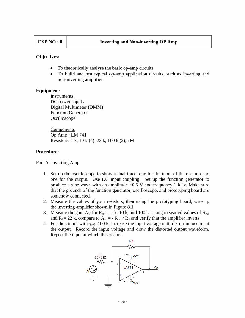
the inverting amplifier shown in Figure 8.1.
3. Measure the gain AV for Rref = 1 k, 10 k, and 100 k. Using measured values of Rref
and R1= 22 k, compare to AV = - Rref / R1 and verify that the amplifier inverts
4. For the circuit with Rref=100 k, increase the input voltage until distortion occurs at
the output. Record the input voltage and draw the distorted output waveform.
Report the input at which this occurs.
EXP NO : 8 Inverting and Non-inverting OP Amp
- 57 -
Fig. 8.1
5. For the circuit with Rref = 100 k, measure the gain AV at the logarithmically-
spaced frequencies of 100 Hz, 300 Hz, 10 kHz, ..., 1 MHz, 3 MHz. Repeat for
Rref = 10 k. Plot your results on log-log graph paper. (You will need 5 cycles for
the log paper on the frequency axis.) Also show on this graph the theoretical gain
|AV | = Rref / R1.
6. Perform the experiment to calculate the input impedance of this amplifier.
Part B: Non-Inverting Amp
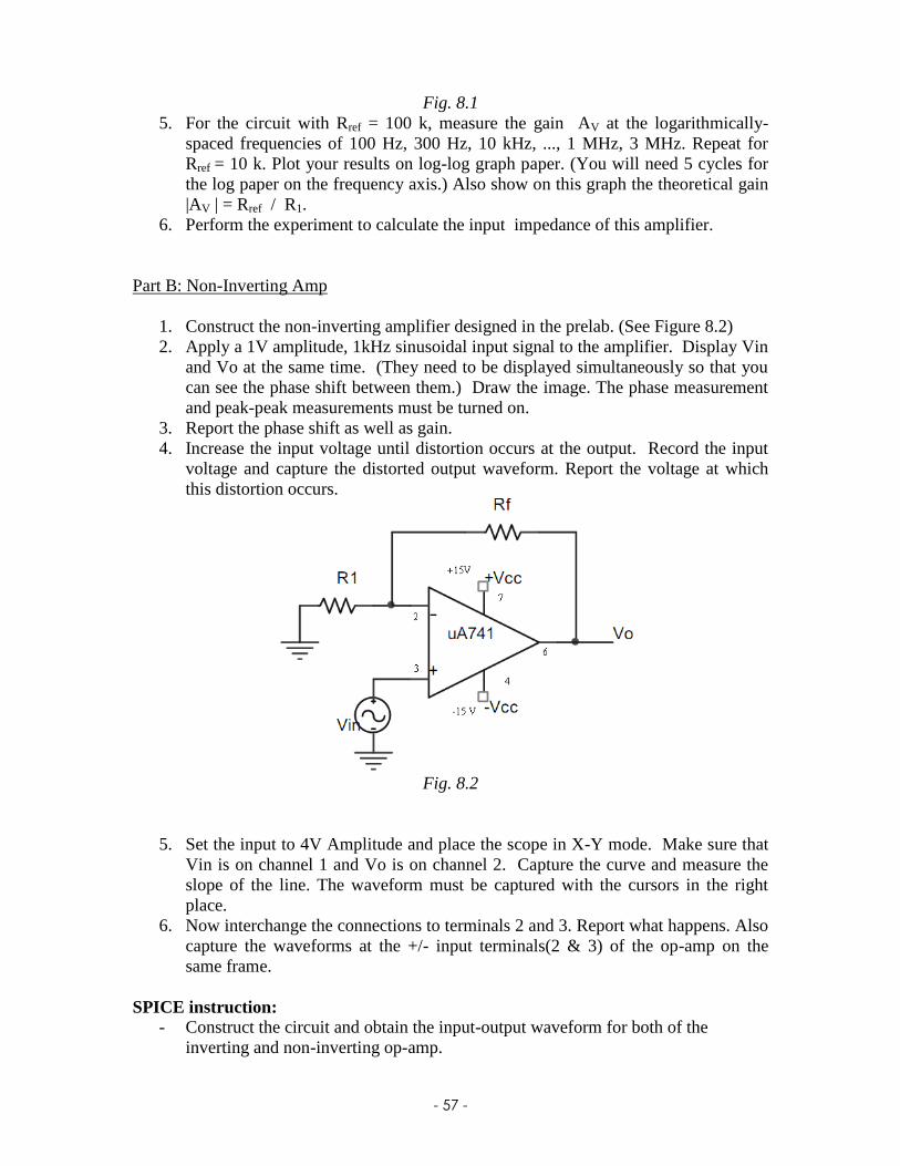
1. Construct the non-inverting amplifier designed in the prelab. (See Figure 8.2)
2. Apply a 1V amplitude, 1kHz sinusoidal input signal to the amplifier. Display Vin
and Vo at the same time. (They need to be displayed simultaneously so that you
can see the phase shift between them.) Draw the image. The phase measurement
and peak-peak measurements must be turned on.
3. Report the phase shift as well as gain.
4. Increase the input voltage until distortion occurs at the output. Record the input
voltage and capture the distorted output waveform. Report the voltage at which
this distortion occurs.
Fig. 8.2
5. Set the input to 4V Amplitude and place the scope in X-Y mode. Make sure that
Vin is on channel 1 and Vo is on channel 2. Capture the curve and measure the
slope of the line. The waveform must be captured with the cursors in the right
place.
6. Now interchange the connections to terminals 2 and 3. Report what happens. Also
capture the waveforms at the +/- input terminals(2 & 3) of the op-amp on the
same frame.
SPICE instruction:
- Construct the circuit and obtain the input-output waveform for both of the
inverting and non-inverting op-amp.
- 58 -
Results and Calculations:
Part A :
1. Vin(peak-to-peak )( measured ) = __________________
2. R1 ( measured ) = : _______________ , Rref ( measured ) =________________
3. Measure different values of Rref , to calculate Av , using Av = : - Rref/ R1
Rref =_________________________, Av =_______________________
Rref =_________________________, Av =_______________________
Rref =_________________________, Av =_______________________
4. Vin(peak-to-peak ) ( measured ) =_____________________
Draw the distorted output waveform.
5. Fill up the table measure gain Av ( Av = Vout(peak-to-peak )/ Vin(peak-to-peak ).
100Hz 300Hz 10kHz 100kHz 1MHz 3MHz
Rref =100k
Rref =10k
Plot your results on the graph paper.
The theoretical gainAv= Rref /R1 =___________________ ( calculate ).
6. The input impedance , Rin ( calculate ) =________________

- 59 -
Part B :
1. R1 ( measured ) = _________________ Rref ( measured )=______________
2. Draw the input and output signal at the same graph.
3. The output signal’s phase ,Ф ( measured)=_______________
Av (measured)= Vout(peak-to-peak) / Vin(peak-to-peak ) = _____________________
4. Vin(peak-to-peak ) ( measured ) = __________________
Vout(peak-to-peak ) ( measured ) = _________________( the voltage at which this
distortion occurs.)
Draw the distorted output waveform.
- 60 -
Objectives:
To theoretically analyse the basic op-amp circuits.
To build and test typical op-amp application circuits, such as summinb,
subtracting, integrating and differentiating amplifier
Equipment:
Instruments
DC power supply
Digital Multimeter (DMM)
Function Generator
Oscilloscope
Components
Op Amp : LM 741
Resistors: 1 k, 10 k (4), 22 k, 100 k (2),5 M
Procedure:
Summing op-amp:
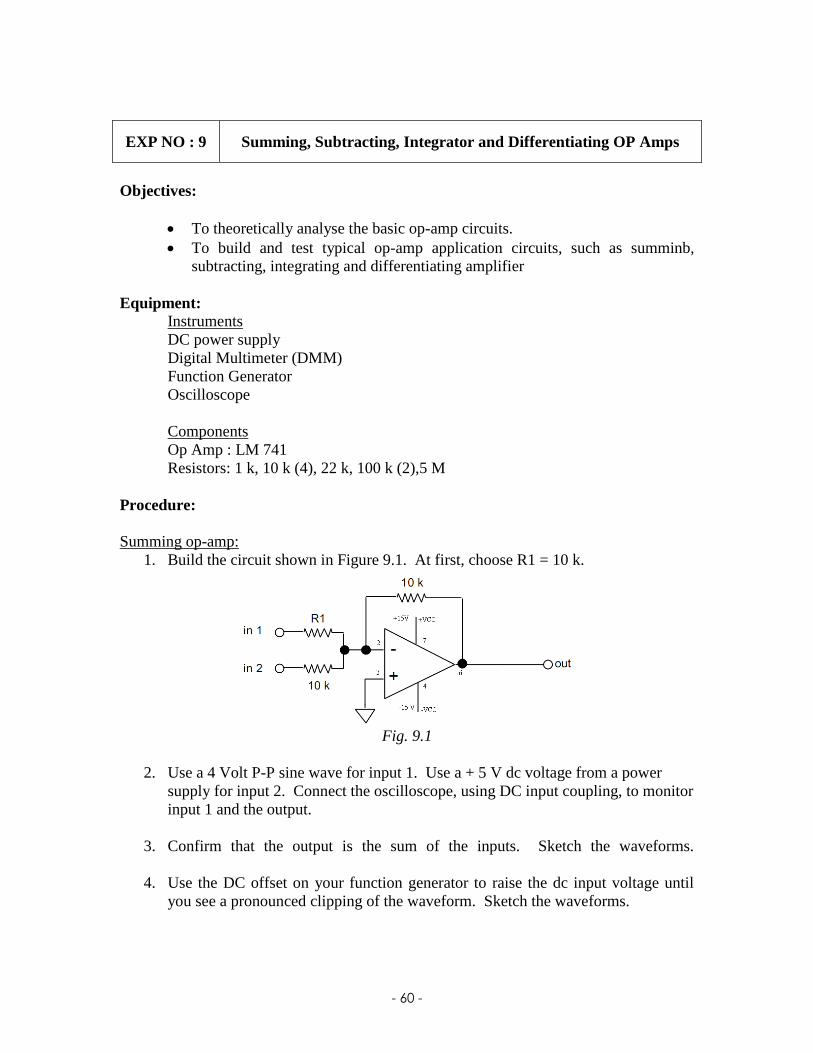
1. Build the circuit shown in Figure 9.1. At first, choose R1 = 10 k.
Fig. 9.1
2. Use a 4 Volt P-P sine wave for input 1. Use a + 5 V dc voltage from a power
supply for input 2. Connect the oscilloscope, using DC input coupling, to monitor
input 1 and the output.
3. Confirm that the output is the sum of the inputs. Sketch the waveforms.
4. Use the DC offset on your function generator to raise the dc input voltage until
you see a pronounced clipping of the waveform. Sketch the waveforms.
EXP NO : 9 Summing, Subtracting, Integrator and Differentiating OP Amps
- 61 -
Subtracting op-amp:
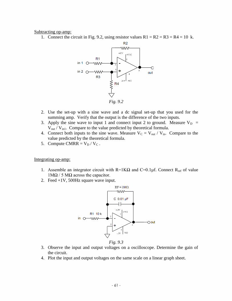
1. Connect the circuit in Fig. 9.2, using resistor values R1 = R2 = R3 = R4 = 10 k.
Fig. 9.2
2. Use the set-up with a sine wave and a dc signal set-up that you used for the
summing amp. Verify that the output is the difference of the two inputs.
3. Apply the sine wave to input 1 and connect input 2 to ground. Measure VD =
Vout / Vin1. Compare to the value predicted by theoretical formula.
4. Connect both inputs to the sine wave. Measure VC = Vout / Vin. Compare to the
value predicted by the theoretical formula.
5. Compute CMRR = VD / VC .
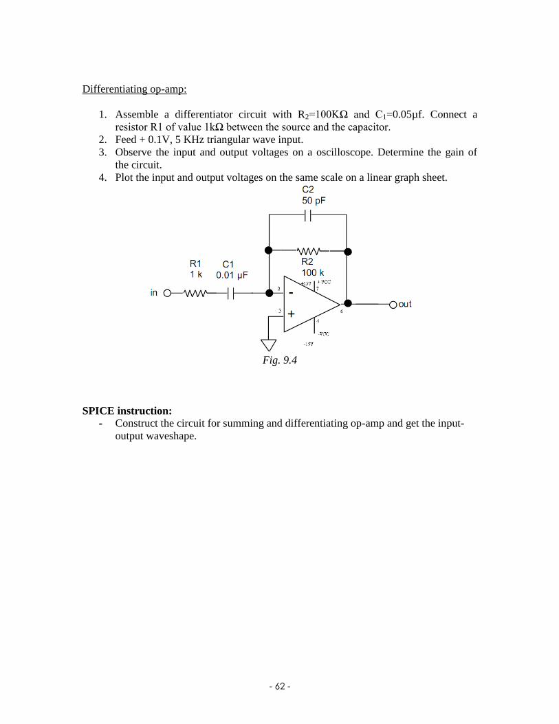
Integrating op-amp:
1. Assemble an integrator circuit with R=1KΩ and C=0.1µf. Connect Rref of value
1MΩ / 5 MΩ across the capacitor.
2. Feed +1V, 500Hz square wave input.
Fig. 9.3
3. Observe the input and output voltages on a oscilloscope. Determine the gain of
the circuit.
4. Plot the input and output voltages on the same scale on a linear graph sheet.
- 62 -
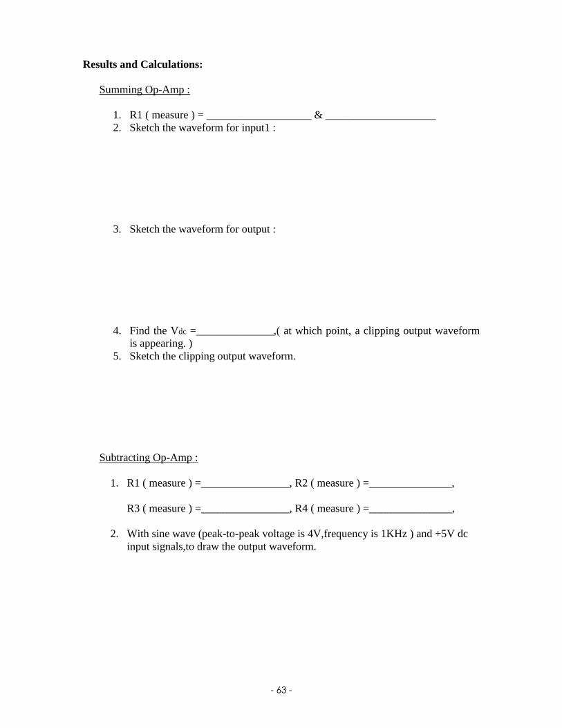
Differentiating op-amp:
1. Assemble a differentiator circuit with R2=100KΩ and C1=0.05µf. Connect a
resistor R1 of value 1kΩ between the source and the capacitor.
2. Feed + 0.1V, 5 KHz triangular wave input.
3. Observe the input and output voltages on a oscilloscope. Determine the gain of
the circuit.
4. Plot the input and output voltages on the same scale on a linear graph sheet.
Fig. 9.4
SPICE instruction: - Construct the circuit for summing and differentiating op-amp and get the input-
output waveshape.
- 63 -
Results and Calculations:
Summing Op-Amp :
1. R1 ( measure ) = ___________________ & ____________________
2. Sketch the waveform for input1 :
3. Sketch the waveform for output :
4. Find the Vdc =______________,( at which point, a clipping output waveform
is appearing. )
5. Sketch the clipping output waveform.
Subtracting Op-Amp :
1. R1 ( measure ) =________________, R2 ( measure ) =_______________,
R3 ( measure ) =________________, R4 ( measure ) =_______________,
2. With sine wave (peak-to-peak voltage is 4V,frequency is 1KHz ) and +5V dc
input signals,to draw the output waveform.

- 64 -
3. ( When in2 is connected to ground )
VD ( measure ) = Vout(pp)/Vin1(pp) =_________________
4. ( When in1 and in2 both are connected to sine wave )
VC ( measure ) = Vout(pp)/Vin1(pp) =_______________
5. CMRR ( Calculate ) = VD/VC =__________________
Integrating Op-Amp :
1. R1 ( measure ) =_______________,R2 ( measure ) =______________,
2. Vin(pp)( measure ) =_______________
Vout(pp)( measure ) =______________
3. Av = Vout(pp)/Vin(pp) =________________________( calculate )
4. Draw the waveform of output voltage and input voltage on the same scale.
Differentiating Op-Amp :
1. R1 ( measure ) =___________________, R2 ( measure ) =_________________,
2. Vin(pp)( measure ) =_________________
Vout(pp)( measure ) =________________
3. Av = Vout(pp)/Vin(pp) =_______________( calculate ).
4. Draw the waveform of output voltage and input voltage on the same scale.