en 206: power electronics and machines - inverterssuryad/lectures/en206/lecture-inverter.pdf · en...
TRANSCRIPT

EN 206: Power Electronics and MachinesInverters
Suryanarayana Doolla
Department of Energy Science and EngineeringIndian Institute of Technology Bombay
email: [email protected]
March 15, 2013
Prof. Doolla (DESE) EN 206: Inverter March 15, 2013 1 / 40

Introduction
Voltage Source Converters
The fabricated AC voltage is not affected by load
Applications:
AC Motor drives, Un interruptible power supply (UPS)Induction heating, Power conversion from PV array and fuel cellStatic Var Compensator, Static Var Generator, Active harmonic fileter
The power semi conductor devices are always forward biased due todc supply voltage.
GTO, BJT, IGCT, Power MOSFET, IGCT are suitable selfcontrolled, forward or assymetric blocking devices
Feed back diode is always connected across switch for free reverseflow of current.
Prof. Doolla (DESE) EN 206: Inverter March 15, 2013 2 / 40

Introduction
VSC - General category
Pulse Width Modulated Inverters
Input DC is essentially constantOutput voltage magnitude and frequency is controlledAchieved using Pulse Width Modulation Technique
Square Wave Inverter
Input DC is controlled to control output voltage magnitudeInverter can control only frequency of output voltageOutput voltage waveform is similar to square wave.
Single phase inverter with voltage cancellation
Input DC is essentially constantVoltage cancellation technique is applicable for single phase invertersonly.
Prof. Doolla (DESE) EN 206: Inverter March 15, 2013 3 / 40

square-wave mode of operation
Square Wave Inverter - Half bridge
Inductive load is connectedbetween point ’a’ and the centrepoint ’0’ of a split capacitorpower supply
Q1 and Q2 are closed alternatelyfor π angle to generate squarewave output voltage
Vao oscillates between +0.5Vd
and −0.5Vd
Prof. Doolla (DESE) EN 206: Inverter March 15, 2013 4 / 40

square-wave mode of operation
Single Phase inverter – Half bridge
Snubber circuit is not shown for simplicity
Short gap or lock out time td is maintained to prevent any shortcircuit or shoot-through fault due to turn-off switching delay
When supply voltage and current are of same polarity power istransferred from dc to ac or else power is fed back to source
Average power flows from source to the load
Prof. Doolla (DESE) EN 206: Inverter March 15, 2013 5 / 40

square-wave mode of operation
Single Phase Full Bridge Inverter -H Bridge
Split capacitor may not be required
Q1Q2 and Q3Q4 are operated in pairs and switched alternately togenerate square wave output voltage of amplitude Vd
Feed back current flows through D1D2 and D3D4
Both diodes are designed to withstand supply voltage Vd .
H-Bridge inverters are used in four quadrant operation
Prof. Doolla (DESE) EN 206: Inverter March 15, 2013 6 / 40

square-wave mode of operation
Voltage Control using Phase Shift
Prof. Doolla (DESE) EN 206: Inverter March 15, 2013 7 / 40

square-wave mode of operation
Voltage Control – Phase Shift
The output line voltage Vab = Va0 − Vb0 is a quasi-square wave ofpulse width “φ”, which can control the fundamental component ofoutput voltage.
Assuming a typical lagging load current with perfect filtering:Q1, Q2 conducting
Active mode with positive voltage and current
Q1, D3 conductingFree wheeling mode with positive current
D3, D4 conductingFeedback mode with positive current
Q3, Q4 conductingActive mode with negative current an negative voltage
Q4, D2 conductingFree wheeling with negative current
D1, D2 conductingFeedback mode with negative current
Prof. Doolla (DESE) EN 206: Inverter March 15, 2013 8 / 40
square-wave mode of operation
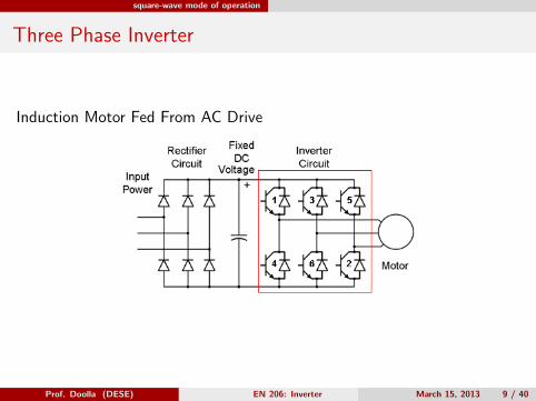
Three Phase Inverter
Induction Motor Fed From AC Drive
Prof. Doolla (DESE) EN 206: Inverter March 15, 2013 9 / 40

square-wave mode of operation
Three Phase Square Wave Inverter - Waveform
Prof. Doolla (DESE) EN 206: Inverter March 15, 2013 10 / 40

square-wave mode of operation
Three Phase Inverter - Harmonic Spectrum
Prof. Doolla (DESE) EN 206: Inverter March 15, 2013 11 / 40

square-wave mode of operation
Three Phase Inverter - Analysis
VLL,1(rms) =√
32 ×
4π ×
Vd2 = 0.78Vd
VLL does not depend on load condition and contains harmonics dueto switching.
VLL,1(rms) = 0.78Vd/h where, h = 6n ± 1
It is not possible to control output voltage by using voltagecancellation technique in three phase inverter
The period of conduction of each switch is determined by the powerfactor of the load
Harmonic Spectrum
Even and Triplen harmonics are not presentPWM switching result in small ripple current
Prof. Doolla (DESE) EN 206: Inverter March 15, 2013 12 / 40

Pulse Width Modulation
Pulse Width Modulation (PWM)
Definition:??PWM inverters are becoming more popular for control of industrialdrives advances in solid-state power devices and microprocessors.Frequency and magnitude of voltage and current of the motor can becontrolledTypes: Hysteresis PWM, Sine triangular PWM and space vectorPWM
Prof. Doolla (DESE) EN 206: Inverter March 15, 2013 13 / 40

Pulse Width Modulation
Sine Triangular PWM (SPWM)
Prof. Doolla (DESE) EN 206: Inverter March 15, 2013 14 / 40

Pulse Width Modulation
Sine Triangular PWM (SPWM)
Peak amplitude of the fundamental frequency component is ma timesVd2
The harmonics in the inverter output voltage waveform appear as sidebands, centered around the switching frequency
The harmonics are given by fh = (jmf ± k)f1
For odd values of j, the harmonics exist only for even values of k.
For even values of j, the harmonics exist only for odd values of k
Prof. Doolla (DESE) EN 206: Inverter March 15, 2013 15 / 40

Pulse Width Modulation
Single Phase SPWM - Harmonic AnalysisHarmonics of VAo for a large mf . VAo,h/
Vd
2 = VAN,h/Vd
2 is tabulated as afunction of ma.
ma 0.2 0.4 0.6 0.8 1.01 0.2 0.4 0.6 0.8 1.0mf 1.242 1.15 1.006 0.818 0.601
mf ± 2 0.016 0.061 0.131 0.220 0.318mf ± 4 0.018
2mf ± 1 0.19 0.326 0.37 0.314 0.1812mf ± 3 0.024 0.071 0.139 0.2122mf ± 5 0.013 0.033
3mf 0.335 0.123 0.083 0.171 0.1133mf ± 2 0.044 0.139 0.203 0.176 0.0623mf ± 4 0.012 0.047 0.104 0.1573mf ± 6 0.016 0.0444mf ± 1 0.163 0.157 0.008 0.105 0.0684mf ± 3 0.012 0.07 0.132 0.115 0.0094mf ± 5 0.034 0.084 0.1194mf ± 7 0.017 0.050
Prof. Doolla (DESE) EN 206: Inverter March 15, 2013 16 / 40

Pulse Width Modulation
Sine Triangular PWM (SPWM)
By choosing mf as odd integer results in odd symmetry as well as halfwave symmetry with time origin.
Only odd harmonics are present and the even harmonics disappearfrom the output waveform
Coefficients of the sine series in the fourier analysis are finite
Coefficients of the cosine series are zero
Switching losses are proportional to switching frequency Higherswitching frequency ⇒ more losses
Small value of mf ≤ 21Synchronous PWM
mf should be an integer otherwise, possibility of sub harmonics
mf should be an odd integer
Harmonics due to over modulation (ma > 2.5)
Prof. Doolla (DESE) EN 206: Inverter March 15, 2013 17 / 40

Pulse Width Modulation
SPWM - Over modulation
Prof. Doolla (DESE) EN 206: Inverter March 15, 2013 18 / 40

Pulse Width Modulation
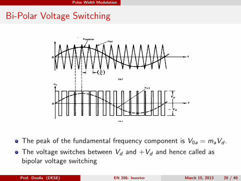
Bi-Polar Voltage Switching
CIRCUIT DIAGRAM
The diagonally opposite switches (TA+ and TB−) and (TA−, TB+)are switches as pairs.
The output of inverter leg B is negative of the leg A output.
When TA+ is ON, VA0 = +Vd2 and when TB− is ON VB0 = −Vd
2
Prof. Doolla (DESE) EN 206: Inverter March 15, 2013 19 / 40
Pulse Width Modulation
Bi-Polar Voltage Switching
The peak of the fundamental frequency component is V0a = maVd .
The voltage switches between Vd and +Vd and hence called asbipolar voltage switching
Prof. Doolla (DESE) EN 206: Inverter March 15, 2013 20 / 40

Pulse Width Modulation
Bi-Polar Voltage Switching
The lowest harmonics appear as side band of twice the switchingfrequency.
Harmonic component of switching frequency disappear
Prof. Doolla (DESE) EN 206: Inverter March 15, 2013 21 / 40

Pulse Width Modulation
Bi-Polar Voltage Switching
The output current circulates in a loop through TA+ and DB+ orDA+ and TB+ depending on the direction of i0.
The output voltage changes between zero and +Vd or zero and Vd
and hence names are unipolar voltage switching.
The voltage jumps in output is limited to Vd compared to 2Vd in thecase of bipolar scheme.
Prof. Doolla (DESE) EN 206: Inverter March 15, 2013 22 / 40

Pulse Width Modulation
Bi-Polar Voltage Switching
The switches in the two legs of the full bridge are not switchedsimultaneously
Leg A and Leg B are controlled by comparing Vtri with Vcontrol andVcontrol respectively
Prof. Doolla (DESE) EN 206: Inverter March 15, 2013 23 / 40

Pulse Width Modulation
Uni-Polar Voltage Switching
Prof. Doolla (DESE) EN 206: Inverter March 15, 2013 24 / 40

Pulse Width Modulation
Uni-Polar Voltage Switching Pattern
Control logic - Switching Pattern
Vcontrol > Vtri ; TA+ on and VAN = Vd
Vcontrol < Vtri ; TA− on and VAN = 0−Vcontrol > Vtri ; TB+ on and VBN = Vd
−Vcontrol < Vtri ; TB− on and VBN = 0
Combination of switch on states and corresponding voltages
TA+ and TB− on, VAN = Vd , VBN = 0, V0 = Vd
TA− and TB+ on, VAN = 0, VBN = Vd , V0 = −Vd
TA+ and TB+ on, VAN = Vd , VBN = Vd , V0 = 0TA− and TB− on, VAN = 0, VBN = 0, V0 = 0
When all the upper switches are on simultaneously, the outputvoltage is zero. The same is true for lower switches
Prof. Doolla (DESE) EN 206: Inverter March 15, 2013 25 / 40

Pulse Width Modulation
Three Phase SPWM - Switching Pattern
Prof. Doolla (DESE) EN 206: Inverter March 15, 2013 26 / 40

Pulse Width Modulation
Three Phase SPWM - Harmonic Analysis
Prof. Doolla (DESE) EN 206: Inverter March 15, 2013 27 / 40

Pulse Width Modulation
Three Phase SPWM - Harmonic Analysis
Harmonics of VLL for a large and odd mf that is multiple of 3.
ma 0.2 0.4 0.6 0.8 1.0
1 0.122 0.245 0.367 0.49 0.612
mf ± 2 0.010 0.037 0.080 0.135 0.195mf ± 4 0.005 0.011
2mf ± 1 0.116 0.2 0.227 0.192 0.1112mf ± 5 0.008 0.020
3mf ± 2 0.027 0.085 0.124 0.108 0.0383mf ± 4 0.007 0.029 0.064 0.096
4mf ± 1 0.1 0.096 0.005 0.064 0.0424mf ± 5 0.021 0.051 0.0734mf ± 7 0.01 0.03
Note: VLL,h/Vd are tabulated as a function of ma where VLL,h are the rmsvalues of the harmonic voltages.
Prof. Doolla (DESE) EN 206: Inverter March 15, 2013 28 / 40

Pulse Width Modulation
Triangular wave form is compared to three sinusoidal waveforms 120o
apart to generate pulses for the bridge circuit
DC voltage present in the phase voltage gets canceled out in the linevoltages
In the case of three phase inverter, only line voltages are ofimportance
The phase difference between mthf harmonic is zero between two
phases and hence cancel out in line voltage, mf is odd integer andmultiple of 3.
Dominant harmonics present in single phase inverter are eliminatedfrom the line-line voltage of a three phase inverter
The peak value of fundamental of one of the leg of inverter isV̂AN,1 = ma
Vd2 and the line-line voltage is given by
VLL,1(rms) =√
32(V̂AN,1) = 0.612maVd
Prof. Doolla (DESE) EN 206: Inverter March 15, 2013 29 / 40
Pulse Width Modulation
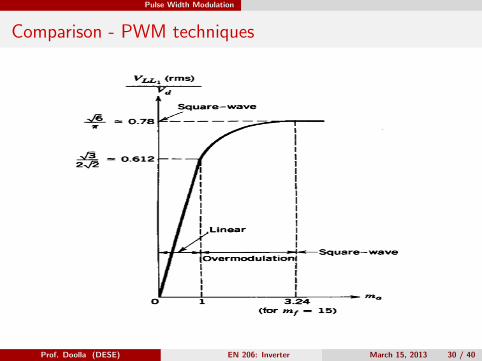
Comparison - PWM techniques
Prof. Doolla (DESE) EN 206: Inverter March 15, 2013 30 / 40

Pulse Width Modulation
Space Vector PWM
Vab
Vbc
Vca
=Vdc
1 −1 00 1 −1−1 0 1
abc
Va
Vb
Vc
=13Vdc
2 −1 −1−1 2 −1−1 −1 2
abc
When the upper switch in ON the corresponding lower switch is OFF
The state of the switch is sufficient to evaluate the output voltage
There are eight possible combinations for on/off state of the upperswitches
Prof. Doolla (DESE) EN 206: Inverter March 15, 2013 31 / 40

Pulse Width Modulation
SVPWM - On/Off state and Corresponding Output
Switch Phase LineState Voltage Voltage
0 0 0 0 0 0 0 0 01 0 0 2/3 -1/3 -1/3 1 0 -11 1 0 1/3 1/3 -2/3 0 1 -10 1 0 -1/3 2/3 -1/3 -1 1 00 1 1 -2/3 1/3 1/3 -1 0 10 0 1 -1/3 -1/3 2/3 0 -1 11 0 1 1/3 -2/3 1/3 1 -1 01 1 1 0 0 0 0 0 0
Prof. Doolla (DESE) EN 206: Inverter March 15, 2013 32 / 40

Pulse Width Modulation
Sample calculations for HexagonVa
Vb
Vc
=13Vdc
2 −1 −1−1 2 −1−1 −1 2
abc
Tabc−dq =
√23
[1 −1/2 −1/2
0√
3/2 −√
3/2
]Va
Vb
Vc
[dq
]=√
23
[1 −1/2 −1/2
0√
3/2 −√
3/2
]13Vdc
2 −1 −1−1 2 −1−1 −1 2
abc
For vector U100: Substituting a=1, b=0, c=0 gives,[
dq
]=√
23
[1 −1/2 −1/2
0√
3/2 −√
3/2
]13Vdc
2 −1 −1−1 2 −1−1 −1 2
100
[dq
]=
[√(2/3)0
]Prof. Doolla (DESE) EN 206: Inverter March 15, 2013 33 / 40

Pulse Width Modulation
SVPWM - Table for Space Vector
a b c Va Vb Vc Vab Vbc Vca
0000 0 0 0 0 0 0 0 0 0U100 1 0 0 2/3 -1/3 -1/3 1 0 -1U110 1 1 0 1/3 1/3 -2/3 0 1 -1U010 0 1 0 -1/3 2/3 -1/3 -1 1 0U011 0 1 1 -2/3 1/3 1/3 -1 0 1U001 0 0 1 -1/3 -1/3 2/3 0 -1 1U101 1 0 1 1/3 -2/3 1/3 1 -1 0U111 1 1 1 0 0 0 0 0 0
The generated or reference voltage shall lie in the hexagon formed by theabove vectors.
Prof. Doolla (DESE) EN 206: Inverter March 15, 2013 34 / 40

Pulse Width Modulation
SVPWM- Hexagon of Vectors
There are total of 6 sectors in which the reference voltage Uout shallbelong to.
If the reference output voltage magnitude and angle is given, then|Uout | and α can be computed. Where α is angle between Uout andUx .
From |Uout| and α, the sector of reference voltage Uout can be easilycomputed.
Time period for which the vectors shall operate is given by:
T1 + T2 + T0 = Tpwm
T1 =√
(2)Tpwm|Uout |cos(α + 300)T2 =
√(2)Tpwm|Uout |sin(α)
TpwmUout = T1Ux + T2U(x±60) + T0(0000or0111)
Prof. Doolla (DESE) EN 206: Inverter March 15, 2013 35 / 40

Pulse Width Modulation
SVPWM - Switching Direction
Prof. Doolla (DESE) EN 206: Inverter March 15, 2013 36 / 40

Pulse Width Modulation
SVPWM - Switching Pattern
The maximum value of Uout is the shortest radius of the envelope
The maximum rms value of line-line voltage is Vd√2
and the maximum
rms value of phase voltage is Vd√6
which is 2√3
times higher than that
of sine triangular PWM technique
If the motor is rated for Vrms (three phase L-L) then the dc busrequires shall be Vd =
√2× Vrms
Ux can be basic closest space vector on either side of Uout .Ux+60(orUx−60) is basic space vector on the opposite side
Prof. Doolla (DESE) EN 206: Inverter March 15, 2013 37 / 40

Pulse Width Modulation
SVPWM - Switching
T1 represents component on Ux and T2 represent component on theother vector Each PWM channel switches twice per every PWMperiod except when the duty cycle is 0% or 100%.
There is a fixed switching order among the three PWM channels foreach sector
Every PWM period starts and ends with O000; The amount of O000
inserted is the same as that of O111 in each PWM period
The above is applicable for symmetric PWM
Prof. Doolla (DESE) EN 206: Inverter March 15, 2013 38 / 40

Pulse Width Modulation
Three Phase SPWM - Switching Pattern
Prof. Doolla (DESE) EN 206: Inverter March 15, 2013 39 / 40

Pulse Width Modulation
Three Phase SPWM - Inverter Output
Prof. Doolla (DESE) EN 206: Inverter March 15, 2013 40 / 40