emulation of microprocessor memory systems using …krste/papers/aik-sm.pdf · with the computer...
TRANSCRIPT

Emulation of Microprocessor Memory Systems
Using the RAMP Design Framework
by
Asif I. Khan
Submitted to the Department of Electrical Engineering and ComputerScience
in partial fulfillment of the requirements for the degree of
Master of Science in Electrical Engineering and Computer Science
at the
MASSACHUSETTS INSTITUTE OF TECHNOLOGY
February 2008
c© Massachusetts Institute of Technology 2008. All rights reserved.
Author . . . . . . . . . . . . . . . . . . . . . . . . . . . . . . . . . . . . . . . . . . . . . . . . . . . . . . . . . . . . . .Department of Electrical Engineering and Computer Science
Feb 1, 2008
Certified by. . . . . . . . . . . . . . . . . . . . . . . . . . . . . . . . . . . . . . . . . . . . . . . . . . . . . . . . . .Krste Asanovic
Associate ProfessorThesis Supervisor
Accepted by . . . . . . . . . . . . . . . . . . . . . . . . . . . . . . . . . . . . . . . . . . . . . . . . . . . . . . . . .Terry P. Orlando
Chairman, Department Committee on Graduate Students
Emulation of Microprocessor Memory Systems Using the
RAMP Design Framework
by
Asif I. Khan
Submitted to the Department of Electrical Engineering and Computer Scienceon Feb 1, 2008, in partial fulfillment of the
requirements for the degree ofMaster of Science in Electrical Engineering and Computer Science
Abstract
With the computer hardware industry and the academic world focused on multi-processor systems, the RAMP project is aiming to provide the infrastructure forsupporting high-speed emulation of large scale, massively-parallel multiprocessor sys-tems using FPGAs. The RAMP design framework provides the platform for buildingthis infrastructure. This research utilizes this design framework to emulate variousmicroprocessor memory systems through a model built in an FPGA.
We model both the latency and the bandwidth of memory systems through aparameterized emulation platform, thereby, demonstrating the validity of the designframework. We also show the efficiency of the framework through an evaluation ofthe utilized FPGA resources.
Thesis Supervisor: Krste AsanovicTitle: Associate Professor
2

Acknowledgments
First and foremost, I would like to thank Krste for being a dedicated advisor and
an inspiring teacher. It was his encouragement and patience that made this thesis
possible.
I would also like to thank Arvind for believing in me and for supporting me in the
past two years.
All the members of the SCALE group and the CSG-Arvind group have been a
great source of advice and support, and I would like to thank them for it.
I would also like to thank my family for their love and encouragement, and my
wife for her love and patience.
In the end, a very special thanks to Prof. Terry Orlando for seeing me through
some very tough times.
3

Contents
1 Introduction 8
1.1 Related Research . . . . . . . . . . . . . . . . . . . . . . . . . . . . . 9
1.2 Thesis Outline . . . . . . . . . . . . . . . . . . . . . . . . . . . . . . . 9
2 RAMP Design Framework 11
2.1 RAMP Target Model . . . . . . . . . . . . . . . . . . . . . . . . . . . 12
2.2 RAMP Channel Model . . . . . . . . . . . . . . . . . . . . . . . . . . 14
2.3 RAMP Host Model . . . . . . . . . . . . . . . . . . . . . . . . . . . . 16
2.3.1 Wrappers . . . . . . . . . . . . . . . . . . . . . . . . . . . . . 16
2.3.2 Links . . . . . . . . . . . . . . . . . . . . . . . . . . . . . . . . 17
2.3.3 Engine . . . . . . . . . . . . . . . . . . . . . . . . . . . . . . . 17
3 Emulation Platform 18
3.1 Processor Unit . . . . . . . . . . . . . . . . . . . . . . . . . . . . . . 18
3.1.1 SMIPS Processor . . . . . . . . . . . . . . . . . . . . . . . . . 18
3.1.2 Data-side and Instruction-side Caches . . . . . . . . . . . . . . 23
3.1.3 Memory Arbiter . . . . . . . . . . . . . . . . . . . . . . . . . . 24
3.2 Processor Wrapper . . . . . . . . . . . . . . . . . . . . . . . . . . . . 24
3.3 Memory Unit . . . . . . . . . . . . . . . . . . . . . . . . . . . . . . . 24
3.3.1 Memory Controller . . . . . . . . . . . . . . . . . . . . . . . . 25
3.3.2 Physical Memory . . . . . . . . . . . . . . . . . . . . . . . . . 26
3.4 Memory Wrapper . . . . . . . . . . . . . . . . . . . . . . . . . . . . . 26
3.5 Channel . . . . . . . . . . . . . . . . . . . . . . . . . . . . . . . . . . 27
4

3.6 Physical Link . . . . . . . . . . . . . . . . . . . . . . . . . . . . . . . 28
4 Implementation on Host 29
4.1 BEE2 . . . . . . . . . . . . . . . . . . . . . . . . . . . . . . . . . . . 29
4.2 Host Model . . . . . . . . . . . . . . . . . . . . . . . . . . . . . . . . 29
4.3 Operation of the Emulation Platform . . . . . . . . . . . . . . . . . . 31
4.3.1 Read Requests and Responses . . . . . . . . . . . . . . . . . . 32
4.3.2 Write Requests and Responses . . . . . . . . . . . . . . . . . . 33
5 Analysis and Evaluation 35
5.1 Experimental Methodology . . . . . . . . . . . . . . . . . . . . . . . . 35
5.2 Performance Evaluation . . . . . . . . . . . . . . . . . . . . . . . . . 36
5.3 Analysis of Resource Utilization . . . . . . . . . . . . . . . . . . . . . 43
6 Conclusion 46
A SMIPS Instruction Set 47
Bibliography 49
5

List of Figures
2-1 RAMP Target Model . . . . . . . . . . . . . . . . . . . . . . . . . . . 12
2-2 RAMP Target Unit Interface . . . . . . . . . . . . . . . . . . . . . . . 13
2-3 Message Fragmentation . . . . . . . . . . . . . . . . . . . . . . . . . . 15
2-4 RAMP Target Channel . . . . . . . . . . . . . . . . . . . . . . . . . . 16
3-1 Emulation Platform . . . . . . . . . . . . . . . . . . . . . . . . . . . . 19
3-2 SMIPS Processor . . . . . . . . . . . . . . . . . . . . . . . . . . . . . 20
3-3 Memory Controller Interface . . . . . . . . . . . . . . . . . . . . . . . 26
4-1 Host Model . . . . . . . . . . . . . . . . . . . . . . . . . . . . . . . . 30
5-1 IPC count for median . . . . . . . . . . . . . . . . . . . . . . . . . . . 37
5-2 IPC count for multiply . . . . . . . . . . . . . . . . . . . . . . . . . . 38
5-3 IPC count for qsort . . . . . . . . . . . . . . . . . . . . . . . . . . . . 38
5-4 IPC count for towers . . . . . . . . . . . . . . . . . . . . . . . . . . . 39
5-5 IPC count for vvadd . . . . . . . . . . . . . . . . . . . . . . . . . . . 39
5-6 Memory Latency for median . . . . . . . . . . . . . . . . . . . . . . . 40
5-7 Memory Latency for multiply . . . . . . . . . . . . . . . . . . . . . . 41
5-8 Memory Latency for qsort . . . . . . . . . . . . . . . . . . . . . . . . 41
5-9 Memory Latency for towers . . . . . . . . . . . . . . . . . . . . . . . 42
5-10 Memory Latency for vvadd . . . . . . . . . . . . . . . . . . . . . . . . 42
6

List of Tables
3.1 Branch Prediction — Possible Scenarios . . . . . . . . . . . . . . . . 22
3.2 Address Fields . . . . . . . . . . . . . . . . . . . . . . . . . . . . . . . 23
3.3 Memory Wrapper Parameters . . . . . . . . . . . . . . . . . . . . . . 27
4.1 Parameter Values for the Example Implementation . . . . . . . . . . 32
4.2 Read Requests and Responses . . . . . . . . . . . . . . . . . . . . . . 32
4.3 Write Requests and Responses . . . . . . . . . . . . . . . . . . . . . . 33
5.1 Modeled Configurations with Parameters . . . . . . . . . . . . . . . . 35
5.2 Modeled Memory Systems . . . . . . . . . . . . . . . . . . . . . . . . 36
5.3 Total Resources Utilized in Configuration A . . . . . . . . . . . . . . 43
5.4 Total Resources Utilized in Configuration B . . . . . . . . . . . . . . 44
5.5 Total Resources Utilized in Configuration C . . . . . . . . . . . . . . 44
5.6 Total Resources Utilized in Configuration D . . . . . . . . . . . . . . 44
5.7 Total Resources Utilized in Configuration E . . . . . . . . . . . . . . 45
7

Chapter 1
Introduction
To continue improving system performance both the computer hardware industry
and the academic world shifted its focus from high speed single core systems to
massively-parallel multi-core systems. The RAMP (Research Accelerator for Multi-
processors) project was initiated with an aim to develop infrastructure for supporting
high-speed emulation of large scale, massively-parallel multiprocessor systems us-
ing Field-Programmable Gate Arrays (FPGA) platforms, thereby, enabling research
on multicore operating systems, compilers, programming languages and scientific li-
braries as well as hardware multiprocessor systems to be carried out [1].
FPGAs became the platform of choice for the following reasons.
• They provide a very rapid turnaround for new hardware designs.
• They provide operating speeds of 100 to 200 MHz which are slower than real
hardware but are orders of magnitude faster than those of software simulators.
• Exploiting Moore’s Law, their density is growing at about the same rate as the
number of cores per microprocessor die.
• They are cheap and have low power consumption.
In order to meet the goals of the RAMP project a standardized design framework
called the RAMP design framework (RDF) [1, 2] was developed. In this thesis we use
this framework to to emulate various microprocessor memory systems through a model
8

built in an FPGA. We model both the latency and the bandwidth of memory systems
through a parameterized emulation platform, thereby, demonstrating the validity of
the design framework. We also show the efficiency of the framework through an
evaluation of the utilized FPGA resources.
1.1 Related Research
FPGA-based emulation platforms for parallel systems date back to the RPM project [3].
With the computer hardware Industry and the academic world focused on multicore
systems and the increasing FPGA densities, there is a renewed interest for such sys-
tems. FAST [4] is an FPGA-based framework for modeling chip multiprocessors
(CMPs) with MIPS cores, and ATLAS [5] is the first prototype for CMPs with hard-
ware support for transactional memory.
Research efforts have also focused on using the FPGAs to accelerate simulators [6,
7, 8]. Hong et al. have used FPGAs in a working system to quickly simulate various
configurations of lower level caches [9]. Finally, there have been efforts to map large
out-of-order processors using FPGAs as a prototyping medium [10].
1.2 Thesis Outline
Chapter 2 describes the RAMP design framework in detail. We begin by defining
the RAMP target model where we provide the details of the RAMP unit. We then
define the notion of time in the RAMP target model. We also provide the details
of the RAMP channel model. We conclude the chapter with a description of the
components of the RAMP host model.
Chapter 3 provides a description of the emulation platform while chapter 4 pro-
vides the details of the host model. We describe all the components of the emulation
platform in detail and provide an example implementation of the host model.
In chapter 5 we configure the emulation platform with five different sets of pa-
rameters. Using these parameter sets, we model both the latency and the bandwidth
9

of memory systems. We then analyze the performance of the platform using SMIPS
benchmarks. We also provide the details of the resources utilized by the host model.
The thesis concludes with chapter 6, which provides a summary of the research.
10

Chapter 2
RAMP Design Framework1
In order to enable high-performance simulation and emulation of large scale, massively
parallel systems on a wide variety of implementation platforms and to enable a large
community of users to cooperate and build a useful library of inter-operable hardware
models, a standardized framework, called the RAMP design framework (RDF), was
developed [1, 2]. The design framework has a number of challenging goals.
• The framework must support both cycle-accurate emulations of detailed param-
eterized machine models and rapid functional-only emulations.
• The framework should also hide changes in the underlying RAMP implemen-
tation from the designer as much as possible, to allow groups with different
hardware and software configurations to share designs, reuse components and
validate experimental results.
• In addition, the framework should not dictate the implementation language
chosen by the developers.
In RDF the design of interest, e.g. the one being emulated, is referred to as the
target, whereas the machine performing the emulation is referred to as the host.
1The RAMP design framework description presented in this chapter is a condensed version of aprevious publication [2]. It is included here for completeness.
11
2.1 RAMP Target Model
A RAMP target model [2] is a collection of loosely coupled units communicating
using latency-insensitive protocols implemented by sending messages over well-defined
channels. In practice, a unit will typically be a relatively large component, consisting
of tens of thousands of gates in a hardware implementation, e.g. a processor with L1
cache, a memory controller or a network controller. All communication between units
is via messages sent over unidirectional point-to-point inter-unit channels, where each
channel is buffered to allow the units to execute decoupled from each other.
Figure 2-1: RAMP Target Model
RAMP is designed to support a wide range of accuracy with respect to timing,
from cycle accurate simulations to purely functional emulations. Purely functional
emulations of course represent the simple case, where no measurement of time is
required, and any which exist are incidental. However, because a RAMP simulation
may require cycle accurate results, an implementation must maintain a strict notion
of time with respect to the target system. Thus the term target cycle is introduced
to describe a unit of time in the target system [2].
In order to take into account semi-synchronous systems a unit is defined as a single
clock domain. This means that the target clock rate of a unit is the rate at which
it runs relative to the target design. For example, the CPUs will usually have the
highest target clock rate and all the other units will have some rational divisor of the
12

target CPU clock rate. This implies that two units at each end of a channel can have
different target clock rates, further complicating cycle accurate simulation.
Two units at each end of a channel are only synchronized via the point-to-point
channels. The basic principle followed is that a unit cannot advance by a target
clock cycle until it has received a target clock cycle’s worth of activity on each input
channel and the output channels are ready to receive another target cycle’s worth
of activity. This scheme forms a distributed concurrent event simulator, where the
buffering in the channels allows units to run at varying target and host rates while
remaining logically synchronized in terms of target clock cycles.
It should be noted that time in the target system is purely virtual, and thus
is not tightly coupled to either the real time or the host system’s notion of time.
The primary goal of the RAMP Design Framework is to support research through
system emulation, not to build production computing systems. This distinction is
particularly important for hardware (FPGA) host implementations: the goal is not
to build computers from FPGAs.
Figure 2-2: RAMP Target Unit Interface
13

Figure 2-2 shows a schematic of the interfaces of the RAMP target unit [2]. Each
port has a FIFO-style interface which provides a natural match to the channel se-
mantics. Input messages are consumed by asserting the appropriate X READ when
the associated X READY is asserted. Similarly output messages are produced by as-
serting X WRITE, when the associated X READY is asserted. Each port is also given a
message size or bitwidth. In addition to the ports, there are two connections, Start
and Done, which are used to trigger the unit to perform one target cycle worth of
action.
2.2 RAMP Channel Model
The key to inter-unit communication, as well as many of the fundamental goals of
the RAMP project, lies in the channel model.
The target channel model [2] is lossless, strictly typed, point-to-point, and unidi-
rectional with ordered delivery. This should be intuitively viewed as being similar to
a FIFO or a circular queue with single input and output, which carries strictly typed
messages.
Channels are strictly typed with respect to the messages they can convey. A
message in RAMP is the unit of data which a channel carries between units, however,
this does not in any way restrict the use or movement of data within a unit. In
keeping with the flexibility goal of RAMP, and to expand its utility as a performance
simulation platform, the concept of a message fragment is introduced. It is the unit
of data which a channel carries during one target cycle. Figure 2-3 illustrates the
difference between a message and a message fragment.
Fragments provide RAMP with a great deal of flexibility in the performance of
channels. Fragmentation allows RAMP to decouple the size of messages, which is
a characteristic of a unit port, from the size of data moving through the channels.
This allows channels to be parameterized with respect to key performance parameters
without sacrificing interoperability.
There are three primary variables associated with every channel: bitwidth, latency
14

Figure 2-3: Message Fragmentation
and buffering. Of course to be useful a channel must have a minimum bitwidth of 1.
However in order to ensure that the RAMP architecture can be feasibly implemented
and maintain a complete decoupling between units, both the latency and buffering
must be at least 1.
The minimum latency of 1 simply states that the receiving unit cannot receive
a message in the same cycle that the sender sends it in. This is required in order
to ensure that all messages may be presented to a unit at the beginning of a target
cycle, while it may send a message at any point during the target cycle.
The minimum buffering requirement of 1 exists so that two units connected by a
channel may not have a control dependency of zero cycles. This is because without
this minimum buffering the sending unit’s ability to send a message in a certain cycle
will depend directly on whether or not the receiver receives a messages in that same
cycle.
With these two minimum requirements, a natural and efficient implementation of
the handshaking is a credit based flow control as shown in figure 2-4.
The benefit of enforcing a standard channel-based communication strategy be-
tween units is that many features can be provided automatically. Users can vary the
latency, bandwidth and buffering on each channel at configuration time.
15

creditcount
Send
ing
Uni
t Receiving U
nitLatency
dataBuffering
rdy deq
enqrdy
data
Bitw
idth
++
– –
cred
itFigure 2-4: RAMP Target Channel
2.3 RAMP Host Model
The RAMP host model [2] is composed of the following constructs.
2.3.1 Wrappers
Wrappers encapsulate units and provide the functionality described below.
• Multiplexing of messages down to fragments. In fact, the wrapper is also re-
sponsible for converting from whatever data representation is supported by the
target level, to whatever representation is required to actually transport data
over links.
• Demultiplexing of fragments to messages.
• Target cycle firing. This includes the logic used for determining when a target
cycle may begin based on incoming fragments.
• Enforcement of channel semantics. This includes ensuring that no more than
one message is read or written through each port on a given target cycle. It also
includes ensuring that message transmission and reception is atomic, despite the
fact that message delivery, because of fragmentation, is not.
16

2.3.2 Links
Links are the host level analog of channels. Unlike channels though, RDF imposes
almost no restrictions on links other than their ability to support the channel model
described earlier. Examples of links include direct hardware implementation of reg-
isters and FIFOs and software circular buffers.
2.3.3 Engine
In addition to wrappers and links, most implementations of a RAMP design will
require some way to drive them, e.g. a clock in hardware or a scheduler in software.
The exact job of an engine is to decide when and which wrappers are allowed to run,
often in conjunction with the wrappers themselves.
17

Chapter 3
Emulation Platform
The goal of this research was to build a platform for emulating various microprocessor
memory systems using the design framework described in chapter 2. Figure 3-1 is
a schematic that shows the emulation platform. This chapter describes the various
components of this platform in detail.
3.1 Processor Unit
The components of the processor unit and their functionality are outlined below.
3.1.1 SMIPS Processor
SMIPS is a version of the MIPS instruction set architecture (ISA), and it stands for
Simple MIPS, since it is actually a subset of the full MIPS ISA. It has the following
features.
• It includes all of the simple arithmetic instructions except for those which throw
overflow exceptions. It does not include multiply or divide instructions.
• It only supports word loads and stores.
• All jumps and branches are supported.
• It does not support interrupts, and most of the system co-processor instructions.
18

Mem
ory
Wra
pper
mem
_lat
_1m
em_l
at_2
Proc
esso
rU
nit
Mem
ory
Uni
tcr
edit
coun
t
Late
ncy
data
Buf
ferin
g
rdy
deq
enq
rdy
data
Bitwidth
++––
credit
Pro
cess
or W
rapp
er
cred
itco
unt
Late
ncy
data
Buf
ferin
g
rdy
deq
enq
rdy
data
Bitwidth
++––
credit
Figure 3-1: Emulation Platform
19
For a complete listing of the SMIPS instruction set, please refer to Appendix A.
pc
epoch
ExecuteFetch Writeback
Register FileBTB
pcQ wbQ
instReqQ dataRespQdataReqQ
instRespQ
Figure 3-2: SMIPS Processor
Figure 3-2 shows the SMIPS Processor. It is a 3-stage pipeline and implements the
above-described subset of the MIPS ISA. It also includes an 8-entry Branch Target
Buffer (BTB) for predicting branch instructions. It is connected to the instruction-
side and data-side caches by instruction request and response queues and data request
and response queues, respectively.
The processor was developed as an assignment in course 6.375: Complex Digital
Systems. It was coded in Bluespec [11].
3.1.1.1 Operation
The Fetch stage generates the next instruction address using the pc register, and sends
it to the instReqQ FIFO. It also writes the current pc+4 to the pcQ FIFO for use in
branch instructions. The response from the instruction-side cache is placed into the
instRespQ FIFO. Then the Execute stage takes the response out of the FIFO, reads
20
the register file, and performs the required operation. The result of the execution is
placed into the wbQ FIFO. If the instruction is a load or a store, a memory request
is placed into the dataReqQ FIFO. The Writeback stage is responsible for taking the
final result from the wbQ FIFO and the dataRespQ FIFO, and actually updating the
register file.
The processor correctly detects dependencies — in this case only the read-after-
write (RAW) hazards — and stalls the pipeline when these dependencies occur. De-
pendency checking is achieved by implementing the wbQ FIFO as a searchable FIFO
with two find methods. There are two find methods because an instruction can have
a maximum of two source operands.
In order to handle mispredicted branches we use a register called the epoch. An
epoch is a conceptual grouping of all instructions in between branch mispredictions.
The Fetch stage sends the epoch as the tag for all load requests. When a mispredict
occurs we clear all the queues which are holding the instructions issued after the
branch instruction, and increment the epoch. Then the Execute stage discards all
responses from the wrong epoch.
All the FIFOs are sized appropriately and have good scheduling properties for
achieving high throughput. In case of a hit, both the caches have a read/write latency
of 1 cycle, hence, the maximum achievable instruction per cycle (IPC) count is 0.5.
3.1.1.2 Branch Prediction
In order to improve performance we implemented a simple direct-mapped branch-
target-buffer (BTB). We predict only branch instructions. The predictor contains an
eight-entry table where each entry in the table is a <pc+4,target> pair. There is a
valid bits associated with each entry so that we can correctly handle the uninitialized
entries.
In the Fetch stage, the predictor uses the low order bits of pc+4 to index into
the table. We use pc+4 instead of pc because it makes the pipelining simpler. The
predictor reads out the corresponding <pc+4,target> pair from the table, and if
the pc’s match then it is declared a hit. The predicted target then gets clocked into
21

the pc register on the next cycle. If the pc’s do not match, then it is declared a miss
and we use pc+4 as the next pc. Our simple predictor uses the following invariant: If
a pc is in the table then we always predict taken, but if a pc is not in the table then
we always predict not-taken. Entries are never removed from the table they are only
overwritten. Since we are not predicting jump instructions, we know that the target
address is always correct even if our taken/not-taken prediction is incorrect. Hence,
we do not need to verify the target address, only the taken/not-taken prediction.
We pipeline the predictor hit/miss signal to the Execute stage. Because of the
invariant mentioned above, this hit/miss bit also tells us if the branch was predicted
taken or not-taken. In the Execute stage, the predictor compares the predicted
taken/non-taken bit to the calculated taken/not-taken bit. This is how the pre-
dictor determines if there as a misprediction. Four possible scenarios may arise for
the predictor, they are depicted in table 3.1.
Predicted Actual Mispredict? Action Taken
taken taken no No action
not taken taken yesKill the instruction in Fetch stage, update
the BTB, pc:=branch or jump target
taken not taken yesKill the instruction in Fetch stage, do not
update the BTB, pc:= correct pc+4
not taken not taken no No action
Table 3.1: Branch Prediction — Possible Scenarios
If the branch was predicted not-taken, but it should actually be taken, we update
the table by adding the appropriate pc+4 and branch target. If the branch was
predicted taken and it was actually not-taken, then we do not update the table. We
can invalidate the appropriate entry in the table, but to keep things simplified we
just leave the table unchanged.
22

3.1.2 Data-side and Instruction-side Caches
The instruction-side cache supports only read requests but the data-side cache sup-
ports both read and write requests. Other features of both the caches are similar and
are outlined below.
Both the caches are direct-mapped and follow writeback and write-allocate poli-
cies. They are both blocking caches, hence, there can be only one outstanding read
or write request at a time. They are composed of two arrays: data array and tag
array. Both the arrays have 512 lines, however, each line in the data array is 128-bit
long, while each line in the tag array is 20-bit long. This particular configuration is
chosen to optimize the implementation of the caches in FPGAs. Table 3.2 provides
the breakdown of the 32-bit address.
Field Bit Index
Byte offset 1:0
Word offset 3:2
Index 12:4
Tag 31:13
Table 3.2: Address Fields
On receiving a read/write request from the SMIPS processor, the cache searches
its tag array using the index bits of the address. If the tag array entry is valid and
the tag bits of the address match the tag array entry, it is declared a hit. The cache,
in case of a read request, then returns the data to the processor, or in case of a write
request, updates the entry in the data array. The caches have a read and write latency
of 1 cycle for cache hits.
If neither the tag array entry is valid nor the tag bits of the address match the
tag array entry, the cache sends a read request to the main memory. On receiving
the response from memory, the cache performs the required operation.
If the tag array entry is valid but the tag bits of the address do not match the
tag array entry, the cache first writes the 128-bit data array entry back to the main
memory and then sends a read request to the main memory. On receiving the data
23

from memory, the cache performs the required operation. This situation can only
arise in the data-side cache.
There can be two outstanding requests (a write request followed by a read request)
to the memory from the data-side cache, but there can be only one outstanding read
request from the instruction-side cache.
3.1.3 Memory Arbiter
The memory arbiter is a fair round-robin scheduler. It arbitrates between the instruction-
side cache and the data-side cache requests, and directs them to the memory unit.
On receiving responses from the memory unit it appropriately directs them to the
caches.
3.2 Processor Wrapper
The wrapper has two main functions. If required, it breaks down the 128-bit request
from the processor unit into smaller fragments and sends them to the memory unit,
and it combines the fragments from the memory unit into a 128-bit response and
forwards it to the processor unit. The size of the fragments can be specified through
the Bitwidth parameter.
It also handles target cycle firing of the processor unit using the Start and Done
signals. In our target model, the target clock frequency for the processor unit is the
same as its host frequency, so there is no need to maintain any state for Start and
Done signaling.
3.3 Memory Unit
The components of the memory unit are outlined below.
24

3.3.1 Memory Controller
Two separate memory controllers were used in this thesis. One, that I had developed
earlier, was coded in Verilog and was used for simulating the target model using Syn-
opsys VCS. The other was obtained from the University of California, Berkeley, and
was used for emulating the target model in an FPGA. Following is a brief description
of these memory controllers.
The memory controller is responsible for all of the low-level DRAM management
data transfer tasks. The tasks performed by the controller include the following.
• Reset, initialization, and clock generation
• Automatic refresh
• Issuing of Read and write command
• Automatic bank management
The memory controller is divided into three main stages. In the the first stage,
which is the Bank Request stage, we accept and buffer memory access requests until
they are ready to be processed by the corresponding Bank Command Translator.
The next stage is the Command Translate stage which translates the memory
access requests into DDR2 DRAM commands. It generates commands from all of the
Bank Command Translators and the Master Translator, and verifies them against
timing constraints. It then selects one command and forwards it to the Issue stage.
It also determines the new timing constraints based on the command it forwards.
The last stage is the Issue stage which is a simple pipeline that issues commands
onto the DDR2 DRAM command bus, and reads and writes data when required.
The controller allows access to ECC storage bits, but does not actually implement
ECC. It presents a FIFO-style interface [12] to the user as shown in figure 3-3.
The memory controller only sends read responses; no responses are given for write
requests.
25
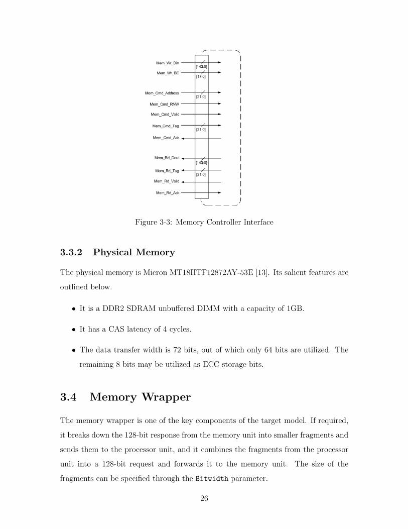
Figure 3-3: Memory Controller Interface
3.3.2 Physical Memory
The physical memory is Micron MT18HTF12872AY-53E [13]. Its salient features are
outlined below.
• It is a DDR2 SDRAM unbuffered DIMM with a capacity of 1GB.
• It has a CAS latency of 4 cycles.
• The data transfer width is 72 bits, out of which only 64 bits are utilized. The
remaining 8 bits may be utilized as ECC storage bits.
3.4 Memory Wrapper
The memory wrapper is one of the key components of the target model. If required,
it breaks down the 128-bit response from the memory unit into smaller fragments and
sends them to the processor unit, and it combines the fragments from the processor
unit into a 128-bit request and forwards it to the memory unit. The size of the
fragments can be specified through the Bitwidth parameter.
26

It also handles target cycle firing of the memory unit using the Start and Done
signals. The target clock frequency for the memory unit can be specified in terms of
the target clock frequency of the processor unit using the two parameters described
in table 3.3.
Parameter Description
mem lat 1number of cycles required by the first read/write
request fragment of a 128-bit processor request
mem lat 2number of cycles required by the subsequent
read/write request fragments of a 128-bit processor request
Table 3.3: Memory Wrapper Parameters
For simplicity, read and write requests are assumed to have the same access la-
tency. It is also assumed that the first request fragment accesses a new page in the
main memory and has a longer latency. The subsequent request fragments of a 128-bit
processor request access the same page and have a shorter latency.
The memory wrapper maintains a counter and uses time stamping for Start and
Done signaling.
3.5 Channel
The channel is the other key component in the target model. It is capable of configur-
ing the physical link in terms of bitwidth, latency and buffering. It uses credit based
flow control to implement handshaking between the processor unit and the memory
unit.
The channel and the memory wrapper work together to handle the uncertainties
in the memory unit, such as delays due to refresh. Together they are capable of
handling multiple requests in flight and block the processor unit from making more
requests when the uncertainties in the memory unit arise.
27

3.6 Physical Link
There exists a 128-bit physical link to and from the memory unit. The link is in the
form of an asynchronous FIFO because the host clock frequency for the memory unit
is much higher than the host clock frequency of the processor unit.
28

Chapter 4
Implementation on Host
4.1 BEE2
The Berkeley Emulation Engine 2 (BEE2) board [14] is used as the host platform.
The BEE2 is a general purpose processing module with a host of features. Some of
the features relevant to this thesis are outlined below.
• A large amount of processing fabric is provided by five Xilinx Virtex II Pro 70
FPGAs.
• The BEE2 provides up to 20GB of high-speed, DDR2 DRAM memory. Each of
the five FPGAs has four independent channels to DDR2 DIMMs which provides
very high memory bandwidth.
• The FPGAs on the BEE2 are highly connected with both high-speed, serial and
parallel links.
4.2 Host Model
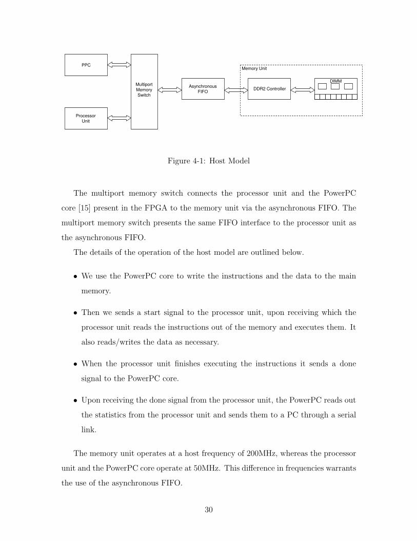
Figure 4-1 shows a schematic of the host model as implemented on the BEE2 board.
This schematic can be viewed as an experimental setup for implementing the emula-
tion platform.
29
PPC
DIMM
DDR2 ControllerMultiport
Memory
Switch
Processor
Unit
Asynchronous
FIFO
Memory Unit
Figure 4-1: Host Model
The multiport memory switch connects the processor unit and the PowerPC
core [15] present in the FPGA to the memory unit via the asynchronous FIFO. The
multiport memory switch presents the same FIFO interface to the processor unit as
the asynchronous FIFO.
The details of the operation of the host model are outlined below.
• We use the PowerPC core to write the instructions and the data to the main
memory.
• Then we sends a start signal to the processor unit, upon receiving which the
processor unit reads the instructions out of the memory and executes them. It
also reads/writes the data as necessary.
• When the processor unit finishes executing the instructions it sends a done
signal to the PowerPC core.
• Upon receiving the done signal from the processor unit, the PowerPC reads out
the statistics from the processor unit and sends them to a PC through a serial
link.
The memory unit operates at a host frequency of 200MHz, whereas the processor
unit and the PowerPC core operate at 50MHz. This difference in frequencies warrants
the use of the asynchronous FIFO.
30

4.3 Operation of the Emulation Platform
In this section we provide a cycle-accurate description of how the emulation platform,
described in chapter 3, operates. We do it through an example implementation.
We emulate a processor unit, operating at 1GHz, connected to a memory unit
through a 32-bit channel, operating at 100MHz. The features of the memory unit are
outlined below.
DRAM Type SDRAM
Bitwidth 32
Speed 100MHz
Precharge 20ns
Row Access 30ns
Column Access 30ns
Data Transfer 10ns
Since the host clock rate of the processor unit is one-twentieth of the clock rate
of the processor unit that we are looking to emulate, the emulation platform scales
down the frequency of the target model by 20.
The 128-bit read/write requests from the processor unit are broken down into four
32-bit requests. Similarly, the 128-bit responses from the memory unit are broken
down into four 32-bit responses. The first 32-bit request is treated as a page miss
in the memory unit and has a longer latency equal to the sum of the four latency
parameters given above. The following three 32-bit requests are treated as page hits
in the memory unit and have a shorter latency equal to the sum of column access
time and the data transfer time.
In order to emulate the model described above, we configure the processor wrap-
per, the memory wrapper and the channel through the parameters given below. All
the latency parameters are specified in terms of the processor cycles.
31

Parameter Value
mem lat 1 90
mem lat 2 40
Bitwidth 32
Latency 10
Buffering 1
Table 4.1: Parameter Values for the Example Implementation
4.3.1 Read Requests and Responses
On receiving a 128-bit read request from the processor unit, the processor wrapper
breaks the request down into four 32-bit requests, and sends request 1 down the
channel in cycle 0. The memory wrapper receives request 1 in cycle 10, turns it into
a 128-bit request and sends it to the memory unit. It also sends a credit to the
processor wrapper so that it can send the next request. In order to keep track of time
the memory wrapper also starts its counter, m count.
Cycle Processor Wrapper Memory Wrapper
0 sends req1 -
10 - receives req1
20 sends req2 -
100 - receives req2, sends resp1
110 sends req3, receives resp1 -
140 - receives req3, sends resp2
150 sends req4, receives resp2 -
180 - receives req4, sends resp3
190 receives resp3 -
220 - sends resp4
230 receives resp4 -
Table 4.2: Read Requests and Responses
When m count=90 it accepts request 2 and sends response 1 to the processor
wrapper. The processor wrapper receives response 1 in cycle 110 and sends a credit
to the memory wrapper so that it can send the next response.
32

When m count=130 the memory wrapper accepts request 3 and sends response
2. When m count=170 it accepts request 4 and sends response 3. And finally when
m count=210 it sends response 4, and resets m count to 0. When the processor
wrapper receives response 4 in cycle 230 it combines the four 32-bit responses and
sends the 128-bit response to the processor unit.
In case either the memory unit is unable to accept more requests or the processor
unit is unable to accept more responses, the credit-based flow control prevents the
wrappers from sending more messages down the channel.
4.3.2 Write Requests and Responses
Cycle Processor Wrapper Memory Wrapper
0 sends req1 -
10 - receives req1
20 sends req2 -
100 - receives req2
110 sends req3 -
140 - receives req3
150 sends req4 -
180 - receives req4
Table 4.3: Write Requests and Responses
On receiving a 128-bit write request from the processor unit, the processor wrapper
breaks the request down into four 32-bit requests, and sends request 1 down the
channel in cycle 0. The memory wrapper receives request 1 in cycle 10 and sends a
credit to the processor wrapper so that it can send the next request. In order to keep
track of time the memory wrapper also starts its counter, m count.
When m count=90 the memory wrapper accepts request 2. When m count=130
it accepts request 3. When m count=170 it accepts request 4. It then combines the
four 32-bit requests and sends the 128-bit request to the memory unit. And finally
when m count=210 it resets m count to 0 and gets ready to accept the next request.
33

In case the memory unit is unable to accept more requests, the credit-based flow
control prevents the processor wrapper from sending more requests down the channel.
34

Chapter 5
Analysis and Evaluation
The emulation platform can model various microprocessor memory systems through
the interaction of the processor wrapper, the memory wrapper and the channel, and
through the specification of the parameters mentioned in chapter 3. The platform
is then analyzed for performance through SMIPS benchmarks, and the resource uti-
lization of all the units and wrappers is determined from the Xilinx Synthesis Tool
(XST). In this chapter we present this analysis in detail.
5.1 Experimental Methodology
Table 5.1 describes the parameters for the five different sets of configuration that are
used to analyze the emulation platform. All the latency parameters are expressed as
the number of processor cycles, where the processor target clock frequency (same as
the processor host clock frequency) is 50MHz.
Configuration mem lat 1 mem lat 2 Bitwidth Latency Buffering
A processor unit and memory unit connected directly
B 16 16 128 1 1
C 90 40 32 10 1
D 70 30 32 5 1
E 50 20 32 3 1
Table 5.1: Modeled Configurations with Parameters
35
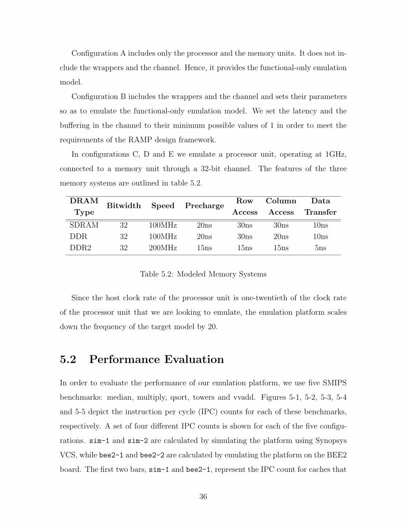
Configuration A includes only the processor and the memory units. It does not in-
clude the wrappers and the channel. Hence, it provides the functional-only emulation
model.
Configuration B includes the wrappers and the channel and sets their parameters
so as to emulate the functional-only emulation model. We set the latency and the
buffering in the channel to their minimum possible values of 1 in order to meet the
requirements of the RAMP design framework.
In configurations C, D and E we emulate a processor unit, operating at 1GHz,
connected to a memory unit through a 32-bit channel. The features of the three
memory systems are outlined in table 5.2.
DRAMBitwidth Speed Precharge
Row Column Data
Type Access Access Transfer
SDRAM 32 100MHz 20ns 30ns 30ns 10ns
DDR 32 100MHz 20ns 30ns 20ns 10ns
DDR2 32 200MHz 15ns 15ns 15ns 5ns
Table 5.2: Modeled Memory Systems
Since the host clock rate of the processor unit is one-twentieth of the clock rate
of the processor unit that we are looking to emulate, the emulation platform scales
down the frequency of the target model by 20.
5.2 Performance Evaluation
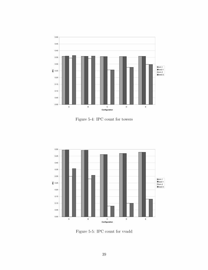
In order to evaluate the performance of our emulation platform, we use five SMIPS
benchmarks: median, multiply, qsort, towers and vvadd. Figures 5-1, 5-2, 5-3, 5-4
and 5-5 depict the instruction per cycle (IPC) counts for each of these benchmarks,
respectively. A set of four different IPC counts is shown for each of the five configu-
rations. sim-1 and sim-2 are calculated by simulating the platform using Synopsys
VCS, while bee2-1 and bee2-2 are calculated by emulating the platform on the BEE2
board. The first two bars, sim-1 and bee2-1, represent the IPC count for caches that
36

have been warmed up, whereas the remaining two bars, sim-2 and bee2-2, represent
the full IPC counts.
The memory units in the simulation platform and the emulation platform are in-
herently different because we are using different memory controllers and the Verilog
DDR2 SDRAM cannot simulate the physical DDR2 SDRAM accurately. These dif-
ferences show up in the IPC counts for configurations A and B, with the IPC counts
for the emulation platform being slightly higher. But these differences disappear
in configurations C, D and E, which proves that the RAMP design framework was
successfully implemented.
The graphs also show that the IPC counts for configuration D are higher than
those for configuration C, and that the IPC counts for configuration E are higher
than those for configuration D. This proves that the bandwidth of the three memory
systems was successfully modeled using the RAMP design framework.
0.00
0.05
0.10
0.15
0.20
0.25
0.30
0.35
0.40
0.45
0.50
A B C D E
Configuration
IPC
sim-1
bee2-1
sim-2
bee2-2
Figure 5-1: IPC count for median
37

0.00
0.05
0.10
0.15
0.20
0.25
0.30
0.35
0.40
0.45
0.50
A B C D E
Configuration
IPC
sim-1
bee2-1
sim-2
bee2-2
Figure 5-2: IPC count for multiply
0.00
0.05
0.10
0.15
0.20
0.25
0.30
0.35
0.40
0.45
0.50
A B C D E
Configuration
IPC
sim-1
bee2-1
sim-2
bee2-2
Figure 5-3: IPC count for qsort
38
0.00
0.05
0.10
0.15
0.20
0.25
0.30
0.35
0.40
0.45
0.50
A B C D E
Configuration
IPC
sim-1
bee2-1
sim-2
bee2-2
Figure 5-4: IPC count for towers
0.00
0.05
0.10
0.15
0.20
0.25
0.30
0.35
0.40
0.45
0.50
A B C D E
Configuration
IPC
sim-1
bee2-1
sim-2
bee2-2
Figure 5-5: IPC count for vvadd
39

Figures 5-6, 5-7, 5-8, 5-9 and 5-10 show the cycles utilized by the memory unit to
process the read/write request. Here again a set of four different cycle counts is shown
for each of the five configurations. sim-1, sim-2, bee2-1 and bee2-2 are calculated
in the same manner as before.
The cycle counts for the simulation platform and the emulation differ slightly for
configurations A and B because of the differences in the memory units of the two
platforms mentioned earlier.
The graphs also show that the cycle counts for configuration D are lower than
those for configuration C, and that the cycle counts for configuration E are lower
than those for configuration D. This proves that the latency of the three memory
systems was successfully modeled using the RAMP design framework.
0
20000
40000
60000
80000
100000
120000
A B C D E
Configuration
Cycle
s
sim-1
bee2-1
sim-2
bee2-2
Figure 5-6: Memory Latency for median
40

0
5000
10000
15000
20000
25000
30000
35000
A B C D E
Configuration
Cycle
s
sim-1
bee2-1
sim-2
bee2-2
Figure 5-7: Memory Latency for multiply
0
10000
20000
30000
40000
50000
60000
A B C D E
Configuration
Cycle
s
sim-1
bee2-1
sim-2
bee2-2
Figure 5-8: Memory Latency for qsort
41

0
5000
10000
15000
20000
25000
30000
35000
40000
45000
A B C D E
Configuration
Cycle
s
sim-1
bee2-1
sim-2
bee2-2
Figure 5-9: Memory Latency for towers
0
10000
20000
30000
40000
50000
60000
70000
80000
90000
100000
A B C D E
Configuration
Cycle
s
sim-1
bee2-1
sim-2
bee2-2
Figure 5-10: Memory Latency for vvadd
42
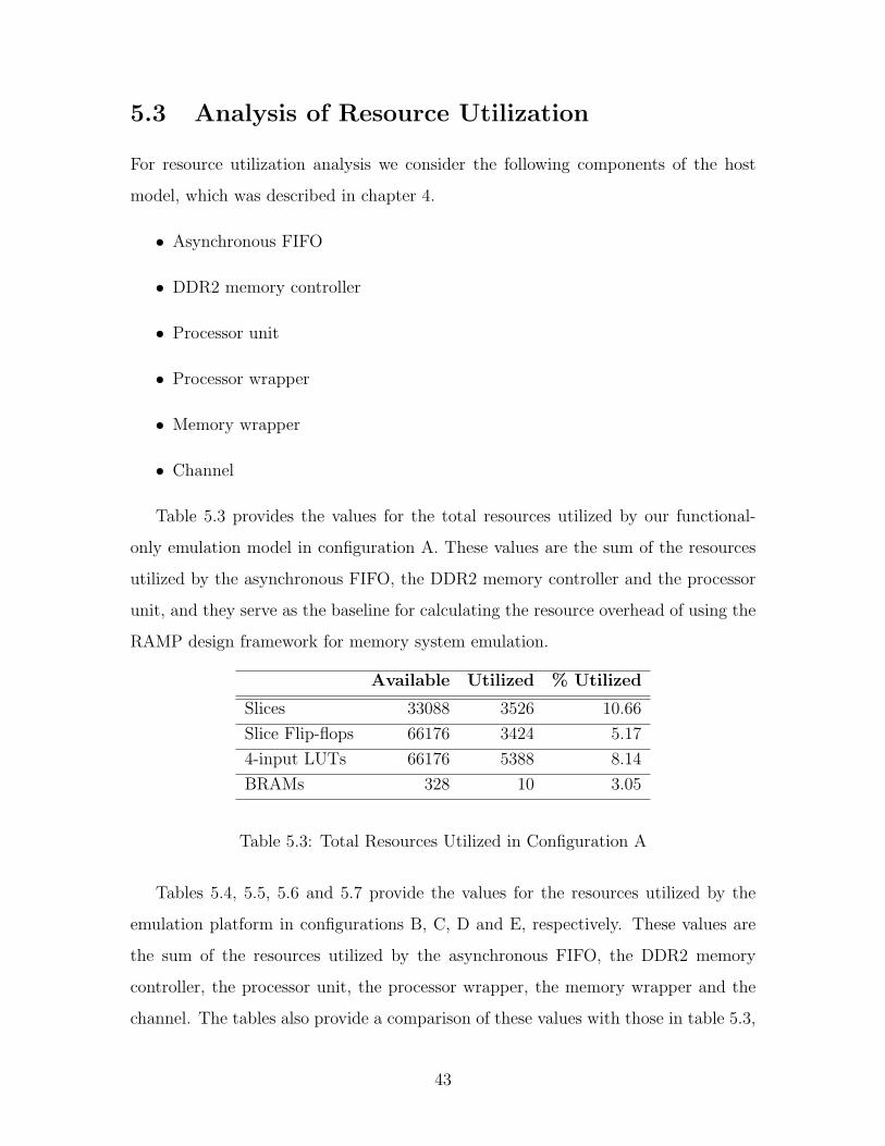
5.3 Analysis of Resource Utilization
For resource utilization analysis we consider the following components of the host
model, which was described in chapter 4.
• Asynchronous FIFO
• DDR2 memory controller
• Processor unit
• Processor wrapper
• Memory wrapper
• Channel
Table 5.3 provides the values for the total resources utilized by our functional-
only emulation model in configuration A. These values are the sum of the resources
utilized by the asynchronous FIFO, the DDR2 memory controller and the processor
unit, and they serve as the baseline for calculating the resource overhead of using the
RAMP design framework for memory system emulation.
Available Utilized % Utilized
Slices 33088 3526 10.66
Slice Flip-flops 66176 3424 5.17
4-input LUTs 66176 5388 8.14
BRAMs 328 10 3.05
Table 5.3: Total Resources Utilized in Configuration A
Tables 5.4, 5.5, 5.6 and 5.7 provide the values for the resources utilized by the
emulation platform in configurations B, C, D and E, respectively. These values are
the sum of the resources utilized by the asynchronous FIFO, the DDR2 memory
controller, the processor unit, the processor wrapper, the memory wrapper and the
channel. The tables also provide a comparison of these values with those in table 5.3,
43

and we see that the resource overhead of using the RAMP design framework is quite
significant in our case.
From table 5.3 it can be noted that the resources utilized by the target model
are quite limited. When we add the wrappers and the channel to the target model,
resource utilization increases quite significantly. The increase will not be as significant
in a multiprocessor emulation platform, the development of which is the goal of the
RAMP project.
Available Utilized % Utilized% Increase from
Configuration A
Slices 33088 4233 12.79 20.05
Slice Flip-flops 66176 4639 7.01 35.48
4-input LUTs 66176 5724 8.65 6.24
BRAMs 328 10 3.05 0
Table 5.4: Total Resources Utilized in Configuration B
Available Utilized % Utilized% Increase from
Configuration A
Slices 33088 4654 14.07 31.99
Slice Flip-flops 66176 5223 7.89 52.54
4-input LUTs 66176 5731 8.66 6.37
BRAMs 328 10 3.05 0
Table 5.5: Total Resources Utilized in Configuration C
Available Utilized % Utilized% Increase from
Configuration A
Slices 33088 4325 13.07 22.66
Slice Flip-flops 66176 4675 7.06 36.54
4-input LUTs 66176 5702 8.62 5.83
BRAMs 328 10 3.05 0
Table 5.6: Total Resources Utilized in Configuration D
44

Available Utilized % Utilized% Increase from
Configuration A
Slices 33088 4229 12.78 19.94
Slice Flip-flops 66176 4481 6.77 30.87
4-input LUTs 66176 5727 8.65 6.29
BRAMs 328 10 3.05 0
Table 5.7: Total Resources Utilized in Configuration E
45

Chapter 6
Conclusion
In this thesis we described the development of an emulation platform for modeling
microprocessor memory systems using the RAMP design framework (RDF). Through
this emulation platform we demonstrated the validity and the efficiency of the design
framework.
RDF aims to provide a standardized design framework to enable high-performance
simulation and emulation of massively parallel systems on a wide variety of implemen-
tation platforms. In this thesis we highlighted the components of RDF and described
how these components interact to provide the emulation platform required for this
research.
The first challenge in this thesis was the development of a target model that would
serve as the basis of the emulation platform. We provided a detailed description of
the various components of this target model and their operation. The next task was
to build a parameterized host model on top of the target model. We discussed the
development of the components of this host model and described their operation and
interaction.
We concluded with an analysis of the performance and an evaluation the resource
utilization of our platform. Using both simulation and emulation in an FPGA, we
showed that the platform successfully modeled both the latency and the bandwidth
of different memory systems.
46

Appendix A
SMIPS Instruction Set
47

48

Bibliography
[1] J. Wawrzynek, D. Patterson, M. Oskin, S. Lu, C. Kozyrakis, J. Hoe, D. Chiou,
and K. Asanovic, “RAMP: Research Accelerator for Multiple Processors,” IEEE
Micro, vol. 27, no. 2, 2007.
[2] G. Gibeling, A. Schultz, J. Wawrzynek, and K. Asanovic, “The RAMP Architec-
ture, Language and Compiler,” University of California, Berkeley, Tech. Rep.,
2006.
[3] K. Oner, L. A. Barroso, S. Iman, J. Jeong, K. Ramamurthy, and M. Dubois, “The
Design of RPM: An FPGA-based Multiprocessor Emulator,” FPGA 95: Proceed-
ings of the 1995 ACM Third International Symposium on Field Programmable
Gate Arrays, pp. 60–66, 1995.
[4] J. D. Davis, S. E. Richardson, C. Charitsis, and K. Olukotun, “A Chip Prototyp-
ing Substrate: The Flexible Architecture for Simulation and Testing (FAST),”
ACM SIGARCH Computer Architecture News, vol. 33, pp. 34–43, 2005.
[5] S. Wee, J. Casper, N. Njoroge, Y. Tesylar, D. Ge, C. Kozyrakis, and K. Olukotun,
“A Practical FPGA-based Framework for Novel CMP Research,” Proceedings of
the 2007 ACM/SIGDA 15th International Symposium on Field Programmable
Gate Arrays, pp. 116–125, 2007.
[6] N. Dave, M. Pellauer, Arvind, and J. Emer, “Implementing a Functional/Timing
Partitioned Microprocessor Simulator with an FPGA,” 2nd Workshop on Ar-
chitecture Research using FPGA Platforms, 12th International Symposium on
High-Performance Computer Architecture (HPCA-12), 2006.
49

[7] D. Chiou, H. Sunjeliwala, D. Sunwoo, J. Xu, and N. Patil, “FPGA-based
Fast, Cycle-Accurate, Full-System Simulators,” 2nd Workshop on Architec-
ture Research using FPGA Platforms, 12th International Symposium on High-
Performance Computer Architecture (HPCA-12), 2006.
[8] D. A. Penry, D. Fay, D. Hodgdon, R. Wells, G. Schelle, D. I. August, and D. A.
Connors, “Exploiting Parallelism and Structure to Accelerate the Simulation
of Chip Multiprocessors,” Proceedings of the 12th International Symposium on
High-Performance Computer Architecture, 2006.
[9] J. Hong, E. Nurvitadhi, and S. Lu, “Design, Implementation, and Verifica-
tion of Active Cache Emulator (ACE),” FPGA 06: Proceedings of the 2006
ACM/SIGDA 14th International Symposium on Field Programmable Gate Ar-
rays, 2006.
[10] F. J. M.-M. et al., “SCOORE: Santa Cruz Out-of-Order RISC Engine, FPGA
Design Issues,” Workshop on Architectural Research Prototyping (WARP), held
in conjunction with ISCA-33, 2006.
[11] L. Augustsson, J. Schwarz, and R. S. Nikhil, “Bluespec Language Definition,”
Sandburst Corp., 2001.
[12] U. C. Berkeley, “DDR2 Controller.” [Online]. Available: http://bee2.eecs.
berkeley.edu/wiki/Bee2Memory.html
[13] Micron, “DDR2 SDRAM Unbuffered DIMM.” [Online]. Avail-
able: http://download.micron.com/pdf/datasheets/modules/ddr2/HTF18C64\
128\ 256\ 512x72A.pdf
[14] C. Chang, J. Wawrzynek, and R. W. Brodersen, “BEE2: A High-End Reconfig-
urable Computing System,” IEEE Design and Test of Computers, vol. 22, no. 2,
2005.
[15] Xilinx, “PowerPC Processor Reference Guide,” 2007. [Online]. Available:
http://www.xilinx.com/support/documentation/user guides/ug011.pdf
50