emips, a dynamically extensible processor for all of the suindicated risc architectures. therefore,...
TRANSCRIPT

eMIPS, A Dynamically Extensible Processor
Richard Neil Pittman, Nathaniel Lee Lynch, Alessandro Forin Microsoft Research
October 2006
Technical Report MSR-TR-2006-143
Microsoft Research Microsoft Corporation
One Microsoft Way Redmond, WA 98052

- 2 -

- 3 -
eMIPS, A Dynamically Extensible Processor
Richard Neil Pittman, Nathaniel Lee Lynch, Alessandro Forin Microsoft Research
Abstract
The eMIPS architecture can realize the performance benefits of application-specific hardware optimizations in a general-purpose, multi-user system environment using a dynamically extensible processor architecture. It allows multiple secure Extensions to load dynamically and to plug into the stages of a pipelined data path, thereby extending the core instruction set of the microprocessor. Extensions can also be used to realize on-chip peripherals and if area permits even multiple cores. The new functionality can be exploited by patching the binaries of the existing applications, without requiring any changes to the compilers. A working FPGA prototype and a flexible simulation system demonstrate speedups of 2x-3x on a set of applications that include games, real-time programs and the SPEC2000 integer benchmarks. eMIPS is the first realized workstation based entirely on a dynamically extensible processor that is safe for general purpose, multi-user applications. By exposing the individual stages of the data path, eMIPS allows optimizations not previously possible. This includes permitting safe and coherent accesses to memory from within an Extension, optimizing multi-branched blocks, and throwing precise and restartable exceptions from within an Extension.
1 Introduction
Most of the many modern available microprocessors implement the Reduced Instruction Set Computer architecture, or RISC, which is based on fixed instruction sets. Many different types of RISC microprocessors populate the market based on these different sets of instructions including, MIPS, ARM and PowerPC to name some of the more popular. These microprocessors are realized in the form of application specific integrated circuits, or ASIC, made up of logic fixed at design time that cannot be altered after the chip fabrication process is complete. When designing instruction sets, computer engineers attempt to capture all the instructions necessary to cover the largest space of potential applications, while keeping in mind factors such as size, cost and power. This set of instructions form the blue print for the
instruction set architecture, or ISA, to be implemented on the new microprocessor. Despite all efforts, the quest for the ‘optimal fixed instruction set architecture’ is an impossible one because the space of applications to which the designers apply general purpose processors evolves constantly. In addition, the trends that govern this evolution shift periodically in response to changes in consumer lifestyles and demands. For example, the need to process more audio and video data has led to extensions for all of the suindicated RISC architectures. Therefore, the selection of instructions for a ‘general purpose’ microprocessor designed to meet the demands of today’s market place may be ill equipped to handle the applications of future markets. We can also argue that the quest for the ‘optimal general purpose’ microprocessor for today’s market does not make sense anymore, especially in the embedded market place. In the embedded market, system designers work within the strictest constraints of size, cost and power. The systems they design apply to a specialized and significantly reduced space of potential applications. In this context, a ‘general purpose’ microprocessor is inefficient and under-utilized when the majority of applications never use a large subset of the capabilities it provides. For instance, many embedded systems rarely if ever use floating point operations but most ‘general purpose’ microprocessors include them. For these applications, a popular solution is to use custom microprocessors with reduced instruction sets but with customized instructions added specifically for the intended application space. This requires redesigning the microprocessor architecture and fabricating custom microprocessors for each of the desired application domains; still they suffer from the inflexibility previously discussed. Therefore, manufacturers cannot offset the cost in design and fabrication of the new custom chip if the market for the given application is not large enough. As demonstrated in this discussion, the problem of this inflexible ‘general purpose’ microprocessor architecture becomes a severe hindrance. What is needed in the embedded application space and potentially in all areas of microprocessor hardware design is a new technology that can provide for flexibility and customization, allowing the microprocessors to evolve with their target markets at all stages of their life cycles.

- 4 -
The Field Programmable Gate Array, or FPGA, is a digital semiconductor device often used for prototyping. Developers use FPGAs in prototyping for the ability to configure or program their electrical interconnects to realize an expansive space of applications from glue logic to application coprocessors. As the name indicates, developers are free to apply modifications to the design implemented on the FPGA in the field, after deployment. Developers synthesize the configurations from a hardware description language, like Verilog or VHDL, for the targeted FPGA device. Eventually, the configuration file downloads to the chip through an interface such as JTAG. This flexibility comes with a price. The configurable logic of the FPGA experiences significantly lower performance, currently clocking at frequencies up to 500 MHz, than the modern ASIC, currently clocking at frequencies over 3 GHz. Despite this limit, FPGA technology has evolved to the point where developers can implement fixed logic microprocessors with performance levels competitive with their ASIC counterparts in the embedded market. These future microprocessors will have the advantage that they can be dynamically updated after deployment to meet new demands. This approach to microprocessor design leads to a new class of microprocessors termed the “dynamically extensible processor”. Using modern FPGAs it is possible to partition the FPGA into sections containing a standard fixed logic processor core with interconnects to blocks termed ‘Extensions’ that contain customized instructions and functionality that loads, modifies and enables while the fixed logic continues to function without interruption. In this way, the dynamically extensible processor, using a library of Extensions from which it can draw, adapts to the changing application needs in the field. By using these dynamically extensible processor cores, a “reconfigurable central processing unit” becomes possible. The eMIPS project described in this document argues that such a device is feasible today and proves this thesis by means of an example prototype implementation.
The standard RISC architecture lacks the infrastructure to allow for the kind of flexibility and extensibility possible through the use of FPGAs. This new extensible instruction set computer architecture provides this infrastructure. The FPGA is partitioned into fixed and reconfigurable regions. The fixed logic region constitutes the base functionality of the processor including security sensitive resources such as the system coprocessor and the systems used by the microprocessor to control its configuration. The Extensions to the base processor make up the reconfigurable region of the FPGA. Alternatively, the fixed logic region can be implemented using ASIC technology and only the reconfigurable region as FPGA or CPLD, with the added benefits of extra security, speed and reduced area. The
eMIPS architecture provides the flexibility and adaptability lacking in the RISC architecture.
The Extensions can take the form of new instructions developed to meet the changing computing needs of the market. The Extensions can be thought of similarly to firmware updates in other devices that load when applications requiring those updated instructions are loaded or of added optional features such as floating point operations. In addition, Extensions can implement optimized instructions that can take the place of blocks of code with the same semantics. In the case of the optimized instructions, these instructions are added to the software binaries immediately before the blocks they replace. If the ‘Extension’ associated with that instruction has been configured to one of the available extension slots in the reconfigurable region of the FPGA, the Extension executes the optimized instruction and the block it replaced is skipped. Otherwise, the data path contained within the fixed region of the FPGA interprets the optimized instruction as a NOP and the original block that is still in the software binary executes normally. The Extension’s custom logic implements the block’s functionality more efficiently than a sequence of instructions that reuses the same execution units to perform the block’s function step by step. For this reason, the Extension executing the same function as the block completes the operation faster. If the block constitutes a large enough percentage of the execution count of the application software the overall performance on this microprocessor is significantly improved. The inclusion of these new instructions requires minimal changes to software binaries, as little as adding the instructions immediately before the blocks they replace.
The eMIPS architecture also addresses the waste associated with including functionality in systems where they are never used. The Extensions of the eMIPS architecture do not load when the microprocessor powers up. The fixed logic system only includes the minimum functionality (system management, reconfiguration support, load, store, arithmetic and logical functions), the Extensions provide any additional functions required by the applications running on the microprocessor. For instance, the floating point co-processor or the media or vector co-processors can be loaded only if and when software applications use them. When applications do not require these functions the Extensions are not loaded, providing for potentially large power savings because the unused Extension slots may have their clocking resources and power disabled to reduce the power consumption. Area savings are also possible because not all Extensions need to be present at all times, as is the case instead for an ASIC implementation. This waste reduction may increase by dynamically loading and unloading not only the co-

- 5 -
processors but also the on-chip peripherals that are part of an embedded microcomputer. Rather than including all possible peripherals in the ASIC we can load them on an extensible processor as Extensions, again with power and area reductions.
The software design techniques for multi-core systems must become more mature before applications can take full advantage of the large-grain parallelism they require. When this happens, the eMIPS technology can be leveraged to realize even greater speedups by providing multiple customized processors executing in parallel. Each processor may additionally execute the instruction blocks that it is best suited for. If the chip area devoted to the Extensions is abundant we can use the eMIPS architecture to realize a more complex and more adaptable multiprocessing system by allowing Extensions to include additional complete data paths, or some other custom processor design. These additional data paths can be loaded on-demand to increase overall throughput. In this way we can convert the eMIPS into a multi-core system when the system is under heavy computational demand. When the system is lightly loaded the Extensions are disabled to save energy and the system reverts to a uni-core system.
Through the use of FPGA configuration technology, the eMIPS architecture addresses the inflexibility, performance growth and waste of the modern RISC architecture. We have realized the architecture in a working prototype, exposing the five stages of the base pipeline to the dynamically loaded Extensions. We have implemented the dynamic loading of Extensions leveraging the Partial Reconfiguration tools and processes provided with the manufacturer’s synthesis tools. The ML401 board we used has enough peripherals that we could create a complete eMIPS workstation and experiment with a multi-user application environment. The flexibility and performance benefits of the architecture have been demonstrated by patching the binaries of a number of software applications and measuring the resulting speedups. We used several software systems, ranging from an object oriented real-time operating system for embedded applications, video games, and the SPEC2000 benchmarks. We find that simple Extensions can easily achieve speedups factors of 2x-3x over the original application binaries, using a very small number of Extended Instructions per application.
The eMIPS system makes the following specific contributions. eMIPS is the first realized workstation based entirely on a dynamically extensible processor that is safe for general purpose, multi-user applications. By exposing the individual stages of the data path, eMIPS allows optimizations not previously possible. This includes permitting safe and coherent accesses to memory
from within an Extension, optimizing multi-branched blocks, and throwing precise and restartable exceptions from within an Extension.
The remainder of this document is structured as follows. Section 2 presents the most relevant background information before introducing the eMIPS architecture in Section 3. The implementation of a first prototype is presented in Section 4, the testing and verification processes are illustrated in Section 5. Section 6 reports the current status of the implementation. Section 7 presents related work.
2 Background
2.1 Shortcomings of Modern ASICS The classical microprocessors have grown
exponentially in speed and complexity while maintaining relative constrained their costs, in a fashion characterized by Moore’s Law. Moore’s Law states that the complexity of modern integrated circuits with respect to cost doubles every two years. One may observe this trend as the various microprocessor manufacturers; including Intel and AMD, vie for supremacy in the market by delivering increasingly faster and more complex microprocessors with new features that augment their capabilities while maintaining fairly level costs over time. As manufacturers reach the limits of the physical constraints of the materials available in terms of speed, conductivity, size and reliability, they also reach the end of this level of growth under current microprocessor design paradigms. With eMIPS the performance gains do not come exclusively from higher clock rates but effectively from devoting more and more area resources to specialized implementations of frequently executed software operations.
The current trend in the quest for additional execution speed provides additional processing cores in the central processing unit and to parallelize the execution of as much of the software as possible. This paradigm has potential, but its effectiveness has been limited by the difficulties involved in parallelizing software that was written for sequential execution, resulting in cumbersome dependencies. These dependencies require extensive changes in the software design paradigms if this approach means to reach its full potential. The eMIPS processor departs from the current techniques for attaining microprocessor execution speedups because it does not require any changes in software design and it is hidden from developers at the software level. To utilize the

- 6 -
Extensions, only minimal changes are required at the assembly/binary level.
2.2 MIPS Instruction Set The MIPS instruction set [ 10 ] provides a good
example of a modern RISC instruction set architecture, although it is but one of many. There are other RISC ISAs available such as the ARM and PowerPC that arguably could be better than the MIPS ISA. Unfortunately, these ISAs fall under proprietary controls that removes them from consideration in research projects such as this. The MIPS documentation for the MIPS R16000 is widely available and by residing in the public domain where most other instruction sets are proprietary, it makes MIPS an ideal choice for research in microprocessor architecture and design. The MIPS instruction set architecture like all fixed RISC architectures has experienced growth, modification and expansion in order to keep up with the changing needs of the microprocessor market. The architecture is currently in its ninth generation with the MIPS R16000. For this reason, the MIPS R4000 was chosen as the basis of the eMIPS processor. In order to consider a device a MIPS microprocessor, all the basic instructions must be implemented. Software compiled using this base instruction set must run on the eMIPS microprocessor and existing compilers for high-level programming languages that target the R4000 should remain usable without change.
The MIPS architecture is pipelined to provide improved throughput at higher clock frequencies. One can increase the clocking frequency by breaking the instruction execution within the processor into stages that require less time to execute. Each stage of the pipeline works on different instructions at different times and then passes the instruction to the next stage to continue execution. After the pipeline is full, the microprocessor completes execution of one instruction per clock cycle just like the non-pipelined version except at a much higher clock rate. This architecture results in a net increase in throughput despite the overhead that the architecture experiences with flow control, hazards and exceptions. The time to fill the pipeline is negligible.[ 9 ]
The classic implementation of the RISC pipeline architecture [ 9 ] includes five pipeline stages: Instruction Fetch (IF), Instruction Decode (ID), Instruction Execute (IE), Memory Access (MA) and Writeback (WB). The functions of these stages are as follows:
• Instruction Fetch (IF) – Update the program counter, or PC, and fetch the instruction located in memory at the address stored in the PC.
• Instruction Decode (ID) – Using wired logic, decode the instruction passed from IF into control signals that control the remainder of the pipeline. Read any data required by the instruction from the general purpose register file. Test branch conditions and calculate the memory location of the next instruction to be executed.
• Instruction Execute (IE) – Using an Arithmetic Logic Unit, or ALU, and other special purpose logic perform operations on data based on the control signals passed from ID.
• Memory Access (MA) – In case of a load or store instruction, the output of IE is used as the memory location to be read from or written to. Otherwise, the output of IE is passed through.
• Writeback (WB) – In the event a register in the general purpose register file is modified by the instruction, the output of MA is written to the desired register.
To realize greater throughput at higher frequency,
some microprocessor implementations have utilized as many as eight pipeline stages. The deeper the pipeline is the greater the overhead in the event of a branch event, hazards and exceptions on execution. To further offset this overhead, microprocessor designers have developed a variety of features, including branch predictors and speculated execution. These features have highly complex implementations and exist beyond the scope of this project. For this reason, the architecture of the eMIPS processor omits these features and has just the basic five pipeline stages.
2.3 FPGA Architecture, Self and Partial Reconfiguration
Some of the new ‘state of the art’ FPGAs, which
have come to market in recent years, have added features that further augment their flexibility and power. First, modern FPGAs, such as the Virtex series from Xilinx Inc. and the Stratix series from Altera Corp., have included a feature called ‘dynamic partial reconfiguration’. FPGAs that include this feature may have their configurations partitioned and later allow individual partitions within the design to continue operations while a new configuration downloads to another partition.[ 14 ] FPGA configuration solutions allow for FPGAs to be configured at runtime by other devices or by themselves. An example of one of these solutions is the System ACE Compact Flash configuration solution. This is an IC chip set that provides five interfaces: JTAG to host PC, JTAG to FPGA, external to a Compact Flash chip, and Control from either the Microprocessor or the FPGA. Using these

- 7 -
interfaces a system can configure one or multiple FPGAs using the JTAG from a PC or reading a configuration from the Compact Flash and streaming it to the FPGAs on the JTAG chain.
Figure 1: Xilinx ML401 Evaluation Board with Virtex
4 LX25[ 20 ]
The FPGA selected for the development and experimentation of this project is the Xilinx Virtex 4 product line1. The Virtex series rates among the most powerful FPGA devices in the market in terms of density, feature set and speeds. These FPGAs clock commonly at frequencies of 100 MHz but the specifications indicate they could operate at much higher frequencies, the specifications claim 500 MHz. These frequencies fall significantly short of modern ASIC frequencies approaching multiple gigahertzes but the FPGAs continue to grow in speed with each new generation. The Virtex 4 high-end FPGAs come in three flavors denoted by LX, SX and FX. Each flavor includes a set of special features to allow developers to select an FPGA with the feature set that best fits their application domain. The Virtex 4 LX targets logic design applications. For this reason, the Virtex 4 LX provides the largest number of logical blocks for implementation. Given the floor planning requirements of partial reconfiguration, having more logic area to work with is preferred. Therefore, the implementation of the eMIPS processor targets the Xilinx ML401 Evaluation board with the Virtex LX25.[ 20 ]
The eMIPS processor uses the dynamic partial reconfiguration feature of the Xilinx FPGAs to implement the dynamic loading of Extensions to the core microprocessor architecture. During the design phase, the core microprocessor architecture resides in the fixed logic 1 The choice of one manufacturer over others was based solely on the author’s familiarity with the tools and devices. For instance, Altera’s devices [ 53 ] should work equally well.
region of the FPGA configuration. The configurable partition(s) constitute the area dedicated to the loading of Extensions after the processor has begun operation. After design implementation completes, the process produces a binary file containing the default configuration. Later the process generates the binary files used to alter the configuration of the extension slots using the default configuration and the hardware description of the Extension as a starting point. At power up, the default configuration contains the implementation of the core microprocessor architecture and the region allocated for the Extensions is empty, or actually contains the minimum logic needed to prevent the synthesis tool from removing it during optimization. When the processor starts an application that requires an Extension, it loads the Extension using a JTAG chain provided by the System ACE configuration solution.
Figure 2: Examples partitioning of a Reconfigurable
FPGA design.[ 14 ][ 5 ]
The System ACE configuration solution provides
functionality needed for the Xilinx FPGA to control and change its configuration. The System ACE configuration solution includes a JTAG configuration chain capable of dynamically configuring the Extensions of the processor. The processor stores the default configuration and the

- 8 -
Extensions in the Compact Flash card interfaced to the System ACE chipset. At power up, the System ACE configuration solution reads the default configuration from the Compact Flash card and streams it on the JTAG chain implementing it on the FPGA. The processor running on the FPGA requests changes to the extension configurations by requesting the loading of a configuration from System ACE through the chip control interface. In this event, System ACE reads the requested extension configuration from the Compact Flash Card. Then like the default configuration at power up, System ACE streams the configuration on the JTAG chain. In the case of a partial reconfiguration, the signals on the JTAG chain only modify the region of the FPGA where the Extension is located. The remainder of the FPGA continues to function normally. Consequently, the processor may continue to execute instructions while the configuration process alters the extension configuration. In this way, the processor power up using the default configuration and modifies its own configuration using the partial extension configurations stored in the Compact Flash Card. 2.3.1 Partial Reconfiguration of Xilinx FPGAs
Xilinx has supported partial reconfiguration since its
Virtex II chip [ 14 ] and that feature continues in the more modern Virtex 4 and Spartan III. Despite the continued support of this feature on their hardware, Xilinx continues to under-emphasize this feature in the tool suite, the ISE Foundation. Xilinx recently released the latest release of the ISE, release 8.2i. In the past, hardware designers performed the partial reconfiguration design flow using command line instructions to the tools in the ISE. Xilinx did not integrate the design flow into the graphical user interface, or GUI of the ISE Project Navigator. This results in a large amount of tedious repetitive steps one must perform to run the design flow. Project management and organization becomes crucial, a large set of files is required for each stage of the design flow. In recent months, Xilinx made a greater effort to provide tool support for the partial reconfiguration and to make it more accessible to developers. A new tool that Xilinx has developed is called Planahead and attempts to provide improved floor planning utilities and to integrate the partial reconfiguration design flow into a project structure managed by a GUI. Planahead currently has limited availability in advanced access beta program.
The smallest reconfigurable unit of the FPGA configuration fabric is called the ‘frame’. When partitioning the FPGA into different independently reconfigurable and static regions the boundaries between these regions must coincide with the boundaries of these
‘frames’. Multiple frames may be grouped together into a single rectangular region. Regions cannot be smaller than a ‘frame’. In the Virtex and Virtex II architectures a frame constituted a column of logic cells called slices that spanned the height of the chip. In the Virtex 4, a column of sixteen slices makes up the ‘frame’. In this way, each column of the Virtex 4 contains multiple frames. In the case of the LX25, which has 192 rows of slices, each column contains twelve frames. This architecture provides the Virtex 4 the advantage of allowing for rectangular regions in the form of tiles on the FPGA configuration fabric as opposed to strictly columns as in the previous architectures.[ 5 ]
Figure 3: Logical connections of signals cross region
boundary.[ 5 ]
Hardware designers must also consider the routing of signals crossing the boundaries of the various regions. Only the region containing the reconfigurable module changes when reconfiguration occurs. The remaining configuration fabric remains unchanged. Therefore any inconsistency from one configuration to the next will result in unpredictable results.
One potential inconsistency can occur when a signal crosses the module boundaries. Consider for instance the case of a signal that crosses the boundary and in one configuration the signal routes through row four but the same signal is routed in row five in another configuration. When the system undergoes reconfiguration, the signal will not line up on the boundary where the reconfiguration occurred, therefore cutting the signal. To prevent this inconsistency we can restrict the routing of such signals to fixed locations along the region boundaries. This is done by passing the signals through a ‘bus macro’ or a hard pre-routed macro positioned on the module boundary and by forcing the router program to route the signal through a given location in each configuration. For the eMIPS processor, bus-macros are placed between the interfaces of the fixed instruction set logic and the dynamic Extensions.
In the Virtex and Virtex II architectures Xilinx provided ‘bus macros’ based on tri-state buffers, or
- 9 -
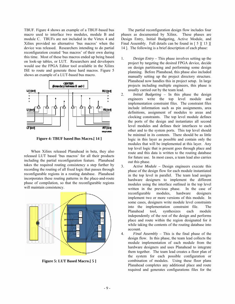
TBUF. Figure 4 shows an example of a TBUF-based bus macro used to interface two modules, module B and module C. TBUFs are not included in the Virtex 4 and Xilinx provided no alternative ‘bus macros’ when the device was released. Researchers intending to do partial reconfiguration created ‘bus macros’ of their own during this time. Most of these bus macros ended up being based on look-up tables, or LUT. Researchers and developers would use the FPGA Editor tool available in the Xilinx ISE to route and generate these hard macros. Figure 5 shows an example of a LUT-based bus macro.
Figure 4: TBUF based Bus Macro.[ 14 ]
When Xilinx released Planahead in beta, they also
released LUT based ‘bus macros’ for all their products including the partial reconfiguration feature. Planahead takes the required routing consistency a step further by recording the routing of all fixed logic that passes through reconfigurable regions in a routing database. Planahead incorporates these routing patterns in the place-and-route phase of compilation, so that the reconfigurable regions will maintain consistency.
Figure 5: LUT Based Macro.[ 5 ]
The partial reconfiguration design flow includes four phases as documented by Xilinx. These phases are Design Entry, Initial Budgeting, Active Module, and Final Assembly. Full details can be found in [ 5 ][ 13 ][ 14 ]. The following is a brief description of each phase: 1. Design Entry – This phase involves setting up the
project by targeting the desired FPGA device, decide on design partitioning and performing some design planning. Before Planahead, this phase also included manually setting up the project directory structure. Planahead now handles this in project setup. In large projects including multiple engineers, this phase is usually carried out by the team lead.
2. Initial Budgeting – In this phase the design engineers write the top level module and implementation constraint files. The constraint files include information such as pin assignments, area definitions, assignment of modules to areas and clocking constraints. The top level module defines the ports of the design and instantiates all second level modules and defines their interfaces to each other and to the system ports. This top level should be minimal in its contents. There should be as little logic in this layer as possible and contain only the modules that will be implemented at this layer. Any top level logic that is present goes through place and route and this data is written to the routing database for future use. In most cases, a team lead also carries out this phase.
3. Active Module – Design engineers execute this phase of the design flow for each module instantiated in the top level in parallel. The team lead assigns hardware designers to implement the different modules using the interface outlined in the top level written in the previous phase. In the case of reconfigurable modules, hardware designers implement two or more versions of this module. In some cases, designers write module level constraints into the implementation constraint file. The Planahead tool, synthesizes each module independently of the rest of the design and performs place and route within the region designated for it while taking the contents of the routing database into account.
4. Final Assembly – This is the final phase of the design flow. In this phase, the team lead collects the module implementation of each module from the hardware designers and uses Planahead to integrate them together. The team lead creates a floor plan of the system for each possible configuration or combination of modules. Using these floor plans Planahead completes any additional place and route required and generates configurations files for the

- 10 -
desired default configuration and other files for the reconfigurable regions that change dynamically.
We used these phases in the eMIPS project. Through
Planahead the eMIPS processor was synthesized, floor planned, components placed, signals routed, and configuration files generated. 2.3.2 System ACE Compact Flash Solution
The System Advanced Configuration Environment,
or System ACE [ 12 ], attempts to fill a niche for pre-engineered configuration solutions of multiple FPGA systems. The system applies to the eMIPS processor’s need to control and modify its extensible configuration architecture. System ACE works through the interaction of four interfaces: JTAG to host PC, JTAG to FPGA, and Compact Flash & Control from Microprocessor or FPGA. Using the host JTAG interface a configuration file can be downloaded manually to the system and used to configure one or multiple FPGAs. This feature is excellent for debugging, it allows the developer to download test configuration and run code before including the new configuration in the system. When configuring the system from the host JTAG the System ACE reads the bits stream on the host interface and transfers it to the system JTAG chain it controls. After the configuration design completes and the system is ready for deployment, system controlled configuration can be performed via microcontroller or FPGA control. In the case of a single FPGA system, like the eMIPS processor, the microcontroller interface can be integrated in the FPGA to allow it to control its own configuration. The Compact Flash is a portable, permanent storage device that stores the configuration files and inserts into a reader integrated with the System ACE. Using the control interface the FPGA or microcontroller can initiate configuration of the system by selecting a configuration file stored in the Compact Flash that the System ACE drives on the system JTAG chain. The System ACE also provides an interface similar to IDE disk interface commonly found on PCs to allow the controller to read and write to the Compact Flash.
The System ACE controller interface provides a 3-bit configuration selection input to allow the controller to select one of eight potential configurations. Note that the Compact Flash can store more than eight configurations, as illustrated in Figure 6. The configurations are grouped into sets of no more than eight and placed in directories on the Compact Flash. In the root directory there exists a file called ‘xilinx.sys’. This file tells System ACE which directory containing configuration files should be considered ‘active’. The controller can only use
configuration files from the ‘active’ directory. The ‘xilinx.sys’ file also assigns to each file the numerical designation zero through seven for the configuration selection. To change which set of configurations is considered active, one must change the assignment in the ‘xilinx.sys’ file. System software can do this dynamically using the IDE interface to the Compact Flash.[ 12 ]
Figure 6: System ACE File structure.[ 12 ]
2.4 Profiling & Identification of Basic Blocks While CPU designers seek generality in their designs,
all application programs spend most of their execution time in small sections of the code that make up the executable file image. This observation holds regardless of platform or application, from personal computers to embedded systems to entertainment consoles and devices. Analysis of software execution profiles revealed that in many cases the two to three most executed sequences of code in the applications program account for more than 80% of the total instruction execution count. Based on this observation, if we can somehow optimize the execution of these few select sequences we can attain an overall improvement of the performance of the entire application.
These sequences are termed the “basic blocks” of the software application. Technically, a basic block is a sequence of instructions that ends in a (conditional) branch and is not branched-to anywhere but at the first instruction. In our work, the basic blocks are identified using the tools distributed with Microsoft Giano [ 22 24 ]. Giano has been used internally at Microsoft Corp. for system verification for some years now. The profiling tool outputs a database of basic block and basic block patterns that manifest in the (set of) application program(s). Roughly speaking, a basic block pattern is the set of all basic blocks that perform the same function but differ in their register assignments or in the embedded constants. Once the database is generated, it is updated

- 11 -
by the simulator each time the profiled application is run. Each basic block is uniquely identified by a hash value, there are no duplicates in the database. Each entry also contains counters for the static and dynamic repetition counts of the block. The static count indicates how many times the block is repeated in the application binary itself, or possibly across more than one binary, according to the user’s preference. The dynamic count is maintained by the execution simulator and counts the times the block has been actually executed during one or possibly more executions of the application. It is possible to obtain the distribution of dynamic counts against time by checkpointing the database with a certain frequency. This can capture the behavior of programs that exhibit “phases” during their execution.
Figure 7: Execution Counts of Individual Basic Blocks
in XQuake, on the Xbox360.
Figure 7 shows the distribution of the top 100 basic blocks in the XQuake video game on the Xbox360 gaming platform. On the Y axis is the dynamic execution count of the individual basic blocks, numerically indexed on the X axis. Other profiling data demonstrate the same two basic traits shown in Figure 7: the graphs drop exponentially and have a rather long tail. In the XQuake case for instance, there are more than 12,500 basic blocks that are executed at least once, against a total population of more than 38,500 individual basic blocks.
To demonstrate the potential speedups that optimizing these basic blocks would deliver, “Extended Instructions” with the same semantics as the basic blocks are added to the simulation of the CPU. Then the profiled application program is ran again, this time with the optimized instructions for the basic blocks inserted into the binary of the software at locations immediately preceding the basic blocks. When the CPU reaches these instructions, it executes the optimized instructions and skips the following block. The idea is that these optimized instructions in the simulation will then become the basis for hardware Extensions of the eMIPS processor. As shown in Figure 8, in the XQuake case this results in a three-fold improvement in the game’s frame rate. Similar
results are obtained with the Doom video game, this time using eMIPS and system software from the Microsoft Invisible Computing, or MIC [ 63 ].
Figure 8: Speedups from Extended Instructions.
Figure 8 then shows the results from the execution of a series of over 40 tests programs that are part of the MIC system. Only one basic block was optimized in these tests, the same in all cases and shown in Figure 9. This optimization is also applicable to the Doom case. The third column shows the speedup for the individual test that benefits the most from this optimization. The fourth column shows the cumulative speedup across all tests.
Column five and six in Figure 8 report the speedups for two benchmarks from the SPEC2000 suite that were run on eMIPS with MIC. Porting of other benchmarks is in progress. Other experiments reported in the literature [ 28 , 29 , 31 , 33 , 37 ] similarly show that replacing basic block sequences with optimized instructions results in a speedup from factors of two to factors of five and in some cases over a factor of ten.
In the practice, the basic block sequences are given to hardware design engineers as specifications, so that they can create a hardware module that implements the semantics of that sequence in the most optimized way possible and in a manner that conforms to the Extension interface of the processor. Automatic generation of the Extension appears feasible [ 31 60 ] but it is beyond the scope of this project and we will assume manual generation. The engineers create the design for the Extension and generate the FPGA configuration file. The configuration file integrates into the application software package. When the application starts up on a platform that supports it the Extension is loaded in a free Extension Slot, provided one is available. If the platform does not support Extensions, or if the security settings of the platform disallow it or if the configuration file is damaged

- 12 -
the Extended Instruction is ignored and the basic block sequence executes normally.
Figure 9: A Basic Block Augmented with an Extended
Instruction
The implementation of the Extension and its use in the application is abstracted and hidden at the software level. No change to the higher level compiler is necessary. After the basic block is identified, implemented and encoded into an Extended Instruction, another tool independent of the compiler augments the executable image. The tool scans the assembly binary image for occurrences of the basic block pattern identified in the profile database; it encodes the new Extended Instruction to match the register assignments and constants, and inserts the new Extended Instruction immediately before the instance of the basic block pattern. In this way, the software is not aware of the hardware acceleration and need not be aware of it.
Figure 9 shows the basic block that was found to be the most frequently executed during the tests of Figure 8. This block was the dynamically most frequent one, it was not the statically most frequent. It was only through actual execution profiling that we found it to be the best candidate for optimization. Simple inspection of the binary code base pointed to a completely different block. The first instruction in Figure 9 is the Extended Instruction, inserted before the block itself. The block is part of a software implementation of a 64-bit division. It shifts left by one the 128-bit number contained in the register quad t0-t1-a0-a1, then makes a conditional branch depending on register t1 being greater than register a2.
The Extended Instructions must conform (at least in part) to the instruction format restrictions of the ISA from which they are derived. In the case of the MIPS ISA, instructions consist of a 32-bit value including an opcode, up to two operand registers and a destination register or data immediate. If this single instruction must replace a possibly long sequence of several instructions with as few
as two operands per instruction, one destination and data, the question becomes how to encapsulate all that information into a 32 bit instruction. One way is to leverage the relationships that exist between operands, destinations and immediate values. For instance, if the register operand of one instruction is the same as the destination of a previous instruction it only needs to be encoded once. Scratch registers need not be encoded, for instance in Figure 9 we can skip the scratch register t3. Notice though that in the implementation of the Extension care should be taken to maintain the same semantics as the original sequence and to write this new value to the register file even if nothing else uses it. When registers differ, the relationships between register numbers can be built into the instruction decoding phase of the Extension. For instance, if there are two registers used by different instructions in a sequence but the second is always one away from the first, the Extension designers only require one of the register numbers to encode both of them. In Figure 9 this is the case both for t0-t1 and for a0-a1-a2. It is up to the binary patching tools to verify that these constants are met. Encoding of destination registers can be performed in the same way. In the case of immediate values, if the value is the same every time the block is executed, then this may be encoded directly into the Extension. This is not the case in the example of Figure 9 and the immediate field must be used, reducing the number of available slots for register numbers by one.
Similar relationships can be identified amongst operand registers to reduce the number of bits (register numbers and the like) needed to encode the required data in the instruction format. If hardware designers cannot reduce the required register numbers to two operands and one destination they could violate the ISA rules and use any of the bits other-than the opcode as they see fit. The only penalty is that a disassembler will not be able to provide any meaningful decoding of the Extended Instruction. Yet another possibility is to further break up the sequence into two or more Extended Instructions. More information, including the means to automatically identify patterns of instruction sequences and applying such patterns to modify executable binaries is presented in [ 36 ].
Using the eMIPS mean of execution acceleration requires no change in software design or practice. Modifications are applied after the software development process is complete, to the finished product. This is in sharp contrast to multi-core parallel systems that require parallelization of the software design at the highest levels to benefit from the hardware feature. Future business models for platform manufacturers that utilize processors include independent services to profile and augment

- 13 -
application software binaries with an Extension to fully utilize hardware acceleration.
3 Dynamically Extensible Processors The eMIPS processor is a ‘dynamically extensible
microprocessor’ because it is based on a new, extensible architecture. The architecture is extensible because it allows additional logic to interface and interact with the basic data path at all stages of the pipeline. The additional logic, which we term Extensions, can be loaded on-chip dynamically during execution by the processor itself. The architecture therefore possesses the unique ability to extend its own ISA at run-time. To explain this more in detail, we will first describe the ‘classical’ CPU RISC architecture in Section 3.1 and then show where the processor architecture departs from it in Section 3.2 and Section 3.3. The overall functioning of a complete system based on an eMIPS microprocessor is then described in Section 3.4.
3.1 The ‘Classic’ RISC CPU Figure 10 presents a block diagram of a ‘classic’
RISC CPU organization, including five pipeline stages, a general purpose register file, a memory interface that includes the interface to the peripherals and a system coprocessor. The five pipeline stages include Instruction Fetch (IF), Instruction Decode (ID), Instruction Execute (IE), Memory Access (MA) and Writeback (WB). The stages are as described in Section 2.2. It is important to note the inclusion in this organization of two Floating Point Units, or FPU, depicted as operating in parallel with the IE block. Execution of floating point arithmetic and other operations require considerably longer execution times to complete than most integer operations performed by the Arithmetic Logic Unit, or ALU, inside of the IE block. These FPUs operate on data in register files that are independent of the general purpose register file used by the rest of the CPU. Independence of the data in these units removes potential conflicts and dependencies and allows these functional units to execute in parallel with the rest of the CPU. Parallel execution limits the latency effects of these floating point operations to those tasks dependent on their outputs. The presence of two FPUs in the diagram denotes the established practice of including multiple instances of functional units on a single chip to achieve a higher rate of instruction throughput. Several other functional units available in modern high-performance microprocessors have been omitted from this diagram for simplicity. These functional units go beyond
the scope of this project and have been omitted from the design.
Figure 10: Block diagram of a typical pipelined CPU
architecture.
Figure 10 depicts the FPUs using different colors to signify that it differs from the other blocks in important ways. In the first place, unlike the other blocks in the diagram the processor does not require these units to function correctly. Floating point operations could be performed in software, using the ALU, although at a significant execution time penalty. Many applications in embedded systems never use floating point operations and it is fairly common to omit these functional units from simpler microprocessors. The omission results in smaller chips, lower power and reduced costs for the embedded market. In the second place, system software has the capability of disabling access to these functional units when switching between software tasks and of restricting use of these units to particular tasks. When restricting access to the FPUs the state of the FPU is preserved across context switches for the benefit of that particular task. This eliminates the swapping of the FPU register file in and out to memory and increases overall system performance.
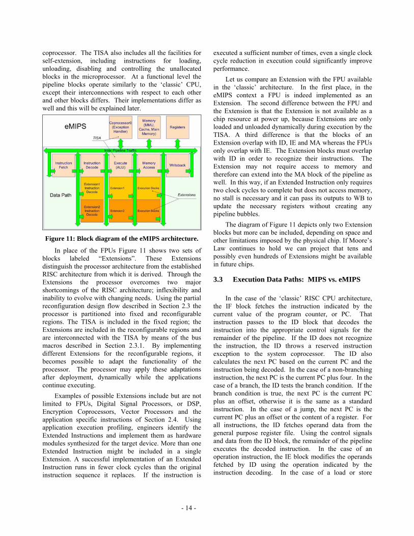
3.2 The eMIPS Architecture Figure 11 presents a block diagram of the eMIPS
processor organization. The pipeline stages, general purpose register file and memory interface match those depicted for the ‘classic’ CPU and are depicted in lighter color in the diagram. These pipeline stages constitute the Trusted ISA or TISA, the core portion of the architecture that is required for initial operation and to provide a level of trust in the functioning of the processor. These blocks cannot be removed or disabled and must be present at startup of the system. These blocks constitute the fixed partition of the architecture and include all resources that are of a security sensitive nature, such as the system
- 14 -
coprocessor. The TISA also includes all the facilities for self-extension, including instructions for loading, unloading, disabling and controlling the unallocated blocks in the microprocessor. At a functional level the pipeline blocks operate similarly to the ‘classic’ CPU, except their interconnections with respect to each other and other blocks differs. Their implementations differ as well and this will be explained later.
Figure 11: Block diagram of the eMIPS architecture.
In place of the FPUs Figure 11 shows two sets of blocks labeled “Extensions”. These Extensions distinguish the processor architecture from the established RISC architecture from which it is derived. Through the Extensions the processor overcomes two major shortcomings of the RISC architecture; inflexibility and inability to evolve with changing needs. Using the partial reconfiguration design flow described in Section 2.3 the processor is partitioned into fixed and reconfigurable regions. The TISA is included in the fixed region; the Extensions are included in the reconfigurable regions and are interconnected with the TISA by means of the bus macros described in Section 2.3.1. By implementing different Extensions for the reconfigurable regions, it becomes possible to adapt the functionality of the processor. The processor may apply these adaptations after deployment, dynamically while the applications continue executing.
Examples of possible Extensions include but are not limited to FPUs, Digital Signal Processors, or DSP, Encryption Coprocessors, Vector Processors and the application specific instructions of Section 2.4. Using application execution profiling, engineers identify the Extended Instructions and implement them as hardware modules synthesized for the target device. More than one Extended Instruction might be included in a single Extension. A successful implementation of an Extended Instruction runs in fewer clock cycles than the original instruction sequence it replaces. If the instruction is
executed a sufficient number of times, even a single clock cycle reduction in execution could significantly improve performance.
Let us compare an Extension with the FPU available in the ‘classic’ architecture. In the first place, in the eMIPS context a FPU is indeed implemented as an Extension. The second difference between the FPU and the Extension is that the Extension is not available as a chip resource at power up, because Extensions are only loaded and unloaded dynamically during execution by the TISA. A third difference is that the blocks of an Extension overlap with ID, IE and MA whereas the FPUs only overlap with IE. The Extension blocks must overlap with ID in order to recognize their instructions. The Extension may not require access to memory and therefore can extend into the MA block of the pipeline as well. In this way, if an Extended Instruction only requires two clock cycles to complete but does not access memory, no stall is necessary and it can pass its outputs to WB to update the necessary registers without creating any pipeline bubbles.
The diagram of Figure 11 depicts only two Extension blocks but more can be included, depending on space and other limitations imposed by the physical chip. If Moore’s Law continues to hold we can project that tens and possibly even hundreds of Extensions might be available in future chips.
3.3 Execution Data Paths: MIPS vs. eMIPS In the case of the ‘classic’ RISC CPU architecture,
the IF block fetches the instruction indicated by the current value of the program counter, or PC. That instruction passes to the ID block that decodes the instruction into the appropriate control signals for the remainder of the pipeline. If the ID does not recognize the instruction, the ID throws a reserved instruction exception to the system coprocessor. The ID also calculates the next PC based on the current PC and the instruction being decoded. In the case of a non-branching instruction, the next PC is the current PC plus four. In the case of a branch, the ID tests the branch condition. If the branch condition is true, the next PC is the current PC plus an offset, otherwise it is the same as a standard instruction. In the case of a jump, the next PC is the current PC plus an offset or the content of a register. For all instructions, the ID fetches operand data from the general purpose register file. Using the control signals and data from the ID block, the remainder of the pipeline executes the decoded instruction. In the case of an operation instruction, the IE block modifies the operands fetched by ID using the operation indicated by the instruction decoding. In the case of a load or store

- 15 -
instruction, the IE calculates the address to be loaded or written to and passes it to the MA block. Using the address calculated by the IE, the MA loads the contents of that address from memory or modifies it using data read from a register in ID. For operation instructions, the MA block passes the result of IE directly to WB. Finally, if the instruction modifies a register in the general purpose register, WB writes the new value of the register to the register file.
The eMIPS follows a similar execution path for instructions included in the TISA. For instructions not in the TISA, the processor departs from this execution path in the ID phase where the ID blocks of the Extensions operate in parallel with the one in the TISA. After the IF block fetches the current instruction from memory, the instruction is sent in parallel to the ID blocks of the TISA and of each Extension. Each ID of the blocks attempts to decode the instruction in parallel. If the TISA recognizes the instruction, the execution path is the same as the previous example of the ‘classic’ CPU. In the case that none of the ID blocks recognize the instruction, the TISA ID block will throw a reserved instruction exception to the system coprocessor like the ‘classic’ CPU model.
If one of the Extensions recognizes the instruction, its ID requests to take over execution of the instruction. The ID arbitration logic sends a NOP to the TISA pipeline stages and to those of the other Extensions. The arbitration logic also passes control of the read ports of the general purpose register file to the ID of the Extension that recognized the instruction. The ID of the Extension that recognized the instruction finishes decoding the instruction and passes the operand data from the register file and control signals to the IE block of the Extension. In general, the instruction decoding may be implemented in logic but for a more flexible design a content addressable memory, or CAM, is preferred. The IE block of the Extension may span the IE and MA block of the TISA, allowing it an additional clock signal of execution time to complete the designated operation. When operations require additional clock cycles an IE of the Extension sends a signal to the hazard detection unit of the TISA to stall the processor until the Extension has completed operations. The IE of the Extension completes execution of its implemented instruction and passes the results to the WB block of the TISA. Other issues exist arbitrating between the TISA and the Extensions and in controlling this more complex data path and they will be identified and addressed in Section 4.
3.4 The eMIPS Workstation Figure 12 illustrates the two ways in which a
workstation based on the eMIPS processor differs from a
regular workstation. In the first place, at power up time the TISA is loaded in the FPGA if it is implemented as the default configuration. If it is implemented in fixed logic this step is not necessary. If the step is necessary, a secure component verifies the validity and integrity of the configuration bitfile and loads it on the FPGA [ 25 ]. In the second place, when a user starts a program that uses an Extension the Operating System asks the TISA to verify and load the Extension Bitfile and enables it for that particular process. Other processes can later share the Extension. For those Extensions that are in fact peripherals the corresponding software entity is a device driver. A multi-core Extension is loaded directly by the operating system, automatically as appropriate.
Figure 12: The eMIPS Workstation, Concept
When the execution reaches a basic block accelerated by an Extension, the Extension will execute its optimized Extended Instruction and skip the block that the instruction replaced. If for any reason the Extension is not available the Extended Instruction is ignored and the software executes normally. To accomplish this evolution of the eMIPS processor within a system some software support is required. Some of this software support was described in Section 2.4, namely the software profiling tools used to identify the basic blocks to be implemented as Extensions. Additional changes to the operating system software are required to control the loading of Extensions and to activate them when they are available.
The operating system is notified of the Extension requirements at application loading time, either explicitly by invoking some API, or implicitly by information contained in the executable file image. The operating system keeps track of the Extension information on a per-process and per-processor basis, as part of its protected state. Figure 13 depicts the additional state that is required for a dual-multiprocessor using the extensible processor of Figure 11. Notice that it is necessary to keep
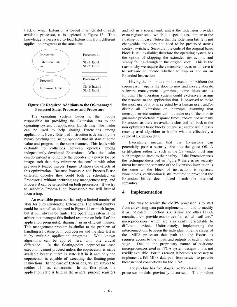
- 16 -
track of which Extension is loaded in which slot of each available processor, as is depicted in Figure 13. This knowledge is necessary to load Extensions from different application programs at the same time.
Figure 13: Required Additions to the OS-managed
Protected State, Processes and Processors
The operating system loader is the module responsible for providing the Extension data to the operating system, at application launch time. The loader can be used to help sharing Extensions among applications. Every Extended Instruction is defined by the binary patching tool using opcodes that all start at some value and progress in the same manner. This leads with certainty to collisions between opcodes among independently developed Extensions. What the loader can do instead is to modify the opcodes in a newly loaded image such that they minimize the conflict with other previously loaded images. Figure 13 shows the effects of this optimization. Because Process-A and Process-B use different opcodes they could both be scheduled on Processor-1 without incurring any management trap, and Process-B can be scheduled on both processors. If we try to schedule Process-1 on Processor-2 we will instead incur a trap.
An extensible processor has only a limited number of slots for currently-loaded Extensions. The actual number could be as small as depicted in Figure 11 or much larger, but it will always be finite. The operating system is the arbiter that manages this limited resource on behalf of the application program(s), sharing it in an efficient manner. This management problem is similar to the problem of handling a floating-point coprocessor and the state left in it by multiple application programs. Well known algorithms can be applied here, with one crucial difference. In the floating-point coprocessor case execution cannot proceed unless the coprocessor is made available because there is state left in it and only the coprocessor is capable of executing the floating-point instructions. In the case of Extensions, we are subject to neither of these constraints. In the first place, the application state is held in the general purpose registers
and not in a special unit, unless the Extension provides extra register state, which is a special case similar to the floating-point case. Notice that the Extension bitfile is not changeable and does not need to be preserved across context switches. Secondly, the code of the original basic block is still available; therefore the operating system has the option of skipping the extended instructions and simply falling-through to the original code. This is the reason why we require the extensible processor to leave it to software to decide whether to trap or not on an Extended Instruction.
Having the option to continue execution “without the coprocessor” opens the door to new and more elaborate software management algorithms, some ideas are as follows. The operating system could exclusively assign the resource to the application that is observed to make the most use of it or is selected by a human user; and/or disable all Extensions on interrupts, assuming that interrupt service routines will not make use of them, or to guarantee predictable response times; and/or load as many Extensions as there are available slots and fall-back to the non optimized basic blocks otherwise; and/or use a least-recently-used algorithm to handle what is effectively a cache of Extension data.
Executable images that use Extensions can potentially pose a security threat to the guest OS. A certification authority, such as the OS vendor must sign such images to attest to their safety. If the Extension uses the technique described in Figure 9 there is no security threat because the semantic of the Extension instruction is the same as the block of instructions it replaces. Nonetheless, certification is still required to prove that the Extension bitfile does indeed match the intended semantics.
4 Implementation One way to realize the eMIPS processor is to start
from an existing data path implementation and to modify it as indicated in Section 3.3. Xilinx and other FPGA manufacturers provide examples of so called “soft-core” microprocessors, which are also easily retargetable to different devices. Unfortunately, implementing the interconnections between the individual pipeline stages of the eMIPS processor data path and the Extensions requires access to the inputs and outputs of each pipeline stage. Due to the proprietary nature of soft-core microprocessors used in FPGA system designs this is not readily available. For this reason, it becomes necessary to implement a full MIPS data path from scratch to provide these needed connections for the TISA.
The pipeline has five stages like the classic CPU and processor models previously discussed. The pipeline

- 17 -
stages include instruction fetch (IF), instruction decode (ID), instruction execution (IE), memory access (MA) and Writeback (WB). The descriptions of these pipeline stages have been outlined in previous sections. The output of the IF block routes to the ID stage of the TISA, the ID stages of each Extension slot and to a CAM. The input to the CAM is the opcode field of the instruction, the output is a set of enable lines, one per Extension slot. Each ID attempts to decode the instruction in parallel using combinatorial logic. The output of the IDs and of the CAM route to an arbitration module that determines which ID has recognized the instruction and who should control execution from that point on. The CAM output is used to arbitrate conflicts between the IDs. Additional logic from the system coprocessor can disable individual IDs.
The general purpose register file connects to the IDs through the arbitration module to allow the winning ID to gather operand data for executing the instruction. The number of read ports on the general purpose register file increases to eight to cope with cases where the Extended Instruction requires more than two operands. The top two read port outputs route to the TISA IE block and all eight route to each of the Extension blocks. The remaining pipeline stages in the TISA remain as they would be for the classic CPU, except the connections between the EX and MA and MA WB pipeline stages are multiplexed with connections to the Extensions. This allows execution in the Extensions to re-enter the normal pipeline at any point.
The data forward and hazard modules of the pipeline are scaled to incorporate connections to the extension slots. The write ports of the general purpose register file and the logic within the WB stage are expanded to accommodate four write ports instead of the standard one. This supports Extensions that produce more than one result and keeps the ratio between read and write ports constant.
The functionality of the system coprocessor increases to let software manage the processor’s extension slots. Additional register numbers, not previously allocated, in the system coprocessor or CP0 are defined to control the state of the Extensions. Bits in these register may enable or disable a given extension slot, and define the behavior when an Extended Instruction is recognized by an Extension that is currently disabled. Two alternatives are to treat the instruction as a NOP or to generate an illegal instruction exception. Some registers are defined to control access to the opcode CAM, in ways similar to the MMU interface. Yet other registers are used to set the priority of the extension slots. If more than one Extension recognizes the same instruction, the Extension with the higher priority wins the arbitration. In this way, if the
Extension has higher priority than the TISA, the Extension may mask an instruction in the TISA. For instance, consider the case of multiplication. If an application requires a lot of multiplications to the point that developers want a more optimized multiplier than what is available in the TISA, an Extension could be developed that includes a faster multiplier but perhaps uses a larger area.
The Extensions have ports that interface to the IF, MA and WB stages of the TISA pipeline. These interfaces conform to a standard that must be applied to all Extensions in order for them to be applicable to the processor’s hardware. These interfaces include control signals from the arbitration unit derived from the outputs of the ID blocks and the status enable/disable bits of the Extension Control Registers in the system coprocessor. The Extensions use the interfaces to the other pipeline stages to pass data to those stages in order to reenter the TISA pipeline and continue normal execution. Extensions requiring more than two clock cycles to complete may stall the pipeline through the hazard detection unit. The status registers in the system coprocessor controls the clocks to the Extensions to reduce power consumption from a disabled Extension.
To realize a complete microcontroller capable of executing test applications the system requires some peripherals integrated on chip in addition to the data path. The minimum set of required peripherals includes the universal serial synchronous asynchronous receiver transmitter, or USART, the interrupt controller, timers, the SRAM interface, the FLASH interface, the parallel input/output interface, or PIO, and the Block RAM interface. The data path accesses these peripherals through the memory interface. The microprocessor’s peripherals map to the memory locations in accordance to a memory map stored in the Block RAM. The Block RAM is a pre-initialized memory element internal to the FPGA that may be used to store data or implement other functions. In this case, the Block RAM is interfaced to the microprocessor as a small internal memory that stores the memory map and the boot loader for the system.
The eMIPS processor at power up or reset starts execution in the boot loader in the Block RAM. The boot loader initializes the peripherals that are available and determines where to jump to begin operation. In our prototype system, after initializing the peripherals the boot loader checks the PIO for the status of a button. If the button is asserted, the boot loader attempts to download the application from the serial line and to write it to the SRAM. After download completes the boot loader jumps to the base address of the application it received to begin execution. If the button is not asserted,

- 18 -
the boot loader jumps to the FLASH and begins executing there.
The rest of this section delves into more details for specific aspects of the implementation that posed us non-trivial challenges.
4.1 Scaling Many area and complexity issues rise out of the need
to scale up some of the components of the data path for the Extensions to work efficiently. Since some Extensions require more than the standard two operand registers allowed in the standard RISC architecture the register file must be scaled up to allow for additional read ports so the Extension may gather all its operand data in parallel and prevent the delay resulting from multiple register accesses to gather all the data. A similar problem exists for the write ports. Most Extensions will modify more than one register in Writeback so additional write ports are needed. In the first prototype the register file has been scaled by four (eight read ports and four write ports) and has significantly grown in size. This disproportionate increase in size versus port numbers is a direct consequence of the modular architecture of the FPGA. The FPGA slices can be easily combined and cascaded to build larger components, but there is an overhead generated by the interconnected blocks. Consider building a 5:1 mux using only 4:1 muxes as the building blocks. It is necessary to route two inputs into one mux and ground the others. The output of the mux is input to a second mux, along with the remaining inputs. In this way it takes two 4:1 muxes to realize a 5:1 mux, three for an 8:1 mux and four for a 12:1 mux. Additional logic is needed to control the switching of these muxes. It is plain to see how this poor scaling results in such growth.
In addition to the register file read and write ports, the hazard detection and data-forwarding units must also be scaled to meet the increased data throughput and they create similar scaling issues.
4.2 Area Challenges The limited physical resources available on the
Virtex 4 LX25 FPGA impose considerable constraints on the design and implementation of the eMIPS processor. In the first place, the FPGA contains only 10752 slices for realizing the logic of the design. [ 18 ] As the processor grows in complexity additional logic is required to realize it. The minimum components to realize the eMIPS processor include the baseline data path (including five pipeline stages, registers, exception handler and pipeline registers), memory interface (including memory mapped
peripherals) and room for the Extensions. To realize a functional device, peripherals such as the SRAM memory interface, USART, Timers, and interrupt controller are required. An interface to the System ACE chipset for reconfiguration is also required. These components in some cases are fairly complex requiring a large number of slices. The reconfigurable feature of the design further constrains use of the physical resources area-wise by requiring the use of bus macros, or pre-routed macros. Bus macros maintain the connections between fixed and reconfigurable logic by forcing all signals that cross the boundary to route a certain way in every configuration. These bus macros are fixed and cannot be optimized away, and their placement is important. For this reason, the bus macros have the potential to create considerable overhead in the design.
Figure 14: Input Coupling Bus Module.
To minimize the impact of the bus macros on the design and to reduce area overall, we strive in the implementation of each module to optimize each component as it is designed. Sometimes this requires revisiting a component to squeeze out a few more slices. To deal the with bus macros themselves, a method of feed-forward input-coupling/output-decoupling is used. Each component has input and outputs that must be routed to multiple other components. In an effort to minimize the number of signals that cross from one component to the next, the inputs of each component are coupled together into a bus-like module that collects all inputs to a component together and then passes them to the component. Inside this bus-like module, signals can be consolidated and optimized to reduce the number of signals that must be passed to the component. In the case of a component that is reconfigurable this reduces the number of signals that must pass through a bus macro and thus reduces the number of bus macros required.
4.3 Pipeline Issues For the eMIPS it is necessary to address issues that
occur in all RISC architectures but that here take on additional requirements. These include pipeline control, exceptions, branches and hazards. The pipeline control is assigned to the ID of the Extension that takes control of the pipeline and these controls propagate through the

- 19 -
pipeline by the pipeline registers as in the standard RISC architecture. The eMIPS diverges from this by adding muxes ahead of the EX, MA, and WB stages. These are needed for path exit and reentry when an Extension is used.
eMIPS uses an exception handling coprocessor to control the state of the microprocessor and to store information about exceptions for later software processing. The coprocessor is augmented with additional registers for controlling the Extension blocks. From the exception handler the Extension may be enabled, disabled and assigned priority. To minimize the number of instructions in the pipeline that are fetched before a branch is tested, RISC processors perform all branch tests and jumps from the ID phase. This explains the strange behavior of branch instructions forcing the execution of the instruction that immediately follow the branch (delay slot) whether the branch is taken or not. A problem arises when data from EX is needed for ID. The data is not guaranteed to be ready in time for it be used in ID so the pipeline must be stalled until the end of EX and forwarded in MA. When the hazard detection unit detects this, it signals a stall to the pipeline. There are two ways to handle data hazards, forward the data and stall. The eMIPS processor utilizes both. If data for a register being written to is in MA or WB, the data is forwarded to ID or EX as appropriate.
The eMIPS pipeline is more complex than the standard RISC pipeline that most readers are familiar with. In addition to the standard issues of the RISC architecture the eMIPS adds the issue of arbitration between the baseline data path and the Extensions. A pipeline arbiter is used as the gateway to the pipeline. When an instruction is decoded the arbiter decides whether the baseline data path or the Extensions will take control. The arbiter receives acknowledgements from the instruction decoders of the baseline data path and the Extensions whether or not an instruction has been recognized. If only one instruction decoder recognizes the instruction the path that is associated with that decoder will normally take control, but there are some special cases that must be addresses. If the instruction is only recognized by a disabled exception, the arbiter must not allow that Extension to take control and prevent the baseline data path from throwing a reserved instruction (RI) exception. When this occurs the microprocessor must interpret the instruction as a NOP. In this case the arbiter uses control registers in the exception handler to verify which Extensions are enabled and which are not. It is also necessary to prevent generation of a false RI exception by baseline data path, and the arbiter is therefore the one responsible for throwing the exception when none of the Extensions recognizes the instruction.
A similar solution is implemented in the case of multiple instruction decoders recognizing the same instruction. In this case the Extension Control Registers assign a priority to each Extension and to the baseline data path. By default, a daisy chain priority is assigned starting from the baseline data path. When conflicts do occur, the Extension or the baseline data path with the highest priority wins control of the pipeline. Finally, if none of the instruction decoders recognize the instruction, the pipeline arbiter should throw a RI exception, except when the application running on the microprocessor uses an Extension and for whatever reason that Extension is not available in the chip. There are two potential solutions for this in hardware and software. In software, the exception handling routing could check a table of Extension op codes and if the op code matches one that is in use, ignore the exception. Otherwise, handle normally. In hardware a similar look up table could be implemented and checked by the pipeline arbiter before throwing the exception.
Figure 15: Pipeline Arbitration Hardware.
In addition to these arbitration issues, the pipeline must include a way for the data control signals traveling down the Extension path to return to the baseline path at some point to complete execution of the instruction by either performing a memory operation or writing back to the register file. The Extension ID determines where the Extension path reenters the baseline path based on the instruction encoding. To reenter the baseline path at either MA or WB the Extension uses a large multiplexer that outputs to the proper pipeline stage where it will reenter the pipeline. These are two to one multiplexers, with the Extension and the previous pipeline stage as inputs. In the case of the a simple Extension, one that requires less than two clock cycles with no memory access, no change in the pipeline clocking pattern is

- 20 -
required. The instruction can execute in step with the pipeline and reenter at the appropriate point. However, in the case of an Extension requiring three or more clock cycles to complete the pipeline will have to stall until the execution is complete and the result is written back. Stalling the pipeline is necessary due to potential dependencies. Any performance penalties this creates could be alleviated by further complicating the pipeline controls. The hazard detection could check for dependencies and only stall if one exists. The pipeline could continue in parallel while the Extension is executing and then the Extension would only have to stall the pipeline long enough to insert the results to be written back to the register file if the a dependency has not already caused the pipeline to stall. This method however, involves considerably more complexity and in this case the commit of instructions would no longer be in order.
Figure 16: Data path Reentry Hardware.
4.4 Exception Processing Replacing an arbitrary sequence of instructions with a
single Extended Instruction can create exceptions (such as TLB misses) at a number of points during execution of the extended instruction. Consider the case of a load instruction that is the third instruction in the original sequence. Should the effective address of the load fail to translate an exception must be reported, according to the MIPS ISA, for a PC at the fourth address in the sequence. The address that failed translation must also be made available to software. If any register was modified by the first or second instructions they must be written back to the register file.
In some cases it is possible to implement this type of Extensions in a transactional style. All resources and address translations are gathered before the instruction
starts and any failure is reported at the starting address. No write-backs are needed and this simplifies exception reporting. Once the instruction starts it is guaranteed to complete and to reach the Writeback stages without incidents.
Figure 17: Instruction Decoding with a CAM.
In more complicated cases this scheme is not
feasible, for instance if an effective address is the result of a preceding load instruction in the same sequence. In these cases the Exception can maintain a virtual PC register that follows the progress of execution, mimicking the progress of the PC in the original sequence. The instruction will proceed to the Writeback regardless, using the partial results. When an exception is reported execution will restart from within the original basic block. This is the main reason why the preferred mean of patching binaries for eMIPS is to insert the Extended Instruction, without damaging the original basic block.
4.5 CAM-based Decoding A more flexible implementation of the instruction
decoding would include a CAM to hold the allowed op codes and control signals stored within. The CAM would be loaded with all the instructions supported by the base line data path. Support for Extended Instructions is implemented by loading the Extension into the FPGA and then writing a new entry into the CAM. The output of the CAM when presented with an instruction will indicate to the pipeline arbiter if the instruction is recognized and if so, whether the baseline data path or one of the Extensions will carry out execution. The same data and control signals are inputted to each of the execution blocks and only the one that is enabled by the pipeline

- 21 -
arbiter executes. The baseline data path is given a NOP when it loses the arbitration like before.
Use of a CAM solves the problem of the limited number of opcodes available to the Extensions and the resulting conflicts as illustrated in Section 3.4.
5 Testing and Verification Tools are needed to ensure that the design and the
prototype of the processor are correct, using both testing and verification. The complexity of the system makes unit testing of individual components insufficient, especially since the interactions between components is of particular interest. The data path derives from a collection of components such as an ALU, shift registers, multiplexers, decoders, etc. Most of these individual components are fairly simple in their implementations. Therefore, interconnects and timing between these components becomes the focus for debugging any improper behavior of the system.
We integrated multiple tools in order to leverage their strengths and to better assist in the verification and the functional testing of the processor. These tools include Mentor Graphics’ ModelSim 6 Xilinx Edition [ 21] and Microsoft Giano [ 22], the same tool previously used for software profiling.
Figure 18: Atmel EB63 Evaluation Board[ 2 ]
Giano simulates a full microprocessor system, initially the Atmel EB63 Evaluation Board depicted in Figure 18. The simulation of this board provided the initial operating environment for the processor. Both Microsoft Research and the Microprocessor Design course at Texas A&M University (CPSC 462) have used this platform for research and educational purposes for
some time, since before 2004. Software for this board was already publicly available and easy to modify, [ 63 ] this well-known platform therefore is a good baseline for comparisons. Later on in the project the processor module and the software have been extended and simulated in a configuration that more closely resembles the target ML401 board from Xilinx. This configuration is shown in Figure 20.
Figure 19: Testing eMIPS with Giano.
In the test environment depicted in Figure 19, two instances of the Giano simulation run in parallel. Both instances run a slightly modified model of the EB63 board. One instance (shown at right) runs with a verified functional model of a MIPS data path in place of the ARM core used in the real evaluation board. This instance records its execution history and sends it to the eMIPS ModelSim simulation. It acts as an ‘Oracle’, providing the correct execution stream of the software application for comparison with the system being tested. The second instance (left) replaces the ARM core with an interface to the ModelSim hardware simulator (center). Inside of ModelSim, a Verilog implementation of the eMIPS data path being tested is running within a wrapper module providing a simulated clock. The data path simulation interacts with Giano through the Verilog Programming Language Interface [ 11 ], or PLI, using memory requests. The data path fetches instructions from the memory simulated in Giano and interacts with the peripherals according to the EB63 memory map. These peripherals are simulated by Giano to better isolate errors in the data path itself. Each time the data path running in ModelSim commits an instruction it checks its internal state against the state reported by the ‘Oracle’ instance of Giano. This allows the Verilog implementation of the data path to verify if it is behaving correctly. When a discrepancy is found the simulation can stop immediately, and the history trace most likely contains all necessary data to find the cause of the error. In this configuration we can execute arbitrary long sequences of instructions, including the bootstrapping of an entire operating system and the loading of application programs.

- 22 -
Figure 20: Peripherals for the ML401 Board.
In addition to the EB63 Oracle environment, another environment was assembled for more exhaustive testing. This environment is called the TestGenerator environment and is shown in Figure 21. This simulation includes the same ModelSim interface (labeled “FPGA” in the picture) and the simulated MIPS processor (“MipsOracle”) used in the previous setup except they are now present in the same Giano instance, connected to the same test pattern generator (“TestGenerator”) that acts as a memory bus interface to both simulated cores. The test pattern generator feeds the simulated cores with the same sequence of instructions and data, and captures the addresses and values of any data written to memory. As the Verilog implementation running in ModelSim commits instructions it compares its state to that of the ‘Oracle’ like in the previous example. The TestGenerator scans the entire core instruction set of the processor (the TISA) and for each instruction generates a sufficient number of tests to guarantee coverage both with respect to the instruction encoding and with respect to the functional results given a set of test values in registers.
Figure 21: The TestGenerator Environment
The data path can be verified using these two simulation environments. Application testing performed by the EB63 and ML401 environments provides confidence that the processor executes the application software like the real eMIPS processor. The exhaustive functional tests performed by the Test Generator ensure that all corner cases operate within specification.
As the data path is tested and verified for correctness, implementation of the on-chip peripherals begins. These peripherals have the potential of becoming complex systems on their own. Unit testing must be performed on some of these peripherals using ModelSim. After the peripherals have been verified in simulation, debugging continues on the FPGAs using test benches based on the simulation. Xilinx Chipscope Pro, an on-chip debugging and verification tool, allows us to monitor the internal signals of the FPGA for this purpose. Using Chipscope, integration testing follows unit testing as these peripherals become interconnected with the data path through the memory map. Eventually, a full system is assembled on the ML401 board using the same software binaries used in the ML401 simulation with Giano.
6 Progress to Date At the time of this writing, development work on the
project is on-going. To date, the data path blocks that constitute the TISA of this first implementation of the eMIPS processor are complete and in the process of being tested. The system can already execute simple test programs. Support for exceptions and interrupts throughout the system is under test by attempting to boot the operating system. Extensions are synthesized but untested. Development of the on chip peripherals continues and testing is being performed as they complete. The implemented peripherals undergoing testing include the universal serial synchronous asynchronous receiver transmitter, or USART, interrupt controller, timers, SRAM interface, and Block RAM interface. Additional peripherals in development include a FLASH interface, Peripheral Input/Output, or PIO, System ACE interface, Watchdog timers, IDE interface and pulse width modulation generators. Each peripheral integrates into the processor’s memory map as it is completed and it is simulated and unit tested before performing integration testing on the FPGA.
Figure 22: eMIPS on the Virtex4-LX25 FPGA Device.
When synthesized for the Xilinx Virtex4 LX25 FPGA a complete eMIPS microcontroller uses the area resources indicated in Figure 22. The data path uses 31-36% of the available area resources, the on-chip peripherals use 21-23%, and the sample Extension of Figure 9 uses 7-9%. The target clock frequency is 100 MHz.

- 23 -
7 Related Work The concept of using reconfigurable logic to improve
application performance is certainly not new [ 47 ] but to date not enough progress has been made towards an actual implementation of this and related concepts in a complete, usable and safe multi-user system.
One difficult point is addressing the security risk posed by the potentially tamperable FPGA execution engine [ 42 ]. Bossuet et al. [ 25 ] looked at FPGA security in the sense of securing the reconfiguration bitfile and protecting the IP contained therein. This is a good contribution, but only solves one aspect of the problem. There are a number of FPGA-based “accelerator” products [ 56 57 55 ] that restrict the use of the accelerator to a single process. This conservative approach still fails to secure other users from a virus injected into the one process that uses the accelerator. Dales [ 35 ] simulates a system that can leverage the FPGA acceleration in a general purpose workstation environment, switching the device among many applications. The FPGA is interfaced as a co-processor, security issues are not really addressed. Many other projects have simulated similar systems [ 40 39 43 44 45 ], ours is the first attempt to actually build a FPGA-based extensible microprocessor and a workstation that is safe for general, multi-user application loads.
One way to classify the various designs is in the way they interface the configurable logic to the main processor. Some use a memory mapped interface or FIFO, most likely over an I/O bus [ 56 57 55 17 ], some use separate co-processors and explicit communication [ 17 41 39 40 44 46 61 ] others implicitly communicate using hints in regular (branch) instructions [ 7 ]. In eMIPS the programmable logic plugs directly into the pipeline and is accessed by explicit, per-application instructions.
Razdan and Smith [ 39 ] designed and simulated the PRISC system, the first system to use the idea of augmenting the pipeline of a MIPS processor with special instructions that are actually executed (on a per-process basis) in a reconfigurable logic array, the Programmable Function Unit, or PFU. They did not consider letting the PFU stall the pipeline, or access memory. They envisioned using the compiler to leverage the new, generic instructions but actually just patched binary objects in their experiments. The required system support was not addressed and PRISC was never physically realized. Garp [ 40 ] was also not realized; it improved on the PRISC design by considering system support, albeit in the expensive form of swapping the content of the entire logic array in and out to main memory at context switch time. The logic array was controlled using a clock counter
to enable/disable its clock and to synchronize with the main processor’s instruction stream. This results in a heterogeneous multiprocessor of sorts that requires both sophisticated compiler support and parallel programming expertise. The security threat of a direct path to memory was not considered but it does permit (physically addressed!) load/store operations that most other designs cannot handle. Borgatti et al. [ 99 ] have recently realized a system similar to Garp, using a mixture of ASIC and embedded FPGAs. This system is reminiscent of the eMIPS if we map the ASIC component to the TISA and the FPGA to the extension slots. Unlike eMIPS though, the interface between FPGA and datapath is limited to stopping the clock to the ASIC module when the slower FPGA needs more time. There is no access to the register file, memory accesses are only to a local buffer, and there is no MMU and no consideration to multi-user safety. Borgatti’s work does study the practical problems that arise from integrating the slower and larger FPGAs into a 90 nm ASIC process, but the actual prototype chip only runs at about 100 MHz like our ML401 board.
Lysecky et al. [ 45 ] imagine a processor that is capable of auto-optimizing itself. Much like eMIPS, the Warp processor would optimize the frequently executed blocks of code by keeping frequency counts to detect the most frequently executed ones, automatically generate custom logic for their direct execution through micro-CAD on-chip tools, and patch the binaries of the executing programs to execute faster. While certainly ambitious and rather impractical, this approach still does not address issues that are important in a practical system, such as security, multiprogramming and virtual memory support.
Clark et al. [ 7 ] propose using a reconfigurable dataflow engine as a co-processor that semi-transparently augments a regular RISC processor. This approach uses a hardware accelerator that identifies execution patterns based on execution tree compression and some compiler help. Using this pattern recognition, the accelerator controller configures the reconfigurable dataflow engine to realize the pattern in a fixed number of cycles rather than in the data path. This approach falls short of this work in three respects. In the first place, it requires considerable modification of the software compiler to recognize the candidate code fragments and generate basic blocks that are recognizable by the runtime engine. The eMIPS does not require any change in the software tools and processes. In the second place, the dataflow engine has limited depth and applicability and this limits the performance benefits achievable with this approach. With eMIPS the pipelined can be stalled and all blocks are accessible, including memory accesses. In the third place, the approach was only tested using a modified

- 24 -
SimpleScalar simulator [ 23 ] and did not result in a practically usable prototype. We intend for our prototype to be freely available to the research community for full evaluation and modification, thereby allowing the practical testing of this and other approaches.
Athanas and Silverman [ 3 ] did produce a prototype, the PRISM I. This approach also focuses attention on the compiler, specifically a C compiler that produces both software and hardware binaries targeted to the platform. According to [ 3 ] there are several limitations in the implementation that do not apply to this work. These include the inability of the PRISM I to support global variables in its hardware extensions, exit conditions for for-loops must be determined in advance, not all of the C functions have been implemented and floating point operations are not supported. These limitations are now largely addressed by more recent systems that use a similar architecture and a similar software approach. For instance, Altera Corp. C2H compiler [ 41 ] targets an FPGA with a hard-core CPU and lets the user easily partition a C application in functions running on one or the other engine. The eMIPS processor provides transparency to users at the software level and uses a deeper coupling between custom logic and the data path. Any MIPS compiler can be used for the eMIPS, for any programming language. Similar considerations apply to the many other C-to-gates flows [ 62 ] and, at least in part, to Anderson’s HThreads hybrid system [ 52 ].
Sawitzki et al. [ 48 ] realized CoMPARE, a simple and cheap 8-bit extensible processor similar to Davidson’s RM [ 59 ]. The limitations of these practical systems illustrate very well the gap between simulation and reality in this field of research.
Chow et al. [ 43 44 58 ] introduce OneChip, motivating the need for a close coupling of the data path and reconfigurable logic. While the basic idea is similar to those explored in eMIPS, the three different implementations of OneChip differ each in its own way. OneChip-96 [ 43 ] is a small subset that does not provide reconfiguration other than at boot time, processor and extensions are literally compiled together. Interestingly, one of the two examples provided is for a peripheral, a USART. OneChip-98 [ 58 ] uses a dedicated path to memory like Garp and suffers from the same memory coherency and security problems. The instruction encoding is now fixed and based on the notion of copying data in and out of the FPGA array, similar to the PRISM I based systems. One extended opcode is reserved for FPGA use, four additional bits select the specific Extension. The actual implementation is very constrained and does not provide dynamic reconfiguration or memory coherence. There is no system software, or interrupts of any type. Two test programs demonstrate 10x-32x
speedups. OneChip-01 [ 44 ] does away with an actual implementation and is simulated using SimpleScalar.
The Xtensa architecture [ 51 , 54 ] has similarities with eMIPS and two important differences. In the first place, Xtensa processors are realized as ASICs, based on the customer’s application requirements. They are statically extensible processors and are therefore subject to the limitations previously illustrated for a classic RISC processor. In the second place, the suggested approach is to identify via profiling and simulation new additional instructions that are described (as GCC’s RTL patterns) to the automated compiler generation system. The new compiler is then used to recompile the application program. We favor instead leveraging the predictable nature of the compiler’s working, which manifests itself in repeated patterns of instructions (basic blocks). We optimize the basic blocks at the binary level, on a per application binary basis. This does not preclude leveraging the compiler but it does not mandate it, either.
In this paper we pessimistically assume that Extensions are manually generated and we consider automatic synthesis an orthogonal problem. Some complementary efforts are nonetheless worth mentioning.
Yehia [ 31 ] describes a semi-automated approach for realizing sequences of dependent instructions using combinatorial logic directly rather than some form of dataflow graph. These are then added to a superscalar processor and evaluated by simulation against a set of benchmarks. The rePLay tool [ 38 ] automatically generates the logic. The best result is a speedup of 40% over baseline in the Spec2000 benchmarks. This approach cannot handle load/store instructions, which limits the size of the blocks optimized. Faruque [ 27 ] looks at the problem of automatically recognizing patterns of instructions that can benefit the application performance if realized directly as ASIP instructions. Bracy et al. [ 33 ] look at the problem of generating mini-graphs, small coupling of instructions that can be tightly integrated into the micro-architecture of a super-scalar microprocessor. Mini-graphs are limited to two register inputs, one output, one memory operation and one branch. Mini-graphs are automatically generated from application profiling. Over a large set of simulated benchmarks this approach leads to a peak gain of 40% over a baseline processor. Sun [ 32 ] attacks the problem of automatically generating a complete multiprocessor system, built out of ASIPs, that optimally executes a fixed set of applications.
Brisk et al. [ 34 ] describe a technique for collapsing multiple specialized instructions into a single data path, thereby reducing the area requirement by as much as 83%. Hauck et al. with Chimaera [ 61 ] and Totem [ 60 ] look at the possibility of designing the reconfigurable logic array that is attached to the main processor in ways

- 25 -
that are more amenable to realizing domain-specific operations, in a fully automated way.
Extensible processors are not to be confused with micro-programming, WLIW processors or regular co-processors. A micro-programmed processor uses a fixed set of components (ALUs, memory busses, registers etc etc) and interconnects them directly with the micro-instructions. The eMIPS can use arbitrary logic in its Extensions, down to a single AND gate. WLIW processors are a restricted form of micro-programming, in a way, and therefore dissimilar to the eMIPS approach. The co-processor approach differs because it is implemented in fixed logic, it requires compiler support, and cannot plug into the data path but operates entirely separately from it.
The eMIPS approach is evolutionary, not revolutionary and differs from attempts to fundamentally redefine the core execution engine. For instance, Goldstein et al. [ 49 ] designed and Schmit et al. implemented [ 50 ] PipeRench, a reconfigurable architecture that uses a (virtual) reconfigurable pipeline to accelerate computationally intensive kernels.
8 Conclusions We argue that dynamically extensible processors can
address the inflexibility, sub-optimality, lack of performance growth and waste of area and power of a traditional, fixed RISC architecture. We have designed and implemented a prototype of the proposed architecture, the eMIPS processor. eMIPS augments a core MIPS data path with dynamically loaded Extensions that can plug into the individual stages of the pipeline. We have realized both a flexible simulation system and an FPGA implementation of eMIPS. We have demonstrated the use of Extensions to transparently improve the performance of a set of applications by identifying candidate patterns of instructions (basic blocks), realizing an equivalent Extension directly in fixed logic and automatically patching the binaries of the applications to use the Extended Instructions. At this time the FPGA prototype is in the final debugging phase. We intend for our prototype to be freely available to the research community for further evaluation, experimentation, and practical testing of the dynamically extensible processors approach.
Our prototype shows that the approach is indeed flexible. The core data path only needs to implement the set of instructions that provides for self-extension and to manage the security sensitive resources. Anything else can be an Extension, including multiplication and
division, floating point and other co-processor based instruction sets, on-chip peripherals and eventually even multiple cores. For closed systems, a processor can be fully optimized to include only the resources actually needed by the applications. This includes the instruction set, peripherals and area that are required and nothing else. Further Extensions can still be added later when/if the application requirements change, even after deployment in the field. A number of applications demonstrate speedups of 2x-3x simply by optimizing the top-three basic block patterns. Our tests have used video games, real-time programs, and the SPEC2000 integer benchmarks. This proves that a dynamically extensible processor can easily outperform a traditional one that implements the same ISA. . It is worth noting that the performance gains reported in this paper were collected from applications that have a broad range of computing needs. The broad range of benchmark testing is important in order to examine the sustainability of the performance gains based on Extended Instructions. Games tend to compute intensively over large arrays and matrices. The operating system must handle resource management, pointers, links, and other complex data structures. The SPEC2000 benchmarks are representative of a large set of general purpose computing applications. Experimental results show that substantial performance gains can be sustained even with a small number of Extended Instructions.
Early indications point to the available on-chip area as the limiting factor for this approach, not the clock. The basic data path can be implemented in as little as 36% of the resources of a Xilinx XC4LX25 device, leaving the majority of the device free for the Extensions. An Extension can take as little as 10% of the area and still provide a factor of 2x-3x speedup in a video game and in an embedded OS test set. On the negative side, the set of on-chip peripherals required to realize a complete eMIPS Workstation using the Xilinx ML401 development board is rather large. Even the minimal usable set requires 24% of the area resources, leaving only 40% of the chip for all other Extensions. In this area we can conceivably place one additional core, but certainly not much more.
Acknowledgements We would like to thank Mihai Budiu for graciously
providing help with the Spec2000 benchmarks; to Steve Liu and other reviewers for help in improving this paper.
References [ 1 ] Atmel ARM Thumb Microcontrollers: AT91M63200. Atmel
Corporation, 1999. Available at http://www.atmel.com/dyn/resources/prod_documents/DOC1028.PDF
- 26 -
[ 2 ] Atmel AT91EB63 Evaluation Board User Guide. Atmel Corporation, 2001. Available at http://www.atmel.com/dyn/resources/prod_documents/DOC1359.PDF#search=%22AT91EB63%20Evaluation%20Board%20User%20Guide%22
[ 3 ] Athanas, P.. Silverman, H. Processor Reconfiguration through Instruction-Set Metamorphosis. Computer Vol. 26, March 1993, pp. 11-18.
[ 4 ] Xilinx Development System Reference Guide, Chapter 4, Modular Design. Xilinx Inc., December 2005, pp. 75-112. Available at http://toolbox.xilinx.com/docsan/xilinx8/books/docs/dev/dev.pdf
[ 5 ] Xilinx Development System Reference Guide, Chapter 5, Partial Reconfiguration. Xilinx Inc., December 2005, pp. 113-140, Available at http://toolbox.xilinx.com/docsan/xilinx8/books/docs/dev/dev.pdf
[ 6 ] Xilinx Chipscope Pro Software and Cores User Guide. Xilinx Inc., October 2005, Available at http://www.xilinx.com/ise/verification/chipscope_pro_sw_cores_8_1i_ug029.pdf
[ 7 ] Clark, N., Blome, J., Chu, M., Mahlke, S., Biles, S., Flautner, K. An Architecture Framework for Transparent Instruction Set Customization in Embedded Processors. ISCA 2005, pp. 272-283.
[ 8 ] Xilinx FPGA Editor Guide. Xilinx Inc., June 1999. Available at http://www.xilinx.com/support/sw_manuals/2_1i/download/fpedit.pdf
[ 9 ] Hennessy, J. L., Patterson, D.A. Computer Organization and Design: The Hardware/Software Interface. Morgan Kaufmann Publishers, San Francisco, CA. 1998.
[ 10 ] Kane, G., Heinrich, J. MIPS RISC Architecture. Prentice Hall, Upper Saddle River, NJ. 1992.
[ 11 ] Sutherland, S. The Verilog PLI Handbook, 2nd ed. Kluwer Academic Publishers, Norwell, MA. 2002.
[ 12 ] Xilinx System ACE Compact Flash Solution. Xilinx Inc., April 2002. Available at http://www.xilinx.com/bvdocs/publications/ds080.pdf
[ 13 ] Xilinx Two Flows for Partial Reconfiguration: Module Based or Difference Based. Xilinx Inc., November 2003. Available at http://www.xilinx.com/bvdocs/appnotes/xapp290.pdf
[ 14 ] Xilinx Using Partial Reconfiguration to Time Share Device Resources in Virtex II and Virtex II Pro. Xilinx Inc., May 2005.
[ 15 ] Xilinx Virtex 4 Configuration Guide. Xilinx Inc., January 2006. Available at http://direct.xilinx.com/bvdocs/userguides/ug071.pdf
[ 16 ] Xilinx Virtex 4 Datasheet: DC and Switching Characteristics. Xilinx Inc., February 2006. Available at http://direct.xilinx.com/bvdocs/publications/ds302.pdf
[ 17 ] Xilinx Virtex 4 Family Overview. Xilinx Inc., June 2005. Available at http://direct.xilinx.com/bvdocs/publications/ds112.pdf
[ 18 ] Xilinx Virtex 4 Packaging and Pinout Specification. Xilinx Inc., September 2005.Available at http://direct.xilinx.com/bvdocs/userguides/ug075.pdf
[ 19 ] Xilinx Virtex 4 User Guide. Xilinx Inc., September 2005. Available at http://direct.xilinx.com/bvdocs/userguides/ug070.pdf
[ 20 ] Xilinx. Virtex-4 Development Boards. Xilinx Inc., 2005. At http://www.xilinx.com/products/silicon_solutions/fpgas/virtex/virtex4/index.htm
[ 21 ] Mentor Graphics ModelSim at http://www.mentor.com/products/fpga_pld/simulation/index.cfm
[ 22 ] Microsoft Giano at http://research.microsoft.com/downloads/ and http://www.ece.umd.edu/~behnam/giano.html
[ 23 ] Burger, D., Austin, T. M. The SimpleScalar Tool Set, Version 2.0. Technical Report 1342, June 1997, University of Wisconsin-Madison.
[ 24 ] Forin, A., Neekzad, B., Lynch, N., L. Giano: The Two-Headed Simulator. Microsoft Research Technical Report MSR-TR-2006-130, September 2006.
[ 25 ] Bossuet, L., Gogniat, G., Burleson, W. Dynamically Configurable Security for SRAM FPGA Bitstreams. International Journal of Embedded Systems, 2006.
[ 26 ] Bartzoudis, N., G., et al. Reconfigurable Computing and Active Networks. ERSA ’03, Las Vegas, NV pp. 27-33.
[ 27 ] Al Faruque, M., A. Fine Grained Application Profiling for Guiding Application Specific Instruciton Set Processor (ASIPs) Design. Master Thesis, 2004, Aachen University.
[ 28 ] Clark, N., Zhong, H., Mahlke, S. Processor Acceleration Through Automated Instruction Set Customization. Micro ’03, 2003.
[ 29 ] Clark, N. et al. Application-Specific Processing on a General-Purpose Core via Transparent Instruction Set Customization. Micro ’04, 2004.
[ 30 ] Yehia, S. et al. Exploring the Design Space of LUT-based Transparent Accelerators. CASES ’05, 2005.
[ 31 ] Yehia, S., Teman, O. From Sequences of Dependent Instructions to Functions: An Approach for Improving Performance without ILP or Speculation" ISCA ’04, 2004.
[ 32 ] Sun, F. et al. Synthesis of Custom Processors Based On Extensible Platforms. ICCAD ’02, 2002.
[ 33 ] Bracy, A., Prahlad, P., Roth, A. Dataflow Mini-Graphs: Aplifying Superscalar Capacity and Bandwidth. MICRO ’04, 2004.
[ 34 ] Brisk, P., Kaplan, A., Sarrafzadeh, M. Area-Efficient Instruciton Set Synthesis for Reconfigurable System-on-Chip Designs" DAC ’04, 2004.
[ 35 ] Dales, M. Managing a Reconfigurable Processor in a General Purpose Workstation Environment. DATE ’03, 2003.
[ 36 ] Forin, A., Lynch, N., L., Pittman, R. N. Software Support for Dynamically Extensible Processors. Microsoft Research Technical Report MSR-TR-2006-147, October 2006.
[ 37 ] Yu, P, Mitra, T. Characterizing Embedded Applications for Instruction-Set Extensible Processors. DAC 2004, San Diego CA.
[ 38 ] Fahs, B. et al. Performance Characterization of a Hardware Framework for Dynamic Optimization. 34th ISM, December 2001.
[ 39 ] Razdan, R., Smith, M. D. High-Performance Microarchitectures with Hardware-Programmable Functional Units. 27th ISM, pagg. 172-180, November 1994.
[ 40 ] Hauser, J. R., Wawrzynek, J. Garp: A MIPS Processor with a Reconfigurable Coprocessor. FCCM’97 pagg 12-21, April 1997.
[ 41 ] Lau, D., Pritchard, O., Molson, P. Automated Generation of Hardware Accelerators with Direct Memory Access from ANSI/ISO Standard C Functions. FCCM’06, pagg. 45-54, April 2006.
[ 42 ] Hadžić, I., Udani, S., Smith, J. M. FPGA Viruses. FPLA’99, pagg291-300, September 1999.
[ 43 ] Wittig, R. D., Chow, P. OneChip: An FPGA Processor With Reconfigurable Logic. FCCM’96, pagg. 126-135, 1996.
[ 44 ] Carrillo, J. E., Chow, P. The Effect of Reconfigurable Units in Superscalar Processors. FPGA’01, pagg. 141-150, February 2001.
[ 45 ] Lysecky, R., Stitt, G., Vahid, F. Warp Processors. DAES Transactions, pagg659-681, July 2006.
[ 46 ] Lysecky, R., Vahid, F. A Configurable Logic Architecture for Dynamic Hardware/Software Partitioning. DATE’04, 2004.
[ 47 ] Estrin, G. Organization of computer systems: The fixed plus variable structure computer. Proc. Western Joint Computer Conference, pagg 33-40, New Yowrk 1960.
[ 48 ] Sawitzki, S., Köhler, S., Spallek, R. Prototyping Framework for Reconfigurable Processors. FPL’01, pagg. 6-16, 2001.
[ 49 ] Goldstein, S. C., et al. PipeRench: A Reconfigurable Architecture and Compiler. IEEE Computer, 2000.
[ 50 ] Schmit, H. Et al. PipeRench: A Virtualized Programmable Data path in 0.18 Micron Technology. IEEE CICC’02, 2002.
[ 51 ] Rowen, C, Maydan, D. Automated Processor Generation for System-on-Chip. ESSCIRC’01, 2001.
[ 52 ] Anderson, E. et al. Enabling a Uniform Programming Model across the Software/Hardware Boundary. FCCM’06, pagg. 89-98, April 2006.

- 27 -
[ 53 ] Altera Corp. Excalibur Embedded Processor Solutions, 2005. .http://www.altera.com/products/devices/excalibur/excindex.html, [ 54 ] Stretch, Inc. http://www.stretchinc.com 2006. [ 55 ] Tarari, Inc. http://www.tarari.com 2002. [ 56 ] SRC Computers Inc. http://www.srccomp.com 1996. [ 57 ] Mitrionics, Inc. http://www.mitrionics.com 2001. [ 58 ] Jacob, J., A., Chow, P. Memory Interfacing and Instruction
Specification for Reconfigurable Processors. FPGA’99, 1999. [ 59 ] Davidson, J. FPGA Implementation of a reconfigurable
microprocessor. CICC’93, May 1993. [ 60 ] Hauck, S. et al. Totem: Domain-Specific Reconfigurabel Logic.
IEEE Transs VLSI. [ 61 ] Hauck, S. et al. The Chimaera Reconfigurable Functional Unit.
IEEE VLSI, 2004. [ 62 ] Hauck, S., Agarwal, A. Software Technologies for Reconfigurable
Systems. NW Univ. Technical Report, 1996. [ 63 ] Helander, J., Forin, A. MMLite: A Highly Componentized System
Architecture. Eight ACM SIGOPS European Workshop, Sintra, Portugal, September 1998. Download at http://research.microsoft.com/invisible/
[ 64 ] Y. Lai, and P. Wang, “Hierarchical interconnection structures for field programmable gate arrays,” IEEE Transactions on Very Large Scale Integration (VLSI) Systems, Volume: 5 Issue: 2, June 1997 Page(s): 186 –196.
[ 65 ] Aggarwal, A.A.; Lewis, D.M. Routing architectures for hierarchical field programmable gate arrays, Computer Design: VLSI in Computers and Processors, 1994. ICCD '94. Proceedings., IEEE International Conference on, 10-12 Oct. 1994 Page(s): 475 –478.
[ 66 ] W. Li, D.K. Banerji, “Routability prediction for hierarchical FPGAs”, Ninth Great Lakes Symposium on VLSI, pp. 256 –259 4-6 March 1999
[ 67 ] V. Betz, “Architecture and CAD for the Speed and Area Optimization of FPGAs,” Ph.D. Dissertation, University of Toronto, 1998.
[ 68 ] Mark Nelson, Fast String Searching With Suffix Trees, Dr. Dobb's Journal, August, 1996. At http://www.dogma.net/markn/articles/suffixt/suffixt.htm
[ 69 ] K. Sarrigeorgidis, and J. M. Rabaey, "Massively Parallel Wireless Reconfigurable Processor Architecture and Programming," 10th Reconfigurable Architectures Workshop, Nice, France, April 22, 2003.
[ 70 ] H. Zhang, M. Wan, V. George, and J. Rabaey, “Interconnect Architecture Exploration for Low-Energy Reconfigurable Single-Chip DSPs,”. IEEE Computer Society Workshop on VLSI '99 pp. 2-8, April 1999.Optimization by DAG Matching,” Proc. of DAC 1987 Available at: http://cs.nyu.edu/cs/faculty/shasha/papers/papers.html
[ 71 ] H. Zhang, V. Prabhu, V. George, M. Wan, M. Benes, A. Abnous, and J. M. Rabaey, “A 1-V Heterogeneous
Reconfigurable DSP IC for Wireless Baseband Digital Signal Processing,” IEEE Journal of Solid-State Circuits, 35 (11), pp. 1697-1704, November 2000.
[ 72 ] M. Wan, H. Zhang, V. George, M. Benes, A. Abnous, V. Prabhu, and J. M. Rabaey, “Design Methodology of a Low-Energy Reconfigurable Single-Chip DSP System,” Journal of VLSI Signal Processing Systems, 28, pp. 47-61, May-June 2001.
[ 73 ] J. Becker, and M. Glesner, “A Parallel Dynamically Reconfigurable Architecture Designed for Flexible Application-Tailored Hardware/Software Systems in Future Mobile Communication,” The Journal of Supercomputing,19(1), pp. 105-127, 2001.
[ 74 ] Atmel Corp. FPSLIC (AVR with FPGA), 2005. At: http://www.atmel.com/products/FPSLIC/.
[ 75 ] Berkeley Design Technology, Inc. , 2004. Available at: http://www.bdti.com/articles/info_eet0207fpga.htm#DSPEnhanced%20FPGAs.
[ 76 ] Böhm, W., J. Hammes, B. Draper, M. Chawathe, C. Ross, R. Rinker, and W. Najjar. Mapping a Single Assignment Programming Language to Reconfigurable Systems. The Journal of Supercomputing, Vol. 21, pp. 117-130, 2002.
[ 77 ] Chen, W., P. Kosmas, M. Leeser, C. Rappaport. An FPGA Implementation of the Two-Dimensional Finite-Difference Time-Domain (FDTD) Algorithm, International Symposium on Field-Programmable Gate Arrays (FPGA), 2004.
[ 78 ] Critical Blue, http://www.criticalblue.com, 2005. [ 79 ] Ernst, R., J. Henkel, T. Benner. Hardware-Software Cosynthesis
for Microcontrollers. IEEE Design & Test of Computers, pages 64-75, October/December 1993.
[ 80 ] Gokhale, M., J. Stone. NAPA C: Compiling for hybrid RISC/FPGA architectures. IEEE Symposium on FPGAs for Custom Computing Machines (FCCM), 1998.
[ 81 ] Gordon-Ross, A., F. Vahid. Frequent Loop Detection Using Efficient Non-Intrusive On-Chip Hardware. Conference on Compilers, Architecture and Synthesis for Embedded Systems (CASES), 2003.
[ 82 ] Guo, Z., B. Buyukkurt, W. Najjar and K. Vissers. Optimized Generation of Data-Path from C Codes. ACM/IEEE Design Automation and Test Europe (DATE), 2005.
[ 83 ] Keane, J., C. Bradley, Clark, C. Ebeling. A Compiled Accelerator for Biological Cell Signaling Simulations, International Symposium on Field-Programmable Gate Arrays (FPGA), 2004.
[ 84 ] Triscend Corp. http://www.triscend.com, 2003. [ 85 ] Venkataramani, G., W. Najjar, F. Kurdahi, N. Bagherzadeh, W.
Bohm. A Compiler Framework for Mapping Applications to a Coarse-grained Reconfigurable Computer Architecture. Conference on Compiler, Architecture, and Synthesis for Embedded Systems (CASES), 2001.
[ 86 ] Zagha, M., B. Larson, S. Turner, and M. Itzkowitz. Performance Analysis Using the MIPS R10000 Performance Counters. Supercomputing, Nov. 1996.
[ 87 ] Zhang, X., et al. System Support for automatic Profiling and Optimization. Proceedings of the 16th Symposium on Operating Systems Principles, 1997.
[ 88 ] Zilles, C.B. and G.S. Sohi. A Programmable Co-processor for Profiling. International Symposium on High-Performance Computer Architectures, 2001.
[ 89 ] Dean, J., et al. ProfileMe: Hardware Support for Instruction-Level Profiling on Out-of-Order Processors. MICRO, 1997.
[ 90 ] Graham, S.L., P.B. Kessler and M.K. McKusick. gprof: a Call Graph Execution Profiler. SIGPLAN Symp. on Compiler Construction, pp. 120-126, 1982.
[ 91 ] Fu, W., K. Compton. An Execution Environment for Reconfigurable Computing. IEEE Symposium on Field-Programmable Custom Computing Machines, 2005.
[ 92 ] Tensilica, Inc. http://www.tensilica.com, 2006. [ 93 ] Cong, J. et al. Instruction set extension with shadow registers for
configurable processors FPGA’05, pagg 99-106, Monterey CA 2005.
[ 94 ] Cong , J. et al. Application-specific instruction generation for configurable processor architectures FPGA’04, Monterey CA 2004.
[ 95 ] Biswas, P., Banerjee, S., Dutt, N., Ienne, P., Pozzi, L. Performance and Energy Benefits of Instruction Set Extensions in an FPGA Soft Core VLSID’06, pag. 651-656
[ 96 ] Simat, M., Cotofana, S., van Eijndhoven, J.T.J., Vassiliadis, S., Vissers, K., An 8x8 IDCT Implementation on an FPGA-Augmented TriMedia FCCM’01, Pagg. 160-169.
[ 97 ] Simat, M., Cotofana, S., Vassiliadis, S van Eijndhoven, J.T.J.,., Vissers, K., MPEG-compliant entropy decoding on FPGA-augmented TriMedia/CPU64 FCCM’02, pagg. 261- 270.
[ 98 ] Guo, Z. et al. A Quantitative Analysis of the Speedup Factors of FPGAs over Processors FPGA’04, Monterey CA.
- 28 -
[ 99 ] Borgatti, M., et al. A Reconfigurable System Featuring Dynamically Extensible Embedded Microprocessor, FPGA, and Customizeable I/O IEEE Journal of Solid-State Circuits, March 2003, Vol. 38, pagg 521-529.
[ 100 ] Cali, L., Lertora, F., Tazzina, C., Besana, M., Borgatti , M. Platform IC with Embedded Via Programmable Logic for Fast Customization CICC’04, pagg. 419-422.
[ 101 ] Lertora, F., Borgatti, M. Handling Different Computational Granularity by a Reconfigurable IS Featuring Embedded FPGAs and a Network-On-Chip FCCM’05, pagg. 45-54.
[ 102 ] DeHon, A., DPGA-coupled microprocessors: commodity ICs for the early 21stCentury FCCM’94, pagg. 31-39.
[ 103] Hauck, S. The roles of FPGAs in reprogrammable systems Proceedings of the IEEE, April 1998, Vol. 86, pagg.615-638.