embedded test-bus controllers ieee std 1149.1 (jtag) tap masters
TRANSCRIPT

SN54LVT8980, SN74LVT8980EMBEDDED TEST-BUS CONTROLLERS
IEEE STD 1149.1 (JTAG) TAP MASTERS WITH 8-BIT GENERIC HOST INTERFACES
SCBS676C – DECEMBER 1996 – REVISED AUGUST 1997
1POST OFFICE BOX 655303 • DALLAS, TEXAS 75265
Members of Texas Instruments (TI) BroadFamily of Testability Products SupportingIEEE Std 1149.1-1990 (JTAG) Test AccessPort (TAP) and Boundary-Scan Architecture
Provide Built-In Access to IEEE Std 1149.1Scan-Accessible Test/MaintenanceFacilities at Board and System Levels
While Powered at 3.3 V, the TAP Interface isFully 5-V Tolerant for Mastering Both 5-Vand/or 3.3-V IEEE Std 1149.1 Targets
Simple Interface to Low-Cost 3.3-VMicroprocessors/Microcontrollers Via 8-BitAsynchronous Read/Write Data Bus
Easy Programming Via Scan-LevelCommand Set and Smart TAP Control
Transparently Generate Protocols toSupport Multidrop TAP ConfigurationsUsing TI’s Addressable Scan Port
Flexible TCK Generator ProvidesProgrammable Division, Gated-TCK, andFree-Running-TCK Modes
Discrete TAP Control Mode SupportsArbitrary TMS/TDI Sequences forNon-Compliant Targets
Programmable 32-Bit Test Cycle CounterAllows Virtually Unlimited Scan/Test Length
Accommodate Target Retiming (Pipeline)Delays of Up to 15 TCK Cycles
Test Output Enable (TOE ) Allows forExternal Control of TAP Signals
High-Drive Outputs (–32-mA I OH, 64-mA IOL)at TAP Support Backplane Interface and/orHigh Fanout
Package Options Include PlasticSmall-Outline (DW) Package, Ceramic ChipCarriers (FK), and Ceramic 300-mil DIPs (JT)
description
The ’LVT8980 embedded test-bus controllers (eTBC) are members of the TI broad family of testability integratedcircuits. This family of devices supports IEEE Std 1149.1-1990 boundary scan to facilitate testing of complexcircuit assemblies. Unlike most other devices of this family, the eTBC is not a boundary-scannable device;rather, its function is to master an IEEE Std 1149.1 (JTAG) test access port (TAP) under the command of anembedded host microprocessor/microcontroller. Thus, the eTBC enables the practical and effective use of theIEEE Std 1149.1 test-access infrastructure to support embedded/built-in test, emulation, andconfiguration/maintenance facilities at board and system levels.
12 13 14 15 16 17 18
SN54LVT8980 . . . JT PACKAGESN74LVT8980 . . . DW PACKAGE
(TOP VIEW)
5
6
7
8
9
10
11
25
24
23
22
21
20
19
4 3 2 1 28 RDYTDOVCCNCTCKTMSTRST
D1D2D3NC
GNDD4D5
SN54LVT8980 . . . FK PACKAGE(TOP VIEW)
D0
R/W
ST
RB
TO
ER
ST
D7
CLK
IN NC
NC
A1
A2
A0
D6
TD
I
27 26
STRBR/W
D0D1D2D3
GNDD4D5D6D7
CLKIN
A0A1A2RDYTDOVCCTCKTMSTRSTTDIRSTTOE
1
2
3
4
5
6
7
8
9
10
11
12
24
23
22
21
20
19
18
17
16
15
14
13
NC – No internal connection
Copyright 1997, Texas Instruments IncorporatedUNLESS OTHERWISE NOTED this document contains PRODUCTIONDATA information current as of publication date. Products conform tospecifications per the terms of Texas Instruments standard warranty.Production processing does not necessarily include testing of allparameters.
Please be aware that an important notice concerning availability, standard warranty, and use in critical applications ofTexas Instruments semiconductor products and disclaimers thereto appears at the end of this data sheet.
SN54LVT8980, SN74LVT8980EMBEDDED TEST-BUS CONTROLLERSIEEE STD 1149.1 (JTAG) TAP MASTERS WITH 8-BIT GENERIC HOST INTERFACES
SCBS676C – DECEMBER 1996 – REVISED AUGUST 1997
2 POST OFFICE BOX 655303 • DALLAS, TEXAS 75265
description (continued)
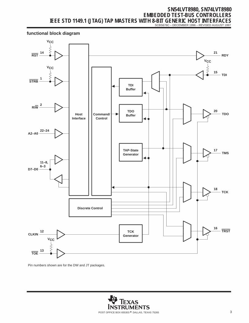
The eTBC masters all TAP signals required to support one 4- or 5-wire IEEE Std 1149.1 serial test bus – testclock (TCK), test mode select (TMS), test data input (TDI), test data output (TDO), and test reset (TRST). Allsuch signals can be connected directly to the associated target IEEE Std 1149.1 devices without need foradditional logic or buffering. However, as well as being directly connected, the TMS, TDI, and TDO signals canbe connected to distant target IEEE Std 1149.1 devices via a pipeline, with a retiming delay of up to 15 TCKcycles; the eTBC automatically handles all associated serial-data justification.
Conceptually, the eTBC operates as a simple 8-bit memory- or I/O- mapped peripheral to amicroprocessor/microcontroller (host). High-level commands and parallel data are passed to/from the eTBC viaits generic host interface, which includes an 8-bit data bus (D7–D0) and a 3-bit address bus (A2–A0). Read/writeselect (R/W) and strobe (STRB) signals are implemented so that the critical host-interface timing is independentof the CLKIN period. An asynchronous ready (RDY) indicator is provided to hold off, or insert wait states into,a host read/write cycle when the eTBC cannot respond immediately to the requested read/write operation.
High-level commands are issued by the host to cause the eTBC to generate the TMS sequences necessaryto move the test bus from any stable TAP-controller state to any other such stable state, to scan instruction ordata through test registers in target devices, and/or to execute instructions in the Run-Test/Idle TAP state. A32-bit counter can be programmed to allow a predetermined number of scan or execute cycles.
During scan operations, serial data that appears at the TDI input is transferred into a serial-to-4 × 8-bit-parallelfirst-in/first-out (FIFO) read buffer, which can then be read by the host to obtain the return serial-data streamup to eight bits at a time. Serial data that is to be transmitted from the TDO output is written by the host, up toeight bits at a time, to a 4 × 8-bit-parallel-to-serial FIFO write buffer.
In addition to such simple state-movement, scan, and run-test operations, the eTBC supports several additionalcommands that provide for input-only scans, output-only scans, recirculate scans (in which TDI is mirrored backto TDO), and a scan mode that generates the protocols used to support multidrop TAP configurations using TI’saddressable scan port. Two loopback modes also are supported that allow the microprocessor/microcontrollerhost to monitor the TDO or TMS data streams output by the eTBC.
The eTBC’s flexible clocking architecture allows the user to choose between free-running (in which the TCKalways follows CLKIN) and gated modes (in which the TCK output is held static except during state-move,run-test, or scan cycles) as well as to divide down TCK from CLKIN. A discrete mode is also available in whichthe TAP is driven strictly by read/write cycles under full control of the microprocessor/microcontroller host.These features ensure that virtually any IEEE Std 1149.1 target device or device chain – even where such maynot fully comply to IEEE Std 1149.1 – can be serviced by the eTBC.
While most operations of the eTBC are synchronous to CLKIN, a test-output enable (TOE) is provided for outputcontrol of the TAP outputs, and a reset (RST) input is provided for hardware reset of the eTBC. The former canbe used to disable the eTBC so that an external controller can master the associated IEEE Std 1149.1 test bus.
The SN54LVT8980 is characterized for operation over the full military temperature range of –55°C to 125°C.The SN74LVT8980 is characterized for operation from –40°C to 85°C.
SN54LVT8980, SN74LVT8980EMBEDDED TEST-BUS CONTROLLERS
IEEE STD 1149.1 (JTAG) TAP MASTERS WITH 8-BIT GENERIC HOST INTERFACES
SCBS676C – DECEMBER 1996 – REVISED AUGUST 1997
3POST OFFICE BOX 655303 • DALLAS, TEXAS 75265
functional block diagram
TDI
STRB
Discrete Control
A2–A0
R/W
D7–D0
RDYRST
VCC
CLKIN
TOE
TDO
TMS
TCK
TRSTTCKGenerator
HostInterface
Command/Control
TAP-StateGenerator
TDOBuffer
TDIBuffer
Pin numbers shown are for the DW and JT packages.
21
15
20
17
18
16
14
1
2
22–24
11–8,
12
13
6–3
VCC
VCC
VCC
SN54LVT8980, SN74LVT8980EMBEDDED TEST-BUS CONTROLLERSIEEE STD 1149.1 (JTAG) TAP MASTERS WITH 8-BIT GENERIC HOST INTERFACES
SCBS676C – DECEMBER 1996 – REVISED AUGUST 1997
4 POST OFFICE BOX 655303 • DALLAS, TEXAS 75265
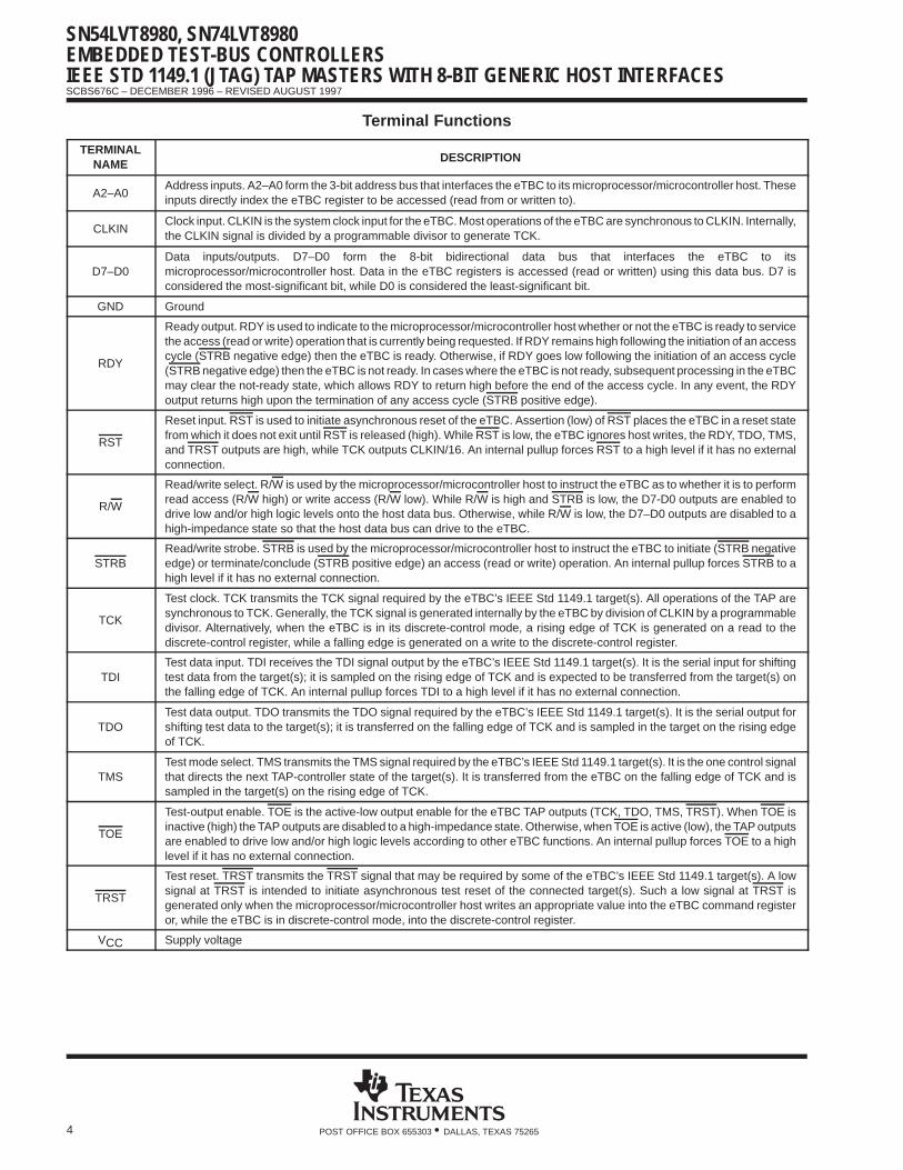
Terminal Functions
TERMINALNAME DESCRIPTION
A2–A0Address inputs. A2–A0 form the 3-bit address bus that interfaces the eTBC to its microprocessor/microcontroller host. Theseinputs directly index the eTBC register to be accessed (read from or written to).
CLKINClock input. CLKIN is the system clock input for the eTBC. Most operations of the eTBC are synchronous to CLKIN. Internally,the CLKIN signal is divided by a programmable divisor to generate TCK.
D7–D0Data inputs/outputs. D7–D0 form the 8-bit bidirectional data bus that interfaces the eTBC to itsmicroprocessor/microcontroller host. Data in the eTBC registers is accessed (read or written) using this data bus. D7 isconsidered the most-significant bit, while D0 is considered the least-significant bit.
GND Ground
RDY
Ready output. RDY is used to indicate to the microprocessor/microcontroller host whether or not the eTBC is ready to servicethe access (read or write) operation that is currently being requested. If RDY remains high following the initiation of an accesscycle (STRB negative edge) then the eTBC is ready. Otherwise, if RDY goes low following the initiation of an access cycle(STRB negative edge) then the eTBC is not ready. In cases where the eTBC is not ready, subsequent processing in the eTBCmay clear the not-ready state, which allows RDY to return high before the end of the access cycle. In any event, the RDYoutput returns high upon the termination of any access cycle (STRB positive edge).
RST
Reset input. RST is used to initiate asynchronous reset of the eTBC. Assertion (low) of RST places the eTBC in a reset statefrom which it does not exit until RST is released (high). While RST is low, the eTBC ignores host writes, the RDY, TDO, TMS,and TRST outputs are high, while TCK outputs CLKIN/16. An internal pullup forces RST to a high level if it has no externalconnection.
R/W
Read/write select. R/W is used by the microprocessor/microcontroller host to instruct the eTBC as to whether it is to performread access (R/W high) or write access (R/W low). While R/W is high and STRB is low, the D7-D0 outputs are enabled todrive low and/or high logic levels onto the host data bus. Otherwise, while R/W is low, the D7–D0 outputs are disabled to ahigh-impedance state so that the host data bus can drive to the eTBC.
STRBRead/write strobe. STRB is used by the microprocessor/microcontroller host to instruct the eTBC to initiate (STRB negativeedge) or terminate/conclude (STRB positive edge) an access (read or write) operation. An internal pullup forces STRB to ahigh level if it has no external connection.
TCK
Test clock. TCK transmits the TCK signal required by the eTBC’s IEEE Std 1149.1 target(s). All operations of the TAP aresynchronous to TCK. Generally, the TCK signal is generated internally by the eTBC by division of CLKIN by a programmabledivisor. Alternatively, when the eTBC is in its discrete-control mode, a rising edge of TCK is generated on a read to thediscrete-control register, while a falling edge is generated on a write to the discrete-control register.
TDITest data input. TDI receives the TDI signal output by the eTBC’s IEEE Std 1149.1 target(s). It is the serial input for shiftingtest data from the target(s); it is sampled on the rising edge of TCK and is expected to be transferred from the target(s) onthe falling edge of TCK. An internal pullup forces TDI to a high level if it has no external connection.
TDOTest data output. TDO transmits the TDO signal required by the eTBC’s IEEE Std 1149.1 target(s). It is the serial output forshifting test data to the target(s); it is transferred on the falling edge of TCK and is sampled in the target on the rising edgeof TCK.
TMSTest mode select. TMS transmits the TMS signal required by the eTBC’s IEEE Std 1149.1 target(s). It is the one control signalthat directs the next TAP-controller state of the target(s). It is transferred from the eTBC on the falling edge of TCK and issampled in the target(s) on the rising edge of TCK.
TOE
Test-output enable. TOE is the active-low output enable for the eTBC TAP outputs (TCK, TDO, TMS, TRST). When TOE isinactive (high) the TAP outputs are disabled to a high-impedance state. Otherwise, when TOE is active (low), the TAP outputsare enabled to drive low and/or high logic levels according to other eTBC functions. An internal pullup forces TOE to a highlevel if it has no external connection.
TRST
Test reset. TRST transmits the TRST signal that may be required by some of the eTBC’s IEEE Std 1149.1 target(s). A lowsignal at TRST is intended to initiate asynchronous test reset of the connected target(s). Such a low signal at TRST isgenerated only when the microprocessor/microcontroller host writes an appropriate value into the eTBC command registeror, while the eTBC is in discrete-control mode, into the discrete-control register.
VCC Supply voltage
SN54LVT8980, SN74LVT8980EMBEDDED TEST-BUS CONTROLLERS
IEEE STD 1149.1 (JTAG) TAP MASTERS WITH 8-BIT GENERIC HOST INTERFACES
SCBS676C – DECEMBER 1996 – REVISED AUGUST 1997
5POST OFFICE BOX 655303 • DALLAS, TEXAS 75265
application information
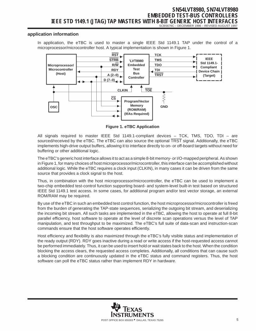
In application, the eTBC is used to master a single IEEE Std 1149.1 TAP under the control of amicroprocessor/microcontroller host. A typical implementation is shown in Figure 1.
IEEEStd 1149.1-Compliant
Device Chain(Target)TRST
RST
STRB
R/W
RDY
A (2–0)
D (7–0)
TDI
TDO
TMS
TCK
’LVT8980Embedded
TestBus
Controller
Microprocessor/Microcontroller
(Host)
Program/VectorMemory
(ROM/RAM)(If/As Required)
OSC
CLKIN TOE
CS
GND
Figure 1. eTBC Application
All signals required to master IEEE Std 1149.1-compliant devices – TCK, TMS, TDO, TDI – aresourced/received by the eTBC. The eTBC can also source the optional TRST signal. Additionally, the eTBCimplements high-drive output buffers, allowing it to interface directly to on- or off-board targets without need forbuffering or other additional logic.
The eTBC’s generic host interface allows it to act as a simple 8-bit memory- or I/O-mapped peripheral. As shownin Figure 1, for many choices of host microprocessor/microcontroller, this interface can be accomplished withoutadditional logic. While the eTBC requires a clock input (CLKIN), in many cases it can be driven from the samesource that provides a clock signal to the host.
Thus, in combination with the host microprocessor/microcontroller, the eTBC can be used to implement atwo-chip embedded test-control function supporting board- and system-level built-in test based on structuredIEEE Std 1149.1 test access. In some cases, for additional program and/or test vector storage, an externalROM/RAM may be required.
By use of the eTBC in such an embedded test control function, the host microprocessor/microcontroller is freedfrom the burden of generating the TAP-state sequences, serializing the outgoing bit stream, and deserializingthe incoming bit stream. All such tasks are implemented in the eTBC, allowing the host to operate at full 8-bitparallel efficiency, host software to operate at the level of discrete scan operations versus the level of TAPmanipulation, and test throughput to be maximized. The eTBC’s full suite of data-scan and instruction-scancommands ensure that the host software operates efficiently.
Host efficiency and flexibility is also maximized through the eTBC’s fully visible status and implementation ofthe ready output (RDY). RDY goes inactive during a read or write access if the host-requested access cannotbe performed immediately. Thus, it can be used to insert hold or wait states back to the host. When the conditionblocking the access clears, the requested access completes. Additionally, all conditions that can cause sucha blocking condition are continuously updated in the eTBC status and command registers. Thus, the hostsoftware can poll the eTBC status rather than implement RDY in hardware.
SN54LVT8980, SN74LVT8980EMBEDDED TEST-BUS CONTROLLERSIEEE STD 1149.1 (JTAG) TAP MASTERS WITH 8-BIT GENERIC HOST INTERFACES
SCBS676C – DECEMBER 1996 – REVISED AUGUST 1997
6 POST OFFICE BOX 655303 • DALLAS, TEXAS 75265
application information (continued)
The eTBC also provides several capabilities that support special target application requirements. The eTBC’stest-output enable allows its master function to be disabled so that another device (an external tester, forexample) can control the target TAP. Where required, due to target non-compliance or sensitivity to statesequencing, discrete-control mode provides the host software with arbitrary control of TMS and TDOsequences. Also, where targets may be sensitive to leaving Shift-DR state during scan operation, gated-TCKmode allows the TCK output to be stopped, rather than cycling the target TAP state to Pause-DR state, whenservice to TDI buffer or TDO buffer is required.
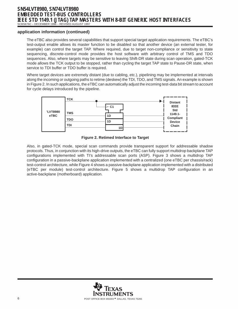
Where target devices are extremely distant (due to cabling, etc.), pipelining may be implemented at intervalsalong the incoming or outgoing paths to retime (deskew) the TDI, TDO, and TMS signals. An example is shownin Figure 2. In such applications, the eTBC can automatically adjust the incoming test-data bit stream to accountfor cycle delays introduced by the pipeline.
TDI
TDO
TMS
TCK
’LVT8980eTBC 1D
1D
1D
C1DistantIEEEStd
1149.1-Compliant
DeviceChain
Figure 2. Retimed Interface to Target
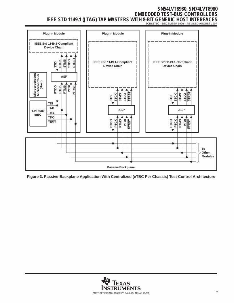
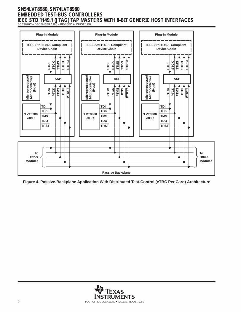
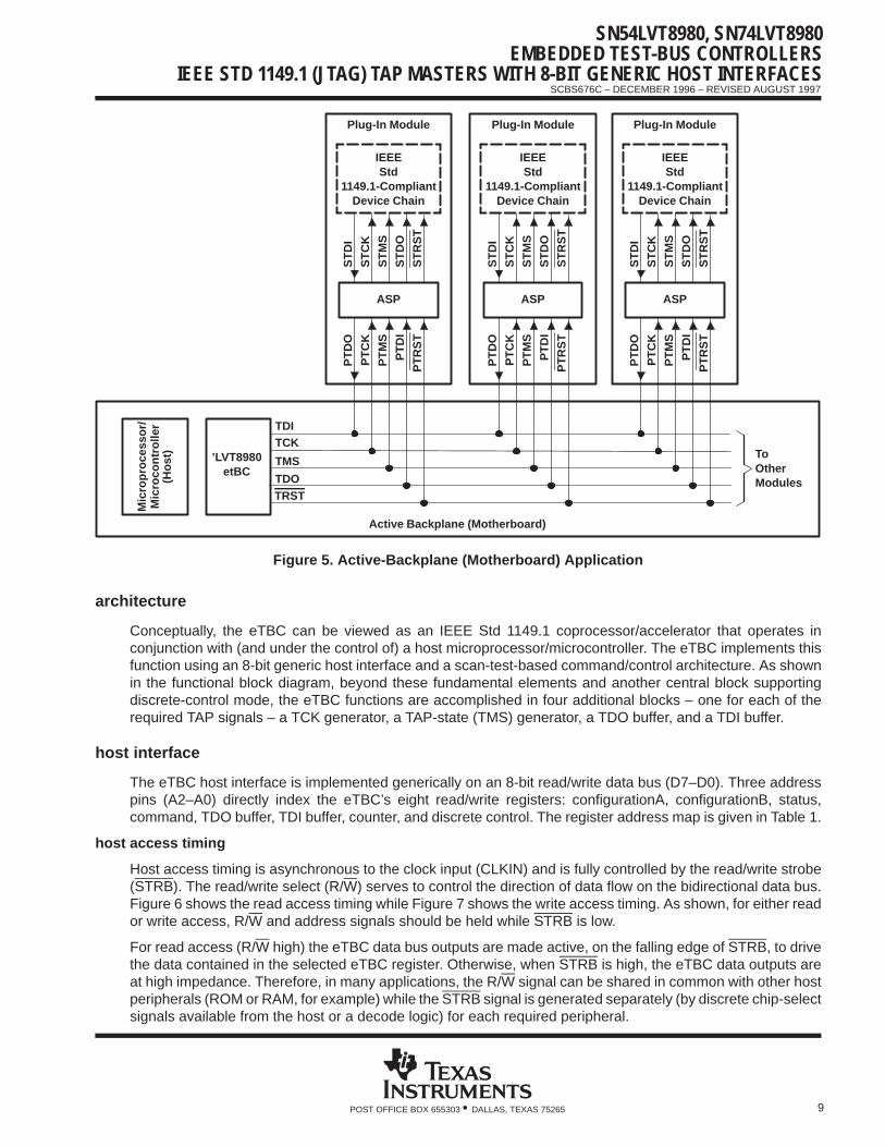
Also, in gated-TCK mode, special scan commands provide transparent support for addressable shadowprotocols. Thus, in conjunction with its high-drive outputs, the eTBC can fully support multidrop backplane TAPconfigurations implemented with TI’s addressable scan ports (ASP). Figure 3 shows a multidrop TAPconfiguration in a passive-backplane application implemented with a centralized (one eTBC per chassis/rack)test-control architecture, while Figure 4 shows a passive-backplane application implemented with a distributed(eTBC per module) test-control architecture. Figure 5 shows a multidrop TAP configuration in anactive-backplane (motherboard) application.
SN54LVT8980, SN74LVT8980EMBEDDED TEST-BUS CONTROLLERS
IEEE STD 1149.1 (JTAG) TAP MASTERS WITH 8-BIT GENERIC HOST INTERFACES
SCBS676C – DECEMBER 1996 – REVISED AUGUST 1997
7POST OFFICE BOX 655303 • DALLAS, TEXAS 75265
IEEE Std 1149.1-CompliantDevice Chain
PT
RS
T
PT
DI
PT
MS
PT
CK
PT
DO
ST
RS
T
ST
DO
ST
MS
ST
CK
ST
DI
TDO
TMS
TCKTDI
Plug-In Module
ToOtherModules
Passive Backplane
PT
RS
T
PT
DI
PT
MS
PT
CK
PT
DO
ST
RS
T
ST
DO
ST
MS
ST
CK
ST
DI
IEEE Std 1149.1-CompliantDevice Chain
Plug-In Module
IEEE Std 1149.1-CompliantDevice Chain
Plug-In Module
ASP
TRST
’LVT8980etBC
Mic
ropr
oces
sor/
Mic
roco
ntro
ller
(Hos
t)
ASP
PT
RS
T
PT
DI
PT
MS
PT
CK
PT
DO
ST
RS
T
ST
DO
ST
MS
ST
CK
ST
DI
ASP
Figure 3. Passive-Backplane Application With Centralized (eTBC Per Chassis) Test-Control Architecture
SN54LVT8980, SN74LVT8980EMBEDDED TEST-BUS CONTROLLERSIEEE STD 1149.1 (JTAG) TAP MASTERS WITH 8-BIT GENERIC HOST INTERFACES
SCBS676C – DECEMBER 1996 – REVISED AUGUST 1997
8 POST OFFICE BOX 655303 • DALLAS, TEXAS 75265
IEEE Std 1149.1-CompliantDevice Chain
PT
RS
T
PT
DI
PT
MS
PT
CK
PT
DO
ST
RS
T
ST
DO
ST
MS
ST
CK
ST
DI
TDO
TMS
TCKTDI
Plug-In Module
ToOtherModules
ASP
TRST
’LVT8980etBC
Mic
ropr
oces
sor/
Mic
roco
ntro
ller
(Hos
t)
Passive Backplane
IEEE Std 1149.1-CompliantDevice Chain
PT
RS
T
PT
DI
PT
MS
PT
CK
PT
DO
ST
RS
T
ST
DO
ST
MS
ST
CK
ST
DI
TDO
TMS
TCKTDI
Plug-In Module
ASP
TRST
’LVT8980etBC
Mic
ropr
oces
sor/
Mic
roco
ntro
ller
(Hos
t)
IEEE Std 1149.1-CompliantDevice Chain
PT
RS
T
PT
DI
PT
MS
PT
CK
PT
DO
ST
RS
T
ST
DO
ST
MS
ST
CK
ST
DI
TDO
TMS
TCKTDI
Plug-In Module
ASP
TRST
’LVT8980etBC
Mic
ropr
oces
sor/
Mic
roco
ntro
ller
(Hos
t)
ToOther
Modules
Figure 4. Passive-Backplane Application With Distributed Test-Control (eTBC Per Card) Architecture
SN54LVT8980, SN74LVT8980EMBEDDED TEST-BUS CONTROLLERS
IEEE STD 1149.1 (JTAG) TAP MASTERS WITH 8-BIT GENERIC HOST INTERFACES
SCBS676C – DECEMBER 1996 – REVISED AUGUST 1997
9POST OFFICE BOX 655303 • DALLAS, TEXAS 75265
TDO
TMS
TCKTDI
ToOtherModules
Active Backplane (Motherboard)
PT
RS
T
PT
DI
PT
MS
PT
CK
PT
DO
ST
RS
T
ST
DO
ST
MS
ST
CK
ST
DI
Plug-In Module
’LVT8980etBC
Mic
ropr
oces
sor/
Mic
roco
ntro
ller
(Hos
t)
ASP
IEEEStd
1149.1-CompliantDevice Chain
TRST
PT
RS
T
PT
DI
PT
MS
PT
CK
PT
DO
ST
RS
T
ST
DO
ST
MS
ST
CK
ST
DI
Plug-In Module
ASP
IEEEStd
1149.1-CompliantDevice Chain
PT
RS
T
PT
DI
PT
MS
PT
CK
PT
DO
ST
RS
T
ST
DO
ST
MS
ST
CK
ST
DI
Plug-In Module
ASP
IEEEStd
1149.1-CompliantDevice Chain
Figure 5. Active-Backplane (Motherboard) Application
architecture
Conceptually, the eTBC can be viewed as an IEEE Std 1149.1 coprocessor/accelerator that operates inconjunction with (and under the control of) a host microprocessor/microcontroller. The eTBC implements thisfunction using an 8-bit generic host interface and a scan-test-based command/control architecture. As shownin the functional block diagram, beyond these fundamental elements and another central block supportingdiscrete-control mode, the eTBC functions are accomplished in four additional blocks – one for each of therequired TAP signals – a TCK generator, a TAP-state (TMS) generator, a TDO buffer, and a TDI buffer.
host interface
The eTBC host interface is implemented generically on an 8-bit read/write data bus (D7–D0). Three addresspins (A2–A0) directly index the eTBC’s eight read/write registers: configurationA, configurationB, status,command, TDO buffer, TDI buffer, counter, and discrete control. The register address map is given in Table 1.
host access timing
Host access timing is asynchronous to the clock input (CLKIN) and is fully controlled by the read/write strobe(STRB). The read/write select (R/W) serves to control the direction of data flow on the bidirectional data bus.Figure 6 shows the read access timing while Figure 7 shows the write access timing. As shown, for either reador write access, R/W and address signals should be held while STRB is low.
For read access (R/W high) the eTBC data bus outputs are made active, on the falling edge of STRB, to drivethe data contained in the selected eTBC register. Otherwise, when STRB is high, the eTBC data outputs areat high impedance. Therefore, in many applications, the R/W signal can be shared in common with other hostperipherals (ROM or RAM, for example) while the STRB signal is generated separately (by discrete chip-selectsignals available from the host or a decode logic) for each required peripheral.

SN54LVT8980, SN74LVT8980EMBEDDED TEST-BUS CONTROLLERSIEEE STD 1149.1 (JTAG) TAP MASTERS WITH 8-BIT GENERIC HOST INTERFACES
SCBS676C – DECEMBER 1996 – REVISED AUGUST 1997
10 POST OFFICE BOX 655303 • DALLAS, TEXAS 75265
host access timing (continued)
For write access (R/W low), the eTBC data outputs remain at high impedance independent of STRB. Theaddress of the register to be written is latched from the address pins on the falling edge of STRB, while the datato be written is latched from the data bus on the rising edge of STRB.
tPHL
th
th
STRB
RDY
R/W
D
A
tsu
tsu
Valid
tPLH
tPZH or t PZL tPHZ or t PLZ
Figure 6. Read Access Timing
th
tPHL
th
th
STRB
RDY
R/W
D
A
tsu
tsu
Valid
tPLH
tsu
Valid
Figure 7. Write Access Timing

SN54LVT8980, SN74LVT8980EMBEDDED TEST-BUS CONTROLLERS
IEEE STD 1149.1 (JTAG) TAP MASTERS WITH 8-BIT GENERIC HOST INTERFACES
SCBS676C – DECEMBER 1996 – REVISED AUGUST 1997
11POST OFFICE BOX 655303 • DALLAS, TEXAS 75265
ready output
The ready output (RDY) from the host interface can be used, where the selected microprocessor/microcontrollersupports it, to insert wait or hold states back to the host. If a host-requested access cannot be performedimmediately, RDY goes inactive (low) during that given access. When the condition blocking the access clears,RDY goes active (high) and the eTBC grants the requested access. Alternatively, where suchhardware-generated hold or wait states are not supported in the selected microprocessor/microcontroller host,the eTBC status and/or command registers can be polled to determine its readiness to grant a given read orwrite access.
Conditions that cause a host access to be blocked (and RDY to become inactive) are limited to the following:
While the TDI buffer is empty, as indicated in status register (bit 7, TDIS), a requested read to TDI-bufferregister generates RDY inactive; this condition clears, RDY goes active, and the requested accesscompletes, when the TDI buffer is no longer empty.
While the TDO buffer is full or is being reset upon initiation of a scan command, as indicated in status register(bit 6, TDOS), a requested write to TDO-buffer register generates RDY inactive; this condition clears, RDYgoes active, and the requested access completes, when the TDO buffer is no longer full or the TDO-bufferreset completes, as applicable.
While a command is in progress, as indicated by a non-zero value in the opcode field (bits 3–0, OPCOD)of the command register, a requested write to command, configurationA, configurationB, or counterregisters generates RDY inactive. This condition clears, RDY goes active, and the requested access iscomplete, when the previously specified command finishes. The sole exception is the writing of a logic 1into the software reset (bit 7, SWRST) bit of the command register, which is never blocked.
While a full-duplex scan command is in progress, and the number of retiming-delay bits is other than zero,the number of writes to TDO-buffer register may not exceed, by more than 5, the number of reads toTDI-buffer register. A write to TDO-buffer register that does exceed this limit is blocked, and generates RDYinactive, indefinitely; the TDI-buffer register must be read before another write to TDO-buffer register.
SN54LVT8980, SN74LVT8980EMBEDDED TEST-BUS CONTROLLERSIEEE STD 1149.1 (JTAG) TAP MASTERS WITH 8-BIT GENERIC HOST INTERFACES
SCBS676C – DECEMBER 1996 – REVISED AUGUST 1997
12 POST OFFICE BOX 655303 • DALLAS, TEXAS 75265
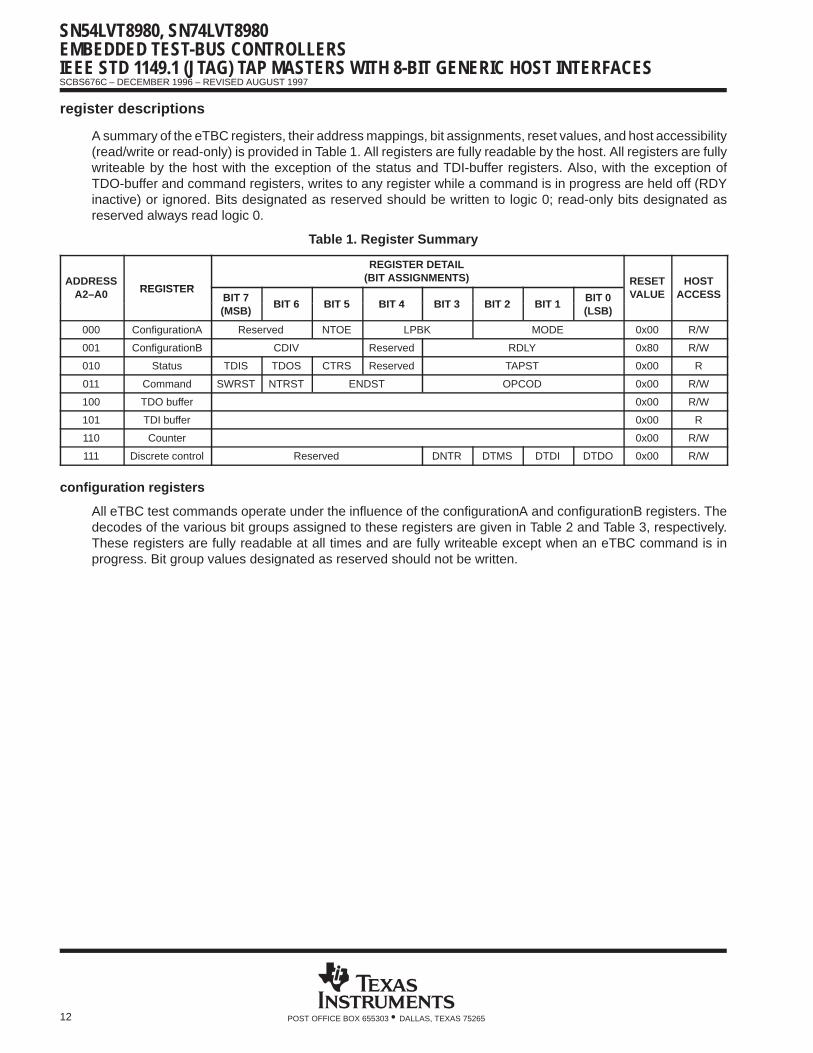
register descriptions
A summary of the eTBC registers, their address mappings, bit assignments, reset values, and host accessibility(read/write or read-only) is provided in Table 1. All registers are fully readable by the host. All registers are fullywriteable by the host with the exception of the status and TDI-buffer registers. Also, with the exception ofTDO-buffer and command registers, writes to any register while a command is in progress are held off (RDYinactive) or ignored. Bits designated as reserved should be written to logic 0; read-only bits designated asreserved always read logic 0.
Table 1. Register Summary
ADDRESSREGISTER
REGISTER DETAIL(BIT ASSIGNMENTS) RESET HOST
A2–A0 REGISTERBIT 7
BIT 6 BIT 5 BIT 4 BIT 3 BIT 2 BIT 1BIT 0 VALUE ACCESS
(MSB)BIT 6 BIT 5 BIT 4 BIT 3 BIT 2 BIT 1
(LSB)
000 ConfigurationA Reserved NTOE LPBK MODE 0x00 R/W
001 ConfigurationB CDIV Reserved RDLY 0x80 R/W
010 Status TDIS TDOS CTRS Reserved TAPST 0x00 R
011 Command SWRST NTRST ENDST OPCOD 0x00 R/W
100 TDO buffer 0x00 R/W
101 TDI buffer 0x00 R
110 Counter 0x00 R/W
111 Discrete control Reserved DNTR DTMS DTDI DTDO 0x00 R/W
configuration registers
All eTBC test commands operate under the influence of the configurationA and configurationB registers. Thedecodes of the various bit groups assigned to these registers are given in Table 2 and Table 3, respectively.These registers are fully readable at all times and are fully writeable except when an eTBC command is inprogress. Bit group values designated as reserved should not be written.

SN54LVT8980, SN74LVT8980EMBEDDED TEST-BUS CONTROLLERS
IEEE STD 1149.1 (JTAG) TAP MASTERS WITH 8-BIT GENERIC HOST INTERFACES
SCBS676C – DECEMBER 1996 – REVISED AUGUST 1997
13POST OFFICE BOX 655303 • DALLAS, TEXAS 75265
Table 2. ConfigurationA Register Decode
CONFIGURATIONA
BITGROUP BIT NO.
VALUE RESULT
NTOE 50 TAP outputs (TCK, TDO, TMS, TRST) are enabled.
NTOE 51 TAP outputs (TCK, TDO, TMS, TRST) are disabled (high impedance).
00 No loopback – TDI pin inputs to TDI buffer.
LPBK 4 301 TMS loopback – TAP-state generator inputs to TDI buffer. TMS and TDO pins are fixed high.
LPBK 4–310 TDO loopback – TDO buffer inputs to TDI buffer. TMS and TDO pins are fixed high.
11 Reserved
000
Automatic/free-running-TCK mode – all TAP outputs are generated autonomously in the eTBC accordingto the active command. The TCK output runs continuously; while operating a scan command, if the TDIbuffer becomes full and/or the TDO buffer becomes empty, the TAP state is cycled to Pause-DR orPause-IR, as appropriate, until the host performs the required buffer service.
MODE 2–0 001
Automatic/gated-TCK mode – all TAP outputs are generated autonomously in the eTBC according to theactive command. The TCK output is run only when required to move TAP state or to progress run-test orscan operations, otherwise, it is gated off (low); while operating a scan command, if the TDI bufferbecomes full and/or the TDO buffer becomes empty, the TAP state remains in Shift-IR or Shift-DR, asappropriate, but the TCK output is gated off until the host performs the required buffer service.
010Discrete-control mode – all TAP outputs are determined by contents of the discrete-control register undercontrol of host software.
011–111 Reserved
Table 3. ConfigurationB Register Decode
CONFIGURATIONB
BITGROUP BIT NO.
VALUE RESULT
CDIV 7–5 000–111 TCK = (CLKIN)/(2CDIV); reset value TCK = (CLKIN)/(24) = CLKIN/16
RDLY 3–00000–11
11
Number of retiming delays to accommodate = RDLY; while operating a scan command, TDI sampling isdelayed by a number of TCK cycles, equal to RDLY, following the generation of Shift-DR or Shift-IR state,as appropriate.
The negated test-output-enable (NTOE) bit allows the host to disable the TAP outputs via software in a manneranalogous to the hardware TOE. The loopback (LPBK) bit group allows the selection of the source of data tobe input to the TDI buffer – from the TDI pin for normal eTBC operations or, for eTBC verification purpose, fromTAP-state (TMS) generator or TDO buffer. The test mode (MODE) bit group provides a choice ofautomatic/free-running-TCK, automatic/gated-TCK, or discrete-control modes.
The clock-divisor (CDIV) bit group allows software control of the TCK output frequency based on a division ofthe CLKIN input. Divisors from 20 (1) to 27 (128) are provided. The clock divisor defaults to 24 (16) on eTBCreset (power-up, hardware-initiated, or software-initiated). The retiming-delay (RDLY) bit group provides for theautomatic accommodation of retiming (pipeline) delays, which can be used to deskew the TAP signals to targetscan chains that are electrically distant (due to cabling delays, etc).

SN54LVT8980, SN74LVT8980EMBEDDED TEST-BUS CONTROLLERSIEEE STD 1149.1 (JTAG) TAP MASTERS WITH 8-BIT GENERIC HOST INTERFACES
SCBS676C – DECEMBER 1996 – REVISED AUGUST 1997
14 POST OFFICE BOX 655303 • DALLAS, TEXAS 75265
status register
The status of the eTBC is fully reported and continuously updated in the status register. The decode of thevarious bit groups assigned to the status register is given in Table 4.
Table 4. Status Register Decode
STATUS
BITGROUP BIT NO.
VALUE RESULT
TDIS 70 The TDI buffer is empty – no TDI data is available for host read.
TDIS 71 The TDI buffer is not empty – at least one byte of TDI data is available for host read.
TDOS 60 The TDO buffer is not full – at least one byte in TDO buffer is available for host write.
TDOS 61 The TDO buffer is full – no bytes in TDO buffer are available for host write.
CTRS 50
The counter is not loaded with a complete 32-bit value – command operation cannot begin until counterload completes.
1 The counter is loaded with a complete 32-bit value – command operation can begin.
0000 The current target TAP state (as sent by eTBC) is Test-Logic-Reset.
0001 The current target TAP state (as sent by eTBC) is Select-DR-Scan.
0010 The current target TAP state (as sent by eTBC) is Capture-DR.
0011 The current target TAP state (as sent by eTBC) is Shift-DR.
0100 The current target TAP state (as sent by eTBC) is Exit1-DR.
0101 The current target TAP state (as sent by eTBC) is Pause-DR.
0110 The current target TAP state (as sent by eTBC) is Exit2-DR.
TAPST 3 00111 The current target TAP state (as sent by eTBC) is Update-DR.
TAPST 3–01000 The current target TAP state (as sent by eTBC) is Run-Test/Idle.
1001 The current target TAP state (as sent by eTBC) is Select-IR-Scan.
1010 The current target TAP state (as sent by eTBC) is Capture-IR.
1011 The current target TAP state (as sent by eTBC) is Shift-IR
1100 The current target TAP state (as sent by eTBC) is Exit1-IR.
1101 The current target TAP state (as sent by eTBC) is Pause-IR.
1110 The current target TAP state (as sent by eTBC) is Exit2-IR.
1111 The current target TAP state (as sent by eTBC) is Update-IR.
The TDI-buffer-status (TDIS) bit reports the readiness of the TDI buffer to respond to a host read. TheTDO-buffer-status (TDOS) bit reports the readiness of the TDO buffer to respond to a host write. Thecounter-status (CTRS) bit reports the readiness of the counter to support a command that uses the counter. Thecurrent-TAP-state (TAPST) bit group continuously reports the target TAP state as monitored by the eTBC.
command register
The command register is used to perform software reset of the eTBC, to discretely control the state of the TRSToutput when not in discrete-control mode, and to initiate test operations in the target(s).The decode of thevarious bits assigned to the command register is given in Table 5.
Any read to the command register while a command is in progress returns the value written to the commandregister upon initiation of the command. Once a command finishes, the operation-code (OPCOD) bit group inthe command register is reset to null. In this way, the status of a requested command can be monitored/polledby the host.
With the exception of the software-reset (SWRST) bit, which can be written at any time, writes to the commandregister while a command is in progress causes RDY inactive and is ignored if the write cycle is terminatedbefore the previously requested command finishes.
SN54LVT8980, SN74LVT8980EMBEDDED TEST-BUS CONTROLLERS
IEEE STD 1149.1 (JTAG) TAP MASTERS WITH 8-BIT GENERIC HOST INTERFACES
SCBS676C – DECEMBER 1996 – REVISED AUGUST 1997
15POST OFFICE BOX 655303 • DALLAS, TEXAS 75265
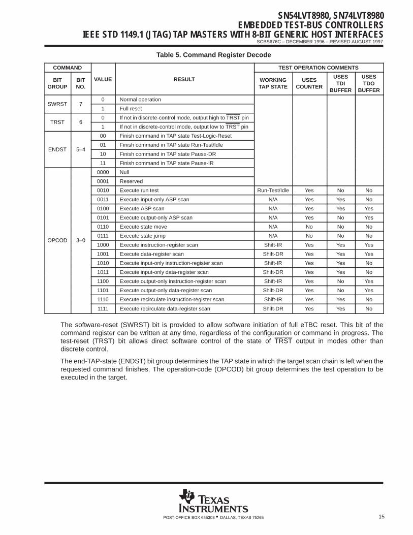
Table 5. Command Register Decode
COMMAND TEST OPERATION COMMENTS
BITGROUP
BITNO.
VALUE RESULT WORKINGTAP STATE
USESCOUNTER
USESTDI
BUFFER
USESTDO
BUFFER
SWRST 70 Normal operation
SWRST 71 Full reset
TRST 60 If not in discrete-control mode, output high to TRST pin
TRST 61 If not in discrete-control mode, output low to TRST pin
00 Finish command in TAP state Test-Logic-Reset
ENDST 5 401 Finish command in TAP state Run-Test/Idle
ENDST 5–410 Finish command in TAP state Pause-DR
11 Finish command in TAP state Pause-IR
0000 Null
0001 Reserved
0010 Execute run test Run-Test/Idle Yes No No
0011 Execute input-only ASP scan N/A Yes Yes No
0100 Execute ASP scan N/A Yes Yes Yes
0101 Execute output-only ASP scan N/A Yes No Yes
0110 Execute state move N/A No No No
OPCOD 3 00111 Execute state jump N/A No No No
OPCOD 3–01000 Execute instruction-register scan Shift-IR Yes Yes Yes
1001 Execute data-register scan Shift-DR Yes Yes Yes
1010 Execute input-only instruction-register scan Shift-IR Yes Yes No
1011 Execute input-only data-register scan Shift-DR Yes Yes No
1100 Execute output-only instruction-register scan Shift-IR Yes No Yes
1101 Execute output-only data-register scan Shift-DR Yes No Yes
1110 Execute recirculate instruction-register scan Shift-IR Yes Yes No
1111 Execute recirculate data-register scan Shift-DR Yes Yes No
The software-reset (SWRST) bit is provided to allow software initiation of full eTBC reset. This bit of thecommand register can be written at any time, regardless of the configuration or command in progress. Thetest-reset (TRST) bit allows direct software control of the state of TRST output in modes other thandiscrete control.
The end-TAP-state (ENDST) bit group determines the TAP state in which the target scan chain is left when therequested command finishes. The operation-code (OPCOD) bit group determines the test operation to beexecuted in the target.
SN54LVT8980, SN74LVT8980EMBEDDED TEST-BUS CONTROLLERSIEEE STD 1149.1 (JTAG) TAP MASTERS WITH 8-BIT GENERIC HOST INTERFACES
SCBS676C – DECEMBER 1996 – REVISED AUGUST 1997
16 POST OFFICE BOX 655303 • DALLAS, TEXAS 75265
counter register
The counter register, while only 8 bits wide like any other eTBC register, provides read/write access to the full32-bit eTBC counter. Writes to the counter register are accomplished by four complete host access cycles,otherwise the counter is considered unloaded (CTRS = 0). Reads to the counter register likewise areaccomplished by four complete host access cycles. However, reads do not affect the counter-loaded status(CTRS). The counter access (both read and write) is in least-significant-byte-first order. Any writes to the counterregister while a command is in progress are ignored. The 32-bit value present in the counter at initiation of acommand is used to determine the number of TCK cycles or scan bits for which the command is operated.
TDO-buffer register
The TDO-buffer register, while only 8 bits wide like any other eTBC register, provides write access to the full4 × 8 (32-bit) FIFO that comprises the TDO buffer. The TDO-buffer register can be written as long as the TDObuffer does not become full. When the TDO buffer becomes full, further writes to the TDO-buffer register causeRDY inactive (and consequent hold or wait states to be sent back to the host, if supported) and cause the writeto be ignored if the write cycle is terminated before the TDO-buffer-full status is cleared.
TDI-buffer register
The TDI-buffer register, while only 8 bits wide like any other eTBC register, provides read access to the full 4 × 8(32-bit) FIFO that comprises the TDI buffer. The TDI-buffer register can be read as long as the TDI buffer doesnot become empty. When the TDI buffer becomes empty, further reads to the TDI-buffer register cause RDYinactive (and consequent hold or wait states to be sent back to the host, if supported) and cause the read datato be invalid if the read cycle is terminated before the TDI-buffer-empty status is cleared.
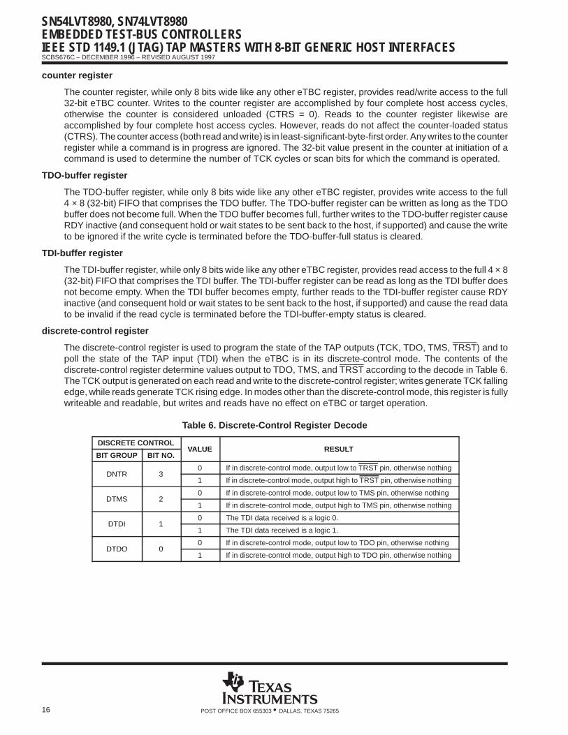
discrete-control register
The discrete-control register is used to program the state of the TAP outputs (TCK, TDO, TMS, TRST) and topoll the state of the TAP input (TDI) when the eTBC is in its discrete-control mode. The contents of thediscrete-control register determine values output to TDO, TMS, and TRST according to the decode in Table 6.The TCK output is generated on each read and write to the discrete-control register; writes generate TCK fallingedge, while reads generate TCK rising edge. In modes other than the discrete-control mode, this register is fullywriteable and readable, but writes and reads have no effect on eTBC or target operation.
Table 6. Discrete-Control Register Decode
DISCRETE CONTROLVALUE RESULT
BIT GROUP BIT NO.VALUE RESULT
DNTR 30 If in discrete-control mode, output low to TRST pin, otherwise nothing
DNTR 31 If in discrete-control mode, output high to TRST pin, otherwise nothing
DTMS 20 If in discrete-control mode, output low to TMS pin, otherwise nothing
DTMS 21 If in discrete-control mode, output high to TMS pin, otherwise nothing
DTDI 10 The TDI data received is a logic 0.
DTDI 11 The TDI data received is a logic 1.
DTDO 00 If in discrete-control mode, output low to TDO pin, otherwise nothing
DTDO 01 If in discrete-control mode, output high to TDO pin, otherwise nothing
SN54LVT8980, SN74LVT8980EMBEDDED TEST-BUS CONTROLLERS
IEEE STD 1149.1 (JTAG) TAP MASTERS WITH 8-BIT GENERIC HOST INTERFACES
SCBS676C – DECEMBER 1996 – REVISED AUGUST 1997
17POST OFFICE BOX 655303 • DALLAS, TEXAS 75265
command/control
The eTBC’s command-based architecture is structured around a set of comprehensive IEEE Std 1149.1 (JTAG)test objectives, which include TAP state movement, scan operations, and run test (operation of test logic inRun-Test/Idle state). The set of test operations, as decoded from the command register (bits 3–0, OPCOD) isgiven in Table 5. Commands are initiated by writing the eTBC command register; upon command initiation, thetest-control logic is initialized and the TDO and TDI buffers are cleared. Command completion is indicated whenthe operation code (OPCOD) field of the command register returns to the value of the null command.
The eTBC command operation is modified by the configurationA, and configurationB registers, which shouldbe written prior to writing the command register, as the values in these registers cannot be modified while acommand is in progress. Also, commands are only operated in automatic test modes, as specified in theconfigurationA register (bits 2–0, MODE) – while in the discrete-control mode, commands are ignored.
All eTBC commands operate similarly to accomplish IEEE Std 1149.1 test objectives. First, the eTBC generatesa TMS sequence to move the target scan chain from its current TAP state to a working state that depends onthe test objective. Second, the command is operated (test run, bits scanned) in the working state for a numberof TCK cycles (or scan bits) determined by the value of the counter upon command initiation. Third, the eTBCgenerates a TMS sequence to move the target scan chain from the working state to the end state specified inthe command register (bits 5–4, ENDST). For some commands, one or more of these steps are omitted.
TAP-state-movement commands
Two eTBC commands are provided to accomplish TAP state movement. The state-move command operatesto generate a TMS sequence to move the target scan chain directly from its current TAP state to the end statespecified in the command register. The state-jump command moves the eTBC’s stored value of the target TAPstate without generating any changes to the TMS output. The state-jump command can therefore be used toswitch between targets that share the same test bus, such as those in a multidrop backplane configurationimplemented with TI addressable scan ports, but that may be left in different TAP states.
run-test command
The run-test command allows the test logic of the target scan chain to execute autonomously in theRun-Test/Idle TAP state. Such test logic is commonly used to implement chip- or board-level built-in self test.The run-test command generates TMS sequences to move the target scan chain from its current TAP state tothe Run-Test/Idle TAP state where it remains for a number of TCK cycles determined by the value of the counterupon command initiation. Upon the countdown of the counter to zero, the eTBC generates TMS sequences tomove the target scan chain to the end state specified in the command register.
scan commands
Eleven eTBC commands are provided to perform scan operations to target scan chains. These can be classifiedby the destination of scan data in the target – addressable scan port (ASP), IEEE Std 1149.1 instruction register,or IEEE Std 1149.1 data register – and by the nature/direction of the data transfer – full-duplex (default),input-only, output-only, or recirculate. The only combination of these two factors that is not implemented isrecirculate ASP scan.
addressable scan port (ASP) scan commands
The ASP scan commands scan data to and/or from an addressable scan port target. Since ASP devices requirethat TMS remain fixed throughout their select and acknowledge protocols, the eTBC does not generate TMSsequences or change its stored value of the target’s TAP state. Also, for the same reason, ASP scan commandsthat target ASP devices should be operated in gated-TCK mode. The ASP scan commands do allow data writtento the TDO buffer to be driven serially onto the TDO pin and bits received serially at the TDI pin to be storedinto the TDI buffer for reading by the host. However, the ASP scan commands do not perform any bit-pairencoding of ASP select protocols or decoding of ASP acknowledge protocols. Such encoding/decoding mustbe performed in the host. The number of data bits transferred in and/or out is determined by the value of thecounter upon command initiation.
SN54LVT8980, SN74LVT8980EMBEDDED TEST-BUS CONTROLLERSIEEE STD 1149.1 (JTAG) TAP MASTERS WITH 8-BIT GENERIC HOST INTERFACES
SCBS676C – DECEMBER 1996 – REVISED AUGUST 1997
18 POST OFFICE BOX 655303 • DALLAS, TEXAS 75265
instruction-register scan commands
The instruction-register scan commands scan bits to and/or from the concatenation of instruction registers ina target scan chain. The eTBC generates a TMS sequence to move the target scan chain from its current TAPstate to the Shift-IR TAP state. Data written to the TDO buffer can be driven serially onto the TDO pin and bitsreceived serially at the TDI pin can be stored into the TDI buffer for reading by the host. The number of databits transferred in and/or out is determined by the value of the counter upon command initiation. If, during theoperation of an instruction register scan command, the TDO buffer becomes empty, or the TDI buffer becomesfull, the TAP state is sequenced to Pause-IR (if in free-running-TCK mode) or the TCK output is gated off (if ingated-TCK mode) until the required buffer service is performed. Upon the countdown of the counter to zero,the eTBC generates TMS sequences to move the target scan chain to the end state specified in the commandregister.
data-register scan commands
The data-register scan commands operate to scan bits to and/or from the concatenation of data registers in atarget scan chain. The eTBC generates a TMS sequence to move the target scan chain from its current TAPstate to the Shift-DR TAP state. Data written to the TDO buffer may be driven serially onto the TDO pin and bitsreceived serially at the TDI pin may be stored into the TDI buffer for reading by the host. The number of databits transferred in and/or out is determined by the value of the counter upon command initiation. If, during theoperation of a data-register scan command, the TDO buffer becomes empty, or the TDI buffer becomes full, theTAP state is sequenced to Pause-DR (if in free-running-TCK mode) or the TCK output is gated off (if ingated-TCK mode) until the required buffer service is performed. Upon the countdown of the counter to zero,the eTBC generates TMS sequences to move the target scan chain to the end state specified in thecommand register.
other scan-command variations
As noted before, the nature/direction of the data transfer for any scan command can vary along with thedestination of scan data in the target, as follows:
For scan commands of the full-duplex (default) class, both TDO buffer and TDI buffer are used to scan datato and from the target scan chain, respectively.
For scan commands of the input-only class, only the TDI buffer is used to scan data from the target scanchain; outgoing TDO data is fixed at a high level throughout the scan operation.
For scan commands of the output-only class, only the TDO buffer is used to scan data to the target scanchain; incoming TDI data is simply ignored.
For scan commands of the recirculate class, only the TDI buffer is used to scan data from the target scanchain; outgoing TDO data is generated by recirculating the incoming TDI data back into the targetscan chain.
counter
As described above, the value loaded in the eTBC’s 32-bit counter at initiation of a command is used to specifythe number of TCK cycles or scan bits to remain in the command’s working state. As each TCK cycle or scanbit is processed for a run-test or scan command, respectively, the counter value is decremented. When thecounter value reaches zero, the command leaves its working state to finish in the end state specified in thecommand register.
Before a command that uses the counter can be initiated, a full 32-bit value should be loaded by four consecutivewrites to the counter register. As well, the full 32-bit current value of the counter can be observed by fourconsecutive reads to the counter register. The counter status (unloaded/loaded) is maintained and observablein the status register (bit 5, CTRS).
Upon eTBC reset (power-up, hardware-initiated, or software-initiated), the counter is cleared and assumes itsunloaded state.
SN54LVT8980, SN74LVT8980EMBEDDED TEST-BUS CONTROLLERS
IEEE STD 1149.1 (JTAG) TAP MASTERS WITH 8-BIT GENERIC HOST INTERFACES
SCBS676C – DECEMBER 1996 – REVISED AUGUST 1997
19POST OFFICE BOX 655303 • DALLAS, TEXAS 75265
TCK generator
The TCK generator sources the test clock (TCK) signal required by the IEEE Std 1149.1 target(s) and theeTBC-internal test-control logic. The fundamental TCK frequency is produced by division of CLKIN. The divisoris programmable within a range of 1 to 128 in the configurationB register (bits 7–5, CDIV). The TCK output tothe target(s) operate in free-running or gated modes. The free-running mode toggles TCK continuously, basedon CLKIN, while the gated mode operates the TCK only when required to move the target TAP state or to performa run-test or scan operation.
While the eTBC is in discrete-control mode, the TCK generator is not used; instead, the state of TCK is toggledon each alternating read and write to the discrete-control register. A falling edge of TCK is produced by write,while a rising edge of TCK is produced by read.
Upon eTBC reset (power-up, hardware-initiated, or software-initiated), the TCK generator assumes itsfree-running mode with a clock divisor of 16 (TCK = CLKIN/16).
TAP-state generator
The TAP-state generator sources the TMS signal, which sequences the TAP controllers of connectedIEEE Std 1149.1-compliant target devices. The TAP controller specified by IEEE Std 1149.1 is a synchronousfinite-state machine that provides test control signals throughout each target device; its state diagram is shownin Figure 8. This diagram and the TAP-controller states are discussed subsequently.
The TAP-state generator operates under the control of an executing command to generate the TMS sequencesrequired to move connected target devices from one stable state to another, to capture and scan test datainto/out of target devices, and to operate built-in test modes of target devices in the Run-Test/Idle state.
The TAP state currently being generated is always maintained by the TAP-state generator and is constantlyavailable in the eTBC status register (bits 3–0, TAPST) for host read. Based on the TAP state that is current uponcommand initiation, the TAP-state generator will source a defined sequence of TMS values to reach the TAPstate in which the command is progressed (e.g., Shift-IR, Shift-DR, Run-Test/Idle), and ultimately to reach thespecified end TAP state. These sequences are detailed in Tables 7–12.
While the eTBC is in free-running-TCK mode, if a currently operating scan command empties or fills a requiredtest data buffer, then the TAP-state generator sources the TMS sequences required to move the connectedtarget devices to their Pause-IR or Pause-DR states. In such case, the TAP-state generator maintains targetdevices in their Pause-IR or Pause-DR states until the required test data buffer is serviced appropriately.However, if such a buffer condition occurs while the eTBC is in gated-TCK mode, the TAP-state generatormaintains the target devices in their Shift-IR or Shift-DR states while the TCK is gated off.
While the eTBC is in discrete-control mode, the TAP-state generator is not used; instead, the state of the TMSpin is determined by the contents of the discrete-control register. Thus, TMS sequences that cannot begenerated automatically still can be applied through the eTBC to targets that require such (e.g., near-compliantdevices).
The TAP-state generator also is not used during the operation of the special addressable shadow protocol(ASP) scan commands. Since, by definition, ASPs operate only while the TAP is idling (maintaining one of theTAP states Test-Logic-Reset, Run-Test/Idle, Pause-IR, or Pause-DR), the TMS pin must be maintained at thevalue it held upon initiation of the ASP scan command.
For eTBC verification/debugging, in addition to continuous update of the current target TAP state in the eTBCstatus register, the output of the TAP-state (TMS) generator can be selected for loopback into the TDI buffer.When this TMS-loopback mode is selected, although a host-requested command executes in the eTBC, thetarget is not affected, as both TMS and TDI are fixed at a high level.
Upon eTBC reset (power up, hardware initiated, or software initiated), the TAP-state generator assumes theTest-Logic-Reset TAP state.

SN54LVT8980, SN74LVT8980EMBEDDED TEST-BUS CONTROLLERSIEEE STD 1149.1 (JTAG) TAP MASTERS WITH 8-BIT GENERIC HOST INTERFACES
SCBS676C – DECEMBER 1996 – REVISED AUGUST 1997
20 POST OFFICE BOX 655303 • DALLAS, TEXAS 75265
Table 7. TMS Sequencing From TAP State Test-Logic-Reset
FROM TEST-LOGIC-RESET (TMS = H) TO:
TEST-LOGIC-RESET RUN-TEST-IDLE SHIFT-DR PAUSE-DR SHIFT-IR PAUSE-IR
NEXTTMS
NEXTTAP
STATE
NEXTTMS
NEXTTAP
STATE
NEXTTMS
NEXTTAP
STATE
NEXTTMS
NEXTTAP
STATE
NEXTTMS
NEXTTAP
STATE
NEXTTMS
NEXTTAP
STATE
H T-L-R L R-T/I L R-T/I L R-T/I L R-T/I L R-T/I
H S-DR-S H S-DR-S H S-DR-S H S-DR-S
L Capture-DR L Capture-DR H S-IR-S H S-IR-S
L Shift-DR H Exit1-DR L Capture-IR L Capture-IR
L Pause-DR L Shift-IR H Exit1-IR
L Pause-IR
Table 8. TMS Sequencing From TAP State Run-Test/Idle
FROM RUN-TEST/IDLE (TMS = L) TO:
TEST-LOGIC-RESET RUN-TEST-IDLE SHIFT-DR PAUSE-DR SHIFT-IR PAUSE-IR
NEXTTMS
NEXTTAP
STATE
NEXTTMS
NEXTTAP
STATE
NEXTTMS
NEXTTAP
STATE
NEXTTMS
NEXTTAP
STATE
NEXTTMS
NEXTTAP
STATE
NEXTTMS
NEXTTAP
STATE
H S-DR-S L R-T/I H S-DR-S H S-DR-S H S-DR-S H S-DR-S
H S-IR-S L Capture-DR L Capture-DR H S-IR-S H S-IR-S
H T-L-R L Shift-DR H Exit1-DR L Capture-IR L Capture-IR
L Pause-DR L Shift-IR H Exit1-IR
L Pause-IR
Table 9. TMS Sequencing From TAP State Pause-DR
FROM PAUSE-DR (TMS = L) TO:
TEST-LOGIC-RESET RUN-TEST-IDLE SHIFT-DR PAUSE-DR SHIFT-IR PAUSE-IR
NEXTTMS
NEXTTAP
STATE
NEXTTMS
NEXTTAP
STATE
NEXTTMS
NEXTTAP
STATE
NEXTTMS
NEXTTAP
STATE
NEXTTMS
NEXTTAP
STATE
NEXTTMS
NEXTTAP
STATE
H Exit2-DR H Exit2-DR H Exit2-DR H Exit2-DR H Exit2-DR H Exit2-DR
H Update-DR H Update-DR L Shift-DR H Update-DR H Update-DR H Update-DR
H S-DR-S L R-T/I H S-DR-S H S-DR-S H S-DR-S
H S-IR-S L Capture-DR H S-IR-S H S-IR-S
H T-L-R H Exit1-DR L Capture-IR L Capture-IR
L Pause-DR L Shift-IR H Exit1-IR
L Pause-IR
SN54LVT8980, SN74LVT8980EMBEDDED TEST-BUS CONTROLLERS
IEEE STD 1149.1 (JTAG) TAP MASTERS WITH 8-BIT GENERIC HOST INTERFACES
SCBS676C – DECEMBER 1996 – REVISED AUGUST 1997
21POST OFFICE BOX 655303 • DALLAS, TEXAS 75265
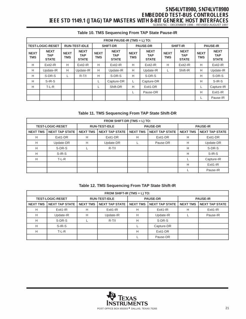
Table 10. TMS Sequencing From TAP State Pause-IR
FROM PAUSE-IR (TMS = L) TO:
TEST-LOGIC-RESET RUN-TEST-IDLE SHIFT-DR PAUSE-DR SHIFT-IR PAUSE-IR
NEXTTMS
NEXTTAP
STATE
NEXTTMS
NEXTTAP
STATE
NEXTTMS
NEXTTAP
STATE
NEXTTMS
NEXTTAP
STATE
NEXTTMS
NEXTTAP
STATE
NEXTTMS
NEXTTAP
STATE
H Exit2-IR H Exit2-IR H Exit2-IR H Exit2-IR H Exit2-IR H Exit2-IR
H Update-IR H Update-IR H Update-IR H Update-IR L Shift-IR H Update-IR
H S-DR-S L R-T/I H S-DR-S H S-DR-S H S-DR-S
H S-IR-S L Capture-DR L Capture-DR H S-IR-S
H T-L-R L Shift-DR H Exit1-DR L Capture-IR
L Pause-DR H Exit1-IR
L Pause-IR
Table 11. TMS Sequencing From TAP State Shift-DR
FROM SHIFT-DR (TMS = L) TO:
TEST-LOGIC-RESET RUN-TEST-IDLE PAUSE-DR PAUSE-IR
NEXT TMS NEXT TAP STATE NEXT TMS NEXT TAP STATE NEXT TMS NEXT TAP STATE NEXT TMS NEXT TAP STATE
H Exit1-DR H Exit1-DR H Exit1-DR H Exit1-DR
H Update-DR H Update-DR L Pause-DR H Update-DR
H S-DR-S L R-T/I H S-DR-S
H S-IR-S H S-IR-S
H T-L-R L Capture-IR
H Exit1-IR
L Pause-IR
Table 12. TMS Sequencing From TAP State Shift-IR
FROM SHIFT-IR (TMS = L) TO:
TEST-LOGIC-RESET RUN-TEST-IDLE PAUSE-DR PAUSE-IR
NEXT TMS NEXT TAP STATE NEXT TMS NEXT TAP STATE NEXT TMS NEXT TAP STATE NEXT TMS NEXT TAP STATE
H Exit1-IR H Exit1-IR H Exit1-IR H Exit1-IR
H Update-IR H Update-IR H Update-IR L Pause-IR
H S-DR-S L R-T/I H S-DR-S
H S-IR-S L Capture-DR
H T-L-R H Exit1-DR
L Pause-DR
SN54LVT8980, SN74LVT8980EMBEDDED TEST-BUS CONTROLLERSIEEE STD 1149.1 (JTAG) TAP MASTERS WITH 8-BIT GENERIC HOST INTERFACES
SCBS676C – DECEMBER 1996 – REVISED AUGUST 1997
22 POST OFFICE BOX 655303 • DALLAS, TEXAS 75265
state diagram description
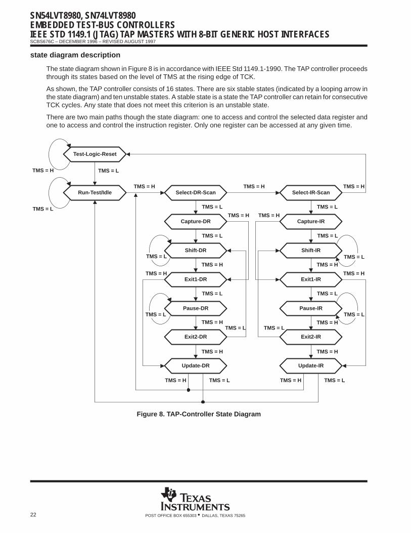
The state diagram shown in Figure 8 is in accordance with IEEE Std 1149.1-1990. The TAP controller proceedsthrough its states based on the level of TMS at the rising edge of TCK.
As shown, the TAP controller consists of 16 states. There are six stable states (indicated by a looping arrow inthe state diagram) and ten unstable states. A stable state is a state the TAP controller can retain for consecutiveTCK cycles. Any state that does not meet this criterion is an unstable state.
There are two main paths though the state diagram: one to access and control the selected data register andone to access and control the instruction register. Only one register can be accessed at any given time.
Test-Logic-Reset
Run-Test/Idle Select-DR-Scan
Capture-DR
Shift-DR
Exit1-DR
Pause-DR
Update-DR
Exit2-DR
Select-IR-Scan
Capture-IR
Shift-IR
Exit1-IR
Pause-IR
Update-IR
Exit2-IR
TMS = H TMS = L
TMS = H TMS = H
TMS = H
TMS = H
TMS = H
TMS = H
TMS = H
TMS = H
TMS = H
TMS = H
TMS = H
TMS = H
TMS = H
TMS = HTMS = HTMS = L TMS = L
TMS = L
TMS = L
TMS = L TMS = L
TMS = L
TMS = L
TMS = L
TMS = L TMS = L
TMS = L
TMS = L
TMS = L
TMS = L
Figure 8. TAP-Controller State Diagram
SN54LVT8980, SN74LVT8980EMBEDDED TEST-BUS CONTROLLERS
IEEE STD 1149.1 (JTAG) TAP MASTERS WITH 8-BIT GENERIC HOST INTERFACES
SCBS676C – DECEMBER 1996 – REVISED AUGUST 1997
23POST OFFICE BOX 655303 • DALLAS, TEXAS 75265
Test-Logic-Reset
The eTBC TAP-state generator powers up in the Test-Logic-Reset state. Alternatively, the eTBC can be forcedto this state asynchronously by assertion of its RST input or synchronously by writing the eTBC commandregister (bit 7-SWRST).
For a target device in the stable Test-Logic-Reset state, the test logic is reset and is disabled so that the normallogic function of the device is performed. The instruction register is reset to an opcode that selects the optionalIDCODE instruction, if supported, or the BYPASS instruction. Certain data registers also can be reset to theirpower-up values.
Run-Test/Idle
For a target device, Run-Test/Idle is a stable state in which the test logic can be actively running a test or canbe idle.
Select-DR-Scan, Select-lR-Scan
For a target device, no specific function is performed in the Select-DR-Scan and Select-lR-Scan states, and theTAP controller exits either of these states on the next TCK cycle. These states allow the selection of eitherdata-register scan or instruction-register scan.
Capture-DR
For a target device in the Capture-DR state, the selected data register can capture a data value as specifiedby the current instruction. Such capture operations occur on the rising edge of TCK, upon which the Capture-DRstate is exited.
Shift-DR
For a target device, upon entry to the Shift-DR state, the selected data register is placed in the scan pathbetween TDI and TDO, and on the first falling edge of TCK, TDO goes from the high-impedance state to anactive state. TDO outputs the logic level present in the least-significant bit of the selected data register. Whilein the stable Shift-DR state, data is serially shifted through the selected data register on each TCK cycle.
Exit1-DR, Exit2-DR
For a target device, the Exit1-DR and Exit2-DR states are temporary states that end a data-register scan. It ispossible to return to the Shift-DR state from either Exit1-DR or Exit2-DR without recapturing the data register.On the first falling edge of TCK after entry to Exit1-DR, TDO goes from the active state to thehigh-impedance state.
Pause-DR
For target devices, no specific function is performed in the stable Pause-DR state. The Pause-DR statesuspends and resumes data-register scan operations without loss of data.
Update-DR
For a target device, if the current instruction calls for the selected data register to be updated with current data,such update occurs on the falling edge of TCK, following entry to the Update-DR state.
Capture-IR
For a target device in the Capture-IR state, the instruction register captures its current status value. This captureoperation occurs on the rising edge of TCK, upon which the Capture-IR state is exited.
SN54LVT8980, SN74LVT8980EMBEDDED TEST-BUS CONTROLLERSIEEE STD 1149.1 (JTAG) TAP MASTERS WITH 8-BIT GENERIC HOST INTERFACES
SCBS676C – DECEMBER 1996 – REVISED AUGUST 1997
24 POST OFFICE BOX 655303 • DALLAS, TEXAS 75265
Shift-IR
For a target device, upon entry to the Shift-IR state, the instruction register is placed in the scan path betweenTDI and TDO, and on the first falling edge of TCK, TDO goes from the high-impedance state to an active state.TDO outputs the logic level present in the least-significant bit of the instruction register. While in the stableShift-IR state, instruction data is serially shifted through the instruction register on each TCK cycle.
Exit1-IR, Exit2-IR
For target devices, the Exit1-IR and Exit2-IR states are temporary states that end an instruction-register scan.It is possible to return to the Shift-IR state from either Exit1-IR or Exit2-IR without recapturing the instructionregister. On the first falling edge of TCK after entry to Exit1-IR, TDO goes from the active state to thehigh-impedance state.
Pause-IR
For target devices, no specific function is performed in the stable Pause-IR state, in which the TAP controllercan remain indefinitely. The Pause-IR state suspends and resumes instruction-register scan operations withoutloss of data.
Update-IR
For target devices, the current instruction is updated and takes effect on the falling edge of TCK, following entryto the Update-IR state.
TDO buffer
The TDO buffer is the 4 × 8-bit-parallel-to-serial FIFO that accepts scan data from the host in 8-bit-parallel formatand serializes it onto the TDO pin during scan operations. Scan data is expected to be transferred from the hostin least-significant-byte-first order to meet IEEE Std 1149.1 requirements for least-significant-bit-first scan order.Any partial byte to be written should be justified to D0. The TDO buffer is cleared upon command initiation, sono scan data should be written to the TDO buffer before writing a scan command to the command register.
The TDO-buffer status (not full/full) is maintained in the status register (bit 6, TDOS). When the TDO-bufferstatus is full, writes to the TDO buffer is held off by RDY inactive and if the write cycle is aborted prior to RDYactive, the write data is ignored.
For the convenience and efficiency of operating scans to the target for which outgoing data is not required, theeTBC supports special classes of input-only and recirculate scan commands that do not require nor operatethe TDO buffer and so the host need not perform any write access to it. While the input-only scan commandsare operating, the TDO pin outputs a fixed high level. While the recirculate scan commands are operating, theTDO pin recirculates to the target the data that is received at TDI.
While the eTBC is in discrete-control mode, the TDO buffer is not used; instead, the state of the TDO pin isdetermined by the contents of the discrete-control register. Thus, TMS/TDO sequences that cannot beautomatically generated still can be applied through the eTBC to targets that require such (e.g., near-compliantdevices).
For eTBC verification/debugging, the TDO-buffer output can be selected for loopback into the TDI buffer. Whenthis TDO-loopback mode is selected, although a host-requested command executes in the eTBC, the targetis not affected, as both TMS and TDI are fixed at a high level.
Upon eTBC reset (power up, hardware initiated, or software initiated), the TDO buffer is cleared and assumesits not-full state.

SN54LVT8980, SN74LVT8980EMBEDDED TEST-BUS CONTROLLERS
IEEE STD 1149.1 (JTAG) TAP MASTERS WITH 8-BIT GENERIC HOST INTERFACES
SCBS676C – DECEMBER 1996 – REVISED AUGUST 1997
25POST OFFICE BOX 655303 • DALLAS, TEXAS 75265
TDI buffer
The TDI buffer is the serial-to-4 × 8-bit-parallel FIFO that serially receives data at the TDI pin and makes itavailable in 8-bit-parallel format for reading by the host. Scan data is expected to be transferred from theIEEE Std 1149.1 targets in least-significant-bit-first order and is made available for host read inleast-significant-byte-first order. The last data available for host read during a scan command may be a partialbyte, in which case it is justified to D0.
The TDI-buffer status (empty/not empty) is maintained in the status register (bit 7, TDIS). When the TDI-bufferstatus is empty, reads to the TDI buffer is held off by RDY inactive and, if the read cycle is aborted prior to RDYactive, the read data is invalid.
The TDI buffer is able to automatically accommodate retiming (pipeline) delays to the target. While operatinga scan command, TDI sampling is delayed by a number of TCK cycles, equal to a value given in theconfigurationB register (bits 3–0, RDLY), following the generation of Shift-DR or Shift-IR state, as appropriate.
For the convenience and efficiency of operating scans to the target for which incoming data is not required, theeTBC supports a special class of output-only scan commands that neither require nor operate the TDI buffer.While the output-only scan commands are operating, the data received at TDI is ignored and the host need notperform any read access to the TDI buffer.
While the eTBC is in discrete-control mode, the TDI buffer is not used; instead, the state of the TDO pin isobserved in the discrete-control register. Thus, TMS/TDO sequences that cannot be automatically generatedcan still be applied through the eTBC to targets that require such (e.g., near-compliant devices).
For eTBC verification/debugging, the input to the TDI buffer can be selected for loopback from either TDO bufferor TAP-state (TMS) generator. When either of these loopback modes is selected, although a host-requestedcommand executes in the eTBC, the target is not affected, as both TMS and TDI are fixed at a high level.
Upon eTBC reset (power up, hardware initiated, or software initiated), the TDI buffer is cleared and assumesits empty state.
discrete control
The discrete-control block provides the multiplexing and control logic required to support the eTBC’sdiscrete-control mode in addition to its automatic modes. While the eTBC is in discrete-control mode, the TAPsignals are fully controllable/accessible to the host via reads/writes to the discrete-control register. Nocommands can be initiated/operated while the eTBC is in the discrete-control mode.
Upon eTBC reset (power up, hardware initiated, or software initiated), the discrete-control mode is inactive.
reset
The eTBC provides three mechanisms for comprehensive and equivalent reset – power-up reset,hardware-initiated reset (RST), and software-initiated reset (SWRST, bit 7 of command register) to thefollowing effect:
All eTBC registers are reset to default values as given in Table 1.
The command/control logic is fully reset.
The counter is cleared/unloaded. The TDO buffer and TDI buffer are cleared/emptied.
The TAP-state generator is reset to the Test-Logic-Reset TAP state.
TDO, TMS, and TRST output high levels; TCK outputs CLKIN/16.
As a consequence, the IEEE Std 1149.1 targets can be expected to be driven synchronously to theTest-Logic-Reset state no later than the fifth rising edge of TCK (72 CLKIN cycles).
SN54LVT8980, SN74LVT8980EMBEDDED TEST-BUS CONTROLLERSIEEE STD 1149.1 (JTAG) TAP MASTERS WITH 8-BIT GENERIC HOST INTERFACES
SCBS676C – DECEMBER 1996 – REVISED AUGUST 1997
26 POST OFFICE BOX 655303 • DALLAS, TEXAS 75265
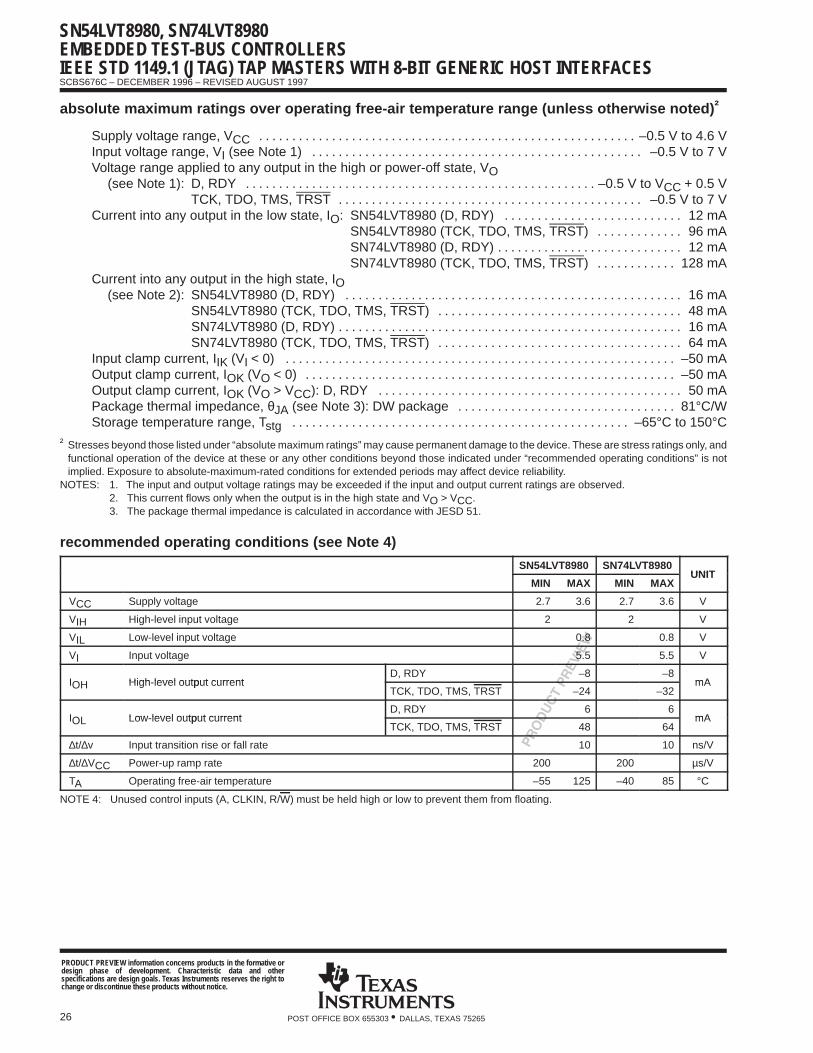
absolute maximum ratings over operating free-air temperature range (unless otherwise noted) †
Supply voltage range, VCC –0.5 V to 4.6 V. . . . . . . . . . . . . . . . . . . . . . . . . . . . . . . . . . . . . . . . . . . . . . . . . . . . . . . . . Input voltage range, VI (see Note 1) –0.5 V to 7 V. . . . . . . . . . . . . . . . . . . . . . . . . . . . . . . . . . . . . . . . . . . . . . . . . . Voltage range applied to any output in the high or power-off state, VO
(see Note 1): D, RDY –0.5 V to VCC + 0.5 V. . . . . . . . . . . . . . . . . . . . . . . . . . . . . . . . . . . . . . . . . . . . . . . . . . . . . TCK, TDO, TMS, TRST –0.5 V to 7 V. . . . . . . . . . . . . . . . . . . . . . . . . . . . . . . . . . . . . . . . . . . . . .
Current into any output in the low state, IO: SN54LVT8980 (D, RDY) 12 mA. . . . . . . . . . . . . . . . . . . . . . . . . . . SN54LVT8980 (TCK, TDO, TMS, TRST) 96 mA. . . . . . . . . . . . . SN74LVT8980 (D, RDY) 12 mA. . . . . . . . . . . . . . . . . . . . . . . . . . . . SN74LVT8980 (TCK, TDO, TMS, TRST) 128 mA. . . . . . . . . . . .
Current into any output in the high state, IO(see Note 2): SN54LVT8980 (D, RDY) 16 mA. . . . . . . . . . . . . . . . . . . . . . . . . . . . . . . . . . . . . . . . . . . . . . . . . . .
SN54LVT8980 (TCK, TDO, TMS, TRST) 48 mA. . . . . . . . . . . . . . . . . . . . . . . . . . . . . . . . . . . . . SN74LVT8980 (D, RDY) 16 mA. . . . . . . . . . . . . . . . . . . . . . . . . . . . . . . . . . . . . . . . . . . . . . . . . . . . SN74LVT8980 (TCK, TDO, TMS, TRST) 64 mA. . . . . . . . . . . . . . . . . . . . . . . . . . . . . . . . . . . . .
Input clamp current, IIK (VI < 0) –50 mA. . . . . . . . . . . . . . . . . . . . . . . . . . . . . . . . . . . . . . . . . . . . . . . . . . . . . . . . . . . Output clamp current, IOK (VO < 0) –50 mA. . . . . . . . . . . . . . . . . . . . . . . . . . . . . . . . . . . . . . . . . . . . . . . . . . . . . . . . Output clamp current, IOK (VO > VCC): D, RDY 50 mA. . . . . . . . . . . . . . . . . . . . . . . . . . . . . . . . . . . . . . . . . . . . . . Package thermal impedance, θJA (see Note 3): DW package 81°C/W. . . . . . . . . . . . . . . . . . . . . . . . . . . . . . . . . Storage temperature range, Tstg –65°C to 150°C. . . . . . . . . . . . . . . . . . . . . . . . . . . . . . . . . . . . . . . . . . . . . . . . . . .
† Stresses beyond those listed under “absolute maximum ratings” may cause permanent damage to the device. These are stress ratings only, andfunctional operation of the device at these or any other conditions beyond those indicated under “recommended operating conditions” is notimplied. Exposure to absolute-maximum-rated conditions for extended periods may affect device reliability.
NOTES: 1. The input and output voltage ratings may be exceeded if the input and output current ratings are observed.2. This current flows only when the output is in the high state and VO > VCC.3. The package thermal impedance is calculated in accordance with JESD 51.
recommended operating conditions (see Note 4)
SN54LVT8980 SN74LVT8980UNIT
MIN MAX MIN MAXUNIT
VCC Supply voltage 2.7 3.6 2.7 3.6 V
VIH High-level input voltage 2 2 V
VIL Low-level input voltage 0.8 0.8 V
VI Input voltage 5.5 5.5 V
IOH High level output currentD, RDY –8 –8
mAIOH High-level output currentTCK, TDO, TMS, TRST –24 –32
mA
IOL Low level output currentD, RDY 6 6
mAIOL Low-level output currentTCK, TDO, TMS, TRST 48 64
mA
∆t/∆v Input transition rise or fall rate 10 10 ns/V
∆t/∆VCC Power-up ramp rate 200 200 µs/V
TA Operating free-air temperature –55 125 –40 85 °C
NOTE 4: Unused control inputs (A, CLKIN, R/W) must be held high or low to prevent them from floating.
PRODUCT PREVIEW information concerns products in the formative ordesign phase of development. Characteristic data and otherspecifications are design goals. Texas Instruments reserves the right tochange or discontinue these products without notice.
SN54LVT8980, SN74LVT8980EMBEDDED TEST-BUS CONTROLLERS
IEEE STD 1149.1 (JTAG) TAP MASTERS WITH 8-BIT GENERIC HOST INTERFACES
SCBS676C – DECEMBER 1996 – REVISED AUGUST 1997
27POST OFFICE BOX 655303 • DALLAS, TEXAS 75265
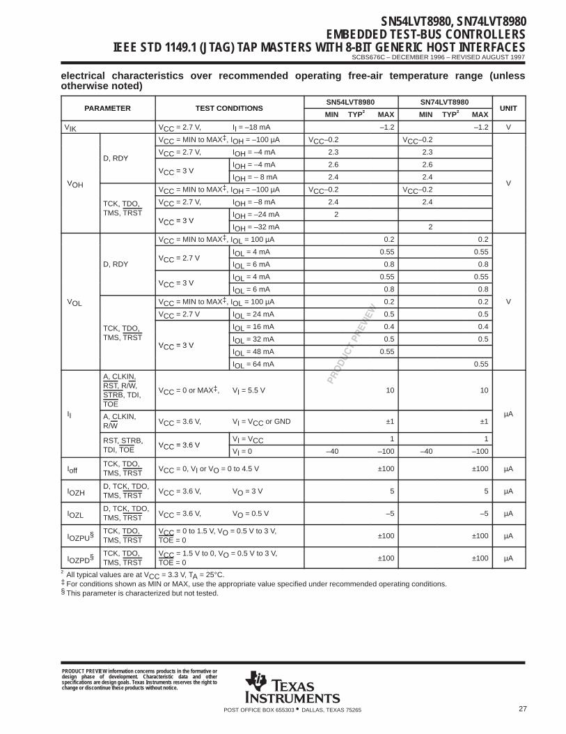
electrical characteristics over recommended operating free-air temperature range (unlessotherwise noted)
PARAMETER TEST CONDITIONSSN54LVT8980 SN74LVT8980
UNITPARAMETER TEST CONDITIONSMIN TYP† MAX MIN TYP† MAX
UNIT
VIK VCC = 2.7 V, II = –18 mA –1.2 –1.2 V
VCC = MIN to MAX‡, IOH = –100 µA VCC–0.2 VCC–0.2
D RDYVCC = 2.7 V, IOH = –4 mA 2.3 2.3
D, RDY
VCC = 3 VIOH = –4 mA 2.6 2.6
VOH
VCC = 3 VIOH = – 8 mA 2.4 2.4
VVOHVCC = MIN to MAX‡, IOH = –100 µA VCC–0.2 VCC–0.2
V
TCK, TDO, VCC = 2.7 V, IOH = –8 mA 2.4 2.4, ,TMS, TRST
VCC = 3 VIOH = –24 mA 2
VCC = 3 VIOH = –32 mA 2
VCC = MIN to MAX‡, IOL = 100 µA 0.2 0.2
VCC = 2 7 VIOL = 4 mA 0.55 0.55
D, RDYVCC = 2.7 V
IOL = 6 mA 0.8 0.8
VCC = 3 VIOL = 4 mA 0.55 0.55
VCC = 3 VIOL = 6 mA 0.8 0.8
VOL VCC = MIN to MAX‡, IOL = 100 µA 0.2 0.2 V
VCC = 2.7 V IOL = 24 mA 0.5 0.5
TCK, TDO, IOL = 16 mA 0.4 0.4, ,TMS, TRST
VCC = 3 VIOL = 32 mA 0.5 0.5
VCC = 3 VIOL = 48 mA 0.55
IOL = 64 mA 0.55
A, CLKIN,RST, R/W,STRB, TDI,TOE
VCC = 0 or MAX‡, VI = 5.5 V 10 10
II A, CLKIN,R/W
VCC = 3.6 V, VI = VCC or GND ±1 ±1µA
RST, STRB,VCC = 3 6 V
VI = VCC 1 1, ,TDI, TOE
VCC = 3.6 VVI = 0 –40 –100 –40 –100
IoffTCK, TDO,TMS, TRST
VCC = 0, VI or VO = 0 to 4.5 V ±100 ±100 µA
IOZHD, TCK, TDO,TMS, TRST
VCC = 3.6 V, VO = 3 V 5 5 µA
IOZLD, TCK, TDO,TMS, TRST
VCC = 3.6 V, VO = 0.5 V –5 –5 µA
IOZPU§ TCK, TDO,TMS, TRST
VCC = 0 to 1.5 V, VO = 0.5 V to 3 V,TOE = 0
±100 ±100 µA
IOZPD§ TCK, TDO,TMS, TRST
VCC = 1.5 V to 0, VO = 0.5 V to 3 V,TOE = 0
±100 ±100 µA
† All typical values are at VCC = 3.3 V, TA = 25°C.‡ For conditions shown as MIN or MAX, use the appropriate value specified under recommended operating conditions.§ This parameter is characterized but not tested.
PRODUCT PREVIEW information concerns products in the formative ordesign phase of development. Characteristic data and otherspecifications are design goals. Texas Instruments reserves the right tochange or discontinue these products without notice.

SN54LVT8980, SN74LVT8980EMBEDDED TEST-BUS CONTROLLERSIEEE STD 1149.1 (JTAG) TAP MASTERS WITH 8-BIT GENERIC HOST INTERFACES
SCBS676C – DECEMBER 1996 – REVISED AUGUST 1997
28 POST OFFICE BOX 655303 • DALLAS, TEXAS 75265
electrical characteristics over recommended operating free-air temperature range (unlessotherwise noted) (continued)
PARAMETER TEST CONDITIONSSN54LVT8980 SN74LVT8980
UNITPARAMETER TEST CONDITIONSMIN TYP† MAX MIN TYP† MAX
UNIT
Outputs high 0.5 0.5
ICCOutputs low
VCC = 3 6 V IO = 0 VI = VCC or GND7 7
mAICCOutputsdisabled
VCC = 3.6 V, IO = 0, VI = VCC or GND
0.5 0.5
mA
∆ICC¶VCC = 3 V to 3.6 V,One input at VCC – 0.6 V,Other inputs at VCC or GND
0.2 0.2 mA
Ci VI = 3 V or 0 4 4 pF
Cio VO = 3 V or 0 5 5 pF
Co VO = 3 V or 0 7 7 pF
† All typical values are at VCC = 3.3 V, TA = 25°C.¶ This is the increase in supply current for each input that is at the specified TTL voltage level rather than VCC or GND.
timing requirements over recommended operating free-air temperature range (unless otherwisenoted) (see Figures 9 and 10)
SN54LVT8980 SN74LVT8980
VCC = 3.3 V± 0.3 V VCC = 2.7 V
VCC = 3.3 ± 0.3 V VCC = 2.7 V UNIT
MIN MAX MIN MAX MIN MAX MIN MAX
TCK = CLKIN(CDIV = 0)
0 20 0 16 0 20 0 16
fclock Clock frequency, CLKINTCK = CLKIN/2(CDIV = 1)
0 40 0 32 0 40 0 32 MHz
TCK ≤ CLKIN/4(CDIV ≥ 2)
0 70 0 64 0 70 0 64
TCK = CLKIN(CDIV = 0)
25 31 25 31
tPulse
CLKINhigh or low
TCK = CLKIN/2(CDIV = 1)
12.5 15.6 12.5 15.6
twPulseduration TCK ≤ CLKIN/4
(CDIV ≥ 2)7.1 7.8 7.1 7.8
ns
RST low 10 10 10 10
STRB low 8 8 8 8
A before STRB↓Read or write(R/W high or low)
10 10 10 10
tsu Setup time D before STRB↑ Write (R/W low) 5 5 5 5 nssuR/W before STRB↓ 5 5 5 5
TDI before CLKIN↑ 5 5 5 5
A after STRB↑Read or write(R/W high or low)
5 5 5 5
th Hold time D after STRB↑ Write (R/W low) 15 15 15 15 nshR/W after STRB↑ 6 6 6 6
TDI after CLKIN↑ 10 10 10 10
PRODUCT PREVIEW information concerns products in the formative ordesign phase of development. Characteristic data and otherspecifications are design goals. Texas Instruments reserves the right tochange or discontinue these products without notice.
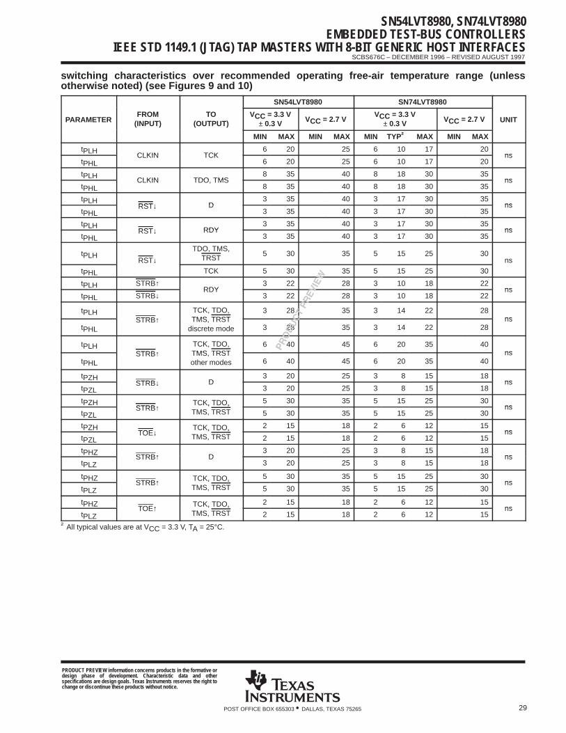
SN54LVT8980, SN74LVT8980EMBEDDED TEST-BUS CONTROLLERS
IEEE STD 1149.1 (JTAG) TAP MASTERS WITH 8-BIT GENERIC HOST INTERFACES
SCBS676C – DECEMBER 1996 – REVISED AUGUST 1997
29POST OFFICE BOX 655303 • DALLAS, TEXAS 75265
switching characteristics over recommended operating free-air temperature range (unlessotherwise noted) (see Figures 9 and 10)
SN54LVT8980 SN74LVT8980
PARAMETERFROM
(INPUT)TO
(OUTPUT)VCC = 3.3 V
± 0.3 V VCC = 2.7 VVCC = 3.3 V
± 0.3 V VCC = 2.7 V UNIT
MIN MAX MIN MAX MIN TYP† MAX MIN MAX
tPLHCLKIN TCK
6 20 25 6 10 17 20ns
tPHLCLKIN TCK
6 20 25 6 10 17 20ns
tPLHCLKIN TDO TMS
8 35 40 8 18 30 35ns
tPHLCLKIN TDO, TMS
8 35 40 8 18 30 35ns
tPLHRST↓ D
3 35 40 3 17 30 35ns
tPHLRST↓ D
3 35 40 3 17 30 35ns
tPLHRST↓ RDY
3 35 40 3 17 30 35ns
tPHLRST↓ RDY
3 35 40 3 17 30 35ns
tPLHRST↓
TDO, TMS,TRST
5 30 35 5 15 25 30ns
tPHL TCK 5 30 35 5 15 25 30
tPLH STRB↑RDY
3 22 28 3 10 18 22ns
tPHL STRB↓RDY
3 22 28 3 10 18 22ns
tPLHSTRB↑
TCK, TDO,TMS TRST
3 28 35 3 14 22 28ns
tPHLSTRB↑ TMS, TRST
discrete mode 3 28 35 3 14 22 28ns
tPLHSTRB↑
TCK, TDO,TMS TRST
6 40 45 6 20 35 40ns
tPHLSTRB↑ TMS, TRST
other modes 6 40 45 6 20 35 40ns
tPZHSTRB↓ D
3 20 25 3 8 15 18ns
tPZLSTRB↓ D
3 20 25 3 8 15 18ns
tPZHSTRB↑
TCK, TDO, 5 30 35 5 15 25 30ns
tPZLSTRB↑
, ,TMS, TRST 5 30 35 5 15 25 30
ns
tPZHTOE↓
TCK, TDO, 2 15 18 2 6 12 15ns
tPZLTOE↓
, ,TMS, TRST 2 15 18 2 6 12 15
ns
tPHZSTRB↑ D
3 20 25 3 8 15 18ns
tPLZSTRB↑ D
3 20 25 3 8 15 18ns
tPHZSTRB↑ TCK, TDO, 5 30 35 5 15 25 30
nstPLZ
STRB↑ , ,TMS, TRST 5 30 35 5 15 25 30
ns
tPHZTOE↑ TCK, TDO, 2 15 18 2 6 12 15
nstPLZ
TOE↑ , ,TMS, TRST 2 15 18 2 6 12 15
ns
† All typical values are at VCC = 3.3 V, TA = 25°C.
PRODUCT PREVIEW information concerns products in the formative ordesign phase of development. Characteristic data and otherspecifications are design goals. Texas Instruments reserves the right tochange or discontinue these products without notice.

SN54LVT8980, SN74LVT8980EMBEDDED TEST-BUS CONTROLLERSIEEE STD 1149.1 (JTAG) TAP MASTERS WITH 8-BIT GENERIC HOST INTERFACES
SCBS676C – DECEMBER 1996 – REVISED AUGUST 1997
30 POST OFFICE BOX 655303 • DALLAS, TEXAS 75265
PARAMETER MEASUREMENT INFORMATION
thtsu
From OutputUnder Test
CL = 50 pF(see Note A)
LOAD CIRCUIT
S1
4 V
500 Ω
500 Ω
Data Input
Timing Input2.7 V
0 V
2.7 V
0 V
2.7 V
0 V
tw
Input
VOLTAGE WAVEFORMSSETUP AND HOLD TIMES
VOLTAGE WAVEFORMSPROPAGATION DELAY TIMES
INVERTING AND NONINVERTING OUTPUTS
VOLTAGE WAVEFORMSPULSE DURATION
tPLH
tPHL
tPHL
tPLH
VOH
VOH
VOL
VOL
2.7 V
0 V
Input OutputControl
OutputWaveform 1
S1 at 6 V(see Note B)
OutputWaveform 2
S1 at GND(see Note B)
VOL
VOH
tPZL
tPZH
tPLZ
tPHZ
2 V
0 V
VOL + 0.3 V
VOH – 0.3 V
≈ 0 V
2.7 V
VOLTAGE WAVEFORMSENABLE AND DISABLE TIMES
LOW- AND HIGH-LEVEL ENABLING
Output
Output
tPLH/tPHLtPLZ/tPZLtPHZ/tPZH
Open4 V
GND
TEST S1
NOTES: A. CL includes probe and jig capacitance.B. Waveform 1 is for an output with internal conditions such that the output is low except when disabled by the output control.
Waveform 2 is for an output with internal conditions such that the output is high except when disabled by the output control.C. All input pulses are supplied by generators having the following characteristics: PRR ≤ 10 MHz, ZO = 50 Ω, tr ≤ 2.5 ns, tf ≤ 2.5 ns.D. The outputs are measured one at a time with one transition per measurement.
Open
1.5 V 1.5 V
1.5 V 1.5 V
1.5 V 1.5 V
1.5 V 1.5 V
1.5 V
1.5 V 1.5 V
1.5 V 1.5 V
1.5 V
1.5 V
Figure 9. Load Circuit and Voltage Waveforms (D and RDY Outputs)
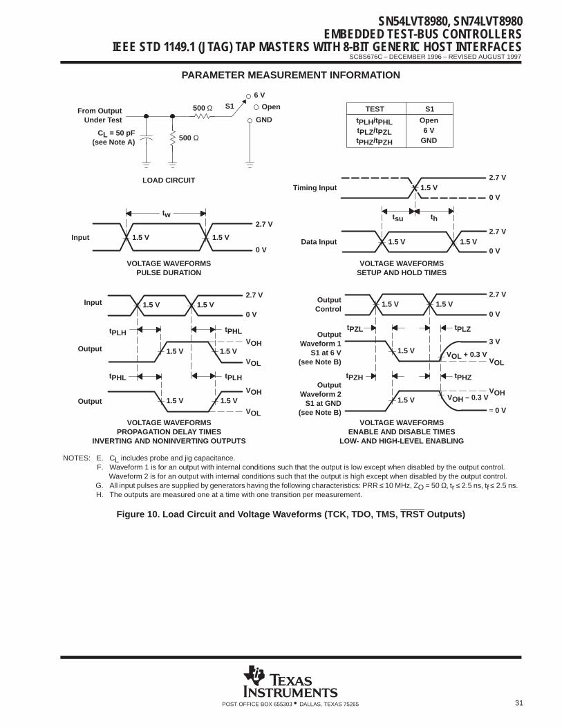
SN54LVT8980, SN74LVT8980EMBEDDED TEST-BUS CONTROLLERS
IEEE STD 1149.1 (JTAG) TAP MASTERS WITH 8-BIT GENERIC HOST INTERFACES
SCBS676C – DECEMBER 1996 – REVISED AUGUST 1997
31POST OFFICE BOX 655303 • DALLAS, TEXAS 75265
PARAMETER MEASUREMENT INFORMATION
thtsu
From OutputUnder Test
CL = 50 pF(see Note A)
LOAD CIRCUIT
S1
6 V
GND
500 Ω
500 Ω
Data Input
Timing Input2.7 V
0 V
2.7 V
0 V
2.7 V
0 V
tw
Input
VOLTAGE WAVEFORMSSETUP AND HOLD TIMES
VOLTAGE WAVEFORMSPROPAGATION DELAY TIMES
INVERTING AND NONINVERTING OUTPUTS
VOLTAGE WAVEFORMSPULSE DURATION
tPLH
tPHL
tPHL
tPLH
VOH
VOH
VOL
VOL
2.7 V
0 V
Input OutputControl
OutputWaveform 1
S1 at 6 V(see Note B)
OutputWaveform 2
S1 at GND(see Note B)
VOL
VOH
tPZL
tPZH
tPLZ
tPHZ
3 V
0 V
VOL + 0.3 V
VOH – 0.3 V
≈ 0 V
2.7 V
VOLTAGE WAVEFORMSENABLE AND DISABLE TIMES
LOW- AND HIGH-LEVEL ENABLING
Output
Output
tPLH/tPHLtPLZ/tPZLtPHZ/tPZH
Open6 V
GND
TEST S1
NOTES: E. CL includes probe and jig capacitance.F. Waveform 1 is for an output with internal conditions such that the output is low except when disabled by the output control.
Waveform 2 is for an output with internal conditions such that the output is high except when disabled by the output control.G. All input pulses are supplied by generators having the following characteristics: PRR ≤ 10 MHz, ZO = 50 Ω, tr ≤ 2.5 ns, tf ≤ 2.5 ns.H. The outputs are measured one at a time with one transition per measurement.
Open
1.5 V 1.5 V
1.5 V 1.5 V
1.5 V 1.5 V
1.5 V 1.5 V
1.5 V
1.5 V 1.5 V
1.5 V 1.5 V
1.5 V
1.5 V
Figure 10. Load Circuit and Voltage Waveforms (TCK, TDO, TMS, TRST Outputs)
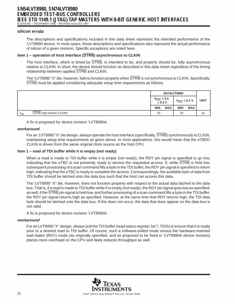
SN54LVT8980, SN74LVT8980EMBEDDED TEST-BUS CONTROLLERSIEEE STD 1149.1 (JTAG) TAP MASTERS WITH 8-BIT GENERIC HOST INTERFACES
SCBS676C – DECEMBER 1996 – REVISED AUGUST 1997
32 POST OFFICE BOX 655303 • DALLAS, TEXAS 75265
silicon errata
The descriptions and specifications included in this data sheet represent the intended performance of the’LVT8990 device. In most cases, these descriptions and specifications also represent the actual performanceof silicon of a given revision. Specific exceptions are noted here.
item 1 – operation of host interface (STRB ) asynchronous to CLKIN
The host interface, which is timed by STRB, is intended to be, and properly should be, fully asynchronousrelative to CLKIN. In short, the device should function as described in this data sheet regardless of the timingrelationship between applied STRB and CLKIN.
The ’LVT8990 “X” die, however, fails to function properly when STRB is not synchronous to CLKIN. Specifically,STRB must be applied considering adequate setup time requirements as follows:
SN74LVT8980
VCC = 3.3 ± 0.3 V VCC = 2.7 V UNIT
MIN MAX MIN MAX
tsu STRB high before CLKIN↑ 25 25 ns
A fix is proposed for device revision ’LVT8980A.
workaround
For an ’LVT8980 “X” die design, always operate the host interface (specifically, STRB) synchronously to CLKIN,maintaining setup time requirements as given above. In most applications, this would mean that the eTBDCCLKIN is driven from the same original clock source as the host CPU.
item 1 – read of TDI buffer while it is empty (not ready)
When a read is made to TDI buffer while it is empty (not ready), the RDY pin signal is specified to go low,indicating that the eTBC is not presently ready to service the requested access. If, while STRB is held low,subsequent processing of a scan command fills a byte in the TDI buffer, the RDY pin signal is specified to returnhigh, indicating that the eTBC is ready to complete the access. Correspondingly, the available byte of data fromTDI buffer should be latched onto the data bus such that the host can access this data.
The ’LVT8990 “X” die, however, does not function properly with respect to the actual data latched to the databus. That is, if a read is made to TDI buffer while it is empty (not ready), the RDY pin signal goes low as specified;as well, if the STRB pin signal is held low, and further processing of a scan command fills a byte in the TDI buffer,the RDY pin signal returns high as specified. However, at the same time that RDY returns high, the TDI databyte should be latched onto the data bus. If this does not occur, the data that does appear on the data bus isnot valid.
A fix is proposed for device revision ’LVT8980A.
workaround
For an LVT8990 “X” design, always poll the TDI buffer (read status register, bit 7, TDIS) to ensure that it is readyprior to a desired read to TDI buffer. Of course, such a software-polled mode versus the hardware-insertedwait-states (RDY) mode (as originally specified, and as proposed to be fixed in ’LVT8980A device revision)places more overhead on the CPU and likely reduces throughput as well.
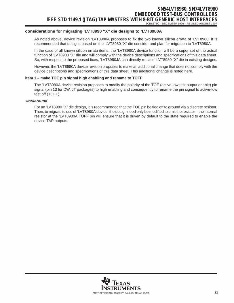
SN54LVT8980, SN74LVT8980EMBEDDED TEST-BUS CONTROLLERS
IEEE STD 1149.1 (JTAG) TAP MASTERS WITH 8-BIT GENERIC HOST INTERFACES
SCBS676C – DECEMBER 1996 – REVISED AUGUST 1997
33POST OFFICE BOX 655303 • DALLAS, TEXAS 75265
considerations for migrating ’LVT8990 “X” die designs to ’LVT8980A
As noted above, device revision ’LVT8980A proposes to fix the two known silicon errata of ’LVT8980. It isrecommended that designs based on the ’LVT8980 “X” die consider and plan for migration to ’LVT8980A.
In the case of all known silicon errata items, the ’LVT8980A device function will be a super set of the actualfunction of ’LVT8980 “X” die and will comply with the device descriptions and specifications of this data sheet.So, with respect to the proposed fixes, ’LVT8980JA can directly replace ’LVT8980 “X” die in existing designs.
However, the ’LVT8980A device revision proposes to make an additional change that does not comply with thedevice descriptions and specifications of this data sheet. This additional change is noted here.
item 1 – make TOE pin signal high enabling and rename to TOFF
The ’LVT8980A device revision proposes to modify the polarity of the TOE (active-low test output enable) pinsignal (pin 13 for DW, JT packages) to high enabling and consequently to rename the pin signal to active-lowtest off (TOFF).
workaround
For an ’LVT8980 “X” die design, it is recommended that the TOE pin be tied off to ground via a discrete resistor.Then, to migrate to use of ’LVT8980A device, the design need only be modified to omit the resistor – the internalresistor at the ’LVT8980A TOFF pin will ensure that it is driven by default to the state required to enable thedevice TAP outputs.
IMPORTANT NOTICE
Texas Instruments and its subsidiaries (TI) reserve the right to make changes to their products or to discontinueany product or service without notice, and advise customers to obtain the latest version of relevant informationto verify, before placing orders, that information being relied on is current and complete. All products are soldsubject to the terms and conditions of sale supplied at the time of order acknowledgement, including thosepertaining to warranty, patent infringement, and limitation of liability.
TI warrants performance of its semiconductor products to the specifications applicable at the time of sale inaccordance with TI’s standard warranty. Testing and other quality control techniques are utilized to the extentTI deems necessary to support this warranty. Specific testing of all parameters of each device is not necessarilyperformed, except those mandated by government requirements.
CERTAIN APPLICATIONS USING SEMICONDUCTOR PRODUCTS MAY INVOLVE POTENTIAL RISKS OFDEATH, PERSONAL INJURY, OR SEVERE PROPERTY OR ENVIRONMENTAL DAMAGE (“CRITICALAPPLICATIONS”). TI SEMICONDUCTOR PRODUCTS ARE NOT DESIGNED, AUTHORIZED, ORWARRANTED TO BE SUITABLE FOR USE IN LIFE-SUPPORT DEVICES OR SYSTEMS OR OTHERCRITICAL APPLICATIONS. INCLUSION OF TI PRODUCTS IN SUCH APPLICATIONS IS UNDERSTOOD TOBE FULLY AT THE CUSTOMER’S RISK.
In order to minimize risks associated with the customer’s applications, adequate design and operatingsafeguards must be provided by the customer to minimize inherent or procedural hazards.
TI assumes no liability for applications assistance or customer product design. TI does not warrant or representthat any license, either express or implied, is granted under any patent right, copyright, mask work right, or otherintellectual property right of TI covering or relating to any combination, machine, or process in which suchsemiconductor products or services might be or are used. TI’s publication of information regarding any thirdparty’s products or services does not constitute TI’s approval, warranty or endorsement thereof.
Copyright 1998, Texas Instruments Incorporated