elysium journal of engineering -...
TRANSCRIPT


ELYSIUM JOURNAL OF ENGINEERING
RESEARCH AND MANAGEMENT
DECEMBER 2015 | VOLUME 02 | ISSUE 06
ELYSIUM JOURNAL OF ENGINEERING RESEARCH AND MANAGEMENT
VOL.2 DECEMBER 2015 NO.6
S.NO TABLE OF CONTENTS Page No
1. An Efficient High Speed VCS Updation Based Mesh Topology NoC Router
Architecture Design Yedla Harika
1, T.Vishnumurthy
2 1
2. An Efficient Activity Tracking and Recognition Using the Neural Network
Classifier
G.Karthic1, B.Lalitha
2 5
3. Design of Low Power 32-Bit CSKA for High Speed Applications C.Yamini
1, M.Krishnamurthy
2 11
4. High Speed and Low Power CMOS Technology Based Ram-Cam Memory Design
K.Vidhya kamu1 and Mr.P.Karthikeyan
2 14
5. Design and Implementation of 32 Bit ALU Using Look Ahead Clock Gating Based
On FPGA
V. Prasanth1, M. Sri Manikyamba
2 17

P-ISSN: 2347-4408
E-ISSN: 2347-4734
1| Page December 2015 Volume – 2, Issue - 6
AN EFFICIENT HIGH SPEED VCS UPDATION BASED MESH TOPOLOGY NOC
ROUTER ARCHITECTURE DESIGN
Yedla Harika1, T.Vishnumurthy
2
1Department of Electronics and Communication Engineering, Pragati Engineering College, affiliated to JNTU Kakinada,
Surampalem, Andhra pradesh-533437. Email id: [email protected] 2Assistant Professor, Department of Electronics and Communication, Pragati Engineering College, affiliated to JNTU
Kakinada, Surampalem, Andhra pradesh-533437. Email id: tamminenivishnu @gmail.com
Abstract- Network-on-Chip (NoC) architectures signify a capable
design paradigm to cope with raising communication requirements
in digital systems. It emerged as a vital factor that defines the
presentation and power consumption of many core systems. VLSI
technology is to modify NOC internal router arrangements, shortest
path allocation process and neighbor router estimation control.
Existing system is to design a mesh topology based network on chip
architecture. This architecture is to implement the packet and circuit
switching for path allocation process. Existing system is to improve
the path allocation time and to effectively transmit the source to
destination processing time level. Existing time is to raise the circuit
complexity level and it consume more time for circuit analysis
process. Proposed system is to design a mesh topology based router
architecture design and to develop the path allocation process using
hybrid scheme. This scheme is to consist of VCS, CS and PS
technique for path allocation work. Proposed system is used to
implement the single router data transfer process in slave and master
router condition and to upgrade the path selection complexity level.
This technique is to reduce data transmission time between source
and destination. Proposed system is to raise the system speed level
(clock frequency). Proposed system is to reduce the delay time level
and to reduce the latency time.
Index terms- NoC, latency, VCS technique.
1. INTRODUCTION
With the rapid growth of advanced nanometer IC
technology, continuously shrinking transistor dimensions allow
designers to integrate and enhancing the IP cores or no of
processors into a single chip. Traditional bus-based
communication is no longer suitable due to its poor scalability.
Instead, network-on-chip (NoC) has derived as a scalable and
promising solution to global communications within large
multicore systems. The pipeline stages of a baseline PS router
contains the switch allocation (SA) stage, the buffer write (BW)
stage, the switch traversal (ST) stage, the route computation
(RC) stage, and the virtual channel allocation (VA) stage. The
convoluted router pipeline points to a high latency ratio.
Although look ahead routing and aggressive speculation
shorten the critical path through the router stages. In a mesh-
connected NOC, the PS router still conquers a high ratio of
communication latency when related with the one cycle
connection delay. The convoluted router pipeline leads to a
high power ratio and lacks the flexibility in circuit switching. If
numerous communications participate for a common physical
channel, circuits will be set up in turn.
In NOC the lengthy setup time will reduce the overall
performance. The hybrid system is merging with the circuit and
packet switching is proposed to solve the difficulties in
switching. It not only delivers the communications in high
flexibility, it also creating the CS connections between
communication pairs to improve the latency. In traffic with
light congestion, maximum communications is solved through
the circuit switching. But, traffic with high congestion, a very
small ratio of CS links to communications may be gained to
confines the power and latency for NOCs.
In summary, main influences of this paper are scheduled as
follows.
1) Virtual circuit switching is first introduced in this paper, and
the modified router architecture and its corresponding
switching mechanism are presented to support the
recommended hybrid system.
2) Based on virtual circuit, this paper proposes a path allocation
procedure to enhance the power consumption and
communication latency.
3) The efficiency of the recommended hybrid scheme is
established by associating with the baseline packed switched
NoC and VIP design using a set of synthetic and real traffic
workloads.
2. ARCHITECTURE
In the recommended hybrid system the basic principle is
that VCs are exploits in virtual circuit to form a no of VCS
networks. The multiple VCS networks share a common
channel.
In this hybrid system, VCS connections cooperate with CS and
PS networks to transmit packets in which physical channels are
shared by additional communication, respectively.(x,y) denotes
the physical channel from node to node y. Connections after
using the conventional hybrid scheme. A CS connection is
designed by record the each router which input port should be
attached with the output port. It is composed of physical
channels and routers. However, routers on a PS connection are
formed through the (VA, SA, RC, and BW) stages when flits
require passing through. A multiple PS and 1 CS connections
are shared by physical channel. In the CS connections flits
attain at crossbar switches, routers are instantly configured so
that the CS flits can bypass directly to the ST stage. When there
is no CS flit, the corresponding ports of crossbar switches are
released to PS connections.

P-ISSN: 2347-4408
E-ISSN: 2347-4734
2| Page December 2015 Volume – 2, Issue - 6
3. MODULES OF ARCHITECTURE
Figure 1. Block diagram
The master memory block is used to recover the destination
data for the router architecture and to analysis the destination
selection level also .The master process work is used to select
the output data to the next node selection data. The single router
architecture is to port the router architecture level and to check
the master selection processing level. The single router design
is to consist the three slave memory block in overall router
architecture. The slave position level is to check another slave
results and to analysis the previous data in another slave
memory blocks. The slave memory block work is used to find
next node data in overall NOC architecture.
A common method to diminish the problem consists of
distributing the most of network interface resources among a no
of processor cores. The network interface architecture we are
targeting supports multiple outstanding write transactions but
only one pending read transaction.
In circuit switched network packets are transferred with
reserve a physical path, while a packet switching packet
transfers without reserving the entire path. The NOC
architecture is an m × n mesh of switches and resources are
placed on the slots formed by the switches.
Figure 2. Modules
4. EXPERIMENTAL RESULTS

P-ISSN: 2347-4408
E-ISSN: 2347-4734
3| Page December 2015 Volume – 2, Issue - 6
RTL DIAGRAM:
SYNTHESIS REPORT:
5. CONCLUSION
In this paper, we present a novel hybrid system centered on
virtual circuit switching to further reduce power of NoCs and
communication latency. In recommended hybrid scheme the
basic principle is to inter mingle virtual circuit switching with
packet and circuit switching. Intermediate router pipelines are
bypassed by establishing CS and VCS connections. A path
allocation procedure is also presented to smartly allocate CS
and VCS connections for a given traffic in mesh-connected
NoCs, such that the energy consumption and average packet
latency are both improved. To determine the efficiency of the
recommended hybrid scheme, a set of synthetic traffic
workloads and real traffic loads are exploited for evaluation.
The experimental results show that, compared with the baseline
PS NoC with three-stage routers and the hybrid NoC with VIP
connections, our recommended hybrid scheme can attain
further considerable reductions in power consumption and
latency. Our future work will focus on extending the current
work to support the applications with unpredictable
communication patterns. Other extensions include the fault
tolerance, the quality of-service (QoS) operation, the multicast
delivery service, and the mapping, scheduling of applications
based on virtual circuit switching. In fact, due to the small area
overhead. The recommended hybrid system can have the
similar reliability and bit-error rate when compared with the
baseline NoC and VIP design. In addition, some fault-tolerance
methods, such as structural redundancy, packet retransmission
and error control codes, can be utilized to raise the reliability of
the suggested hybrid system. Moreover, the recommended
hybrid system can be exploited to achieve the QoS operation.
For example, In the class of communications CS and VCS
connections can be defined that demand the certain latency and
to serve the best effort traffic packet switching is used.
P-ISSN: 2347-4408
E-ISSN: 2347-4734
4| Page December 2015 Volume – 2, Issue - 6
REFERENCES
[1] T.G.Mattson et al., “The 48-core SCC processor: The
programmer’s view,” inProc. High Performance
Computing, Networking, SC, 2010, pp. 1–11.
[2] S. Bell et al., “TILE64 processor: A 64-core SoC with
mesh interconnect,” inProc. ISSCC, 2008, pp. 88–598.
[3] S. R. Vangal et al., “An 80-tile sub-100-W teraFLOPS
processor in 65-nm CMOS,” IEEE J. Solid-State
Circuits, vol. 43, no. 1, pp. 29–41, Jan. 2008.
[4] N. E. Jerger, L.-S. Peh, and M. H. Lipasti, “Circuit-
switched coherence,” in Proc. ACM/IEEE Int. NOCS,
2008, pp. 193–202.
[5] A. Abousamra, A. K. Jones, and R. Melhem,
“Codesign of NoC and cache organization for
reducing access latency in chip multiprocessor,” IEEE
Trans. Parallel Distrib. Syst., vol. 23, no. 6, pp. 1038–
1046, Jun. 2012.
[6] M. Modarressi, A. Tavakkol, and H. Sarbazi-Azad,
“Virtual point-to point connections for NoCs,”IEEE
Trans. Comput.-Aided Design Integr.Circuits Syst.,
vol. 29, no. 6, pp. 855–868, Jun. 2010.
[7] W. Dally and B. Towles, “Route packets, not wires:
On-chip interconnection networks,” inProc. DAC,
2001, pp. 684–689.
[8] L. Benini and G. D. Micheli, “Networks on chips: A
new SoC paradigm,”IEEE Trans. Comput., vol. 35, no.
1, pp. 70–78, Jan. 2002.

P-ISSN: 2347-4408 E-ISSN: 2347-4734
5| Page December 2015 Volume – 2, Issue - 6
AN EFFICIENT ACTIVITY TRACKING AND RECOGNITION USING THE
NEURAL NETWORK CLASSIFIER
G.Karthic1, B.Lalitha
2 1PG Student, Department of Computer science and Engineering, Sree Sowdambika College of Engineering, Virudhunagar, Tamil Nadu,
India. Email: [email protected] 2Assistant Professor, Department of Computer science and Engineering, Sree Sowdambika College of Engineering, Virudhunagar, Tamil
Nadu, India.
Abstract: A continuous video contains two important components such
as tracks of the person in the video, and localization of the actions that
are performed by the actors. The analysis of the activity is used for
solving both the tracking, and recognition problems. In this paper, we
have deployed an efficient activity analysis framework for determining
the activity of the human in the video. Initially, the input video is
obtained from the ULCA, and VIRAT datasets, then the video file is
converted into multiple video frames named as frames. The
information regarding each frames are obtained and further the
frames are resized for preventing the memory from dumping. The noise
present in each frame is filtered using the Gaussian filter. The
Hierarchical Markov Random Field-Sparce (HMRF-Sparce) technique
is used for extracting the shape of the object from the background. The
tracking of the video file is performed using the Bounding Box
technique. The features from the resultant image are extracted using
the Local Binary Pattern (LBP). Based on the features obtained the
frames a pattern is generated. These feature values are grouped into
activity segments using the Neural Network (NN) classifier. To validate
the performance of the proposed NN classifier it is validated with the
existing Support Vector Machine (SVM) classifier for the metrics such
as accuracy, precision, and recall. The experimental results proved that
the proposed NN classifier produced optimal results than the existing
SVM.
Index Terms— Local Binary Pattern (LBP), Neural Network (NN),
Support Vector Machine (SVM), Hierarchical Markov Random Field-
Sparce (HMRF-Sparce) technique, Bounding box technique, Gaussian
filter.
1. INTRODUCTION
Object tracking is used in multiple applications such as robotics
control, video retrieval, etc. The video tracking is the process of
detecting an object in the image plane as it moves over the scene.
The video tracking is preferred for various applications such as
automated surveillance, video indexing, human-computer
interaction, meteorology, and traffic management system. The
key issue in the video tracking are motion estimation, and
matching estimation. The motion estimation is used to predict the
location of the region in the next video frame where the object
would have been placed. The motion estimation information is
very difficult to be determined, hence an effective mechanism for
the determination of the fixed-size region is essential. In the
matching estimation, an object is identified which is being
tracked in the next video frame that is placed in the closed region
of the next video frame. The motion estimation stage predicts the
closed region. The location of the object of interest in the next
frame is estimated in the matching estimation stage. The
matching estimation algorithms incorporate a feature detection
stage for performing the operations such as image classification,
and segmentation. The object tracking algorithms implement
feature detection for matching the pixels from the object being
tracked between two consecutive video frames, then estimates
the exact location of the object in the next frame. The existing
techniques used for the activity recognition do not consider the
tracks, location, and labels for determining the movement of the
human in the scene. Hence, to overcome this issue, we have
proposed an efficient activity analysis framework. Initially, the
input video is converted into multiple video frames, then the noise
present in all the frames are filtered using the Gaussian filter. The
use of Gaussian filter prevents the edge from blurring. Further,
they are computationally efficient. The filtered frames are
provided as input to the Hierarchical Markov Random Field-
Sparce (HMRF-Sparce) technique. This technique, by comparing
the intensity of the pixels, separates the background from the
object. The object of interest is tracked using the bounding box
technique, then the features present in the object of interest is
substituted the Local Binary Pattern (LBP). The main advantage
of using the LBP is increased accuracy, and stability. The
extracted features are classified into various activity segments
using the NN classifier. To validate the performance of the
proposed NN classifier it is compared with the existing SVM
classifier. The comparison results show that the proposed NN
classifier provides higher accuracy than the SVM classifier.
Further, the precision, and recall for the proposed activity
detection framework is validated. The analysis results show that
the suggested framework provides increased higher precision, and
recall values for the different video input files.
The remainder of the paper is systematized as follows,
Section II describes the literature review related to the existing
human action recognition techniques. Section III illustrates the
proposed human activity analysis framework, section IV
describes the performance results of the proposed method, and
Section V illustrates the conclusion of this paper.

P-ISSN: 2347-4408 E-ISSN: 2347-4734
6| Page December 2015 Volume – 2, Issue - 6
2. RELATED WORK
This section describes the various existing human action
recognition techniques. Brendel, et al [1] proposed a volumetric-
based approach for the activity recognition, and video parsing.
Based on the sub activities, and hierarchical temporal, and spatial
relations the suggested approach extracted the human activities.
When compared to the traditional approaches, the proposed
volumetric-based approach produced optimal results. Wang, et al
[2] suggested a novel actionlet ensemble model for charactering
the human actions. The suggested model prevented the noise, and
successfully characterized both the human motion, and human-
object interactions. Three datasets such as Kinect devices,
multiview action recognition dataset that was captured using the
Kinect device, and the dataset that was captured using the motion
captures system were used for the evaluation. The experimental
results proved that the suggested method produced optimal results
than the state-of-the art algorithms. Chaaraoui, et al [3] proposed
an evolutionary algorithm for determining the optimal subset of
skeleton joints. As the suggested algorithm was based on the
topological structure of the skeleton, the final success rate was
optimal. When compared to the traditional RGB action
recognition approach, the proposed evolutionary algorithm
provided improved initial recognition rate, and optimal success
rate for the MSR-Action 3D dataset. Ofli, et al [4] proposed the
Sequence of the Most Informative Joints (SMIJ) representation
for the human actions. The selection of the skeletal joints were
automatic. The human actions were represented as a sequence of
the most informative joints. When compared to the state-of-the art
algorithms, the proposed SMIJ representation provided better
performance. Xia, et al [5] proposed the Histograms of 3D Joint
locations (HOJ3D) for representing the human postures. The
action depth sequence from the HOJ3D was re-projected using
the Linear Discriminant Analysis (LDA), and then clustered into
visual words. The discrete Hidden Markov Models (HMMs) was
used for modeling the temporal evolutions of the visual words.
The suggested representation provided optimal results for the 3D
action dataset. Ji, et al [6] proposed a novel 3D Convolutional
Neural Network (CNN) model for the action recognition. The
suggested model extracted the features from both the spatial, and
the temporal dimensions. The suggested model produced multiple
channels of information from the input frames. The information
from all the channels were combined for representing the
features. On applying the suggested model for the real-world
environment, superior performance was achieved. Tanays, et al
[7] analyzed the effectiveness of the sparse representation
obtained from the context of the action recognition in videos. The
human actions were modeled using three over complete
dictionary learning frameworks. The over complete dictionary
was constructed using the spatio-temporal descriptors. The
suggested approach produced state-of-the art results on the public
datasets. Chen, et al [8] proposed an efficient approach for
unifying the activity categorization with the space-time
localization. The upshot was the fastest method that evaluated the
boarder space of the candidates. The suggested algorithm
produced high speed, and accuracy than the existing search
strategies. Morariu, et al [9] suggested a framework for the
automatic recognition of complex multi-agent events. Based on
the video analysis, the events were determined. The interval-
based temporal reasoning was integrated with the probabilistic
logical inference for preventing the combinatorial explosions.
Hoai, et al [10] proposed the joint segmentation, and action
recognition actions for preventing the limitations of the traditional
methods. The suggested model was based on the discriminative
temporal extension of the spatial bag-of-words model. The
classification was performed using the multi-class SVM
framework. When compared to the traditional methods, the
proposed method produced optimal results for the honeybee,
Weizmann, and Hollywood datasets. Le, et al [11] addressed the
issue of building the high-level, class specific feature detectors
from the unlabeled data. The feature detector was robust to the
translation, scaling, and out-of-plane rotation. The network was
trained to recognize 22,000 objects. When compared to the
traditional approaches, the proposed trained network produced
70% better performance. Oh, et al [12] proposed a novel large-
scale video dataset for validating the performance of the diverse
visual event recognition algorithms. The suggested dataset had
many outdoor scenes with the actions of the non-actors. Various
types of evaluation modes were proposed for the visual
recognition tasks. Zhang, et al [13] proposed an approach that
efficiently identified the local, and long-range motion
interactions. The suggested approach captured the combination of
the hand movement of one person with the foot response of
another person. The experimental results proved that the
suggested approach effectively recognized a wide variety of
activity than the state-of-the art methods. Yao, et al [14] exploited
the attributes, and parts for recognizing the human actions in the
still images. The action attributes were described as the verbs.
When compared to the traditional classification methods, the
proposed method extracted the meaningful higher-order
interactions. Lara, et al [15] proposed the centinela system for
providing a highly accurate activity recognition. The suggested
system identified the actions such as walking, running, sitting,
ascending, and descending. A portable and unobtrusive real-time
data collection platform was included in the proposed system.
The Centinela provided 100% accuracy for running, and sitting.
Further, the classification accuracy for the ascending action was
improved.
3. PROPOSED METHOD
The overall flow of our proposed human activity analysis
framework is depicted in the figure 1. The key components of our
proposed framework are,
Frame conversion
Filtering
Segmentation
Video tracking
Feature extraction
Activity analysis
P-ISSN: 2347-4408 E-ISSN: 2347-4734
7| Page December 2015 Volume – 2, Issue - 6
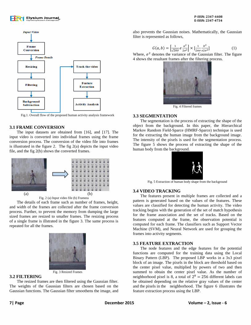
Fig.1. Overall flow of the proposed human activity analysis framework
3.1 FRAME CONVERSION The input datasets are obtained from [16], and [17]. The
input video is converted into individual frames using the frame
conversion process. The conversion of the video file into frames
is illustrated in the figure 2. The fig 2(a) depicts the input video
file, and the fig 2(b) shows the converted frames.
(a) (b)
Fig. 2 (a) Input video file (b) Framess
The details of each frame such as number of frames, height,
and width of the frames are collected after the frame conversion
process. Further, to prevent the memory from dumping the large
sized frames are resized to smaller frames. The resizing process
of a single frame is illstrated in the figure 3. The same process is
repeated for all the frames.
Fig. 3 Resized Frames
3.2 FILTERING The resized frames are then filtered using the Gaussian filter.
The weights of the Gaussian filters are chosen based on the
Gaussian functions. The Gaussian filter smoothens the image, and
also prevents the Gaussian noises. Mathematically, the Gaussian
filter is represented as follows,
( ) [
√
]
(1)
Where, denotes the variance of the Gaussian filter. The figure
4 shows the resultant frames after the filtering process.
Fig. 4 Filtered frames
3.3 SEGMENTATION The segmentation is the process of extracting the shape of the
object from the background. In this paper, the Hierarchical
Markov Random Field-Sparce (HMRF-Sparce) technique is used
for the extracting the human image from the background image.
The intensity of the pixels is used for the segmentation process.
The figure 5 shows the process of extracting the shape of the
human body from the background.
Fig. 5 Extraction of human body shape from the background
3.4 VIDEO TRACKING The features present in multiple frames are collected and a
pattern is generated based on the values of the features. These
values are classified for detecting the human activity. The video
tracking begins with the generation of the set of match hypothesis
for the frame association and the set of tracks. Based on the
features computed at the frame, the observation potential is
computed for each frame. The classifiers such as Support Vector
Machine (SVM), and Neural Network are used for grouping the
frames into activity segments.
3.5 FEATURE EXTRACTION The node features and the edge features for the potential
functions are computed for the training data using the Local
Binary Pattern (LBP). The proposed LBP works in a 3x3 pixel
block of an image. The pixels in the block are threshold based on
the center pixel value, multiplied by powers of two and then
summed to obtain the center pixel value. As the number of
neighborhood pixel is 8, a total of different labels can
be obtained depending on the relative gray values of the center
and the pixels in the neighborhood. The figure 6 illustrates the
feature extraction process using the LBP.

P-ISSN: 2347-4408 E-ISSN: 2347-4734
8| Page December 2015 Volume – 2, Issue - 6
Threshold
8 1 1
2 5 8
3 4 9
Binary 1001100
Decimal: 52
1 0 0
0 1
0 0 1
Fig. 6 Feature extraction using the Local Binary Pattern
3.6 Activity Analysis Based on the extracted features, the activity being performed
by human is analyzed. Here, the activity performed by the person
in figure 6 is detected as walking.
4. PERFORMANCE ANALYSIS
The performance of the proposed Neural Network (NN)
classifier is validated against the existing SVM classifier for the
metrics such as,
Accuracy
Precision
Recall
4.1 ACCURACY The accuracy defines the proximity of the measurement
results to the true value. The accuracy of the proposed NN
classifier is computed using the following equation,
( )
(2)
Where,
TP is the number of true positives
TN denotes the number of true negatives
n represents the total population.
Fig. 7 Comparison of accuracy for the existing, and the proposed method
The figure 7 shows the comparison of accuracy for the
proposed NN, and SVM classifier. From the figure it is analyzed
that the proposed NN classifier provides higher accuracy than the
existing SVM classifier.
4.2 PRECISION The precision is defined as the ratio of the true positives and
the sum of true positive, and true negative values. It is computed
using the following equation,
(3)
The figure 8 shows the comparison of the precision for the
various video files. Each iteration in the graph represents an
individual video file. From the graph it is concluded that the
precision value is high for all the iterations.
Fig. 8 Comparison of precision for multiple iterations
4.3 RECALL
P-ISSN: 2347-4408 E-ISSN: 2347-4734
9| Page December 2015 Volume – 2, Issue - 6
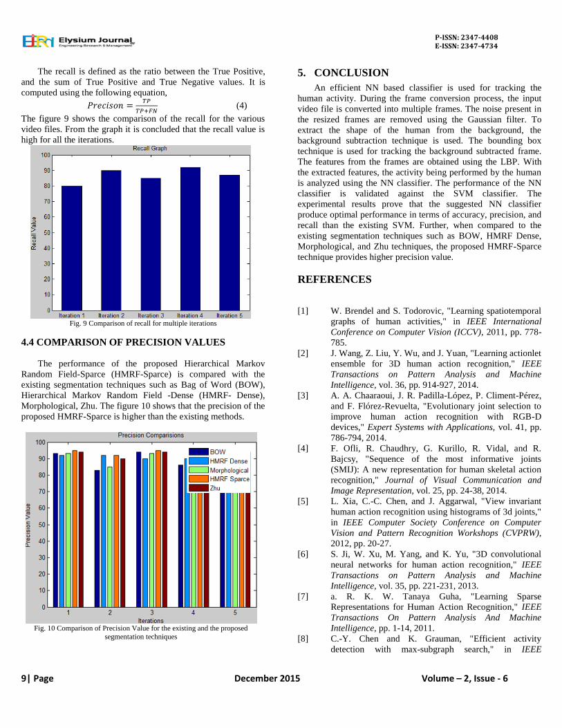
The recall is defined as the ratio between the True Positive,
and the sum of True Positive and True Negative values. It is
computed using the following equation,
(4)
The figure 9 shows the comparison of the recall for the various
video files. From the graph it is concluded that the recall value is
high for all the iterations.
Fig. 9 Comparison of recall for multiple iterations
4.4 COMPARISON OF PRECISION VALUES
The performance of the proposed Hierarchical Markov
Random Field-Sparce (HMRF-Sparce) is compared with the
existing segmentation techniques such as Bag of Word (BOW),
Hierarchical Markov Random Field -Dense (HMRF- Dense),
Morphological, Zhu. The figure 10 shows that the precision of the
proposed HMRF-Sparce is higher than the existing methods.
Fig. 10 Comparison of Precision Value for the existing and the proposed
segmentation techniques
5. CONCLUSION
An efficient NN based classifier is used for tracking the
human activity. During the frame conversion process, the input
video file is converted into multiple frames. The noise present in
the resized frames are removed using the Gaussian filter. To
extract the shape of the human from the background, the
background subtraction technique is used. The bounding box
technique is used for tracking the background subtracted frame.
The features from the frames are obtained using the LBP. With
the extracted features, the activity being performed by the human
is analyzed using the NN classifier. The performance of the NN
classifier is validated against the SVM classifier. The
experimental results prove that the suggested NN classifier
produce optimal performance in terms of accuracy, precision, and
recall than the existing SVM. Further, when compared to the
existing segmentation techniques such as BOW, HMRF Dense,
Morphological, and Zhu techniques, the proposed HMRF-Sparce
technique provides higher precision value.
REFERENCES
[1] W. Brendel and S. Todorovic, "Learning spatiotemporal
graphs of human activities," in IEEE International
Conference on Computer Vision (ICCV), 2011, pp. 778-
785.
[2] J. Wang, Z. Liu, Y. Wu, and J. Yuan, "Learning actionlet
ensemble for 3D human action recognition," IEEE
Transactions on Pattern Analysis and Machine
Intelligence, vol. 36, pp. 914-927, 2014.
[3] A. A. Chaaraoui, J. R. Padilla-López, P. Climent-Pérez,
and F. Flórez-Revuelta, "Evolutionary joint selection to
improve human action recognition with RGB-D
devices," Expert Systems with Applications, vol. 41, pp.
786-794, 2014.
[4] F. Ofli, R. Chaudhry, G. Kurillo, R. Vidal, and R.
Bajcsy, "Sequence of the most informative joints
(SMIJ): A new representation for human skeletal action
recognition," Journal of Visual Communication and
Image Representation, vol. 25, pp. 24-38, 2014.
[5] L. Xia, C.-C. Chen, and J. Aggarwal, "View invariant
human action recognition using histograms of 3d joints,"
in IEEE Computer Society Conference on Computer
Vision and Pattern Recognition Workshops (CVPRW),
2012, pp. 20-27.
[6] S. Ji, W. Xu, M. Yang, and K. Yu, "3D convolutional
neural networks for human action recognition," IEEE
Transactions on Pattern Analysis and Machine
Intelligence, vol. 35, pp. 221-231, 2013.
[7] a. R. K. W. Tanaya Guha, "Learning Sparse
Representations for Human Action Recognition," IEEE
Transactions On Pattern Analysis And Machine
Intelligence, pp. 1-14, 2011.
[8] C.-Y. Chen and K. Grauman, "Efficient activity
detection with max-subgraph search," in IEEE

P-ISSN: 2347-4408 E-ISSN: 2347-4734
10| Page December 2015 Volume – 2, Issue - 6
Conference on Computer Vision and Pattern
Recognition (CVPR), 2012, pp. 1274-1281.
[9] V. Morariu and L. S. Davis, "Multi-agent event
recognition in structured scenarios," in IEEE Conference
on Computer Vision and Pattern Recognition (CVPR),
2011, pp. 3289-3296.
[10] M. Hoai, Z.-Z. Lan, and F. De la Torre, "Joint
segmentation and classification of human actions in
video," in IEEE Conference on Computer Vision and
Pattern Recognition (CVPR), 2011, pp. 3265-3272.
[11] Q. V. Le, "Building high-level features using large scale
unsupervised learning," in IEEE International
Conference on Acoustics, Speech and Signal Processing
(ICASSP), 2013, pp. 8595-8598.
[12] S. Oh, A. Hoogs, A. Perera, N. Cuntoor, C.-C. Chen, J.
T. Lee, et al., "A large-scale benchmark dataset for event
recognition in surveillance video," in IEEE Conference
on Computer Vision and Pattern Recognition (CVPR),
2011, pp. 3153-3160.
[13] Y. Zhang, X. Liu, M.-C. Chang, W. Ge, and T. Chen,
"Spatio-temporal phrases for activity recognition," in
Computer Vision–ECCV 2012, ed: Springer, 2012, pp.
707-721.
[14] B. Yao, X. Jiang, A. Khosla, A. L. Lin, L. Guibas, and
L. Fei-Fei, "Human action recognition by learning bases
of action attributes and parts," in IEEE International
Conference on Computer Vision (ICCV), 2011, pp.
1331-1338.
[15] Ó. D. Lara, A. J. Pérez, M. A. Labrador, and J. D.
Posada, "Centinela: A human activity recognition system
based on acceleration and vital sign data," Pervasive and
Mobile Computing, vol. 8, pp. 717-729, 10// 2012.
[16] ULCA Department of Statistics. Available:
http://statistics.ucla.edu/
[17] "VIRAT Video Dataset."
P-ISSN: 2347-4408 E-ISSN: 2347-4734
11| Page December 2015 Volume – 2, Issue - 6
DESIGN OF LOW POWER 32-BIT CSKA FOR HIGH SPEED APPLICATIONS
C.Yamini1, M.Krishnamurthy
2
1PG Scholar, PSNA College of Engineering and Technology, Dindigul.
Email id: [email protected]
2Assistant Professor, PSNA College of Engineering and Technology, Dindigul.
Email id: [email protected]
Abstract— Research in Very Large Scale Integration (VLSI) based
design of Integrated Circuits (IC) addresses the issues of power, area
and time consumption by the components used. These violates the
speed of operation in DSP processors. To improve the speed, an
optimized Design is required in such a way that the utilization of
components are less. The inclusion of Multiplier and Accumulator
(MAC) unit in the DSP processor Design performs the number of
operation by using adders. Hence, the reduction in power, area and
time in full adder is the necessary process in low power applications.
Modern DSP processors uses the carry chain for optimization in carry
forwarding path which reduces the delay effectively. The Carry Select
Adder (CSLA) is the prominent solution to improve the speed of
parallel operation. But, the result contains more number of carriers.
Hence, multiplexers are used for selection of required sum output and
associated carry. This paper optimizes the carry forwarding path by
replacing the multiplexers with the Boolean function based gate
construction. Moreover, the employment of carry-skip mechanism
reduces the number of components required to design a 32-bit ripple
carry adder. Besides, the application of Microwind- DSCH tool to
create the layout of corresponding 32 bit adder. The DSCH tool
visualizes the carry forwarding path and the time required to perform
the operation effectively. The optimization provided in adder structure
enhances the operational speed with minimum area occupation and
power consumption.
Index Terms— AND-OR Inverter (AOI), Carry Select Adder (CSLA),
Carry Skip Adder (CSKA), Critical Path delay, OR-AND Inverter
(OAI), Ripple Carry Adder (RCA), Power consumption.
1. INTRODUCTION
An effective use of available hardware is the ultimate objective of
various algorithms development. The efficiency of algorithm
depends on various measures power, area and time consumption.
The hardware performs the primitive set of Boolean and ALU
operations based on the algorithm designing. The determinations
of functions performed on hard logic and soft logic is an
important process in Field Programmable Gate Array (FPGA)
Design. Hardened arithmetic structures are long withstand
compared to soft structures such hard circuits otherwise called as
carry logic. The interaction of adders with the LUTs, Flip Flops
used and the optimal; trade-off between area-power and speed are
the important issues in the design of multi-bit carry adders. The
collective interaction between the computational units achieve the
low error rate and high precision. But, the hardware overhead is
an important problem in the design of hard or carry adders. The
evolution of self-checking Ripple Carry Adders (RCA) optimizes
the hardware overhead considerably.
The more number of critical path reduces the speed of
operation and the gain of transistor depends upon its size. The
proposal of transistor based adders reduces the time consumption
by shortening the critical path and size. The RCA contains the
simple design methods. But, the Carry Propagation Delay (CPD)
is the major problem in RCA. Hence, to overcome the delay issue
two strategies are introduced. They are Carry Look-ahead Adder
(CLA) and Carry Select Adder (CSA). The selection of one out of
each pair in final sum and carry reduces the CPD effectively. The
maximum path propagation consumes more delay. Hence various
strategies such as SQRT-CSLA, CCSLA Binary Excess-1
Converter (BEC), CSLA Common Boolean Logic (CSLA-CBL)
solves the delay problem and makes the design as an attractive
manner.
The analytical evaluation of various CSLA strategies extends
the capability of application of CSLA to binary, decimal adders
and subtractors. Reversible or information lossless systems are an
important requirement in low power CMOS applications. The
direct computation of carry values from adder inputs in carry look
ahead adder overcome the limitations in RCA strategies. The
reversible implementation in CLA optimized the number of gates,
quantum cost and delay. The D-latch based CSLA further reduces
the power. The scheduling of carry selection before the
calculation of final sum is different compared to existing carry
selection approaches. The extension of CSLA to Carry Skip
Adder (CSKA) to analyze the power and performance of MAC
designs.
The evolution of carry tree adders enhances the operational
speed with the various bit widths operation 128 and 256 bit. The
presence of fast carry chain in carry tree adders improves the
operational speed by minimizing the delay of RCA and carry skip
adder. The optimization in carry path is the ultimate solution for
delay. Heat dissipation in the components is one of the constraint
for CSKP adder design which originates the reversible logic
implementation. The introduction of reversible logic gate called
‘Inventive0gate’ synthesizes the adder modules to minimize the
gate count and outputs. The application of reversible logic
extends into the construction of quantum computation, nano-
technology low power digital circuits. The design of carry skip
BCD adder by using the reversible logic to minimize the number
of gates and outputs. Several reversible based BCD adder
strategies introduced in research work for low power digital
circuits. From the study, it is observed that, the reduction of gate

P-ISSN: 2347-4408 E-ISSN: 2347-4734
12| Page December 2015 Volume – 2, Issue - 6
count, power consumption and area occupation are the major
constraints to design the optimal VLSI circuits. This paper
proposes the modified strategy of CSKA by replacing the
multiplexers by the Boolean function minimization based logic
gates which optimizes the critical path delay and improve the
speed of operation.
The technical contributions of proposed layout design of 32 bit
Carry Skip Adders (CSKA) listed as follows:
The proposal of optimized strategy in implementation logic in
RCA reduces the critical path delay.
The achievement of reduction of gate count and power
consumption by proposed CSKA.
The extensive visualization of layout framework for 32 bit
CSKA using Microwind-DSCH tool.
The rest of the paper is organized as follows. Section II
presents a description about the previous research works which is
relevant to the optimal adder Designs. Section III involves the
detailed description about the proposed layout framework for
optimized 32-bit Carry Skip Adder. Section IV presents the
comparative analysis between proposed and existing methods on
network parameters. This paper concludes in Section V.
2. RELATED WORK
This section describes the various related adder Designs and
the optimization methodologies for the improvement in
operational speed. High speed and low power digital circuits are
an attractive research area in DSP processors. Multiply
Accumulator (MAC) unit is the basic element in low power
circuits. The working of hardware governed by algorithms
developed by the user. Gurjar et al constructed the high speed
adder circuit by using the Hardware Description Language (HDL)
[1]. The brief analysis about the synthesis and simulation were
presented and the application of HDL for the design of high speed
circuits. The hardened adder circuits or carry based adder
evaluated the performance on various micro-benchmark circuits
and small designs. Luu et al extended the utilization of hardened
adder circuits in larger bench mark designs with the carry chain
mechanism [2]. During larger benchmark circuits implementation,
the interactions among the analog computational units was made
to achieve the low error rate and high precision. Woo et al
presented how the moderate interactions among the analog units.
The minimization of error and the achievement of high precision
provided [3]. But, the optimization in power and delay were
required. The integration among the components was the
important requirement for high speed arithmetic blocks. Francis
et al introduced the bypassing technique and modification in
adder Design in multiplier to optimize the power and delay. They
developed different logic style adders for high speed MAC unit
[4]. The speed of operation dependent on the critical path in
which the carry ripples through it. For the longest critical path,
the speed is low. Jain et al presented the area efficient transistor
based adders that shortened the critical path thereby delay
minimization was achieved[5]. The evolution of multi-standard
wireless receivers, portable and mobile devices requires an
optimized Design for area-delay and power minimization.
The improvement in performance of DSP processors provided
by an efficient adder design. Ripple Carry Adder (RCA) was the
simple design strategy in adder Design. But, the propagation of
carry consumed more time called Carry Propagation Delay
(CPD). The evolution of Carry Selection Adders (CSLA) reduced
the CPD effectively. Mohanty et al eliminate the redundant logic
operations of traditional CSLA and formulated the logic by
scheduling of carry selection process. The introduction of logic
optimization unit provided in carry selection unit [6] offered the
less delay and power. But, the gate count was high which
occupied large space. Sreenivasulu et al used the gate level
modification scheme to traditional CSLA Design significantly
reduced the power and area consumption. The modified version
of CSLA called as Square-Root CSLA (SQRT CSLA) [7].
Saranya extended the SQRT CSLA to 8, 16, 32 and 64 bit square
root operations [8]. But, the extension of CSLA to decimal adder
was not suitable due to the occurrence of incorrect carry bits.
Saxena et al introduced the gate-level modification to
conventional CSLA reduces the delay, power consumption. The
modifications were tested on several bit wise operations. The
comparison of modified CSLA [9] with the conventional
structures also presented. Dorrigiv et al computed the pairs of
corrective carry out bits according to decimal operations [10]. The
selection of corrected pairs by the carry-out bits and the inclusion
of carry-in bits in addition process achieved the optimal
consumption in area and delay. The study of data dependency and
the identification of redundant operations were important in the
implementation of CSLA.
Shirisha et al scheduled the carry selection process prior to
calculation of final sum [11]. The utilization of bit patterns in
carry words and the fixed Cin bits provided a logic optimization
in carry selection and generation units. The conventional CSLA
adder Designs dissipated the maximum power by lose of bits
information. The raise up of reversible logic in which unique map
between the input and output vectors achieved. Jamal et al
presented the reversible implementations on carry look ahead
adder to overcome the limitations in conventional CSLA by direct
computation of carry values from adder inputs [12]. A high speed
and low power consumption are the important factors in the
design of CSLA. Patnayak et al proposed D latch based CSLA
which was the extension of traditional CSLA to further reduce the
power consumption [13]. The scheduling of carry selection before
the calculation of final sum reduced the power consumption.
Reversibility prevented the energy dissipation and bit error by the
introduction of fault tolerant mechanism. Mitra et al presented the
detailed design of Reversible Fault Tolerant-Full Adder (RFT-
FA) [14] with the minimum quantum cost. The merging of
minimization of gates and garbage outputs in RFT based Carry
Look-ahead Adders (CLA) provided. The creation of area
efficient and low power high speed MAC unit comprised Carry
Skip Adders (CSKA). Hence, the research works turn to CSKA
Design and the optimization in CSKA. Kalaiselvi et al further
reduced the power consumption and improved the operational
speed [15]. The comparison of power consumption and
performance analysis between the proposed and existing methods
conveyed the suitability of CSKA in future MAC designs.
P-ISSN: 2347-4408 E-ISSN: 2347-4734
13| Page December 2015 Volume – 2, Issue - 6
Bhagyalakshmi et al extended the applicability of reversible
logic to the Binary Coded Decimal (BCD) [16] to optimize the
quantum computational cost. The computational structures
introduced the high loss of information if the large bit sizes were
introduced. Ali et al developed the new reversible logic gates
called FHNG gate [17] which reduced the loss of information for
large size bit operations. Rajmohan et al improved the design
parameters gate count, area and power by the integration of
reversible mechanism with the CSKA [18]. The raise of some
problems during the integration of DSP processors with the
quantum computers. Shukla et al designed the low power
arithmetic and data path units by using the reversible logic
implementation in Carry Look-ahead Adder (CLA) [19]. The
investigation about the delay performance with the evolution of
carry tree adders was an important research area. Cury et al
discussed the design of fastest type adders by the application of
carry chain in traditional RCA [20] and support the minimum
delay performance for various bit sizes ranging from 128 to 256
bit. The heat dissipation by the components was more. Hence,
Misra et al introduced the reversible logic gate called
Inventive0gate [21] which was an efficient and optimized design
Design in order to reduce the gate count. Thereby, the
minimization of heat dissipation achieved. But, this paper
modifies the traditional structure of CSKA by replacing the
multiplexers by the Boolean function based gate minimization
further reduces the gate count, area and power consumption.
Moreover, the design of 32-bit CSKA structure by the Microwind
DSCH tool investigated.
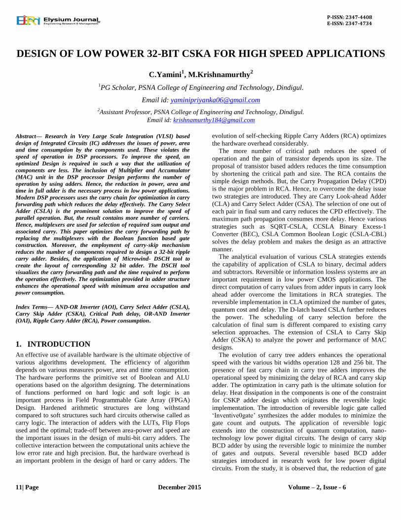
3. OPTIMAL 32-BIT CARRY SKIP ADDER
VISUALIZATION
This section presents the visualization of optimal 32 bit Carry
Skip Adder (CSKA) by replacement of multiplexers in
Microwind-DSCH environment. The minimization of critical path
delay provided by using Boolean function gate minimization. The
Design for proposed optimal 32-bit adder Design is shown in fig.
1.
Fig. 1 Design of proposed optimal 32-bit adder
The Design of proposed work comprises basic half adders and
full adders, sequence of 32-bit Carry Skip Adder (CSKA) in
DSCH2 environment. The proposed CSKA Design is similar to
conventional CSKA with the difference introduced in incremental
block where the multiplexers are replaced by the Boolean
function based gate minimization. The proposed CSKA is shown
in fig. 2.

P-ISSN: 2347-4408 E-ISSN: 2347-4734
14| Page December 2015 Volume – 2, Issue - 6
Fig. 2 CSKA Design.
The proposed CSKA contains the sequence of 4-bit Ripple Carry
Adder (RCA), AOI-OAI logic and the modified incrementation
block. The table I describes the notations used in proposed work.
Table 1 Notations and descriptions
Symbol Description
Full Adder (FA) stage
Ripple Carry Adder (RCA) stage
Intermediate sum
Final sum
Level of intermediate results
Propagation delay of carry output of FA
Propagation delay of skip logic
Propagation delay of AND gate
Propagation delay of OR gate
Propagation delay of AND-OR-Inverter
logic
Propagation delay of OR-AND-Inverter
logic
Delay of critical path
The detailed description of each block and the functions
performed by using these blocks are as follows:
3.1 CARRY SKIP ADDER
The proposed Carry Skip Adder (CSKA) contains N-cascaded
Ripple Carry Adders in which Full Adders (FA) are included with
the worst propagation delay during the summation of two N-bit
numbers. Depends upon the whether RCA or group of RCA in
propagation mode, the propagation delay also varied in two cases
as follows:
Case i: All FAs are in propagation mode
Let us consider the two N-bit numbers and . The
propagation delay for this case is defined by,
(1)
This equation defines the linear relationship of propagation
delay with numbers is called worst case delay.
Case ii: Group of cascaded FAs in propagation mode
The carry output of single Full Adder (FA) chain is equal to
carry input of another FA chain.
The critical path of each CSKA contains three parts and the
description about these paths and associated delay is defined as
follows:
The path of the first stage of FA in CSKA
The path of intermediate carry skip stage
The path of the last stage in FA chain.
The increase in adder stages will increase the critical path for
carry propagation. Thereby, the operational speed is less with the
maximum gate count. To optimize the critical path delay, the
modification of conventional CSKA Design is provided with the
carry skip logic, AOI-OAI logic and modified incrementation
block.
3.2 AOI-OAI LOGIC
The replacement of multiplexers with the AND-OR-Inverter
(AOI) and OR-AND-Inverter (OAI) logic gates that contains
small number of transistors with the lower delay and power and
area consumption. The propagation of carry through the skip
logics is complemented. Hence, the generation of complement of
carry at the even stages of skip logics. The power consumption by
AOI-OAI logic is less compared to the conventional Design.
Due to the presence of the inverting functions in standard cell
libraries of AOI-OAI, they are utilized instead of multiplexers in
order to reduce the power and area consumption. The alternative
utilization of AOI-OAI in such a way that, if one skip logic uses
AOI, then the next skip logic uses OAI increases the critical path
delay considerably. This is because of the fact that the CSKA
with AOI-OAI does not have the capability to bypass the zero
carry input. To overcome this problem, the zero carry input to the
RCA is implemented. This implementation leads to no need to
wait for carry propagation from previous RCA stage and the
parallel computation of carries effectively reduces the
unnecessary time consumption.
3.3 MODIFIED INCREMENTATION BLOCK
The optimal CSKA contains RCA with an additional block
called modified incrementation block. The carry input to RCA
blocks except first RCA is zero which provides the simultaneous
execution of addition operation. In the proposed structure the first
block computes the sum and carry and the other blocks are
simultaneously computes the intermediate results.
The first stage (0) in proposed Design contains RCA only and
the stage 1 to Q contains two modules namely, RCA and modified
incrementation block. The modified incremental block contains
chain of Half Adders (HA) as shown in fig. 3.
Fig. 3 Incrementation Structure
The incrementation block produces the number of intermediate
results up to the level defined by,
∑ (2)
The considerable reduction of delay provided with the
consideration of carry output generated in overall Design rather
than the carry output of incrementation stage.
From fig. 2, the carry output of Qth
stage is obtained on the
basis of intermediate results and carry output of previous stage
and the carry output of RCA stage . If is one, then

P-ISSN: 2347-4408 E-ISSN: 2347-4734
15| Page December 2015 Volume – 2, Issue - 6
is also one. For is zero, then check whether the product of
intermediate results is one, then the output is same as .
The implementation of optimal 32-bit CSKA Design using
DSCH2 software tool and the simulated output is shown in fig. 4.
3.4 VISUALIZATION OF LAYOUT OF 32-BIT CSKA
The performance of time and critical path is evaluated using the
physical description level. The software that is used to design and
simulate the integrated circuits in physical level is Microwind.
The unification in schematic entry, extraction of schematic, the
layout compilation and mixed circuit simulation provided by
Microwind. The single key based simulation and the command
based editor in Microwind helps to extract the electrical circuit
and performed the analog simulation with the voltage and current
values with the time values.
The command based visualization of various characteristics of
nMOS and pMOS achieved in this tool. The changes in size and
associated parameters changed the voltage and current values.
Two important tools are used for validation of design. They are
process simulator and logic cell compiler. Once the fabrication is
completed, the first one shows the vertical perspective of layout.
The sophisticated tool that enables the automatic design of CMOS
circuit. The Verilog based description is provided by using the
combination of user friendly schematic editor called DSCH with
the logic simulator. The rules required for the design and
fabrication are arranged in the cell. The 3 D visual layout for
proposed optimal 32 bit Design is shown in fig. 5.
Fig. 4 Simulated Design
Fig. 5 3D layout of proposed 32-bit CSKA Design.
P-ISSN: 2347-4408 E-ISSN: 2347-4734
16| Page December 2015 Volume – 2, Issue - 6
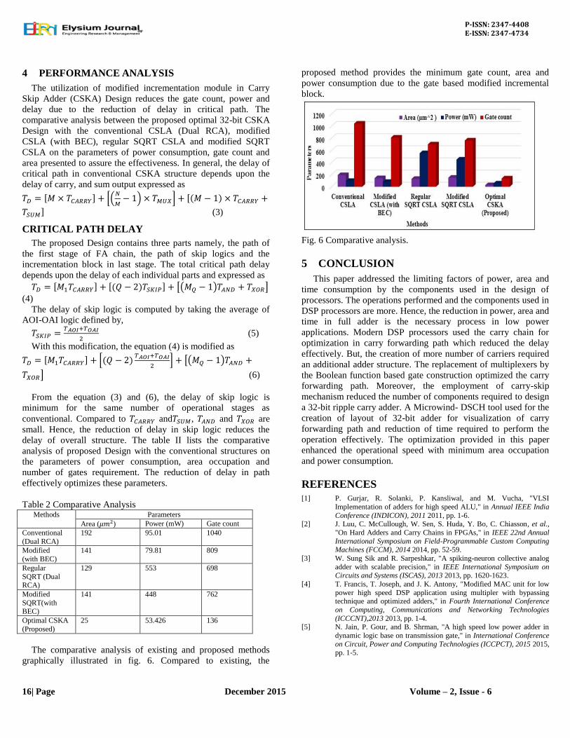
4 PERFORMANCE ANALYSIS
The utilization of modified incrementation module in Carry
Skip Adder (CSKA) Design reduces the gate count, power and
delay due to the reduction of delay in critical path. The
comparative analysis between the proposed optimal 32-bit CSKA
Design with the conventional CSLA (Dual RCA), modified
CSLA (with BEC), regular SQRT CSLA and modified SQRT
CSLA on the parameters of power consumption, gate count and
area presented to assure the effectiveness. In general, the delay of
critical path in conventional CSKA structure depends upon the
delay of carry, and sum output expressed as
[ ] *(
) + [
] (3)
CRITICAL PATH DELAY
The proposed Design contains three parts namely, the path of
the first stage of FA chain, the path of skip logics and the
incrementation block in last stage. The total critical path delay
depends upon the delay of each individual parts and expressed as
[ ] [ ] [( ) ]
(4)
The delay of skip logic is computed by taking the average of
AOI-OAI logic defined by,
(5)
With this modification, the equation (4) is modified as
[ ] *
+ [( )
] (6)
From the equation (3) and (6), the delay of skip logic is
minimum for the same number of operational stages as
conventional. Compared to and , and are
small. Hence, the reduction of delay in skip logic reduces the
delay of overall structure. The table II lists the comparative
analysis of proposed Design with the conventional structures on
the parameters of power consumption, area occupation and
number of gates requirement. The reduction of delay in path
effectively optimizes these parameters.
Table 2 Comparative Analysis Methods Parameters
Area ( ) Power (mW) Gate count
Conventional
(Dual RCA)
192 95.01 1040
Modified
(with BEC)
141 79.81 809
Regular
SQRT (Dual RCA)
129 553 698
Modified
SQRT(with BEC)
141 448 762
Optimal CSKA
(Proposed)
25 53.426 136
The comparative analysis of existing and proposed methods
graphically illustrated in fig. 6. Compared to existing, the
proposed method provides the minimum gate count, area and
power consumption due to the gate based modified incremental
block.
Fig. 6 Comparative analysis.
5 CONCLUSION
This paper addressed the limiting factors of power, area and
time consumption by the components used in the design of
processors. The operations performed and the components used in
DSP processors are more. Hence, the reduction in power, area and
time in full adder is the necessary process in low power
applications. Modern DSP processors used the carry chain for
optimization in carry forwarding path which reduced the delay
effectively. But, the creation of more number of carriers required
an additional adder structure. The replacement of multiplexers by
the Boolean function based gate construction optimized the carry
forwarding path. Moreover, the employment of carry-skip
mechanism reduced the number of components required to design
a 32-bit ripple carry adder. A Microwind- DSCH tool used for the
creation of layout of 32-bit adder for visualization of carry
forwarding path and reduction of time required to perform the
operation effectively. The optimization provided in this paper
enhanced the operational speed with minimum area occupation
and power consumption.
REFERENCES
[1] P. Gurjar, R. Solanki, P. Kansliwal, and M. Vucha, "VLSI
Implementation of adders for high speed ALU," in Annual IEEE India
Conference (INDICON), 2011 2011, pp. 1-6. [2] J. Luu, C. McCullough, W. Sen, S. Huda, Y. Bo, C. Chiasson, et al.,
"On Hard Adders and Carry Chains in FPGAs," in IEEE 22nd Annual
International Symposium on Field-Programmable Custom Computing Machines (FCCM), 2014 2014, pp. 52-59.
[3] W. Sung Sik and R. Sarpeshkar, "A spiking-neuron collective analog
adder with scalable precision," in IEEE International Symposium on
Circuits and Systems (ISCAS), 2013 2013, pp. 1620-1623.
[4] T. Francis, T. Joseph, and J. K. Antony, "Modified MAC unit for low
power high speed DSP application using multipler with bypassing technique and optimized adders," in Fourth International Conference
on Computing, Communications and Networking Technologies
(ICCCNT),2013 2013, pp. 1-4. [5] N. Jain, P. Gour, and B. Shrman, "A high speed low power adder in
dynamic logic base on transmission gate," in International Conference
on Circuit, Power and Computing Technologies (ICCPCT), 2015 2015, pp. 1-5.

P-ISSN: 2347-4408 E-ISSN: 2347-4734
17| Page December 2015 Volume – 2, Issue - 6
[6] B. K. Mohanty and S. K. Patel, "Area–Delay–Power
Efficient Carry-Select Adder," IEEE Transactions on Circuits and Systems II: Express Briefs, vol. 61, pp. 418-422, 2014.
[7] P. Sreenivasulu, K. S. Rao, M. Reddy, and A. V. Babu, "Energy and
Area efficient Carry Select Adder on a reconfigurable hardware," International Journal of Engineering Research and Applications, vol.
2, pp. 436-440, 2012.
[8] K. Saranya, "Low Power and Area-Efficient Carry Select Adder," International Journal of Soft Computing and Engineering (IJSCE)
ISSN, pp. 2231-2307, 2013.
[9] P. Saxena, U. Purohit, and P. Joshi, "Analysis of Low Power, Area Efficient & High Speed Fast Adder," International Journal of
Advanced research on Computer and Communication Engineering,
2013. [10] M. Dorrigiv and G. Jaberipur, "Low area/power decimal addition with
carry-select correction and carry-select sum-digits," VLSI Journal, vol.
47, pp. 443-451, 9// 2014. [11] K. Shirisha and D. S. Rao, "Area-Delay-Power Efficient Carry-Select
Adder," 2015.
[12] L. Jamal, M. Shamsujjoha, and H. H. Babu, "Design of optimal reversible carry look-ahead adder with optimal garbage and quantum
cost," International Journal of Engineering and technology, vol. 2, pp.
44-50, 2012. [13] S. K. Patnayak, M. Raja, and D. Sailaja, "Design Carry Select Adder
With D-Latch," 2015.
[14] S. K. Mitra and A. R. Chowdhury, "Minimum Cost Fault Tolerant Adder Circuits in Reversible Logic Synthesis," in 25th International
Conference on VLSI Design (VLSID), 2012 2012, pp. 334-339. [15] K. Kalaiselvi and H. Mangalam, "Area Efficient High Speed and Low
Power MAC Unit," International Journal of Computer Applications,
vol. 67, pp. 40-44, 2013. [16] H. Bhagyalakshmi and M. Venkatesha, "Optimized design of BCD
adder and Carry skip BCD adder using reversible logic gates,"
International journal on computer science and Engineering, vol. 3, pp. 1439-1449, 2011.
[17] M. S. R. Md.Belayet Ali, Tahmina Parvin, "Optimized Design of Carry
Skip BCD adder using new FHNG reversible logic gates," International Journal of Computer Science, vol. 9, p. 3, 2012.
[18] M. Rajmohan and D. S. Lenin, "A Novel Design of Carry Skip BCD
Adder using Reversible Gates," International Journal of Computer Applications, vol. 73, pp. 46-51, 2013.
[19] S. Shukla, T. Verma, and R. Jain, "Design of 16 Bit Carry Look Ahead
Adder Using Reversible Logic," International Journal of Electrical, Electronics and Computer Engineering, vol. 3, pp. 83-89, 2014.
[20] C. Cury and M. Nisanth, "Design of Parallel Prefix Adders using
FPGAs," IOSR Journal of VLSI and Signal Processing, vol. 4, pp. 45-51, 2014.
[21] N. K. Misra, M. K. Kushwaha, S. Wairya, and A. Kumar, "Cost
efficient design of reversible adder circuits for low power applications," arXiv preprint arXiv:1509.04618, 2015.

P-ISSN: 2347-4408 E-ISSN: 2347-4734
12| Page December 2015 Volume – 2, Issue - 6
HIGH SPEED AND LOW POWER CMOS TECHNOLOGY BASED RAM-CAM
MEMORY DESIGN
K.Vidhya kamu1
and Mr.P.Karthikeyan2
1Applied electronics, PSNA College of Engineering & Technology, Dindigul, Tamil Nadu, India. [email protected]
2PSNA College of Engineering & Technology, Dindigul, Tamil Nadu, India.
Abstract— Content-Addressable Memory (CAM) is a special type of
memory, which is used in very-high speed searching applications. The
other names of CAM are the associative memory, associative storage
and the associative array, which is used for retrieving the contents with
high speed based on the address. We proposed an XOR based content
addressable memory with 8 transistors. The energy consumed by the
proposed CAM design was lowered, when compared to the
conventional low-power CAM design. The proposed method is used to
design the Complementary Metal Oxide Semi Conductor (CMOS)
technology based RAM-CAM memory architecture. The Euclidean
distance based matching is used for comparing and retrieving the
contents in the CAM based memory. The proposed CMOS technology
is used to reduce the leakage power and the delay time in the
transistors. The speed of the proposed method is increased by using the
CAM method in searching and retrieving the content based on the
address. The parameters considered for the design are energy, power,
and the time.
Index Terms—Content-Addressable Memory (CAM), Random Access
Memory (RAM), Complementary Metal Oxide Semi Conductor
(CMOS), Transistors.
1. INTRODUCTION
The Very Large Scale Integration (VLSI) design is the process of
creating an Integrated Circuit (IC). The thousands of transistors
are combined into a single chip. Before the introduction of VLSI
technology the IC’s have a limited set of functions to perform.
The electronic system consists of a CPU, RAM, ROM and other
glue logic. The CMOS technology is used for the construction of
the integrated circuits. The CMOS technology is used in the
following devices such as:
Microprocessors
Microcontrollers
Static RAM
Digital logic circuits
There are two important characteristics of CMOS devices
such as: (1) The CMOS devices are immune to noise and (2) it
consumed less power.
Content addressable memory (CAM) is a special type of
solid-state memory, which accesses the data by their contents
rather than the physical locations. The data to be searched is
compared in parallel against the stored entries. Each and every
entry is associated with the tag to find the perfect match, which is
used in the comparison process. The Random Access Memory
(RAM) is the computer memory, which is accessed randomly.
Ram is the common type of memory, which is found in several
computers and other devices such as the printers. There are two
types of RAM, they are: (1) Dynamic Random Access Memory
(DRAM) and (2) Static Random Access Memory (SRAM).
Fig 1. Typical Structure of the 4x4 CAM
Fig 1 described the typical structure of CAM . The CAM
array is divided into several equal sized sub-blocks, which is
activated independently. The sub-blocks are activated and the
input tag is compared with the few entries of the sub-blocks,
while the rest of the sub-blocks are deactivated. From Fig.1 it is
clear that the input tag is 1100 and the sub-blocks are searched
and outputs the third sub-block.
The existing system used 7-T NAND logic gate for the CAM
cell design. The Match Line (ML) is analyzed and the ML is
combined with the RAM. There are several approaches in the
existing systems such as: (1) NOR based ML, (2) NAND based
ML. The disadvantages of the existing system are:
The CAM consumed more power for
processing
It has complex circuit design
It has high delay time
The bit comparison is performed using the NAND based logic as
a part of the Match-line circuitry. The structure of the NAND
type is identical except for the position of the ML transistors. The

P-ISSN: 2347-4408 E-ISSN: 2347-4734
13| Page December 2015 Volume – 2, Issue - 6
NAND type structure incorporates the significant delay. The
delay is found to be around 12 ns for the matching process. The
TCAM was used normally for the design of high-speed look up
intensive applications such as forwarding and classification of
SRAM. The remainder of the paper is systematized as follows,
Section II describes the literature review related to the low power
CMOS technology and CAM based memory design. Section III
illustrates the proposed architecture, and section IV describes the
performance analysis of the proposed method. Section V
illustrates the conclusion and future work of this paper.
2. RELATED WORK
This section illustrates the literature review related to the
low power CMOS technology and CAM based memory design.
Jarollahi, et al [1] proposed a low-power content addressable
memory (CAM) for employing the associativity between the
input tag and the address of the output data. The proposed method
was based on the sparse clustered network, which eliminated the
parallel comparisons performed during the search. Yang, et al [2]
proposed a Pai-Sigma matchline scheme to reduce the search
power of the Ternary Content Addressable Memory (TCAM).
The NAND-NOR Matchline scheme was used to address the
issues related to the charge sharing and the DC path. The 0.18µm
CMOS technology was used to reduce the power consumed by
the TCAM. Jarollahi, et al [3] proposed a sparse clustered neural
network for achieving the optimal efficiency and large diversity.
The parallel hardware implementation of Gripon-Berrou Neural
Network (GBNN) was introduced in the proposed method. The
proposed architecture was used in the applications of Data
Mining and was embedded inside the processor chips to
communicate with the memory units. Do, et al [4] introduced the
parity bit, which leads to 39% of delay reduction in sensing and
1% power overhead. The peak and the average power
consumption was reduced by the proposed gated-power
technique. Onizawa, et al [5] introduced a reordered overlapped
search mechanism for achieving a high-throughput and low-
energy CAM. A word circuit was divided into two sections that
were sequentially searched to lower the power dissipations.
Gripon and Berrou [6] introduced the two codes called the thrifty
code and the clique code, which were the sub-families of binary
constant weight codes. The sparse neural networks achieved an
optimal performance. In order to achieve an optimal performance
the two codes were introduced. Jarollahi, et al [7] introduced a
Clustered Neural Network (CNN), which stored numerous
messages than the traditional Hopfield Neural Network (HNN).
The hardware architectures for such memories were also
proposed. Peti, et al [8] presented a new hybrid scheme called the
RAM-CAM register renaming scheme. The RAM-CAM scheme
combined both the functionalities of the RAM and CAM
registers. The power dissipated by the CAM renaming scheme
was between 17% and 26% and consumed less energy than the
RAM-based renaming scheme. Jarollahi, et al [9] proposed a
new hardware architecture based on the Sparse Clustered
Networks (SCN) and the method known as Selective Decoding
SCN (SD-SCN). The proposed architecture were suitable for
implementations with low retrieval latency, but were limited to
small networks. Do, et al [10] proposed an efficient power ML
sensing technique, which achieved a low power consumption.
The fully parallel match line structure was introduced with an
Automated Background Checking scheme (ABC). The two
dummy rows were used by the ABC scheme. Wong, et al [11]
compared the Field Programmable Gate Array (FPGA) and the
custom CMOS. The delay and the area of a comprehensive set of
processors were implemented on the custom CMOS and FPGA.
Gripon, et al [12] introduced a low power CAM for employing a
new mechanism for providing the associativity between the input
tags and the address of the output data. The proposed architecture
was based on the clustered sparse network. 0.13µm CMOS
technology was used to reduce the power consumed by the
CMOS technology. The NAND based architecture with higher
number of transistors were constructed. Ullah, et al [13]
presented a novel memory architecture called the hybrid
partitioned Static Random Access (SRAM) memory based
ternary CAM. The TCAM has disadvantages such as low bit
density and high cost per bit. Zhang, et al [14] presented a design
of NOR-type CAM based on the Domain Wall (DW) motion in
magnetic tracks. The CMOS switching and sensing circuits were
shared globally to optimize the cell area. The CMOS 65 nm was
used to evaluate the high performance. Liu, et al [15] proposed
the first packet classification scheme, which used the Binary
CAM (BCAM). The BCAM was similar to the TCAM but every
bit has only two possible states such as 0 or 1. Number of
optimizations techniques were also proposed including the skip
lists, free expansion.
3. PROPOSED METHOD
This section elaborates the proposed CMOS based
Random Access Memory (RAM)-Content Addressable Memory
(CAM) design. The overall flow of our proposed work is depicted
in the Fig 2. It has the following components,
SRAM CMOS Design
CAM CMOS Design
SCAN based enable Function
ML Sense Amplifier
The input bit to be searched is given as input to the
SRAM data register memory. The 6T is used for the SRAM
design of the data register. The condition is checked and if the
RAM data is equal to the CAM data, then the match line is
enabled using the clock. The performance of the input is
analyzed. The CAM array has a group of cell and it is based on
the SCN based MLSA function. The CAM array cell consists of
the following:
Bit line inputs
CAM cell design based on the XOR
Write and read content data.

P-ISSN: 2347-4408 E-ISSN: 2347-4734
14| Page December 2015 Volume – 2, Issue - 6
Fig 2. Proposed CMOS technology based RAM-CAM memory design
3.1 SRAM CMOS DESIGN
Static Random Access Memory (SRAM) is the Random
Access Memory (RAM), which retains the data in the memory as
long it is being supplied with the power. The SRAM is the
volatile type of memory. SRAM does not need to be refreshed
periodically. The cache memory is designed using the SRAM
technique. The 6T based SRAM CMOS design is first designed.
The design was constructed to store the single bit value based on
the bit line and he write line input. The design consists of two
inverter cross connection. The two inverter cross connection is
used for maintaining the given input data. The write line is set to
1 for getting the data from the cross inverter circuit connection.
3.2 CAM CMOS DESIGN
The Complementary metal-oxide semiconductor (CMOS) is
the semiconductor technology, which is used in the transistors.
Several microchips developed for the computers are using the
CMOS technology. In CMOS technology two types of transistors
are used such as: the positive type transistors (P-type Transistors)
and the negative type transistors (N-type Transistors). The 8T
XOR CAM CMOS design is constructed and is shown in Fig.3.
The design consists of the two control line such as the Selection
line and the Bit line for controlling the CAM cell. This process is
used to find the address bit location and the address bit location is
used to check the address level. The logic function is evaluated
and applied to check the address level. The CAM block operates
using the self timed control and an input controller. The CAM
CMOS block contains the CAM block to operate in the timed
manner and controlled manner.
3.3 SCAN BASED ENABLE FUNCTION
The SCAN based enable function is used for finding the
CAM cell array result. The Scan based enable function is used to
apply for the CAM and RAM data. The XOR gate is used for
matching the SRAM data and the CAM data. The XOR gate is
also used for inverting the activation results. The row values in

P-ISSN: 2347-4408 E-ISSN: 2347-4734
15| Page December 2015 Volume – 2, Issue - 6
the CAM data are used for the registration of the input data bit.
Then it is used for activating the ML function.
3.4 ML SENSE AMPLIFIER
The Match Line (ML) amplifier has single energy
storage element ant it is considered as a first order system. The
ML scheme is used for saving the current and it has an active feed
back. The Match Line amplifiers are used check the CAM data
register and the RAM data register value. The clock function is
used to control the output of the matched line row and to get the
address of the contents. The CAM cell array is mainly focused on
the matched line process.
In the proposed system, the CAM is a XOR logic gate
based cell design. The ML sense amplifier is used for the data
matching process. The proposed system processes the data and
searches the data with high speed. The classifiers are constructed
using the proposed architecture. The scale based enable process is
used for finding the CAM cell array result. The XOR gate
function is used to match the SRAM data and the CAM data and
the results are inverted using the XOR based gate function. The
ML sense amplifiers are used check the CAM data registers. The
clock function is used for controlling the output matched row to
retrieve the content address. The advantages of the proposed
methods are:
The power consumed by the CAM is less
The design of the circuit is simple.
The selection process is very fast.
It is accurate that the existing methods
The distance is computed with high efficiency
using the Euclidean distance based matching.
Fig 3. Proposed Circuit Design using the XOR gate.
4. PERFORMANCE ANALYSIS
The performance of the proposed RAM-CAM memory
design is compared with the existing NAND or NOR type CAM
cell with the following metrics such as:
Processing Area
Power Consumption
Delay Time
4.1 PROCESSING AREA
The proposed RAM-CAM design totally reduced the
size of the IC chip. The IC chip consists of several transistors
involved in the design. If the transistor occupied more space, then
the overall circuit is complicated. Hence, the area in the proposed
method should be reduced. To reduce the area occupied by the
single transistor the below formula is used. The area is calculated
using the formula:
(1)
Where, LS denotes the length denotes the length of the single
transistor and the total denotes the whole number of transistors
used in the proposed RAM-CAM circuit. If the area of the single
transistor is reduced, then the whole area in the circuit design is
reduced. The area occupied by the transistors in the existing
methods is 4.83 mm2. The area is reduced by 0.32 mm
2 in the
proposed RAM-CAM based on the CMOS technology.
4.2 POWER CONSUMPTION
The Power is defined as the ability to do some work. The
amount of work is equivalent to the energy consumed per unit
time. The integral of power is defined by the work performed.
The proposed RAM-CAM design is used to reduce the power
consumption. The existing system consumed the 94 mW power
and the power consumption was reduced by 70 mW. If the area is
reduced, then the power consumption was also reduced by the
proposed method. Fig 4 showed the graph of the input values.
The time is plotted against the power and showed that the
proposed methods achieved very less power, when compared to
the existing methods.

P-ISSN: 2347-4408 E-ISSN: 2347-4734
16| Page December 2015 Volume – 2, Issue - 6
Fig 4. Power Consumption graph
4.3 DELAY TIME
The delay time in the proposed method is reduced by the
proposed RAM-CAM method. The delay time in the existing
methods is high. So, the delay time should be decreased in the
proposed system. The delay time achieved in the proposed
method is 2.2 ns. The existing method has 7 ns as the delay time.
The delay time was reduced for matching the contents in the
CAM design.
The values of the metrics discussed above are tabulated
and shown in the Table.1. The values for the existing and the
proposed methods are tabulated in the table. From the table, it is
clear that the proposed RAM-CAM method based on the CMOS
technology achieved less power, low area and less delay time
than the existing system.
The graph for the proposed RAM-CAM memory design
is shown in Fig. 5, which depicted the input and output values.
The delay time is plotted against the voltage values. The graph is
plotted with the binary values such as the 0 and 1. The binary
value of 0 is shown by the 0v frequency and the binary value of 1
is shown by the +5v frequency. The five graphs are shown in
Fig.5. The last graph showed input values taken for processing,
which is the binary value 0 or the binary 1. The sample value is
taken for processing is shown in the first graph. The matching
input from the address is retrieved with high efficiency and within
the specified time. The second graph represents the matching line
in the specified address of the memory. The third graph shows the
processing values inside the memory. The binary value 1 is alone
taken for processing ie., the +5v is used in processing the input.
The ML sense amplifiers are used to sense the input values from
the contents of the memory. The contents retrieved from the
memory is at high speed than the traditional CAM methods. The
simulation results are depicted in the graph shown in fig.5. The
screenshot of the proposed RAM-CAM method is taken for the
proposed method.
Fig 5.Voltage vs. Time
Fig. 6. Comparison of the existing and Proposed System
From fig. 6 it is clear that the existing system has less area,
less power consumed and the less delay, when compared to the
existing methods.
Table 1. Comparison table for Existing and the Proposed system
using the metrics
0102030405060708090
100
Area Power Delay Time
SCN-CAM
RAM-CAM

P-ISSN: 2347-4408 E-ISSN: 2347-4734
17| Page December 2015 Volume – 2, Issue - 6
METRICS EXISTING
SYSTEM
PROPOSED
SYSTEM
SUPPLY
VOLTAGE
1.8V 5V
AREA 4.83 mm2 0.320 mm
2
POWER 94mW 70mW
DELAY TIME 7ns 2.2ns
5. CONCLUSION
The RAM-CAM architecture was designed using the
CMOS technology. The performance of the system is compared
to the NOR and the NAND type CAM memory design. The XOR
based CAM is designed with high efficiency. The Cam cell is
designed to lower power. The CAM is suitable for the low-power
applications and for the applications, which required the parallel
look-up operations. The actual data of interest is stored in the
SRAM and the tag is associated with each and every block just
for the reference. The simple and fast updates can be achieved
without retraining the network entirely. The application depends
on the
non-uniform inputs and results in higher power consumptions and
does not affect the accuracy of the final result. The proposed
methods are used in the following applications such as:
CPU processors
ATM machine
Flash memories
Real Time Servers, etc.
REFERENCES
[1] H. Jarollahi, V. Gripon, N. Onizawa, and W. J. Gross,
"Algorithm and architecture for a low-power content-
addressable memory based on sparse clustered
networks," Very Large Scale Integration (VLSI) Systems,
IEEE Transactions on, vol. 23, pp. 642-653, 2015.
[2] S.-H. Yang, Y.-J. Huang, and J.-F. Li, "A low-power
ternary content addressable memory with Pai-Sigma
matchlines," Very Large Scale Integration (VLSI)
Systems, IEEE Transactions on, vol. 20, pp. 1909-1913,
2012.
[3] H. Jarollahi, N. Onizawa, V. Gripon, and W. J. Gross,
"Architecture and implementation of an associative
memory using sparse clustered networks," in IEEE
International Symposium on Circuits and Systems
(ISCAS), 2012, 2012, pp. 2901-2904.
[4] A.-T. Do, S. Chen, Z.-H. Kong, and K. S. Yeo, "A high
speed low power CAM with a parity bit and power-gated
ML sensing," Very Large Scale Integration (VLSI)
Systems, IEEE Transactions on, vol. 21, pp. 151-156,
2013.
[5] N. Onizawa, S. Matsunaga, V. C. Gaudet, W. J. Gross,
and T. Hanyu, "High-Throughput Low-Energy Self-
Timed CAM Based on Reordered Overlapped Search
Mechanism," IEEE Transactions on Circuits and
Systems I: Regular Papers, vol. 61, pp. 865-876, 2014.
[6] V. Gripon and C. Berrou, "Nearly-optimal associative
memories based on distributed constant weight codes,"
in Information Theory and Applications Workshop
(ITA), 2012, 2012, pp. 269-273.
[7] H. Jarollahi, N. Onizawa, V. Gripon, and W. J. Gross,
"Reduced-complexity binary-weight-coded associative
memories," in IEEE International Conference on
Acoustics, Speech and Signal Processing (ICASSP),
2013, 2013, pp. 2523-2527.
[8] S. Petit, R. Ubal, J. Sahuquillo, and P. Lopez, "Efficient
Register Renaming and Recovery for High-Performance
Processors," Very Large Scale Integration (VLSI)
Systems, IEEE Transactions on, vol. 22, pp. 1506-1514,
2014.
[9] H. Jarollahi, N. Onizawa, and W. J. Gross, "Selective
decoding in associative memories based on sparse-
clustered networks," in Global Conference on Signal
and Information Processing (GlobalSIP), 2013 IEEE,
2013, pp. 1270-1273.
[10] A. T. Do, C. Yin, K. S. Yeo, and T. T.-H. Kim, "Design
of a power-efficient CAM using automated background
checking scheme for small match line swing," in
Proceedings of the ESSCIRC (ESSCIRC), 2013 2013,
pp. 209-212.
[11] H. Wong, V. Betz, and J. Rose, "Comparing FPGA vs.
custom CMOS and the impact on processor
microarchitecture," in Proceedings of the 19th
ACM/SIGDA international symposium on Field
programmable gate arrays, 2011, pp. 5-14.
[12] H. Jarollahi, V. Gripon, N. Onizawa, and W. J. Gross,
"A low-power content-addressable memory based on
clustered-sparse networks," in International Conference
on Application-Specific Systems, Architectures and
Processors (ASAP), 2013 IEEE 24th, 2013, pp. 305-308.
[13] Z. Ullah, K. Ilgon, and S. Baeg, "Hybrid partitioned
SRAM-based ternary content addressable memory,"
IEEE Transactions on Circuits and Systems I: Regular
Papers, vol. 59, pp. 2969-2979, 2012.
[14] Y. Zhang, W. Zhao, J.-O. Klein, D. Ravelsona, and C.
Chappert, "Ultra-high density content addressable
memory based on current induced domain wall motion
in magnetic track," IEEE Transactions on Magnetics,
vol. 48, pp. 3219-3222, 2012.
[15] A. X. Liu, C. R. Meiners, and E. Torng, "Packet
classification using binary Content Addressable
Memory," in INFOCOM, 2014 Proceedings IEEE, 2014,
pp. 628-636.

P-ISSN: 2347-4408
E-ISSN: 2347-4734
18| Page December 2015 Volume – 2, Issue - 6
DESIGN AND IMPLEMENTATION OF 32 BIT ALU USING LOOK AHEAD CLOCK
GATING BASED ON FPGA
V. Prasanth (Ph.D.) 1
, M. Sri Manikyamba2
1Head of the Department-ECE, Pragati Engineering College, Surampalem (Ap), India.
2Pragati Engineering College, Surampalem (AP) India. Email id: [email protected]
Abstract: Any type of digital architecture is modified by using
the VLSI technology. In digital systems, clock gating is the
best method to reduce consumption of power. As power
consumption plays an important role in any integrated circuit.
This methodology is mainly used in all type of real world
applications and this technology is to enhance the internal
architecture level. There are 3 gating methods. The most
popularly known gating method is synthesis based.
Unfortunately, the Synthetic based gating method leaves the
majority of the clock pulses driving the flip flops are
terminated. A data driven method halts most of the clock
pulses and produces higher power savings, but its application
is complex and dependent. The Auto-Gated Flip Flops
(AGFF) is the third method which yields moderately lower
power saving. This paper introduces a novel Look-Ahead
Clock Gating (LACG) method which is the combination of all
the three gating methods. It calculates the clock enabling
signals of every flip flops one cycle from this time, which it
depends on the FFs cycle data at present. In a CPU, the most
commonly edited modules is the ALU. During most
instruction executions, it is employed. Therefore, a major
concern in the ALU is the consumption of power. This paper
motivates to reduce the ALU architecture for many digital
applications and to improve the internal process in ALU
architecture with look ahead clock gating approach.
Reduction of delay and power for the data path PE unit in 32
bit ALU architecture.
Keywords: ALU, LACG, Clock gating, dynamic power.
1. INTRODUCTION
In the earlier days, the designers of VLSI were more interested
on the area of the circuits, performance, reliability and cost was
also the main consideration and power consumption was their
minor consideration. Now-a-days, the power is also being given
equal importance in comparison to area and speed. The dynamic
power dissipation is being comparable with both short circuit
and leakage power as technology scale down. To identify and
modify the various leakages and switching of components is
very essential to estimate and also the reduction of power
consumption in high speed and low power applications. Clock
gating is the best method to reduce the power consumption. It is
involved in all levels of system architecture, logic design, block
design and gates. The predefined enabling signals and gating
signal are ANDed. There are three gating methods, first one is
the synthesis based, which enables clock signals based on the
logic of the fundamental system. Unfortunately, it leaves the
majority of the clock pulses driving the flip flops are terminated.
Second is the data driven method which stops most of those
clock pulses and gains higher power savings, but it is application
dependent and the implementation is highly complex. And the
third method is auto gated flip flop. It is simple but gains
relatively small power savings. In synthesis based clock gating,
functional blocks and modules are not needed to be clocked as
the clock enabling signals are well understood the system level.
It can be defined effectively and capture the period. To address
the redundancy from the synthesis based, a data driven clock
gating is proposed for flip flops. If the flip flops state is not
changed to the next clock cycle then the flip flops driven by the
clock signals are disabled. It suffers from a very short time
window where the gating circuitry works correctly. The delay of
the XOR, OR, AND gate and latch need not beyond the setup
time of the flip flop. Another difficulty of data driven clock
gating is its design methodology. The low power look ahead
clock gating method combines all the three gating methods. The
system clock signals is one of the main dynamic power
consumers in computing and electronic products, which is
normally responsible for 30-70 % of the total dynamic switching
power consumption. Several techniques are introduced to reduce
the dynamic power of which clock gating is primary. This look
ahead clock gating calculates the clock enabling signals of every
flip flops one cycle from this time, which it depends on the FFs
cycle data at present. For computing the enable signals and the
propagation, a full clock cycle is allotted for both auto gated and
data driven in order to avoid its tight timing constraints. This
look ahead clock gating method is introduced, based on the auto
gated flip flop. The Comparison of the look ahead, power gating
and data driven clock gating are done in this paper. It shows,
when compared to the data driven, the look ahead consumes less
power and to reduce the power
2. ARCHITECTURE

P-ISSN: 2347-4408
E-ISSN: 2347-4734
19| Page December 2015 Volume – 2, Issue - 6
The ALU architecture mainly used to perform the arithmetic
and logical process and the arithmetic process consists the
adder and subtractor and multiplier architecture. The mux input
section to change the output based on selection process. The
selection process used to modify the output unit architecture.
The ALU block is used to optimize the internal architecture.
The internal architecture to consume the three arithmetic
operations and five logical operations. The buffer architecture
used to store the output with delay time for the ALU operation
and to check the required selection signal .The mux operation
used to find the output and to store the mux input. And to select
the input selection signal and to display the output result.
Figure 1. Block Diagram of ALU Architecture
3. MODULES
3.1 SELECTION MUX ARCHITECTURE
The input bits are to be applying the ALU circuit. The 8:1 mux
architecture is used to select the operation output data bits
based on arithmetic and logical operation. The mux architecture
is consists of overall internal ALU architecture output data bits
and the look ahead clock gating technique is used to optimize
the selection processing time. The mux input section is to
change the output based on selection process. The selection
process is used to modify the output unit architecture.
3.2 ALU ARCHITECTURE
The ALU architecture mainly used to perform the
arithmetic and logical process and the arithmetic process
consists the adder and subtractor and multiplier architecture.
The logical process consists the AND gate and OR gate and
XOR gate and inverter gate architecture. This architecture to
design the structure methodology. The ALU architecture used
to all type of core process and to optimize the internal
architecture.
3.3 ALU INTERNAL BLOCK
The ALU block to optimize the internal architecture. The
internal architecture to consume the three arithmetic operation
and five logical operation. The arithmetic operation requires
more time and high path delay and reduce the speed. So the
modification process mainly focused by the carry propagation
process. So we use the carry selection adder architecture
function in addition operation and the multiplier operation.
3.4 LOOK AHEAD CLOCK GATING
The look ahead clock gating circuit takes an input clock signal
and generates a gated clock based on a control signal. The look
ahead clock gated clock signal is used to activate the arithmetic
or logic or shift unit. It prevents unnecessary charging and
discharging of the clock signal in inactive modules which leads
to lower dynamic power dissipation. Look ahead clock gating
technique is a power down methodology, which involves
selectively clocking modules as and when required while
keeping other inactive modules in sleep mode.
Figure 2. Block Diagram Look Ahead Clock Gating

P-ISSN: 2347-4408
E-ISSN: 2347-4734
20| Page December 2015 Volume – 2, Issue - 6
4. EXPERIMENTAL RESULTS
Figure 3. Simulation Results
Figure 4. RTL Diagram of 32 Bit ALU
Figure 5. Technology Diagram of 32 Bit ALU
Figure 6. Power Analysis of 32 Bit ALU Using Clock

P-ISSN: 2347-4408
E-ISSN: 2347-4734
21| Page December 2015 Volume – 2, Issue - 6
Figure 7. Power Analysis of 32 Bit ALU Using Look Ahead
Clock Gating Technique
Comparison Table:
32-BIT ALU
WITH
CLOCK
32-BIT ALU
WITH LOOK
AHEAD
CLOCK
GATING
BIO COUNT 197
131
DELAY TIME
(ns)
1.050 1.005
LATENCY TIME
(ns)
0.672-1.149 0.619-1.253
TOTAL POWER
(mW)
233 184
DYNAMIC
POWER (mW)
147 98
Table. Comparison between Clock and Look Ahead Clock
Gating
5. CONCLUSION
In this paper, a low power look ahead clock gating is presented
and compared it with the previously clock gating technique i.e.
the data driven clock gating and with clock. It is also very
useful in reducing the dynamic power. One of the major sources
responsible for power consumption in digital circuits is the
systems clock signal. It contributes towards a large amount of
power consumption. This look ahead clock gating technique is
very much useful for reduction of the power consumption in
digital systems. As it computes each flip flop clock enabling
signals per cycle ahead of time. It is based on the flip flop
present cycle data and the drawbacks of the three gating
methods have been overcome. The result shows minimum
power consumption than that of data driven clock gating. In this
paper, a 32 bit ALU is designed and implemented on Xilinx
FPGA using VHDL. ALU is the part of a computer that
performs all arithmetic operations, such as addition and
subtraction, decrement, increment, shifting and all kinds of
basic logical operations
REFERENCES
[1] S. Wimer, “ On optimal flip-flop grouping for VLSI
power minimization ,” Oper. Res. vol.4, no . 5,pp. 486-489,
sep. 2013
[2] J. A. Kathuria, M. Ayoub, M.Khan, and A.Noor, “ A
review of clock gating Technique,” MIT Int. J. Electron. And
Commun. Engin., vol.1, no.2,pp.106-114, Aug. 2011
[3] A.G.M. Strollo and D. De Caro,” Low power flip flop
with clock gating on master nad slave latches,” Electro. Lett.,
vol. 36, no.4, pp.294-295, Feb.2000.
[4] S.Wimer and I.Koren, “The optimal fan-out of clock
network for power minimization by adaptive gating,” IEEE
Trans. VLSI Syst., vol. 20, no. 10, pp.1772-1780, Oct.2012.
[5] K. Madhanmohan, R.Murugasami,” Dual Optimized
System for Flip-Flop Grouping Data Driven Clock Gating
Approach,” International Journal of Advanced Reasearch in
computer science and software engineering, vol. 4, issue 4, april
2014
[6] V. G. Oklobdzija, Digital System Clocking- High-
performance and Low-power Aspects, New York, NY, USA:
Wiley, 2003.
[7] L. Benani, A. Bogliolo, and G. De. Micheli, “ A
survey on design techniques for system-level dynamic power
management”. IEEE Trans. VLSI Syst., vol. 8, no. 3, pp. 299-
316, jun. 2000.

