elimination of esd events and optimizing waterjet deflash ... · pokayoke mechanism was installed...
TRANSCRIPT

Journal of Electrical Engineering 6 (2018) 238-243 doi: 10.17265/2328-2223/2018.04.007
Elimination of ESD Events and Optimizing Waterjet
Deflash Process for Reduction of Leakage Current
Failures on QFN-mr Leadframe Devices
Frederick Ray I. Gomez and Tito T. Mangaoang Jr.
Back-End Manufacturing & Technology, STMicroelectronics, Inc., Calamba City, Laguna 4027, Philippines
Abstract: This technical paper presents the resolution of high leakage current failures on QFN-mr (Quad-Flat No-leads Multi-Row) LF (leadframe) devices by optimizing the waterjet deflash process and eliminating the ESD (electrostatic discharge) events. ESD damage to units can cause permanent or latent product failures which results in low final test yield, and worse, possible external customer complaints. The use of CO2 (carbon dioxide) bubbler was able to reduce the DI (deionized) water’s equivalent resistivity from 17 MΩ to 0.30 MΩ, minimizing the tribocharging effect produced during the waterjet deflash process. Moreover, ESD events were eliminated by grounding the floating assembly equipment parts and installing appropriate ESD controls. It is of high importance to reduce or eliminate the leakage current failures to ensure the product quality, especially as the market becomes more demanding. After the optimization and implementation of the corrective and improvement actions, high leakage current occurrence was significantly reduced from baseline of 5,784 ppm to 20 ppm. Key words: Leakage current failure, ESD, QFN-mr LF, waterjet deflash process.
1. Introduction
STMicroelectronics offers great range of packages
for a very wide portfolio of applications, one of which
is the QFN-mr (Quad-Flat No-leads Multi-Row) LF
(leadframe) device being used on hard disk drives as
motor controllers. It is designed with BCD8
(Advanced Bipolar-CMOS-DMOS) technology and
packaged on QFN-mr platform utilizing a tapeless LF
technology. As the die technology becomes smaller,
faster, and thinner, circuit metallization also becomes
smaller, thus the device or package in general
becomes more sensitive and susceptible to ESD
(electrostatic discharge) damage. Discussion on the
fundamentals of ESD and ESD damage could be
found in the ESD Association references [1]. Presence
of static charges, speed of material separation,
improper grounding, and triboelectric charging (or
simply tribocharging) could cause ESD damage to
Corresponding author: Frederick Ray I. Gomez, M.S.,
research fields: package electrical modeling and simulation.
ESD-sensitive device. As the market cycle time
becomes more demanding, there is a need to address
package related issues at the soonest as possible.
Tapeless LF has an additional backetch process to
form the lead footprint and waterjet deflash process to
remove the metal burrs (specifically copper burrs)
induced by the etching process. During waterjet
process, high speed and highly pressurized DI water is
being applied to the units. A visual comparison of the
LF at these processes is illustrated in Fig. 1. This high
waterjet pressure creates high triboelectric charging
(or simply tribocharging) and could cause ESD
damage to the units.
1.1 Device Defect in Focus
PPAT (parametric parts average testing) on leakage
current response was employed at final test to screen-out
or reject units that are outliers (above 5-sigma) from a
reference distribution. Fig. 2 shows the outliers on 1
lot of Device A. The reference distribution is obtained
on the response of the first 50 units tested.
D DAVID PUBLISHING
Elimination of ESD Events and Optimizing Waterjet Deflash Process for Reduction of Leakage Current Failures on QFN-mr Leadframe Devices
239
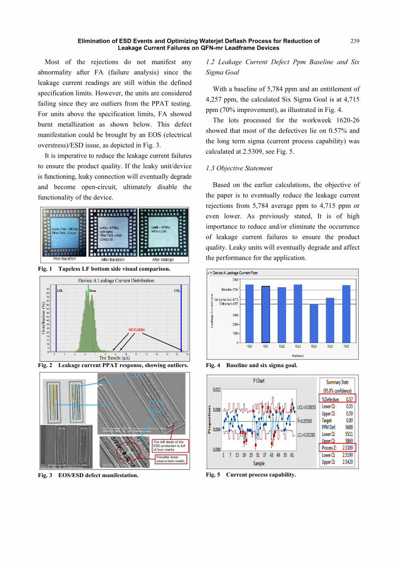
Most of the rejections do not manifest any
abnormality after FA (failure analysis) since the
leakage current readings are still within the defined
specification limits. However, the units are considered
failing since they are outliers from the PPAT testing.
For units above the specification limits, FA showed
burnt metallization as shown below. This defect
manifestation could be brought by an EOS (electrical
overstress)/ESD issue, as depicted in Fig. 3.
It is imperative to reduce the leakage current failures
to ensure the product quality. If the leaky unit/device
is functioning, leaky connection will eventually degrade
and become open-circuit, ultimately disable the
functionality of the device.
Fig. 1 Tapeless LF bottom side visual comparison.
Fig. 2 Leakage current PPAT response, showing outliers.
Fig. 3 EOS/ESD defect manifestation.
1.2 Leakage Current Defect Ppm Baseline and Six
Sigma Goal
With a baseline of 5,784 ppm and an entitlement of
4,257 ppm, the calculated Six Sigma Goal is at 4,715
ppm (70% improvement), as illustrated in Fig. 4.
The lots processed for the workweek 1620-26
showed that most of the defectives lie on 0.57% and
the long term sigma (current process capability) was
calculated at 2.5309, see Fig. 5.
1.3 Objective Statement
Based on the earlier calculations, the objective of
the paper is to eventually reduce the leakage current
rejections from 5,784 average ppm to 4,715 ppm or
even lower. As previously stated, It is of high
importance to reduce and/or eliminate the occurrence
of leakage current failures to ensure the product
quality. Leaky units will eventually degrade and affect
the performance for the application.
Fig. 4 Baseline and six sigma goal.
Fig. 5 Current process capability.

Elimination of ESD Events and Optimizing Waterjet Deflash Process for Reduction of Leakage Current Failures on QFN-mr Leadframe Devices
240
2. Review of Related Literature
Based on literature studies, some possible causes of
high leakage current rejections and damage or burnt
metallization related to assembly manufacturing
include electrostatic damage to sensitive devices,
tribocharging effects due to high waterjet parameters,
and high water resistivity during high-pressure
cleaning. ESD damage to units can be explained by
three models [1] as shown in Fig. 6.
The effect of high tribocharging brought by waterjet
deflash was also studied by Llana et al. [2]. Lower
waterjet pressure and temperature resulted to lower
supply current failures. Some of the failures were also
recovered after subjecting the units to baking or
removal of package moisture content.
Wafer saw process can also contribute to the unit’s
susceptibility to ESD damage, see Fig. 7. Processing
without CO2 bubbler or injector and ionizer showed
higher discharge voltage at 18.6 kV as compared to a
wafer saw process with the installed equipment [3].
Another study [4] showed that plasma process with
high cleaning parameters resulted to damage gate
oxide, as illustrated in Fig. 8.
At mold station, leakage current was also
experienced on some molding compounds due to
thermally induced/trapped charge failure mechanism
[5]. Some molding compounds also tend to have
carbon agglomeration, forming a conductive path thus
shorting adjacent pins [6].
3. Methodology
An ESD event mapping was carried out to
determine the scope of the ESD event measurement
and assessment. All process steps and equipment were
investigated since all of these steps could induce ESD
damage to the units (possible failure mechanism).
A handheld ESD event meter in Fig. 9 was used in all
process stations to measure any ESD event with
voltage setting at > 1 kV. Some limitations on the
measurement were encountered during curing process,
molding, and the waterjet deflash process. The
equipment at these processes could not be opened
while in active/working mode, hence limiting the
placement or location of the ESD event meter during
measurement.
Fig. 6 ESD models [1].
Fig. 7 Discharge voltage at wafer saw [3].
Fig. 8 Damage gate oxide with plasma process.
Fig. 9 Handheld ESD event meter by 3M™.

Elimination of ESD Events and Optimizing Waterjet Deflash Process for Reduction of Leakage Current Failures on QFN-mr Leadframe Devices
241
4. Results and Analysis
Assessment on the ESD event mapping is shown in
Table 1. Investigation showed that there were ESD
events on Diebonder A, causing higher leakage
current occurrence.
The equipment was then subjected to health check
and the ESD events were zeroed out by grounding the
machine floating parts. The assessment and the
corrective actions were considered quick wins,
causing the leakage current occurrence significantly
reduced from 5,784 ppm average to 1,567 ppm
average for workweek 1627-29.
After implementation of the corrective and
improvement actions, leakage current occurrence
greatly reduced from a baseline of 5,784 ppm to
average of 1,567 ppm last workweek 1627-29,
see Fig. 10. This is significantly better than the target
performance at 4,715 ppm.
4.1 Tribocharging Effects
As earlier mentioned, tribocharging is a source of
ESD. Factors like high rubbing speed, higher pressure,
lower relative humidity, and higher temperature
usually result in higher charge build-up. Shown in
Table 2 is the evaluation on possible tribocharging
effects in the assembly process.
Waterjet process with varying DI water resistivity
levels (high – 17 MΩ, low – 0.3 MΩ) shows
significant result, with p-value < 0.05 (p-value = 0 to
be exact, see Fig. 11), thus considered critical. This
zero leakage current PPAT was obtained for waterjet
deflash process with installed CO2 bubbler.
An illustration for tribocharging at waterjet station
and the setup for CO2 bubbler are shown in Fig. 12
and Fig. 13, respectively.
The CO2 bubbler has a resistivity setting ranging from
0.2 MΩ to 0.4 MΩ. This range value is still within the
static dissipative range. A static dissipative material
allows slow dissipation or attenuation of charge from
a charged device. The rate of discharge is slow and
controlled such that no damage is done to an ESD
sensitive device. The equivalent model representation
is shown in Fig. 14. With the addition of CO2 bubbler
to lower the resistivity (and resistance) of DI water,
the equivalent resistance of the discharge path
becomes Req = RDI // RCO2.
With lower Req, but still within the static
dissipative range, higher current I could flow to the
Table 1 ESD event mapping assessment.
Assembly process station
Section No. of ESD events (at > 1 kV)
Wafer Mount
Input 0
Mounter 0
Output 0
Wafer Saw Cutting 0
Spinner 0
Diebonder A Pick and place 12
Diebonder B Pick and place 0
Oven Cure Oven cure (standby mode) 0
Wirebonders Wirebond 0
Molding
Input 0
Chase (standby) 0
Output 0
Post Mold Cure Oven cure (standby mode) 0
Backetch Oven cure (standby mode) 0
Output 0
Waterjet DeflashInput 0
Output 0
Lasermark
Input 0
Marking 0
Output 0
Package Singulation
Input 0
Cutting 0
Pick and place 0
Fig. 10 Leakage current ppm improvement.

Elimination of ESD Events and Optimizing Waterjet Deflash Process for Reduction of Leakage Current Failures on QFN-mr Leadframe Devices
242
Table 2 Evaluation on tribocharging effects.
Y Unit of measure
Y treated as
X True nature of X
Levels of X p-value Decision Potential failure mechanism
Leakage Current
ppm
Discrete Wafer saw transfer arm speed
Discrete Low, high 0.282 X is not significant
ESD Damage
Discrete Wafer saw atomizing pressure
Discrete Low, high 0.058 X is not significant
Discrete Wirebond machine 1 ionizer
Discrete Good, defective
0.298 X is not significant
Discrete Waterjet water resistivity
Discrete Low, high 0 X is significant, hence, moves forward
Fig. 11 Proportion test on water resistivity levels.
Fig. 12 Tribocharging at waterjet deflash process.
Fig. 13 Installed CO2 bubbler at waterjet deflash process.
ground. Hence more amount of charge Q of the device
could be discharged at a period of time t.
To lower the water equivalent resistivity at waterjet
station, there are 2 possible options—use CO2 bubbler
or use RO (reverse osmosis) water with 0.1 MΩ
resistivity. Using the scoring matrix (higher score the
better), the use of CO2 bubbler is found to be more
cost effective and has lower risk of failure, refer to
Table 3. The use of RO water is more costly as there
is a need to invest on new facilities. Also, there is a
risk of foreign material deposition on the device if the
water is not deionized.
Pokayoke mechanism was installed so as not to
allow the waterjet machine to proceed when the water
resistivity is above the limit, brought by depleted CO2
tank or defective bubbler.
After optimization of the waterjet deflash process
and implementation of all corrective and improvement
actions, leakage current occurrence greatly reduced
from a baseline of 5,784 ppm to just 20 ppm for
workweek 1632-44, as highlighted in Fig. 15.
Fig. 14 ESD model, equivalent resistance of discharge path.
Table 3 Scoring matrix for lowering DI water’s resistivity.
Alternative SolutionSelection criteria*
Score Effectiveness Cost Quality
Use of CO2 Bubbler 9 9 9 729
Use of RO Water 9 7 7 441
* 9—high; 7—moderate; 3—low.

Elimination of ESD Events and Optimizing Waterjet Deflash Process for Reduction of Leakage Current Failures on QFN-mr Leadframe Devices
243
Fig. 15 Leakage current ppm improvement after optimization and implementation of all improvement and corrective actions.
Specifications such as FMEA (failure mode and
effects analysis), control plan, and work instructions
were updated based on the findings and the corrective
and improvement actions done.
5. Conclusion
Leakage current failures were significantly reduced
from 5,784 ppm average to 20 ppm for workweek
1632-44 by optimizing the waterjet deflash process by
reducing the water resistivity through the use of CO2
bubbler, eliminating ESD events through grounding of
floating machine parts, ensuring the allowed
resistance value according to the specifications, and
sustaining ESD controls. This great achievement took
into account and in mind the motivation to deliver
high quality products to customers given the
fast-paced and demanding market.
Acknowledgments
The authors would like to extend the appreciation
and credits to all members of the leakage current task
force team and to the STMicroelectronics Calamba
Management Team.
References
[1] ESD Association, Fundamentals of ESD, Device Sensitivity and Testing, Rome, NY, 2011.
[2] Llana, F., et al., 2016. “Practical, Cost Efficient, and Systematic Approach in Resolving Supply Current Failures during Unit Testing of QFN-mR BiCMOS Device.” Presented at 26th ASEMEP Technical Symposium.
[3] Disco Engineering and R&D Division. 2016. “Wafer ESD in Dicing Saws and the Effect of the Countermeasures.” Dicer Engineering Department, Disco.
[4] Padilla, E., et al. 2015. “Plasma Optimization in Addressing Test Leakage Fails for BCD Wafer Technology.” Presented at the 25th ASEMEP Technical Symposium.
[5] Mosbarger, R., and Hickey, D. J. 1994. “The Effects of Materials and Post-Mold Profiles on Plastic Encapsulated Circuits.” In Proceedings of Reliability Physics Symposium, 1994, 32nd Annual Proceedings, San Jose, CA, USA.
[6] Singh, A. 2017. “Investigation and Resolution of Current Leakage Failure Caused by Carbon Black Agglomeration in Mold Compound.” International Symposium on Microelectronics 2017 (1): 000685-8.