elex -experiment 5
DESCRIPTION
experimentTRANSCRIPT

I. OBJECTIVES
1. To determine quiescent voltages and currents of a voltage divider circuit.
2. To construct DC loadline from the saturated current and cut-off voltage.
3. To investigate the biasing accuracy of a voltage divider circuit
II. BASIC CONCEPT
The voltage divider bias circuit is by far the most commonly used. It has the stability of an emitter bias circuit, yet does not require a dual polarity power supply for its operation. The voltage divider bias circuit uses a simple voltage divider to set the value of VB. It is made up of R1 and R2 // Rin(base). If R1 is much larger than IB (IR1 > 10xIB) we can assume that VB = VR2 thus, VB is found in this amplifier as
VB = R2 VCC / R1 + R2
The emitter voltage is then found as
VE = VB – 0.7V
Once the emitter voltage has been determined, Ohm’s Law can be used to find the value of IE, as follow:
IE = VE/RE
Now, assuming that ICQ = IE, VCEQ can be found as
Vceq = VCC – IE (RC + RE)
Biasing is the application of dc voltage in order for the transistor to function properly. With proper biasing, ac signals can be applied to the transistor input resulting in amplified non-distorted output signal. The biasing circuit determines the dc operating point for the transistor. The bias circuit is composed of the dc power sources, the transistor and resistors. The dc voltages and currents in the circuit establish the dc operating point. The dc operating point is also known as the quiescent point or Q-point. The Q-point establishes the dc voltages and currents which amplification will take place for the transistor.
III. MATERIALS
EXPERIMENT 5: VOLTAGE DIVIDER BIASING
Quantity Description1 50KΩ (1/2 W)1 10KΩ (1/2 W)1 1KΩ (1/2 W)1 5KΩ (1/2 W)2 2N3904 NPN transistor1 0 – 15V DC Power Supply1 VOM1 Breadboard1 set of connecting wires
IV. WIRING DIAGRAMS
Q12N3904
R150kΩ
R210kΩ
RC5kΩ
RE1kΩ
V1
15 V
1
2
3
4
0
Figure 5.1 Voltage Divider Biasing Circuit
V. PROCEDURE
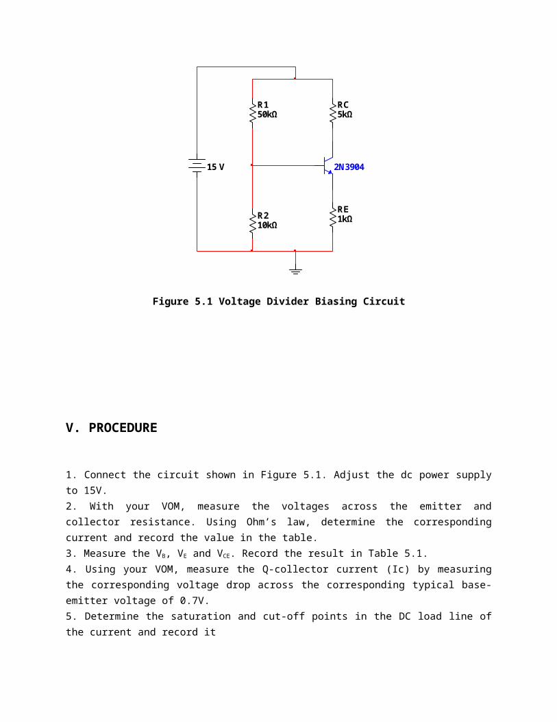
1. Connect the circuit shown in Figure 5.1. Adjust the dc power supply to 15V.2. With your VOM, measure the voltages across the emitter and collector resistance. Using Ohm’s law, determine the corresponding current and record the value in the table.3. Measure the VB, VE and VCE. Record the result in Table 5.1.4. Using your VOM, measure the Q-collector current (Ic) by measuring the corresponding voltage drop across the corresponding typical base-emitter voltage of 0.7V.5. Determine the saturation and cut-off points in the DC load line of the current and record it
VI. DATA AND RESULTS
Table 5.1PARAMETER MEASURED VALUE EXPECTED VALUE % ERROR
VB 2.404VC 6.432VE 1.725VCE 4.707VRC 8.568ICSAT
VCECUT-OFF
VII. SAMPLE COMPUTATIONS

VIII. GRAPHS
IX. ANALYSIS OF RESULTS
X. CONCLUSIONS

XI. SELF-TEST QUESTIONS
1. Voltage divider bias is noted for itsa. varying emitter currentb. unstable voltage at collectorc. stable quiescent point (Q-point)d. very large base current
2. What are the advantages of voltage divider over the base bias and the emitter bias?

XII. APPLICATION (CIRCUIT SIMULATION)
Based on the readings appearing in the Figure, determine whether the transistor is “ON” and the network is operating properly by simulating the circuit and proving the result by computation.
Q1
2N1711
R1
4.7kΩ
R21kΩ
R3
20kΩ
R4
80kΩ
20V
3.3V
20V