electronic system modelling of ut pulser-receiver and...
TRANSCRIPT

BRUNEL UNIVERSITY
Electronic System Modelling of UT Pulser-Receiver and the
Electron Beam Welding Power Source
By
Thayaparan Parthipan
A thesis submitted in partial fulfilment for the degree of Engineering Doctorate
In the
School of Engineering and Design
September 2013

i
ABSTRACT
Continuous improvements to industrial equipment used in essential industrial
applications are a key for the commercial success to the equipment manufacturers. Industrial
applications always demand optimum performance and reliability and almost all equipment used
in industrial applications is complex and are very expensive to replace. Often modifications to
hardware and retrofitting additional hardware are encouraged by most equipment manufacturers
and operators. The complexity of these systems however, makes assessment of modifications and
design change difficult. This research implemented system modelling techniques to overcome
this issue, by developing virtual test platforms of two distinctive industrial systems for
enhancement assessment. The two distinctive systems were the electronic equipment called
pulser-receiver used in ultrasonic non-destructive testing of safety critical oil & gas pipelines and
a high voltage power supply used in high energy electron beam welding. Optimisation with
emphasis on portability of the pulser-receiver and rapid weld recovery after a flashover fault
condition in the electron beam welding application required assessment before design changes
were made to hardware. SPICE based simulators LTSpice and PSpice were used to model and
simulate the pulser-receiver and the welding power supply respectively. All the models were
evaluated appropriately against theoretical data and published datasheets. However, validation of
low level component models developed in the research against measurement data at a component
level suffered due to system complexity and resource constraints. Close mapping of simulation
results to measurement data at a system level were obtained. The research helped build up a
wealth of knowledge in the development of circuit simulation models that can be analysed in the
time domain with no non-convergent issues. Simulation settings were relaxed without
compromising accuracy of model performance.

ii
ACKNOWLEDGEMENTS
The author extends his eternal gratitude to all those who have helped in the project, at
Brunel University, the University of Surrey and TWI ltd. The work could not have been
completed without the help and support of the project supervisors Dr. Rajagopal Nilavalan,
Professor Wamadeva Balachandran, Colin Ribton and Professor Peter Mudge, as well as that
from Dr. Mohamed Darwish, Barry Elborn and many other colleagues too numerous to mention
here. The continued camaraderie from other Research Engineers on the Brunel/Surrey EngD
Programme, both past and present, has also been an essential ingredient and is very gratefully
acknowledged, as is the permanent support and encouragement from family and friends.
Special thanks go to Dinesh Chamund at Dynex Semiconductor, Peter Johns from
International Transformers and Mark Mayes from Linear Technology (Arrow Electronics) for all
the materials they provided towards the research. For the project funding, thanks and recognition
must also be apportioned to The Engineering and Physical Sciences Research Board (EPSRC)
and TWI Ltd., without whom the research would not have been possible.
I also would like to thank my wife, Kavita for her constant support and encouragement, my son
Kathiravan for proof reading some of my work and my daughter Kartikaa for helping me to keep
things in prospective.

To my mother, father, uncles and aunts

iii
CONTENTS
Abstract ................................................................................................................................ i
Acknowledgements ............................................................................................................. ii
Contents ............................................................................................................................. iii
List of figures ...................................................................................................................... x
List of tables ..................................................................................................................... xvi
Abbreviations ................................................................................................................. xviii
List of symbols .................................................................................................................. xx
1 Introduction .................................................................................................................. 1
1.1 Introduction ........................................................................................................... 1
1.2 Long Range Ultrasonic Testing technique ............................................................ 3
1.3 Electron Beam Welding application ..................................................................... 3
1.4 Motivation ............................................................................................................. 4
1.4.1 Pulser-receiver optimisation for portability .................................................... 5
1.4.2 Electron beam welding power supply enhancement for void-free welding .... 5
1.5 Scope of the thesis ................................................................................................. 6
1.6 Circuit simulation using SPICE based program .................................................... 7
1.6.1 Simulation tool selection ................................................................................. 8

Contents
iv
1.6.2 Simulation models ......................................................................................... 11
1.6.3 Transient analysis .......................................................................................... 12
1.6.4 Convergence issues ....................................................................................... 13
1.6.5 System modelling methodology .................................................................... 14
1.6.6 Meeting simulation software requirement..................................................... 15
1.7 Contribution to knowledge .................................................................................. 17
1.8 Structure of the thesis .......................................................................................... 19
1.9 Publications ......................................................................................................... 20
2 Long Range Ultrasonic Testing .................................................................................. 22
2.1 Overview ............................................................................................................. 22
2.2 LRUT technique .................................................................................................. 22
2.3 Plant Integrity’s LRUT system ........................................................................... 23
2.4 Applications ........................................................................................................ 24
2.5 Application specific issue – portability ............................................................... 25
2.6 Limitations .......................................................................................................... 27
2.7 Research methodology ........................................................................................ 28
2.8 LRUT system architecture .................................................................................. 28
2.8.1 Functionality.................................................................................................. 30
2.8.2 Load ............................................................................................................... 32
2.8.3 Pulser-receiver unit ....................................................................................... 34

Contents
v
2.8.4 Digital hardware ............................................................................................ 34
2.8.5 Data converters .............................................................................................. 36
2.8.6 Transmit circuit ............................................................................................. 37
2.8.7 Receive circuit ............................................................................................... 38
2.8.8 Power supplies............................................................................................... 39
2.8.9 Primary power source – the battery............................................................... 40
2.9 Identification of crucial components ................................................................... 41
2.10 Variant of application ...................................................................................... 45
2.10.1 Medium frequency application.................................................................... 46
2.11 Summary .......................................................................................................... 46
3 Enhancement of Pulser-Receiver for Long Range Ultrasonic System ....................... 48
3.1 Overview ............................................................................................................. 48
3.2 Modelling of an Electro-Mechanical Load ......................................................... 48
3.2.1 Modelling of an EBL#2 piezoelectric transducer ......................................... 51
3.2.2 Modelling of LRUT transducer ..................................................................... 55
3.2.3 Transducer array ............................................................................................ 57
3.3 Modelling of pulser-receiver unit ........................................................................ 59
3.3.1 Transmit Circuit ............................................................................................ 60
3.3.2 Power Budget Analysis with transducer array .............................................. 65
3.3.3 Receive Circuit .............................................................................................. 68

Contents
vi
3.3.4 Power estimation of Digital logic and Data Converters ................................ 72
3.4 Power Supplies .................................................................................................... 76
3.4.1 High Voltage Power Supply .......................................................................... 77
3.5 Power budgeting and battery modelling.............................................................. 91
3.6 Hardware realisation ........................................................................................... 99
3.6.1 PSU prototype ............................................................................................. 100
3.7 Summary ........................................................................................................... 102
4 Medium frequency LRUT application – System Model reuse ................................. 107
4.1 Overview ........................................................................................................... 107
4.2 Medium frequency LRUT application .............................................................. 107
4.3 Reusability of existing hardware ....................................................................... 108
4.4 Development of high frequency transmit circuits ............................................. 109
4.4.1 Transducer model and its performance ....................................................... 110
4.4.2 Medium frequency transmit circuit ............................................................. 111
4.4.3 Medium frequency receive circuit............................................................... 114
4.4.4 Power supplies............................................................................................. 115
4.4.5 Typical system level simulation .................................................................. 116
4.5 Hardware implementation and system integration ............................................ 119
4.6 Summary ........................................................................................................... 121
5 Electron beam welding system ................................................................................. 123

Contents
vii
5.1 Overview ........................................................................................................... 123
5.2 Electron beam welding process ......................................................................... 123
5.2.1 Electron beam Generation ........................................................................... 124
5.2.2 High power requirement.............................................................................. 125
5.3 Description of the EBW System components ................................................... 127
5.3.1 High voltage DC power supply ................................................................... 128
5.3.2 Vacuum chamber......................................................................................... 129
5.3.3 CNC and auxiliaries .................................................................................... 129
5.3.4 Micro-discharge, flashover and prevention ................................................. 130
5.3.5 System recovery after flashover .................................................................. 133
5.4 Summary on findings ........................................................................................ 134
5.5 Introduction to the EBW power source ............................................................. 136
5.5.1 Power conversion stages ............................................................................. 136
5.5.2 Power semiconductor device technology .................................................... 141
5.5.3 Control electronics ...................................................................................... 143
5.6 System enhancement constraints ....................................................................... 143
5.7 Identification of critical components................................................................. 144
5.8 Conclusion ......................................................................................................... 145
6 Modelling of electron beam welding power source ................................................. 146
6.1 Overview ........................................................................................................... 146

Contents
viii
6.2 Modelling of the H – Bridge inverter ................................................................ 146
6.2.1 Effect of parasitic elements ......................................................................... 149
6.2.2 Modelling of IGBT and FWD ..................................................................... 151
6.2.3 IGBT and FWD model evaluation .............................................................. 153
6.3 Control electronics modelling ........................................................................... 162
6.3.1 Output power characterisation and system stability .................................... 163
6.3.2 Fault detection and recovery ....................................................................... 172
6.4 Transformer modelling and inclusion of the saturation effect .......................... 174
6.5 Load behaviour and modelling .......................................................................... 177
6.6 Top level simulation and analysis ..................................................................... 179
6.6.1 Output ripple analysis.................................................................................. 185
6.6.2 Fault detection and recovery ....................................................................... 188
6.6.3 Evaluation of system level operation .......................................................... 190
6.7 Applications ...................................................................................................... 193
6.7.1 System stability ........................................................................................... 193
6.7.2 System modelling fault recovery control circuit enhancement ................... 194
6.8 Summary ........................................................................................................... 197
7 Conclusions and recommendations for further work ............................................... 198
7.1 Discussion on LRUT pulser receiver model ..................................................... 200
7.2 Functional analysis of EBW power source ....................................................... 202

Contents
ix
References ....................................................................................................................... 205
Appendix A: Modelling of electromechanical components in SPICE ................................ I
A 1. Lossy transmission line model ........................................................................... I
A 2. Electromechanical model description ................................................................ II
A 3. Model development of EBL#2 piezoelectric transducer element ................... IV
A 4. Modelling of backing mass........................................................................... VIII
A 5. Modelling of face plate .................................................................................... IX
A 6. Medium – the test specimen ............................................................................ IX
A 7. Integration of models ........................................................................................ X
Appendix B: Electron beam welding power source models ................................................ I
B 1. Power stage – The H-Bridge inverter ................................................................ II
B 2. Power stage - High voltage transformer and the EBW-Gun ........................... IV
B 3. IGBT drive circuits ....................................................................................... VIII
B 4. Control circuits ................................................................................................. X

x
LIST OF FIGURES
Figure 2-1 Example LRUT system and its components – PI Ltd.’s system ................................. 23
Figure 2-2 LRUT of offshore risers and remote pipelines using a pulser-receiver unit ............... 25
Figure 2-3 MK3 Pulser-receiver unit and its internal view .......................................................... 26
Figure 2-4 Simplified architecture of LRUT system .................................................................... 29
Figure 2-5 A-Scan showing category level guide superimposed on captured data ...................... 31
Figure 3-1 Shear mode (1-5) operation of a piezoelectric transducer .......................................... 49
Figure 3-2 EBL#2 Piezoelectric transducer impedance characteristics and sample specific
parameters (EBL Piezoelectric precision 2010) ....................................................... 50
Figure 3-3 Equivalent circuit model evaluation for EBL#2 piezoelectric transducer .................. 54
Figure 3-4 LRUT-Transducer impedance characteristics for the application range..................... 56
Figure 3-5 LRUT-Transducer production test results (Neal 2010) .............................................. 57
Figure 3-6 Impedance analysis of array size; 13 LRUT-transducers ........................................... 58
Figure 3-7 Simplified architecture of the pulser-receiver unit showing its main components ..... 59
Figure 3-8 Simplified diagram of a transmit circuit ..................................................................... 62
Figure 3-9 The graph shows all major power consuming components in the transmit circuit
together with the power budget values .................................................................... 65
Figure 3-10 Transmit circuit power consumption revealed .......................................................... 65
Figure 3-11 Receive circuit implemented in the pulser-receiver unit ........................................... 68
Figure 3-12 Bode plot showing functionality of receive circuit ................................................... 69
Figure 3-13 Receive circuit power performance .......................................................................... 70
Figure 3-14 Transient simulation depicting the clipping of the receive circuit output ................. 71

List of figures
xi
Figure 3-15 FPGA dynamic power consumption ......................................................................... 74
Figure 3-16 Pulse load application of pulse-receiver unit ............................................................ 78
Figure 3-17 Simulation model of CCPS ....................................................................................... 81
Figure 3-18 Operation of HTPSU (a. Simulation; b: Measurement). The charging current Ipri
sourced from the battery (a: Id(Q1); b: CH1), switching signal (a: Vn013; b: CH2) and
the charge voltages ( a: Vout+, Vout-; b: CH3, 4) are shown ...................................... 84
Figure 3-19 FFT of the switching signal (a: simulation; b: measurement) and guidance data from
(LT3751 2008) ......................................................................................................... 85
Figure 3-20 Boundary mode operation (BM) of the HTPSU (a: Simulation; b: Measurement).
Voltage across the switching device VDS (a: VVDS; b: CH4) is as high as 65V due to
Lleakage. BM of the HTPSU is noticeable as the drain current (a: Id(Q1); b: CH1) dies
with the switching off of Q1 (a: Vgate; b: CH2) ........................................................ 87
Figure 3-21 The average drain current (Id) passing through the switching device Q1 as the
charging cycle is closer to the completion (simulation data). .................................. 88
Figure 3-22 Loading of HTPSU with 1.8 A load current when Vout+ and Vout- are charged to
±150V (top: square pulse; bottom: tone burst) in simulation. With a tone burst a
voltage drop of 3V was experienced ........................................................................ 89
Figure 3-23 Sequence of battery current in one LRUT cycle ....................................................... 92
Figure 3-24 Equivalent circuit model of the battery pack resembling the prototyped battery pack.
Each cell is an exact model of (Gold 1997) and parameterised to match Teletest
battery pack. Load is provided by a current source. ................................................ 95
Figure 3-25 Imitated discharge current loading the battery pack simulation model .................... 96
Figure 3-26 Real hardware loading effect on the Li-Ion battery simulation model ..................... 98

List of figures
xii
Figure 3-27 Number of completed LRUT cycles in simulation ................................................... 98
Figure 3-28 Number of completed LRUT cycles and battery terminal voltage drop ................... 99
Figure 3-29 Power electronics hardware for pulser-receiver unit .............................................. 100
Figure 3-30 HT-Bank together with its associated transmit and receive circuit......................... 101
Figure 3-31 Pulser-receiver unit as a commercial product ......................................................... 102
Figure 4-1 Complex structure of an aircraft wing assembly component (Haig & Stavrou 2012)
................................................................................................................................ 108
Figure 4-2 Medium frequency LRUT hardware architecture ..................................................... 109
Figure 4-3 Impedance characteristics of an LRUT transducer for extended 1 MHz application 111
Figure 4-4 Bode plot of the medium frequency transmit circuit in simulation .......................... 113
Figure 4-5 Excitation signal driving LRUT-Transducer showing 190Vpk-pk; at 1 MHz (a:
simulation; b: measurement) .................................................................................. 114
Figure 4-6 Bode magnitude plot, showing receive circuit’s performance in simulation ............ 115
Figure 4-7 Multi-engineering domain system simulation of the medium frequency circuits ..... 117
Figure 4-8 Medium frequency system simulation for excitation frequencies a: 1 MHz and b: 500
kHz ......................................................................................................................... 118
Figure 4-9 Experimental setup for high frequency LRUT on sample while developing a crack 119
Figure 4-10 LRUT excitation at 500 kHz with crack size 0 mm (a) and 5 mm (b) .................... 120
Figure 5-1 Weld penetration vs. electron beam power applied (reproduced from (Hanson 1986))
................................................................................................................................ 126
Figure 5-2 Simplified EBW system ............................................................................................ 127
Figure 5-3 Weld defect caused by major discharge (Sanderson 1986) ...................................... 131
Figure 5-4 Block diagram of the high voltage power supply ..................................................... 137

List of figures
xiii
Figure 5-5 Simplified schematic diagram of the SMPS used in the EBW system ..................... 137
Figure 5-6 Large system makes access restriction ...................................................................... 144
Figure 6-1 Simplified diagram of H-Bridge inverter .................................................................. 147
Figure 6-2 Diode commutation in inverter operation ................................................................. 148
Figure 6-3 IGBT output characteristics comparison ................................................................... 154
Figure 6-4 Simulation circuits for gate charge transient and switching characteristics (right) .. 157
Figure 6-5 Simulation results showing switching characteristics ............................................... 159
Figure 6-6 Free wheel diode forward and reverse recovery current characteristics ................... 161
Figure 6-7 Voltage-mode feedback control of the SMPS for voltage output - VKVOUT stability 163
Figure 6-8 PWM signal generation ............................................................................................. 164
Figure 6-9 PWM controller UC3825/ SG1825 architecture and its main components .............. 166
Figure 6-10 Open loop Bode plot of the SG1825 error amplifier PSpice model ....................... 169
Figure 6-11 Pole-Zero diagram of the system ............................................................................ 171
Figure 6-12 High voltage transformer core dimensions ............................................................. 176
Figure 6-13 B-H curve of the High voltage transformer core .................................................... 177
Figure 6-14 The I-V characteristics of an electron beam welding gun....................................... 178
Figure 6-15 Top level stitching of subsystems ........................................................................... 181
Figure 6-16 EBW Power source top level simulation model functionality ................................ 182
Figure 6-17 Simulation showing a typical flashover free 150 kV; 600 mA power delivery ...... 183
Figure 6-18 Inverter current for light and heavy load ................................................................. 184
Figure 6-19 Acceleration voltage VKVOUT ripple explained (Note: Not drawn to scale) ............ 185
Figure 6-20 Conversion of inverter output current into DC for overcurrent detection (simulation)
................................................................................................................................ 189

List of figures
xiv
Figure 6-21 Simulation showing flashover detection and VKVOUT recovery in 30 ms ............... 190
Figure 6-22 Inverter performance: figures a and c show the measurement on real inverter
hardware depicting inverter output +/-610V and one of the IGBTs switching 300A
and 600 A respectively. Figures b and d shows the corresponding waveforms in
simulation for 300 A an 600 A respectively. ......................................................... 191
Figure 6-23 Stability of the system ............................................................................................. 193
Figure 6-24 Fault recovery time optimisation ............................................................................ 196
Figure A- 1 Schematic of the LRUT transducer and the test specimen .......................................... II
Figure A- 2 An equivalent circuit model developed in LTSpice .................................................. III
Figure A- 3 Puttmer model (Scott & Philip 2008) ........................................................................ IV
Figure B- 1 H-Bridge inverter model based on IGBT DIM800DDM12-A000 model ................... II
Figure B- 2 PSpice model for DIM800DDM12-A000 ................................................................. III
Figure B- 3 PSpice model for the free wheel diode of DIM800DDM12-A000 ........................... IV
Figure B- 4 Models of high voltage transformer arrangement and load........................................ V
Figure B- 5 High voltage rectifier diode arrangement .................................................................. VI
Figure B- 6 EBW Gun model ...................................................................................................... VII
Figure B- 7 IGBT drive circuits ................................................................................................. VIII
Figure B- 8 IGBT driver circuit functionality of driving IGBTs Z3 and Z4 ................................. X
Figure B- 9 Control circuit model: PWM circuits ........................................................................ XI
Figure B- 10 Control circuit model: a kV demand circuit ........................................................... XII
Figure B- 11 Weld dead time ..................................................................................................... XIII

List of figures
xv
Figure B- 12 Simulation showing 23 ms dead time and 7 ms ramp time .................................. XIV
Figure B- 13 Control circuit model: kV actual circuit ................................................................. XV
Figure B- 14 Control circuit model: Inverter current measurement circuit ............................... XVI
Figure B- 15 Fault detection circuit model: Flashover detection ............................................ XVIII
Figure B- 16 Fault detection circuit: Dead time set circuit ........................................................ XIX

xvi
LIST OF TABLES
Table 2-1 Topologies used to construct the pulser-receiver unit power supplies ......................... 40
Table 3-1 EBL#2 piezoelectric transducer extracted parameters from manufacturer’s data ........ 51
Table 3-2 Transmit circuit specification ....................................................................................... 61
Table 3-3 Transmit circuit calculations ........................................................................................ 61
Table 3-4 Transmit circuit power consumption summary; ideal capacitor vs. load model .......... 67
Table 3-5 FPGA static power estimation ...................................................................................... 73
Table 3-6 Power budgeting of data converters ............................................................................. 76
Table 3-7 High voltage power supply specification ..................................................................... 80
Table 3-8 High voltage power supply functional parameter calculation ...................................... 82
Table 3-9 Flyback High voltage power supply efficiency ............................................................ 90
Table 3-10 function description .................................................................................................... 93
Table 3-11 Power budgeting table ................................................................................................ 94
Table 4-1 Medium frequency transmit circuit specification ....................................................... 111
Table 4-2 Medium frequency transmit circuit calculations ........................................................ 112
Table 6-1 IGBT switching transient Device parameters defined (Mitsubishi Electric 1998) .... 159
Table 6-2 PWM triangular ramp signal profile........................................................................... 168
Table 6-3 Transformer core parameters ...................................................................................... 176
Table 6-4 Output voltage ripple calculation ............................................................................... 187
Table A- 1 EBL#2 piezoelectric transducer data extracted from (EBL Piezoelectric precision
2010) and measurement ........................................................................................... VI

List of tables
xvii
Table A- 2 Calculation of piezoelectric material properties of the EBL#2 transducer ............... VII
Table A- 3 Model parameters for developing Puttmer model for EBL#2 transducer ................. VII
Table A- 4 Material properties used to calculate acoustic impedance of the Steel backing mass
............................................................................................................................... VIII
Table A- 5 Face plate model parameters calculation, using Al2O3 material properties ............... IX
Table A- 6 Material properties of the medium and its calculated model specific values .............. X
Table B- 1 Model parameters for DIM800DDM12-A000 PSpice model .................................... IV
Table B- 2 HV Transformer core parameters included in the Jiles-Atherton model .................... VI
Table B- 3 Ramp time setup ........................................................................................................ XV
Table B- 4 Current limit threshold values................................................................................. XVII

xviii
ABBREVIATIONS
ABM
Analogue Behavioural Models
AC
Alternating Current
ADC
Analogue to Digital Converter
CMOS
Complementary metal-oxide-semiconductor
DAC
Digital to Analogue Converter
DC
Direct Current
DDR2
Double Date Rate synchronous memory
DSN
Distributed Sensor Network
EBA
Electron Beam Acceleration
EBW
Electron Beam Welding
EDA
Electronic Design Automation
EMI
Electro Magnetic Interfurance
ENOB
Equivalent number of bits of an ADC
FEA
Finite Element Analysis
FPGA
Field Programmable Gate Array
FWD
Free Wheel Diodes
HT-Bank
Bulk capacitor bank used in the pulser receiver
HTPSU
High Volrage power supply used in pulser-receiver
IC
Integrated Circuits
IGBT
Insulated Gate Bipolar Transistor
I-V
Current-Voltage characteristics

Abbreviations
xix
LASER
Light Amplified by Stimulated Emission of Radiation
LRUT
Long Range Ultrasonic Testing
NDT
Non-Destructive Testing
nMOS
n-channel MOSFET transistor
NPT IGBT
Non-Punch-Through IGBT
NVEBW
Non Vacuum Electron Beam Welding
PC
Personal Computer
PCB
Printed Circuit Board
PHY
Physical layer of the Ethernet controller device
PM
Phase margin
PRR
Pulse Repitition Rate
PSRR
Power Supply Rejection Ratio
PT IGBT
Punch-Through IGBT
PZT
Lead Zirconate Titanate piezoelectric transducer
SMPS
Switch Mode Power Supply
SPICE
Simulation Program with Integrated Circuit Emphasis
TWI
The TWI Ltd.
UT
Ultrasonic Non Destructive Testing
VHDL
Very high speed Hardware Description Language

xx
LIST OF SYMBOLS
A Area - m2
C55
Elastic stiffness constant - N/m2
CLOAD Capacitive load
CT
Free capacitance of an piezoelectric transducer measured at 1 kHz - F
d15 Piezoelectric charge constant - C/N
dB Decibel
e0 Permittivity of free space - C/Vm
E11S Piezoelectric stress constant under constant strain - C/N
E11T
Piezoelectric stress constant under constant stress - C/m2
fa / fp Antiresonance or Parallel resonance frequency - Hz
Fext Frequency of excitation signal used for transducer excitation - Hz
fr Resonance frequency - Hz
g15 Piezoelectric voltage stress constant - Vm/N
GPA Gain of power amplifier
Id Drain voltage of MOSFET - A
k15 Shear coupling factor
Qm Mechanical quality factor
S55D
Elastic compliance coefficient under constant electric displacement - m2/N
S55E
Electric compliance coefficient under constant electric field - m2/N
v Velocity of an electron - m/s
V5D
Sound velocity - m/s, 1

List of symbols
xxi
VCE Collector-Emitter voltage across
VKVOUT Acceleration voltage
Vp Sound velocity (also labeled as V5D) - m/s
Vr Relativistically-corrected acceleration voltage - V
Wb Power density - kW/cm2
XC Impedance of a capacitive load
π 3.141592654, 1
ρ Density - kg/m3

1
1 INTRODUCTION
1.1 Introduction
Better understanding of the operation and performance of systems and their constituent
components is crucial when it comes to adapting hardware changes or modifications. Such
changes are required mainly for performance enhancement of the overall system or at a
component level. Components may be a single device or may be a subsystem consisting of a
number of individual devices.
Performance of the constituent components and the interaction between them varies for
different functionalities and scenarios in most systems and this variation consequently affects the
overall performance of the system. These components’ functionality in general is electronic,
mechanical, chemical, or acoustic or a combination of more than one of these aspects; making
the component and hence the system a multi-engineering discipline. This increases the
complexity of system analysis and makes it an arduous and time consuming task to analyse and
optimise the systems in their entirety.
Modelling the systems and simulating the developed model in a computing environment
has been proven as a flexible means of achieving this aim efficiently. Validation and assessment
of systems and components by system modelling has been extensively published in the literature.
Some of the work sited in the literature relates to system modelling as follows: In avionics and
the space sector, being conservative in their design approach (as many failures have a safety
implication), the assessment of components is a must. A systematic approach of modelling and
simulating avionics hardware and software for assessing components at a subsystem level was

1 Introduction
2
discussed by (Bluff 1998), and examples such as analysis of aerospace circuit fault analysis by
(Signal & Somanchi 1998), performance analysis of improved power electronics for aircraft
ventilation and air-conditioning motors (Athalye 1999) at a component level and battery life
assessment of space probe by (Michael 1998) are evidence of the powerfulness of the system
modelling techniques. Likewise in automotive engineering, where reliability and cost are
paramount, system modelling has been used extensively to qualify automotive subsystems such
as works published by (Ryan & Philip 2008); estimating battery capacity for an electric vehicle,
(Donnelly & Gauen 1993); a high power switching device evaluation on an ignition system, and
(Metzner, Schafer & Chihao 2001); looking at modelling mixed-signal electronic components
used in an automotive application for performance analysis. Evidence of utilising system
modelling techniques for foreseeing uncertainties in a distributed sensor network (DSN), that
mostly fails prematurely due to a lack of power, has also been sighted in the literature (Wei
2007), (AboElFotoh, Iyengar & Chakrabarty 2005).
The Long Range Ultrasonic Testing (LRUT) pulser-receiver unit and the Electron Beam
Welding (EBW) power source are two distinctive industrial systems. The LRUT pulser-receiver
unit is used in ultrasonic Non-Destructive Testing (UT) applications for structural health
monitoring of operational sensitive components. The EBW power source is a high power Switch
Mode Power Supply (SMPS), which provides high power (100 kW) for precision EBW of high
value components. Reliable and optimal performances of these complex systems are critical for
the smooth operation of industrial applications, LRUT and EBW. The research focussed on
developing simulation models of these two distinctive industrial systems, which can be simulated
in a computer environment for performance analysis and subsequent modification to their
hardware for their enhanced performance.

1 Introduction
3
1.2 Long Range Ultrasonic Testing technique
Industry needs reliable cost effective technologies for continuous or scheduled structural
monitoring of structures. UT is a method of inspecting the condition of structures and
components using ultrasonic waves. This method ensures that the material and its mechanical
properties are not damaged or compromised. LRUT is a subset of UT that has the ability to
detect defects for many metres in different shapes and type of structures such as pipes
(Gharaibeh 2008), (Mudge, Lank & Alleyne 1994), rails (Gharaibeh et al. 2010) and plates
(Mudge & Catton 2006). This technique enables the inspection to be carried out from a single
point of access if required (Parthipan 2010).
The effectiveness of this technique has broadened its applications, from pipe inspection
to inspection of various complex and vast structures such as offshore wind-turbine towers and
offshore platforms. These structures mostly operate in remote, harsh environments. Compliance
with international standards, aimed at ensuring reliability and safety (e.g., ISO 19900 and ISO
19902) whilst operating in a harsh environment requires periodic condition monitoring of
structures. An electronic portable pulser-receiver unit facilitates application of the LRUT
technique on site. The unit uses ultrasonic waves to detect anomalies by sending ultrasonic
waves along the specimen and then processes the ultrasonic waves received. The received signal
can either be a reflection from the defects when operated in the pulse-echo method or the shadowed
image after the defects in the pitch-catch method.
1.3 Electron Beam Welding application
EBW is a welding process in which a high velocity electron beam is applied to the
materials being joined. The process melts the work piece by transforming the kinetic energy of the

1 Introduction
4
electron beam into heat upon impact. It is very popular in industrial applications such as
aerospace, marine, nuclear waste burial and automotive for its high integrity, low distortion,
higher welding speed, lower heat input, and greater depth-to-width aspect ratios than any of the
other fusion welding methods (Fritz et al. 1998), (Russell 1981), (Schulze & Powers 1998). A
high voltage potential (150 kV in typical applications) is required between the welding electrodes
(Electron beam gun anode and cathode) to gain high velocity. The required voltage level is achieved
using a transformer-rectifier fed with a single phase from a switch mode inverter unit, based on an H-
Bridge inverter.
1.4 Motivation
Electronic systems that are deployed on industrial applications in general incorporate
complex hardware. Their reliability and optimal performance is a key factor for their commercial
success. Typically these systems are a fabrication of a number of subsystems, whose function
differs from each other, but which are inter-dependent on each other. This makes fault
diagnostics for maintenance and implementing modifications for enhancement complicated.
Moreover, the application specific nature of their design and operation always requires expert
knowledge when it comes to repair, maintenance, enhancement and usage of this hardware. This
adds cost and intensive resource usage for the equipment developers, with a negative impact on
maintenance downtime and product development cycle time.
Electronic system hardware that facilitates the LRUT technique and EBW applications
are complex architectures. Consequently when examining the hardware for maintenance or
enhancement, or when making changes to the system for trials, there is a risk of the system being
damaged and/or equipment safety being compromised. However, continuous improvements to

1 Introduction
5
find and implement modifications for reliability, and update performance enhancement is
necessary for equipment manufacturers and service providers to maintain a lead. Therefore, a
reliable method to appropriately analyse these complex systems is required, so that maintenance
and product development can be carried out quickly, economically and safely.
1.4.1 Pulser-receiver optimisation for portability
A battery powered portable electronic equipment generally known as a pulser-receiver
(see section 2.3 for further information) is utilised in the non-conventional UT of oil & gas
pipelines. These pipelines operate in extreme operational conditions and are in general installed
in remote and harsh environments. Portability of the inspection instrumentation is paramount for
the ease of use and installation. The existing pulser-receiver equipment requires enhancement,
with emphasis on portability without compromising its functionality for optimum usage.
1.4.2 Electron beam welding power supply enhancement for void-free welding
Electron beam welding uses a very high voltage (150 kV DC voltage in a typical
application) in the welding process (Sanderson 1986), (Schulze & Powers 1998). This, when the
vacuum integrity between the weld electrodes is jeopardised, causes a high voltage breakdown.
This undesirable scenario is called flashover and it can do damage to the expensive high voltage
power source and the valuable weld specimen. When flashover is detected, fault detection
circuits implemented in the system temporarily terminate welding by halting the inverter
operation for a set time referred to as a weld dead time. This action prevents damage to the
expensive power source and high value components. This weld dead time however, if too long
may cause voids in the weld which are unacceptable in high quality welding. This leads to a
study on enhancing the welding process, with emphasis on flashover fault detection and fault

1 Introduction
6
recovery control regime implementation. In particular it was explored whether reducing the
duration of the weld dead time would be possible with the existing power source hardware.
1.5 Scope of the thesis
The aim of this thesis is to provide simulation test platforms that can be used for
analysing electronics systems (pulser-receiver and the EBW power source) and testing
modifications aimed at improving their performance. The pulser-receiver used in the LRUT
application and the associated tools form a multi-engineering discipline system which requires
high end modelling tools with expert knowledge on all aspects of its system if one wants to
model it for analysis. In general, acquiring high end tools and providing expert knowledge is not
always possible due to project financial and time constraints. Hence a simplified test platform
was required where application specific issues can be simulated for the enhanced portability of
this LRUT instrumentation.
On the other hand, the power source and its control electronics that provides welding
power for electron beam welding, is a complex electronic hardware with a number of sub
systems with inter-dependent functionalities. Enhancement of the system for optimum parameter
settings for fault detection and fault recovery time after flashover detection requires analysis of
functionality at a component level. This is almost impossible with this complex system due to
access restrictions and inseparable functionality between components and sub systems. A reliable
method of analysing the consequences of parameterising the system to give an enhanced
operation was required so that the impact on individual components and subsystems due to
parameterisation can be investigated.

1 Introduction
7
System modelling and simulating the systems at both a system level and at a component
level was chosen as a method to form a virtual test platform for both the LRUT system and the
EBW power system. The following objectives were set to achieve this goal;
Development of pulser-receiver simulation model for investigating possibilities of
enhancing portability without compromising its power and functional performance.
Prototyping of power electronics for the pulser-receiver for enhanced performance
and portability.
Adaptation of the developed pulser-receiver model for other variants of applications.
Development of an EBW power source simulation model that can be simulated for
functional analysis of the power stage and its control electronics with dynamic load
conditions.
Analysis of fault recovery control regime implemented in this EBW power source.
Stability analysis of this EBW power source.
Investigation of loading effects on this EBW power source.
1.6 Circuit simulation using SPICE based program
Modelling and simulation of systems are in general carried out at a device level for
device characterisation and at a circuit level for assessing the circuit and the overall system
performance. The components of the LRUT system are electronic equipment - pulser-receiver
and electro-mechanical sensors - piezoelectric transducers. The enhancement of its hardware as
will be discussed in Chapters 2, 3 and 4 is linked to modification and re-design of some of its
electronic hardware. Its functionality and construction heavily depends on the behaviour of its
load (piezoelectric transducers) and the way they are excited. The EBW power source hardware

1 Introduction
8
comprises high voltage power electronics and low voltage control circuits. In essence, both
systems are considered electronic hardware in spite of some of the constituent components
having a non-electrical functionality. These non-electrical components in these systems,
however, act upon the application of an electrical field on their electrical domain ports (e.g.,
electro-chemical: battery cells; electromechanical: piezoelectric transducers; and thermionic:
EBW – Gun cathode).
SPICE (Simulation Program with Integrated Circuit Emphasis) is a modelling language/
programme originally aimed at fulfilling the needs of simulating and analysing mainly Integrated
Circuits (ICs) (Christophe 2008), (Vladimirescu 1990). It evolved into a number of different
versions such as SPICE1, 2 and 3 and became a main computer aided analysis program used in
the design and analysis of analogue circuits (Vladimirescu 1990) and lately for simulating mixed
signal circuits (Vladimirescu 1999). Review of its evolution is very well documented in
(Vladimirescu 1990) and (Vladimirescu 1999).
SPICE’s inherently efficient ability of accurately predicting waveforms of circuits has
made it popular amongst the electronic circuit design community, whose applications always
require components to be connected and simulated for assessing performance of the components
as well as the connections between components. SPICE however does not permit circuit
schematics to be generated.
1.6.1 Simulation tool selection
There are handful of Electronic Design Automation (EDA) tools that allow circuit
schematics and models to be generated/ developed and simulated in a computer environment.
Four such tools had been identified as the most suitable candidates for the system modelling and

1 Introduction
9
simulation of LRUT pulser-receiver and the EBW power source: System-Vision (Mentor
Graphics 2012), Saber (Synopsys 2012), PSpice (Cadence - PSpice 2012) and LTSpice (Linear
Technology - LTSpiceIV 2012). These tools have SPICE adaptability and allow schematics to be
generated for simulation.
The general review of using these tools together with pros and cons associated with them
are documented in (Moreland 1998) and (Parthipan 2010). System-Vision and Saber are high-
end industrial leading multi-engineering discipline simulation tools. These tools allow multi-
engineering discipline systems to be modelled and simultaneously simulated in a single platform.
Simulating all constituent components in the system simultaneously in a single platform allows
the coupling and inter-dependant nature between components to be studied effectively. The
licence fee for these tools is very high (in excess of £5000 for a commercial licence) and is not
always justified by the project needs. These tools, because of their precise modelling capability
for accurate modelling and simulation, require expert knowledge in all relevant engineering
disciplines that the constituent components possess. Computing power requirement is also high,
because of the complexity of the fully featured models.
PSpice is a high end SPICE-like modelling and simulation program, optimised for
electronic circuits and components simulations with a moderate licence fee (approx.. £2000). It
allows electronic schematics to be generated and it also supports mixed-signal simulations; both
analogue and digital circuits can be simulated simultaneously in a single platform. PSpice is
supplied with SPICE based component models of most commonly used discrete and
semiconductor ICs from most major semiconductor devices manufacturers and allows third party
SPICE based models to be imported and simulated.

1 Introduction
10
LTSpice is a manufacture specific SPICE based simulation program, mainly aimed at
simulating power products manufactured by Linear Technology (Linear Technology -
LTSpiceIV 2012). This program is supplied with topology specific models of Linear Technology
power products only, that can only be simulated in LTSpice. LTSpice, like PSpice also allows
third party SPICE based models to be imported and simulated, but only supports analogue
simulation. It is a licence free simulation tool.
This work utilised LTSpice for the modelling and simulation of a LRUT pulser-receiver
for the reason explained in Chapters 2 and 3, the enhancement process required Linear-
Technology power products to be utilised and simulated for rapid prototyping and foreseeing
uncertainties. Moreover, the project had constraints associated with finance and expert
knowledge. PSpice was not an option due to the unavailability of SPICE models for Linear-
Technology power products used in the circuits.
The simulation model of the EBW power source was developed using PSpice, because
models for almost all main constituent components in this system were available in SPICE or
could be developed in PSpice. Moreover, there was a necessity for including digital and mixed-
signal component models for the entirety of the system model, which was impossible with
LTSpice. Multi-engineering domain EDA tools were not required for this work.
Complex and precise models are not always needed to produce sensible simulation
results. Abstract models with relevant component information are equally useful in simulation
for producing useful results. These equivalent circuit models are in general less complex and
only include the component parameters specific to the functionality of interest and most
importantly allow other engineering discipline components to be modelled with acceptable

1 Introduction
11
accuracy. This research work assumed 80% accuracy to be adequate for modelling constituent
components that poses functionality other than electrical/ electronic (see sections 3.2.2 and 3.5
for explanation). This work also assumed that the accuracy level of the component models
outside the operational range of the real component is less significant.
1.6.2 Simulation models
Models published by the components manufacturers are mostly built-in with component
specific parameters and parasitic components which make the model close to real components.
These models are called topology specific models. PSpice model libraries provided by its current
vendor (Cadence - PSpice 2012) provide a large collection of component models from all main
semiconductor manufacturers, but do not provide topology specific models for all devices on the
market. However, the tool allows third party SPICE based models to be imported and simulated.
PSpice also allows users to develop equivalent circuit models of components using its
primitive Analogue Behavioural Models (ABM). ABM models help modelling of less complex
simulation models (Cotorogea 1998), and other engineering discipline models such as acoustic
wave behaviour (Aouzale, Chitnalah & Jakjoud 2009), acoustic transducers (Parthipan et al.
2011) and battery chemistry (Gold 1997).
The LTSpice model library supplied by its vendor, Linear Technology, only consists of
models of power products manufactured by them and like PSpice, LTSpice also allows third
party SPICE based models to be imported and simulated. It also supports equivalent circuit
models developed using SPICE-like primitive components.

1 Introduction
12
1.6.3 Transient analysis
LTSpice and PSpice support nonlinear transient analysis, nonlinear DC analysis and
linear small signal AC analysis. Both linear and nonlinear circuits can be analysed. The non-
linearity is very common in complex circuits, which is mainly caused by the nonlinear current-
voltage characteristics of semiconductor devices.
Transient analysis is a time based analysis of systems over a finite interval. This permits
voltage and current waveforms, which appear at the nodes of the circuits, to be analysed for non-
stability issues, which are very common in non-linear circuits. Almost all power electronics and
modern ICs are non-linear due to their dis-continuous (switching) functionality and the nonlinear
current-voltage (I-V) characteristics of the semiconductor circuits. Circuit functionality related
issues such as ripple levels, conduction losses, switching losses, effects of parasitic elements
introduced by components, EMI, settling time and instability issues that commonly cause poor
performance can be assessed using this mode of analysis. Appropriate transient models included
with parasitic elements are required for this analysis. With the utilisation of correct models that
represents the components and interconnections a virtual test platform that reflects reality can be
created (Christophe 2008).
This research work mainly focussed on the effects commonly associated with nonlinear
and time varying circuits such as distortion and power consumption which involve transient
related analysis. The research, however, included some linear AC analysis (small signal analysis)
for interpreting frequency response of components that are exposed to signal waveforms of a
range of frequencies and of variable amplitude. Feedback control circuits and signal conditioning
circuits which required steady state analysis were examples that underwent linear AC analysis.

1 Introduction
13
1.6.4 Convergence issues
Nonlinear circuits and components are prone to convergence related failures during
simulation for reasons related to the integration method and the associated time-step control used
by the simulator or iterative solution of nonlinear equations. These failures can be categorised as
failure to compute a DC operating point and failure to find a solution due to time step reduction
below a certain limit. (Vladimirescu 1994) describes the most common causes of convergence
failures expected in SPICE based simulators and appropriate remedies. In brief, the typical cause
of failures in transient simulations can be overcome by not using ideal component models and
component models with default values. Relaxing the simulation settings such as resolution
without compromising the simulation results in accuracy and increasing the iteration level helps
achieve simulation completeness. As will be seen in Chapters 3 and 6 simulation settings were
relaxed to allow a voltage and current waveform accuracy level of 1 mV and 1 mA respectively
in contrast to the default level of 1 μV and 1 pA for voltage and current respectively. This is
adequate for the power electronics circuits dealt with in this work because the voltage and
current level present in these circuits and devices are of the tens of millivolts and milliamps
level. A recently published paper (Parthipan et al. 2013) documents some of the literature related
to this work based on the theory published in (Vladimirescu 1994) for SPICE3 based simulators.
The small time step requirements are not always met by the simulation tools and this
leads to non-convergence issues during transient simulation. SPICE has built-in algorithm
(Newton-Raphson (Shilpa & Taranjit 2003)) that automatically adjusts timing to adapt to an
appropriate length time step. However, circuits do not always converge due to nonlinearities,
discontinuous switching, high rate of change of current (di/dt) and high rate of change of voltage
(dv/dt). The systems concerned are considered to be low-bandwidth. This means the switching

1 Introduction
14
speed of the components and the transients is not expected to exceed 300 kHz. Moreover,, as will
be seen later in Chapters 3,4 and 6, the circuit models of the LRUT pulser-receiver and the EBW
power source require to be simulated for 100s of milliseconds before a usable results can be
obtained. To add to the complexity, signal variants with different amplitudes and frequency
ranges are likely to be present in the circuits. Work published by (Pedram & Wu. 1999) and
(Uwe et al. n.d.) on time base simulation issues, suggests that to numerically analyse circuits, the
numerical time step has to be at least 100 times smaller than the period of the maximum
frequency (< 1/(100 x Maximum frequency)), making the smallest time step in the region of 30
ns for the analysis of 300 kHz signal in this research work. This greatly extends the simulation
computation time, sometimes many hours are required just to get a single waveform and display
the waveform from the disk. Transients due to high di/dt and dv/dt, make simulation even longer
as even smaller time steps are required. High computing power and fast processing speed are
essential for finishing the simulation and analysis in the same time phase.
SPICE3 based simulators PSpice and LTSpice handle non-convergence issues by
allowing the user to run the simulation with a number of different options for solving linear
equations and nonlinear solutions (Parthipan et al. 2013) (Vladimirescu 1994). Discussion on the
algorithms implemented in the simulation tools is outside the scope of this research work.
1.6.5 System modelling methodology
The success of system modelling and simulation depends on the accuracy of the models
used in the simulation. Computer simulation results will never fully map reality. However, the
EDA based virtual test platform has a number of benefits such as no need for hardware,
parameter optimisation analysis, tolerance test and individual component performance test which
are not possible with real hardware.

1 Introduction
15
Systems can be modelled using bottom-up and/or top-down methods. Bottom-Up
methodology requires models which map the real elements that form the components and/or
subsystems, hence topology specific. The estimation and data derived from this type of
modelling are more accurate and map real hardware data. Several specifications and functions
can be accurately simulated using the models, which are built using this method. Design
schematics can also be derived or extracted from the modelling template. Since it is topology
specific, the options of evaluating and estimating other topologies are limited. The modelling is
more challenging as information on device specific physical parameters are required. Top-Down
Methodology is topology free and can be generalised to be used with various topology options.
This method is based on estimation using analytical expressions.
The systems that underwent modelling consists of multi-engineering discipline
characteristics because of the inter-coupling nature between domains. This often cannot be
modelled following a topology specific route. Moreover, the complex algorithms used in
topology specific models slow the simulation and pose convergence issues. Besides, component
manufactures do not always provide topology specific models. It is almost impossible to write
topology specific models as the component manufactures do not publish the required sensitive
data. For these reasons, in system model development, mixtures of topology specific and
topology free models are often used.
1.6.6 Meeting simulation software requirement
Satisfying all the simulation requirements is technically and financially not feasible.
Hence flexibility and work around methods need to be explored for the selection of a tool and
also in the modelling methods. The major obstacles found were twofold: one, the software tool
has to meet the requirement of modelling multi-engineering domains in a single simulation

1 Introduction
16
platform with minimal or no financial burden. Simultaneously simulating the coupling nature
between engineering-domain in a single platform is vital for achieving an acceptable level of
confidence. The second issue was the convergence problems due to high di/dt and dv/dt during
time-domain (transient) simulations. The fast switching of the non-linear switching devices can
push the minimum time step requirement to the nanosecond (ns) range to converge. This also
extends the simulation time to hours, if not days.
Chapter 2 and 5 highlight the complexity of the pulser-receiver and the EBW power
source respectively. In brief, modelling the inter-coupling nature of the piezoelectric transducers
and the battery, which operate in electro-mechanical and electro-chemical domains respectively
and simultaneously simulating them in a single platform are important for the pulser-receiver
power performance analysis. On the other hand, the EBW power source, which can be
considered as a homogeneous electrical domain system requires models that can converge easily,
during its high di/dt and high dv/dt operations. This system is a hybrid of non-linear power
circuits, which during fast transient analysis cause non-convergence issues. Hence, it requires
appropriate adjustments in the models for fast and accurate simulations.
There are numerous research works published on modelling the inter-coupling nature of
foreign domain and simulating them in an electrical domain such as, PSpice (Michael 1998), (BS
EN 50324-1 2002), (Jo de Silva et al. 2008), (Ramos, San Emeterio & Sans 2000), (Lauwers &
Gielen 2002) (Benini et al. 2000), (Panigrahi T et al. 2001), (Rakhmatov & Vrudhula 2001),
(Kroeze & Krein 2008), (Min & Rincon-Mora 2006) and (Gold 1997) where models were
written in SPICE. Both systems, as will become obvious in the following chapters, fall into the
category of electronic equipment/system with associated foreign domain components. Hence it is

1 Introduction
17
wise if the simulations can be carried out in an electrical domain, with the inclusion of equivalent
electrical circuit models of the other domain components.
Non-convergence issues can be overcome by either using simplified models and/or by
relaxing the simulating setting. The choice of simplification on a model depends on application
and availability of models and the required accuracy. The research work requires time-domain
(transient) simulations for analysing functional performance of the systems.
1.7 Contribution to knowledge
The research focussed on two industrial applications (LRUT pulser-receiver and the
EBW power source) which required reliable test platforms on which the systems performance
can be analysed, so that necessary modifications can be implemented for future enhancements.
The specific contributions to knowledge that had been made as an outcome of this research work
are listed below;
Development of a pulser-receiver model for power performance and functional analysis
(Parthipan et al. 2011):
An application specific simulation tool box was built according to the specific need of
power analysis for enhancing portability of an energy aware system that constitutes multi-
engineering discipline components. The tool set was based on a licence free electrical domain
simulation tool, but efforts were made to infer other engineering discipline constructs and
simultaneously simulate the system model to analyse mutual coupling between the constructs.
This virtual test platform contributes to rapid prototyping and evaluation of new conceptual
designs.

1 Introduction
18
Development of new hardware for novel medium frequency LRUT application:
This work had resulted in evaluating and demonstrating a novel concept of applying
LRUT technique to complex structures (Haig & Stavrou 2012). This hardware development
process used previously developed simulation models to verify and evaluate the new circuits.
This work demonstrated tool-based reuse and modification of models for automating and
accelerating the design process. The systematic methodology followed in the previous model
development work made almost all sub circuits models to be reused in this tool based process.
Work allowed the industry to demonstrate medium frequency LRUT concept for the first time in
TWI history.
Model development of electron beam welding power source for hardware assessment
(Parthipan et al. 2013):
The developed system model represents multiple levels of abstraction in the EBW power
source. In spite of this model’s complexity, it allowed non-convergent free transient and AC
simulations to be carried out and produce sensible simulation data that closely match reality in a
realistic simulation time. The model made it possible to look at the interactions between the
power stage, the control electronics and the load for a component level assessment of this system
during fault and various operational conditions. Reproduction of fault conditions and
parameterisation of component values for better assessment of hardware was also made possible
with this developed model, which is almost impossible with real hardware. The outcome of this
work also includes an equivalent circuit model of an off the shelf IGBT device DIM800DDM12-
A000 that easily converge in circuit simulations while producing simulation results that closely
match reality.

1 Introduction
19
Fault recovery and system stability analysis of the electron beam welding system:
Simulation of this developed model made it easy to determine and/or reassure
theoretically derived optimum control parameters for the circuits that govern the fault recovery
sequence and the system feedback control. Developed model allowed quantitatively measure
each and every node and constituent component behaviour during and aftermath of a simulated
fault condition – flashover by simulation; a carefree procedure where the risk of damaging the
hardware and human error were completely avoided/reduced. Likewise simulation of this
developed model allowed better understanding the system’s stability and the major factors that
influence the stability of this system, with the outcome of optimum component values for the
compensation network that best serve this system. Identification of the optimum parameters
theoretically and evaluating them in a simulation gives the confidence for implementing this in
the real hardware for welding trials.
1.8 Structure of the thesis
This Chapter introduced the scope of the thesis, concept of system modelling and aspects
related to the modelling the two concerned systems effectively for reliable assessment. Chapter 2
provides an introduction and background information about the principle of operation of LRUT
technique and the electronic system that facilitates the technique. It also identifies the need for
the enhancement and the sensitive components that require optimisation for achieving
portability. Chapter 3 is the technical work carried out in the development of an adequate model
for the LRUT pulser-receiver and associated tools for the assessing portability enhancement. The
possibility of adapting existing pulser-receiver hardware for the enhanced LRUT technique for
inspection of complex structures are analysed in Chapter 4.

1 Introduction
20
The EBW concept and the hardware that makes this industrial application possible is
introduced together with a discussion on an application specific issue of flashover in Chapter 5.
This Chapter also identifies the critical constituent components that required modelling and
simulating for the assessment of the EBW hardware for application optimisation. Chapter 6
discusses the development and the evaluation of the EBW power source simulation model with
case studies of utilisation of the developed model. Chapter 7 concludes this thesis with the
discussions on further work. Appendices A and B include some of the main models discussed in
Chapters 3 and 6 respectively.
1.9 Publications
Parthipan, T., Nilavalan, R., Mudge, P., & Wamadeva, B. (2010). Ultrasonic pulser echo
system modelling. Proceedings of the 2010 Conference for the Engineering Doctorate
Programme in Environmental Technology. London.
Parthipan, T., Mudge, P., Rajagopal, N., & Wamadeva, B. (2011). Design and Analysis
of Ultrasonic NDT Instrumentation Through System Modelling. International Journal of
Modern Engineering, 12(1), 88 – 97.
Parthipan, T., Nilavalan, R., Mudge, P., & Wamadeva, B. (2011). Power estimation by
system modelling for reliable structural integrity modelling. Proceedings of the 2011
Conference for the Engineering Doctorate Programmes in Environmental Technology &
Sustainability for Engineering & Energy Systems. Surrey.
Parthipan, T., Ribton, C., Mudge, P., Rajagopal, N., & Wamadeva, B. (2013).
Enhancement of high voltage Electron Beam Welding power supply: Rapid recovery

1 Introduction
21
after flashover detection for void-free welding. Industrial Electronics (ISIE), 2013 IEEE
International Symposium on. Taipei.

22
2 LONG RANGE ULTRASONIC TESTING
2.1 Overview
This Chapter describes the concept of Long Range Ultrasonic Testing (LRUT) that is
used for non-destructively testing industrial components for defects using ultrasonic waves. An
introduction to the electronic equipment and associated components that facilitate
implementation of a typical LRUT technique is also given. The Chapter also discusses the need
for the enhancement of the existing system and the utilisation of electronic system modelling
techniques to achieve this. An enhanced LRUT technique – medium-frequency LRUT, is also
introduced followed by an introduction to the extension of research work, where the developed
system model for enhancing the typical LRUT system was utilised for realising hardware for
medium-frequency LRUT.
2.2 LRUT technique
Ultrasonic Non Destructive Testing (UT) is a method of inspecting the material condition
of structures and components using ultrasonic waves (Mudge 2006). This method ensures that
the material and its mechanical properties are not damaged or changed during inspection. LRUT
is a subset of UT that has the ability to detect defects for many metres in different shapes and
types of structures such as pipes and plates. This technique enables the inspection to be carried
out from a single point of access if required. In contrast to conventional UT this novel technique
utilises the lower end of the ultrasonic spectrum in the frequency range of 20 kHz to 100 kHz in
typical applications.

2 Long Range Ultrasonic Testing
23
2.3 Plant Integrity’s LRUT system
Plant Integrity Ltd. (PI Ltd.) specialises in the design, manufacture and marketing of
instrumentation that facilitate the LRUT technique. A battery powered electronic equipment -
pulser-receiver unit facilitates the LRUT technique to be applied on structures in the field. The
unit uses ultrasonic waves to detect anomalies by sending ultrasonic waves along the specimen
and then processes the ultrasonic waves received. The received signal can be either responses from
features or defects when operated in the pulse-echo method or the shadowed image after the defects
in the pitch-catch method (Gharaibeh 2008), (Mudge 2006).
Figure 2-1 Example LRUT system and its components – PI Ltd.’s system
The pulse-echo method is a way of transmitting ultrasonic waves from one location and
receiving the echoed energy from the same location using the transmitting sensor as a receiving
Transducer-module
LRUT-Transducer
Piezoelectric
transducer element
Pulser-receiver
unit
Transducer-array
Medium/ test specimen

2 Long Range Ultrasonic Testing
24
sensor. In the pitch-catch mode an ultrasonic wave is transmitted from one location and the
shadowed energy is received from a different location using different sensors.
The system can be explained with the aid of Figure 2-1. The pulser-receiver unit uses
LRUT-transducers as transmitters and receivers. The LRUT-transducer is a pre-engineered
transducer assembly that uses piezoelectric transducer (PZT) elements of type EBL#2 (EBL
Piezoelectric precision 2010). The PZT element produces ultrasonic waves when excited with a
varying high voltage, short duration electrical signal. This element is also capable of producing
electrical signals at its electrical terminal when its mechanical terminals (body) are stressed with
a mechanical force – i.e. an ultrasonic wave (Jose, San & Antonio 2004), (BS EN 50324-1
2002). A number of these LRUT-transducers are pre-arranged in the transducer-array – also
known as a collar, by means of transducer-modules to generate preferred wave-modes in the
medium when excited. The medium is the test specimen. Acoustic coupling is achieved by dry-
coupling. The collar is inflatable and in typical applications, the collar is wrapped around the
specimen and inflated to the maximum of 60 psi (~ 4 bar) for achieving adequate acoustic
coupling between the LRUT-transducers and the test specimen. An external personal computer
or laptop computer (PC) is linked to the pulser-receiver unit to configure the equipment and to
process the received data. The PC is installed with proprietary software that governs the LRUT
process.
2.4 Applications
The ability of the LRUT technique to test pipelines in service, meaning there is no need
to shut down/stop production for inspection, has been attractive to many industrial sectors. This
is especially the case for oil and gas industries with a need to assure operational fitness of their

2 Long Range Ultrasonic Testing
25
facilities. These facilities are on-shore and off-shore facilities mostly in remote locations. Two
features in such facilities; risers in offshore platforms and large diameter pipelines that under-
went inspection using typical LRUT technique are shown in Figure 2-2; a and b respectively to
illustrate the extreme nature of the environment where LRUT instrumentation is used. Portability
and reliability of the instrument is paramount for the ease of usage and installation.
Figure 2-2 LRUT of offshore risers and remote pipelines using a pulser-receiver unit
2.5 Application specific issue – portability
The research reviewed the existing equipment to identify areas that could be improved
from a portability point of view. The existing pulser-receiver unit (referred to as MK3) is less
than ideal for portability as it weighs about 16 kg and measures 400 mm x 400 mm x 300 mm. It
is equipped with a 30 V; 13 Ah rechargeable Lithium-Ion (Li-Ion) battery as a primary power
source. The 30 V voltage level is firstly down-converted to 12 V using commercial DC-DC
a: Riser test using LRUT technique b: large diameter pipeline test using LRUT
technique
Pulser-receiver unit

2 Long Range Ultrasonic Testing
26
converter modules and then up and down converted using a number of custom made switch
mode power supplies (SMPS) to all required voltage levels in this system. These power supply
circuits were identified as inefficient and bulky due to the usage of heat exchangers (heat-sink
and fans) and caused EMI issues, preventing the unit being EMC certified.
Figure 2-3 MK3 Pulser-receiver unit and its internal view
The capacity of the battery for the application is assumed to be over specified in terms of
power density (W/ kg) and volumetric energy density (Joules/cm3) for the portable application
this instrumentation is intended to do. A fully charged battery utilised in the system lasts just
under 72 hours, whereas the expected operational time of the system is only 12 hours due to
operational constraints. Figure 2-3, shows a picture of the MK3 version of the pulser-receiver
unit and an internal view illustrating the space occupied by the battery and power supply PCB.
The LRUT application is a pulse-load application, which requires dumping of high
energy in the range of 6 Joules (pulsed at peak voltage and current level of 120V and 1.8A
respectively on each one of the 24 channels) for 1 ms at a pulse repetition rate of 0.1 s to the
load, while maintaining the load excitation voltage. This was facilitated by a ± 150 V DC high
voltage SMPS, known as HTPSU, with a bulk capacitor bank of capacitance value 3200 μF
Pulser – Receive unit (MK3) Inside MK3 MK3 Battery
Battery MK3 Power supply board

2 Long Range Ultrasonic Testing
27
(rated at 400V) in total. The physical size of the bulk capacitor bank (HT-Bank) was assumed to
be over specified for the application, as the presumed energy dump requirement of 6 Joules in
principle does not require an HT-Bank of value more than 1000 μF in total. This is based on
delivering energy of 6 J, while maintaining a tolerable voltage drop at the HTPSU’s output rails
and this tolerable voltage drop defines the capacitor value. The capacitor equation for energy E =
CV2/2 was used to calculate the bulk capacitor values for +150V and -150V rails individually.
As will be seen in Chapter 3, maintaining these supply rails within an acceptable ripple level is
crucial for adapting to the Power Supply Rejection Ratio (PSRR) of the drive circuits that excites
the LRUT-transducer/s. So the possibility of reducing its physical size credited further review.
2.6 Limitations
Addressing the application specific issue of optimising the battery size, power supply
circuits enhancement/prototyping and the reduction of the HT-Bank size without compromising
the operational performance of the pulser-receiver required careful attention. Reliable operation
of the pulser-receiver unit for the scheduled inspection period could have been jeopardised if the
system was not adequately powered (AboElFotoh, Iyengar & Chakrabarty 2005), (Wei 2007).
Moreover power requirements can vary from scenario to scenario and function to function (Luo
& Jha 2001). Hence knowing the power requirement of each and every scenario and function that
the LRUT system intends to do is important. The power requirements and usage between charges
of the system set a constraint on the minimum battery capacity. The power requirement also
depends on constraints external to the system such as temperature, energy source supply
variations, load variants, human error and system rest time. Reliably predicting the power budget
of the instrumentation for various configuration and functionality is difficult especially at the

2 Long Range Ultrasonic Testing
28
conceptual stages of the design. Even when the hardware has been built, parameterising every
single function is resource intensive and consequently may well be overlooked.
2.7 Research methodology
The research implements a system modelling technique to analyse the possibility of
optimising the pulser-receiver unit. This technique allows systems to be studied for obtaining
enhancement values/parameters with minimal or no hardware prototyping requirement. The main
components whose functionality is likely to be affected by the downsizing of the battery and the
HT-Bank were first identified. Having identified these critical components or subsystems, they
were modelled and simulated in the electrical domain, using the simulation and modelling tool
LTSpice for analysing their transient behaviour. These simulations specifically concentrated on
the power performance and the peak current usage for optimum LRUT inspection parameters in
order to derive optimum specifications for the battery and HT-Bank. Note that downsizing of the
battery in effect reduces the terminal voltage and its capacity. Transient simulations were also
used to evaluate the prototype designs of the power supply circuits and selecting appropriate
topologies and components. This work is covered in Chapter 3 in detail.
2.8 LRUT system architecture
Understanding the LRUT system architecture helps reliable assessment of power and
functional performance and subsequently enables enhancing it for optimised size, functionality
and power performance. Figure 2-4, shows the main components of the LRUT system and it is
used here as an aide to illustrate the LRUT system architecture. The pulser-receiver unit is an
electronic system comprising a number of transmit and receive channels. Each transmit and
receive channel is connected to single or multiple LRUT-transducers using wired transducer

2 Long Range Ultrasonic Testing
29
modules mounted in the transducer array. The transducer arrays for pitching (transmitting) and
capturing (receiving) the ultrasonic wave are labelled as TXTRANSDUCER_ARRAY and
RXTRANSDUCER_ARRAY respectively. The picture depicts the pitch-catch configuration. In pulse-
echo mode, TXTRANSDUCER_ARRAY also acts as RXTRANSDUCER_ARRAY. The pulser-receiver unit is
the only component in the LRUT system that requires power to operate. Consequently the power
performance analysis is dependent upon understanding the pulser-receiver unit’s construction
and the factors that affect/influence its power performance. The PC is not included in the study
as it is powered independently.
Figure 2-4 Simplified architecture of LRUT system
Pulser-receiver unit
Med
ium
Receive
Transmit
Digital
Hardware
Po
we
r Su
pp
lies
Bat
tery
+ -
A/D
D/A
RX
TRA
NSD
UC
ER_A
RR
AY
TXTR
AN
SDU
CER
_AR
RA
Y
1 t
o N

2 Long Range Ultrasonic Testing
30
The following subsections discuss the functionality of the pulser-receiver unit followed
by the main components/ sub systems within the system and the impact on their sub-functionality
by the size reduction of the primary power source, the battery and the HT-Bank.
2.8.1 Functionality
The functionality of the pulser-receiver unit can be expressed as follows: the excitation
signal profile (excitation profile) with respect to its frequency, amplitude and the phase delay
between transmit channels and the pulse repetition rate (PRR) are all important for achieving the
preferred wave mode in the test specimen. This excitation profile is generated as per user settings
by TWI proprietary software, installed on a PC and downloaded into the equipment’s on-board
memory. This download activity also configures the pulser-receiver unit’s hardware to a specific
test requirement. Configuration settings include receiver gain settings and filter settings. The
mode of operation (pulse-echo or pitch-catch) is also defined at this stage. A collection
(inspection activity) is demanded following the configuration of the hardware, which forces the
downloaded excitation profile to be converted into its corresponding analogue low voltage
excitation waveform by a digital-to-analogue converter (DAC). This waveform is subsequently
amplified to a high voltage excitation signal (approximately to a voltage level of 240 V AC) by
the transmit circuits (drive circuits). The transmit circuits also function as a current source to
deliver a high load current of approximately 3 A per transmit channel in heavy load conditions.
The transmit circuit output subsequently excites the LRUT transducers (in transmit mode) that
are connected to each transmit circuit output. The excited transducers produce an acoustic wave
which propagates in the test specimen.

2 Long Range Ultrasonic Testing
31
In the pulse-echo mode once the transmit function is completed the unit switches to
receive mode, in which the transmit transducers are isolated from the transmit circuit/channels
and are connected to the receive circuits, making the unit ready for capturing the energy reflected
back from features (e.g. defects and edges) of the test specimen. In pitch-catch mode the receive
transducers are connected to the receive circuits during the entire cycle as the transmission is
handled by separate transducer arrays. The receive circuits condition the analogue
received/captured signal, before digitising it, using an analogue-to-digital converter (ADC). The
digitised data is then stored in an on-board memory (after averaging for noise reduction), before
being transferred to the PC via a communication link.
Figure 2-5 A-Scan showing category level guide superimposed on captured data
Category level
Received Data

2 Long Range Ultrasonic Testing
32
The transferred data is then signal processed by the TWI proprietary software in the PC
for displaying the A-Scan. An A-Scan is a format of graph that displays the received signal
amplitude on the y-axis and distance of features from the datum point along the x-axis. The
datum is usually the location where the transducer array is mounted or a known feature (such as
a weld) on the test specimen (selectable). The graph superimposes a category level guide on top
of the displayed data as shown in Figure 2-5, to assist decision making on potential anomalies.
2.8.2 Load
The load to pulser-receiver unit is a number of LRUT-transducers that are pre-arranged in
a planned fashion to form a transducer-array. A variation in load affects the dynamic
performance of the transmit circuit and consequently affects the power performance of the
pulser-receiver unit. This variation can be because a number of LRUT-transducers require
excitation and/or a change in excitation frequency or due to interconnection cables and damping
effects caused by coupling. Hence having a fair knowledge of the load behaviour is important for
reliably analysing the system’s power performance.
The LRUT-transducer is a transducer assembly, each element of which consists of a
piezoelectric transducer, a damper and face plate. Detailed discussion on its construction is
covered in Chapter 3 and in appendix A. The piezoelectric transducer is an electro-mechanical
transducer and is capacitive in nature at its electrical terminal, when excited below its series
resonance frequency. Its electrical terminals are excited and sensed by the pulser-receiver unit in
transmit mode by the transmit circuit and receive mode by the receive circuit respectively. These
transducers require high voltage AC or a pulsed-DC voltage stress to force them into oscillation.
A typical LRUT application uses high frequency excitation voltages, whose frequency can vary

2 Long Range Ultrasonic Testing
33
from 20 kHz to 100 kHz in order to achieve adequate resolution. The varying frequency changes
the impedance of the capacitive load, making the loading effect lighter or heavier. The number of
transducers connected to each transmit channel can vary from application to application. In
receive mode the LRUT-transducers are stressed mechanically, and for the pulser-receiver unit,
these transducers are passive, i.e. no extra power is used to make the transducer sense the
received acoustic/mechanical signals. However, the receive sensitivity of the LRUT transducer
plays a part in the signal conditioning of the received signal.
The HT-Bank is the power supply bulk capacitor for the transmit circuit that drives the
LRUT-transducers. In a typical pulser-receiver unit there are 24 transmitting channels
demanding approximately 72 A in total for the duration of 1 ms at a PRR of 0.1 s. to sufficiently
excite the heaviest load. The heaviest load is when each transmitting channel supports 16 LRUT
transducers connected in parallel and the excitation signal is of a frequency of 100 kHz and peak-
to-peak amplitude 240 V.
The reduction of HT-Bank capacitance, hence the reduced energy stored in it, may not be
sufficient to meet the heavy load demand or may not be sufficient for the HTPSU to maintain the
HTPSU supply rails ripple-free for satisfying transmit circuit PSRR requirements. In other
words, the residual charge left in the HT-Bank after each excitation may be too low for the
HTPSU to recharge the HT-Bank to regulate the supply rails. It is crucial that the HT-Bank
tolerates the surge current required at the beginning of the excitation as well, caused by the short
circuit nature of the capacitive load. This scenario is documented in Chapter 3; section 3.3.2.
The research was also looking to both reduce the capacity and terminal voltage of the
existing battery. If a high current is drawn by a heavy load, it can drain the battery quicker than

2 Long Range Ultrasonic Testing
34
the planned operational period. Moreover, the effect of a lower battery terminal voltage makes
the HTPSU work harder and possibly makes it inefficient as it has to deal with a higher rate of
change of current (the primary current would be higher to satisfy the load demand). Hence, use
of a lower capacity battery may lead to a requirement for higher rated components for the
HTPSU, which leads to a higher cost and increased physical size of the HTPSU, which
counteracts the goal of achieving portability.
2.8.3 Pulser-receiver unit
This entity is a construct of analogue, digital and mixed signal components. Its
architecture has a number of low level subsystems as shown in Figure 2-4. These subsystems are
briefly discussed here and dealt with in more detail in Chapter 3. The power related performance
of these circuits is influenced by the current and voltage waveforms these circuits are working
for different operating conditions and various functions.
2.8.4 Digital hardware
Digital hardware in the pulser-receiver unit includes control logic, data-storage and the
communication circuit mainly. This is based on CMOS technology and in general is supplied
with a well regulated low voltage DC SMPS. Its functionality is unaffected by the HT-Bank
directly, but the downsizing of the battery has an effect on its operational duration. Hence having
a knowledge on this subsystem’s power performance is beneficial for adequately specifying the
battery capacity. In general, the supply voltage and system clock frequency affect the power
consumption of the CMOS digital logic. Digital logic includes the following main components
and/or subsystems:

2 Long Range Ultrasonic Testing
35
Field Programmable Gate Array (FPGA): An FPGA is an integrated circuit that can be
configured by the user after fabrication. The programming data is written using a hardware
description language e.g. VHDL or Verilog, which configures the hardware of the gate array.
The pulser-receiver unit utilizes one of these devices for control, housekeeping and data
manipulation purposes. The device is a digital hybrid with CMOS input/output ports (banks).
Its functionality and the number of gates used in the FPGA (resource usage) is very well
defined during the programming/configuration stage of the FPGA. Hence, its power
consumption can be reliably predicted using vendor specific software if the circuit design
netlist is available. The netlist is a gate level description of the hardware, generated by
synthesising the VHDL/Verilog hardware description. This has all the physical information
of the gates. However, it is best if the worst case scenario is considered when budgeting for
power performance. For the FPGA device used in the design, when 100% of its resources are
used and toggled at the maximum clock frequency it is likely to consume in the region of 10
W worst-case (Xilinx Spartan-3A DSP 2011). More information on this is included in
Chapter 3; section 3.3.4.
Memory Devices: The unit consists of two types of memories – DDR2 and asynchronous-
SRAM which are considered power hungry. These devices are also based on CMOS
technology. These are for temporarily storing the received data prior to transferring it to the
PC. Memory device DDR2 is a Double-Data-Rate synchronous memory device that requires
the presence of a clock for its operation. Asynchronous SRAMs are based on time stamped
signals for data transfer. The power demand by these devices is the same every time their
service is required and in general they consume 1 W power during activity per device.

2 Long Range Ultrasonic Testing
36
Communication peripherals: The equipment uses Ethernet 10/100-MBPS protocol for
communicating with the PC. This protocol is handled by the Ethernet controller Intellectual
Property (IP) core, integrated in the FPGA. Hence the FPGA power budget includes the
communication circuit’s power consumption data. However, the physical layer (PHY) for the
Ethernet controller is external to the FPGA. As these PHY devices are made to IEEE 802.3
22.2.4.1.5 standard these devices feature a power down mode when not used and consume
insignificant power i.e. 150 mW and 17 mW during active and power down mode
respectively. The communication is active only when the excitation profile is downloaded
and when the data is transferred from the unit to the PC. This process takes under 1 minute in
typical operation.
2.8.5 Data converters
There are two types of data converters - ADCs and DACs used in the unit for interfacing
between the analogue and digital domains in the electronic circuits. These devices are mixed
signal components and consist of analogue and digital circuits. ADC converts a received
analogue signal into a digital signal, so that it can be stored in the on-board memory. DAC
converts the excitation signal stored in the on-board memory in a digital form into its
corresponding analogue signal for it to be amplified before exciting the load. Their part in the
power performance is very much influenced by the sampling frequency and the supply voltage
they operate at. Due to their low supply voltage (2.5 V) and drive current capacity (tens of mA)
their power consumption in this electronic design is considerably small. However, there are 24
ADCs and 24 DACs in the unit.

2 Long Range Ultrasonic Testing
37
The optimisation of the HT-Bank does not impose any effect on the data converters.
However, like the digital hardware their operational period can be jeopardised by the reduction
of the battery capacity.
2.8.6 Transmit circuit
The transmit circuit is used to drive the piezoelectric transducer load. The manner the
load is excited, requires the transmit circuit to be powered with high voltages and deliver
significant amount of load current. This makes this subsystem a high power consuming and
power dissipating construction. Another aspect associated with its operation is that, for its
reliable and undistorted functionality, the high voltage power supply (HTPSU) to this circuit has
to be stable during standby and when there is a high power demand during load excitation. The
HT-Bank is responsible for holding sufficient energy for this and the consequences of an under
engineered HT-Bank will be to distort the performance of the transmit circuit. Moreover, the
load variation and the excitation profile are very much linked to the transmit circuit’s dynamic
performance. So understanding the inter-dependency between the transmit circuit, the load and
the HT-Bank is crucial for best optimisation of the HT-Bank.
The downsizing of the battery in terms of its capacity will affect this circuit’s operational
duration and lowering the battery terminal voltage will make the HTPSU work harder to
adequately regulate the high voltage supply to this sub circuit. There are 24 of these circuits in
the unit and as will be seen in Chapter 3; section 3.3.1, a significant amount of power is
consumed and dissipated by this sub system.

2 Long Range Ultrasonic Testing
38
2.8.7 Receive circuit
The receive circuit accepts the electrical signal from the LRUT-transducers, when the
pulser-receiver unit is in receive mode. It signal conditions the received signal so that the useful
data can be digitised and stored in the memory without losing valuable information for data
manipulation. Signal conditioning includes voltage level amplification and filtering out
unwanted signals. This circuit is supplied with a well-regulated low voltage DC power supply
and the stability of this supply is vital for its undistorted operation. Signal conditioning of the
input signal requires different levels of amplification, depending on the attenuation level
experienced during LRUT inspection. The receive circuit was designed to have configurable
amplification levels that can be adjusted from 20 dB to 100 dB in 1 dB steps, prior to data
collection. This is done with a number of analogue-switches, which are controlled by the FPGA,
based on the configuration data downloaded in the configuration stage. The hardware filters
designed in the circuit for filtering out the unwanted noise/signal are also configured in the same
way.
The size reduction of the HT-Bank does not directly affect the receive circuit’s
performance, but the distortion it can impose on the transmitted ultrasonic wave can degrade the
quality of the received signal. The downsizing of the battery capacity will jeopardise the
operational time of the circuit, but the lower terminal voltage does not directly affect its
performance as this circuit is provided with a regulated power supply. There are 24 of these
circuits in the unit and due to the high component count - in excess of 3000 in this sub system, it
is assumed to be one of the high power consuming subsystems in the unit when active.

2 Long Range Ultrasonic Testing
39
2.8.8 Power supplies
There are a number of SMPSs power supplies used in the pulser-receiver unit to serve the
purpose of DC-DC converting the battery terminal voltage to relevant voltage levels that are
required by each sub systems and circuits in the unit. Providing adequately regulated power
supplies is crucial for the correct functionality of all these circuits. SMPS were used for
achieving a better efficiency and a small form-factor. In contrast to linear power supplies, SMPS
allow a large difference in the input voltage level and output voltage level, while preserving a
higher order efficiency (above 70% with careful design in almost all SMPS design topologies).
The input voltage to these SMPS is provided by a rechargeable Li-Ion battery.
Downsizing the battery has two major consequences associated with this sub system in
general. One, as the terminal voltage is reduced; the difference between the input and the output
of each power supply in the sub system is large, which makes the SMPSs work with a higher
switching frequency. This leads to an increase in power consumption and higher power
dissipation by the SMPSs. Two, the current drawn from the battery would be higher to maintain
the power delivery to the secondary side of the SMPSs. The effect of this can be to jeopardise the
efficiency of the SMPSs and reduce the operational time due to a higher discharge rate from the
already downsized capacity battery. Moreover, heat exchanging elements such as heat sinks may
also be required, which are detrimental to portability.
The HT-Bank is directly linked to one of the SMPSs in this sub system; HTPSU that
charges the HT-Bank. The HT-Bank is the load to this HTPSU and reducing HT-Bank’s size
would make the charging time shorter and consequently less work for the HTPSU during charge
cycle. The other SMPSs in the sub system are not affected by the downsizing of the HT-Bank.

2 Long Range Ultrasonic Testing
40
Details of all SMPSs implemented in the new prototype are documented in (Parthipan
2010). In brief, a number of SMPS topologies, such as single-switch and two-switch buck
converters, current-mode synchronous buck converters and current-mode flyback converters are
used to achieve all the required power domains in the newly prototyped power supplies. Careful
design practice together with the usage of performance optimised power products achieved an
acceptable level of efficiency 86%, in fact closer to the achievable maximum efficiency
published in manufacturers’ datasheets in all cases. This thesis includes detailed work on the
HTPSU design in Chapter 3; section 3.4.1 as it influenced the optimisation of the pulser-receiver
unit the most and demonstrates the research methodology best. The work carried out on other
SMPSs is not repeated, but the achieved efficiency on each SMPS topology is included in Table
2-1 for completion.
Power domain Topology Efficiency achieved
+ 5V @ 12 A continuous buck DC-DC conversion using two-switch forward topology
88.5 %
-5V @ 2 A continuous buck DC-DC conversion using single switch forward topology
84.5 %
+12V @ 12 A continuous Current mode synchronous buck converter
98.4 % (Heavy load); 70.3 % light load)
+24V @ 1 A continuous buck-boost DC-DC converter that uses two-switch forward topology
98.5 %
-24V @ 1 A continuous current mode positive to negative DC-DC conversion using flyback topology
95.5 %
± 150V @ 72 A pulsed flyback topology ~ 80 %
Table 2-1 Topologies used to construct the pulser-receiver unit power supplies
2.8.9 Primary power source – the battery
The pulser-receiver unit uses an electrochemical rechargeable Lithium Ion (Li-Ion)
battery as its portable energy source. Downsizing the battery would affect two aspects of the
battery; the terminal voltage and the capacity. Maintaining the terminal voltage above circuits

2 Long Range Ultrasonic Testing
41
and sub systems minimum operational voltages is crucial for keeping the circuits operational. As
the battery capacity drops due to discharge, the terminal voltage also drops. In energy aware
systems, like the pulser-receiver unit, the number of complete functional cycles the system can
perform, before its battery terminal voltage drops below the minimum operating voltage is
quantified for making sure the system stays operational for the scheduled operational period. As
will be discussed in Chapter 3; section 3.5 the optimised pulser-receiver unit for size and weight
is expected to carry out 12 complete LRUT inspections before the battery requires recharging.
Achieving this is in essence the ultimate goal of this research.
2.9 Identification of crucial components
The following subsystems have been identified as crucial components that require
modelling and simulation for power performance analysis and subsequently in the decision
making for optimising the pulser-receiver unit for enhanced portability.
Load:
The battery and the HT-Bank sizing are very much linked to the load effect. With respect
to power performance and the loading effect on the pulser-receiver unit, it is the input impedance
of the LRUT transducer array that influences the most. In this case, the input impedance is
determined from the AC characteristics of the LRUT-transducer or the transducer-array
represented by the Voltage/Current ratio, measured across its electrical terminals.
The input impedance value of the piezoelectric transducer changes not only due to the
varying excitation frequency, but also by the assembly of the backing block and possibly by the
acoustic coupling effect influenced by the test specimen. This peculiar effect is a resultant of the

2 Long Range Ultrasonic Testing
42
acoustic impedance imposed by the aforementioned elements on the mechanical face of the
piezoelectric transducer. A detailed description of this effect is discussed in Chapter 3; section
3.2.2.
An impedance analyser can be used to study this effect, but it is difficult to distinguish
the impact the load variation makes on the dynamic performance of the transmit circuit in
operation due to so many variants in the system and practicality issues in separating the transmit
circuit from the rest of the system. Modelling the piezoelectric transducer and the backing block
and simulating these electro-mechanical assemblies with the transmit circuit allows the system to
be analysed at a component level. It also allows parameterising concerned design specific
parameters and component values, which is almost impractical in hardware tests. In addition
modelling and simulating the transducer with the transmit and receive circuit together with the
simulation model of the medium allows the port dynamics of the system to be studied. Chapter 4
specifically addresses this aspect.
Transmit circuit:
The reasons identified for modelling the load are similarly valid for the transmit circuit.
Its dynamic performance is coupled to the load variation and the HT-Bank size. Moreover, other
factors such as port dynamics that include the excitation profile, required amplification of the
excitation signal and the load demand also influence its dynamic performance. Due to the high
voltage and high current performance the stress on its internal components is high and abrupt. On
top of this, degraded supply rails due to an under-engineered HT-Bank, high load current and out
of range port behaviour can contribute to oscillations and non-linear behaviour of the circuit
components. Hardware measurements and theoretical calculations together can be used to assess

2 Long Range Ultrasonic Testing
43
the impact on this subsystem, due to the intended changes in the HT_Bank and battery size, but
this is only possible at a subsystem level and access to a component level assessment would be
very limited. Component level stress analysis with parameterisation is easier and flexible with
modelling of the subsystem and simulating it with the other components or subsystems whose
functionality couples with this assembly.
Receive circuit:
The receive circuits, regardless of their passive sensing transducers; consume a
significant amount of energy due to their high component count. In addition to this, should the
input (receive) signal level exceed the port dynamic range; this circuit would distort the useful
signal and lead to an undesirably high power consumption. Analysing this is possible with
measurement of prototype hardware, but at a cost and resource usage. The circuit is built-in with
a number of level shifting and offset adjustment circuits, which require precise calibration for
functional correctness. This is of course possible with careful design calculations, but
accounting for collective tolerances of the components and parameterisation of component
values is complex with calculation, but easier to deal with using simulation.
Power supplies:
The necessity of producing new power supply subsystem for the pulser-receiver unit
requires a complete design cycle from conceptual stage to prototyping. Translating the concept
into design is possible with the knowledge of SMPS design rules and the set of topology specific
equations. However, making sure the design will work as expected often requires rigorous
testing and design changes on the prototype, especially in the SMPS designs. This is because,
finding correct component values by theoretical calculation, for shaping the compensation

2 Long Range Ultrasonic Testing
44
circuits, in general requires fine adjustment during hardware tests. Shaping the compensation is
crucial for achieving an adequate phase margin at selected crossover points together with a high
gain in DC. The surrounding noise, the noise generated by the SMPS itself and parasitic
elements present in the hardware are the cause of it. In general, allowing phase margin (PM)
above 70° and above 10 dB gain margin achieves a conservative and reliable design (Basso
2008). Exercising this is easier in simulation than with real hardware. Moreover, performance
analysis with a varying battery terminal voltage (input perturbation analysis) and component
values parameterisation to review the HT-Bank optimisation is easier in simulation than in
hardware tests.
Battery:
Energy drawn from batteries is not always equivalent to the energy consumed in device
circuits (Rao, Vrudhula & Rakhmatov 2003) as some of the energy is dissipated or wasted as
heat. Hence, understanding the discharge behaviour is crucial for optimisation. The state of
charge of a battery can vary with the battery’s age, discharge rate and the exposed temperature.
The Li-Ion battery used in the design is an electro-chemical construct. Performance analysis of
the battery using hardware was not possible due to the absence of hardware and lack of
resources. A battery simulation model that can be electrically simulated for performance analysis
is challenging, as it requires the coupling of electrical and chemical engineering effects to be
included in the model. But equivalent circuit models have been published in the literature (Rao,
Vrudhula & Rakhmatov 2003) that can be used with appropriate modifications in this research
work. Simulating a suitable battery model at different stages of its capacity level and age with
the system’s discharge behaviour enables quantifying the number of complete functional cycles
possible before the battery terminal voltage drops below an operational voltage threshold. The

2 Long Range Ultrasonic Testing
45
discharge behaviour can be obtained from the combination of simulation results, measurement
data and estimation.
The digital circuits and the data converters are assumed to consume the maximum power
published by the manufacturers for the following reasons; their behaviour is always predictable
and the simulation tool selected for performing this modelling task does not support digital or
mixed simulations. Inclusion of their worst case power consumption in the power budgeting is
adequate for the purpose of this research. Justification for the decision is documented in detail in
Chapter 3; section 3.5.
2.10 Variant of application
System models are in general developed for simulating and analysing specific criteria of
a component or system, meaning the component parameters that have no or a minimal effect on
the interested simulation analysis are not included in the simulation model. This makes the
developed model simple and discrete for fast simulation. These models are called equivalent
circuit models. On the other hand, models developed following a topology specific methodology
include almost all properties of the components and allow multi-functional simulations to be
performed, meaning the same model can be used for power performance and functional
performance. One such powerful application - reusability of models is demonstrated in this
research. This work reused the models developed for power performance analysis to explore the
possibility of enhancing the hardware to facilitate experiments in enhanced LRUT applications.
Chapter 4 discusses this work, where medium frequency ultrasonic waves were employed for
inspecting complex structures, which is impossible with a typical LRUT application.

2 Long Range Ultrasonic Testing
46
2.10.1 Medium frequency application
Medium frequency ultrasonic waves in the high 100’s of kHz were found to be adequate
for inspecting complex structures such as critical aircraft components. Utilisation of high
frequency in LRUT applications helps achieve higher resolution, which is required for complex
structure inspection. Preliminary research work carried out (Haig & Stavrou 2012), using Finite
Element Analysis (FEA), predicts the utilisation of an excitation frequency in the range of 150
kHz to 1 MHz to achieve sufficient resolution for inspecting the aircraft components of interest.
Hardware developed for a typical LRUT application cannot produce excitation signals of
a frequency higher than 100 kHz without distorting the waveform. Moreover, the receive circuits
within this hardware are not capable of handling the signals above approximately 150 kHz. The
research approached this by first simulating the already developed subsystems of transmit,
receive and power supply circuits with necessary modifications to suit the application. Having
validated the modified designs for this enhanced application, the schematics were generated and
hardware was prototyped.
The successful delivery of the hardware enabled researchers to successfully monitor the
fatigue condition of aircraft components using a mid-frequency LRUT technique for the first
time in TWI history. Extension of this work is underway, in which state of the art neural network
techniques are being developed for aircraft components condition monitoring.
2.11 Summary
The concept of LRUT and the possibility of enhancing its instrumentation for portability,
by means of system modelling were discussed. System modelling of this construct is challenging

2 Long Range Ultrasonic Testing
47
as the system consists of multi-engineering discipline constructs and modelling the coupling
between the engineering domains is difficult. Achieving acceptable accuracy of models is
crucial for reliable analysis. Models used to optimise the power supply and battery for portability
also have been utilised to extend the bandwidth of the device, enabling inspection of more
complex components.

48
3 ENHANCEMENT OF PULSER-RECEIVER FOR LONG RANGE ULTRASONIC SYSTEM
3.1 Overview
Research work on the enhancement of the pulser-receiver for portability is documented in
this Chapter. The Chapter firstly discuss how an appropriate load model was developed with
acceptable accuracy. The Chapter then extends the discussion to the modelling and transient
analysis of the pulser-receiver unit. The main components in the pulser-receiver unit, identified
in Chapter 2 as components affected by the downsizing of the battery and the HT-Bank were
modelled and simulated for power consumption analysis. Simulation data obtained were used in
the decision making process of sizing the HT-Bank and the battery for optimum portability. An
electrical domain simulation tool LTSpice was used for modelling and simulating multi-
engineering discipline components that form the LRUT system.
3.2 Modelling of an Electro-Mechanical Load
In any system design and development process, knowing the system’s load is crucial. In a
LRUT application an array of piezoelectric transducers is the load, as discussed in the previous
Chapter, and it is used as transmitters and receivers. These piezoelectric transducers are
manufactured in a way so as to be used as shear transducers in LRUT applications. The
mechanical motion/vibration under the influence of electrical excitation is illustrated in Figure
3-1. As indicated, an amplitude varying electrical excitation signal (VEXCITATION) is applied
across the transducer’s electrical terminals, in the direction labelled as dimension – 1. It causes
the piezoelectric transducer to deform diagonally in the direction labelled as dimension – 5, as
indicated by the double-headed arrows. The term dimension 1 and 5 are used to denote the field-

3 Enhancement of Pulser-Receiver for Long Range Ultrasonic System
49
directionality in piezoelectric ceramics terminology (BS EN 50324-1 2002). Physical parameters
related to the 1-5 directions are used in the application and the modelling of these transducers.
Figure 3-1 Shear mode (1-5) operation of a piezoelectric transducer
Piezoelectric transducers, of type EBL#2 are used in the LRUT application (EBL
Piezoelectric precision 2010). These transducers, when used as active sensors (transmitters),
have electrical impedance characteristics that influence the power consumption of their drive
electronics – the transmit circuit in the pulser-receiver unit. Hence, the knowledge of this load
impedance value is important for the power and functional analysis of the system concerned. In
general, manufacturers of piezoelectric transducers provide their product’s impedance
characteristics in a graph format like the one shown in Figure 3-2 for an EBL#2 piezoelectric
transducer manufactured by EBL. The table provided below the graph shows the test sample’s
specific physical characteristics, derived from measurements by the impedance analyser for
inputted test settings/values.
Some important parameters required for modelling this transducer can be extracted from
the graph and the generalised datasheet for EBL#2 (EBL Piezoelectric precision 2010). The
extracted application specific parameters relevant for this work are presented in Table 3-1.
Dimension 1
VEXCITATION
Datum
position Dimension 5

3 Enhancement of Pulser-Receiver for Long Range Ultrasonic System
50
Further discussion on these parameters, together with some secondary parameters derived from
these extracted parameters are included in the following section.
Figure 3-2 EBL#2 Piezoelectric transducer impedance characteristics and sample specific parameters (EBL
Piezoelectric precision 2010)
Ω = 1532.80
= -88.42
-100.00
-80.00
-60.00
-40.00
-20.00
0.00
20.00
40.00
60.00
80.00
100.00
1
10
100
1,000
10,000
100,000
1,000,000
Ph
ase
(°)
Imp
ed
an
ce (Ω
)
Excitation frequency (Hz)
EBL#2 Piezoelectric transducer impedance characteristics
Impedance - EBL Phase - EBL
Sample Coupling Factor
Rectangular Plate/ Rod f(min)(kHz) : 1667.047
Electrode Distance mm) : 0.5000 f(max)(kHz) : 2384.859
Electrode -Area (mm2) : 39.250 Q(mech) : 38
Q(3dB) : 45.7
Measurement Conditions B (3dB) (kHz) : 36.499 (2%)
Averaging : 1 keff (%) : 71.51
Voltage (V) : 0.5000 k15 (%) : 74.94
Bias-Voltage (V) : 0.000
Capacitance Measurement
Frequency (kHz) : 1.000
Capacitance (nF) : 1.109808
tand (1e-4) : 225
eps (rel) : 1597

3 Enhancement of Pulser-Receiver for Long Range Ultrasonic System
51
Extracted parameter Notation Approximate value
Free capacitance CT(at 1kHz) 1.1 nF
Resonant-frequency fp 1.7 MHz
Anti-resonant frequency fa 2.7 MHz
Impedance at 100 kHz Ω100kHz 1532 Ω
Phase below 100 kHz Phase100kHz -89°
Coupling factor k15 75%
Table 3-1 EBL#2 piezoelectric transducer extracted parameters from manufacturer’s data
3.2.1 Modelling of an EBL#2 piezoelectric transducer
A piezoelectric transducer is an electro-mechanical sensor and holds capacitive properties
when excited below its resonant-frequency - fp (BS EN 50324-1 2002). This is noticeable in the
impedance curve presented in Figure 3-2, as the phase curve lay at approximately a negative 90°
(~ -89°) phase, below fp. The resonant frequency of a piezoelectric element is the excitation
frequency where its impedance is the lowest. Anti-resonant frequency fa is where the impedance
peaks after the fp.
There are number of equivalent circuit models published in the literature for piezoelectric
transducers such as Butterworth-Van-Dyke (BVD), Masan, Redwood, Krimholtz-Leedom-
Matthaei (KLM), Leach and Puttmer (Aouzale et al. 2007), (Jose, San & Antonio 2004), (Sherrit
et al. 1999). These models provide powerful tools for the analysis and electrical simulation of
piezoelectric transducer elements using modellers such as PSpice and LTSpice. With the
exception of the BVD model, these models allow both the acoustic and the electrical part of a
piezoelectric transducer element to be varied and analysed. Equivalent circuit models by Mason,
Redwood and KLM are based on transformer topology. These models use a transformer primary
to secondary ratio factor and reflected impedance characteristics for representing the coupling
nature between the acoustic and electrical behaviour of the piezoelectric transducer. The Leach
model is based on controlled source elements, and more simply represents the electro-

3 Enhancement of Pulser-Receiver for Long Range Ultrasonic System
52
mechanical coupling of the transducer. Puttmer developed an equivalent circuit model based on
the Leach model. He used a lossy transmission line model for the inclusion of losses in a low Q
piezoelectric element in the model that the Leach model failed to demonstrate. This allows
acoustic impedance mismatch losses to be analysed in broadband (low-Q) transducers. The
Puttmer model also allows modelling of multilayer transducer arrangements with any number of
piezoelectric and non-piezoelectric layers. This in general is normal in piezoelectric transducers
assemblies for reducing acoustic impedance mismatches between the transducer and the test
specimen. Piezoelectric transducers used in ultrasonic applications usually consist of a
piezoelectric element and non-piezoelectric layers for encapsulation and acoustic impedance
matching. LRUT-transducers include backing material (backing mass) and a face plate. It is
crucial to include in the model the changes in characteristics of the piezoelectric caused by these
extra fittings. Hence this research chose to use the Puttmer equivalent circuit model for
modelling and simulating the LRUT-transducers.
The Puttmer model for the piezoelectric transducer of type EBL#2 requires a number of
input parameters which are not usually published by the manufacturers. However they can be
derived by a combination of measurements – using an impedance analyser and calculation using
approximated equations 18, 20a, 20b, 36, 44, 50, 54 and 56 published in the British standards for
piezoelectric transducers (BS EN 50324-1 2002). These equations are included in appendix A;
Table A- 2 for reference. These approximate equations use shear mode specific parameters that
can be extracted from the manufacturer’s data sheet together with three experimentally obtained
parameters; free capacitance (CT), resonant frequency (fp) and anti-resonant frequency (fa), which
were extracted from Table 3-1. The calculated model parameters are specific to an EBL#2 sheer-
mode transducer of dimension 13 mm x 10 mm x 0.5 mm. These parameters were programmed

3 Enhancement of Pulser-Receiver for Long Range Ultrasonic System
53
into the Puttmer model to form the simulation model for EBL#2 transducer. Both the parameter
extraction method and the derived model are also presented in appendix A.
Evaluation of the model
The developed model for an EBL#2 piezoelectric transducer of dimensions 13 mm
(length) x 10 mm (width) x 0.5 mm (thickness) was simulated first and the simulation results
were compared with the manufacturer’s data; labelled as EBL and the experimental data;
labelled as practical (obtained using impedance analyser) as presented in Figure 3-3; a. The
practical results obtained matches EBL data below fp, but deviates from the EBL data above fp.
The reason for this can be attributed to the cables and the test box used in the practical tests –
which were not an exact match to the manufacturer’s test setup and at higher frequencies the
inductive nature of the cables used played a part in increasing the impedance. Differences in the
impedance analyser test setup could have also influenced this, but require further investigation.
Though the simulation results; labelled as simulation followed the trend of the EBL data, they
did not closely match.
This developed simulation model was used as a baseline, and its parameters (refer to
appendix A for details) were adjusted to achieve close mapping of simulation data within 20% of
the manufacturer’s data. The obtained results are presented (labelled as simulation) together with
the manufacturer’s data (labelled as EBL) in Figure 3-3; b with error bars on the manufacturer’s
impedance data set to ± 20% of the data value on each data point. This model was considered as
a best fit Puttmer model for EBL#2 for this research. An accuracy within 20 % was considered
acceptable as the manufacturer’s datasheet publishes 20% tolerance (EBL Piezoelectric precision

3 Enhancement of Pulser-Receiver for Long Range Ultrasonic System
54
2010). The trend of the phase graphs both for simulation and manufacturer’s data closely match
below the resonance frequency.
Figure 3-3 Equivalent circuit model evaluation for EBL#2 piezoelectric transducer
-150.00
-100.00
-50.00
0.00
50.00
100.00
1
10
100
1,000
10,000
100,000
1,000,000
Ph
ase
(°)
Imp
edan
ce (Ω
)
Excitation frequency (Hz)
a. EBL#2 Piezoelectric transducer Puttmer model impedance characteristics
Impedance - EBL Impedance - practical Impedance - Simulation
Phase - EBL Phase - practical Phase - Simulation
Ω = 1.20E+03
= -9.00E+01
-150.00
-100.00
-50.00
0.00
50.00
100.00
1
10
100
1,000
10,000
100,000
1,000,000
Ph
ase
(°)
Imp
edan
ce (Ω
)
Excitation frequency (Hz)
b. EBL#2 Piezoelectric transducer best fit Puttmer model
Impedance - EBL Impedance - simulation Phase - EBL Phase - simulation

3 Enhancement of Pulser-Receiver for Long Range Ultrasonic System
55
This simulation results are assumed to be accurate for further work. For the entire
application range of 20 kHz and 100 kHz both the impedance and phase value stay within the
20% and 2% tolerance respectively. The reasons for the acceptance of this tolerance levels are
further discussed and justified in the following subsection 3.2.2.
3.2.2 Modelling of LRUT transducer
Having developed an acceptable simulation model for the EBL#2 piezoelectric
transducer, efforts had been made to develop a simulation model for the LRUT-transducer. It is a
transducer assembly as shown in Chapter 2; Figure 2-1, built with a backing mass and a face
plate for mechanical damping and protection respectively. Its schematic diagram is included in
Appendix A; Figure A- 1. The backing mass is a stainless steel block, which was represented
with a resister model in the simulation. Its value represents its acoustic impedance –
RSteelBackingMass = 6 kΩ. This value was derived using the formula 𝑅 = 𝜌𝑠𝑡𝑒𝑒𝑙 × 𝐴𝑧 × 𝑣𝑝 (Leach
1994). Parameters ρ, Az and vp are the density of steel, area of the backing block and the phase
velocity of sound in steel respectively (more information in section Appendix A 4). The face
plate is alumina oxide (Al2O3) and it was modelled using a lossy-transmission line model.
Clamping the transducer to the test specimen can also be simulated in the same way by
connecting a resistor to the front face of the transducer. More details on this are given in
appendix A. Thanks to the Puttmer model, all these extra fittings were cascaded together serially
to form the LRUT-transducer model. The model parameters extracted for the faceplate are also
included in appendix A; Table A- 5.

3 Enhancement of Pulser-Receiver for Long Range Ultrasonic System
56
Figure 3-4 LRUT-Transducer impedance characteristics for the application range
Simulation results showing the impedance characteristics of the modelled LRUT-
transducer are presented in Figure 3-4, together with the measurement data. The measurement
data were obtained by characterising the LRUT transducer for the application range, using an
impedance analyser. Error bars for impedance and phase graphs were set to ± 20% and 2%
respectively on every measurement data point, indicating an accuracy within 20% on impedance
was achieved. From the simulation results, it can be noticed that the impedance of an LRUT-
transducer can be as low as 1140 Ω (1420 Ω ± 20%) at the maximum LRUT application
frequency of 100 kHz. This loading effect in the capacitive term is approximately equivalent to
1.4 nF. The measurement results reveal the LRUT-transducer’s input capacitance as 1.2 nF,
showing less than 20% deviation between the simulation and measurement results.
1.69E+03
1.42E+03
-90
-89
-88
-87
-86
-85
-84
-83
-82
-81
-80
1.E+02
1.E+04
Ph
ase
(°)
Imp
ed
an
ce
(Ω
)
Excitation frequency (kHz)
LRUT-Transducer input impedance
Impedance - Practical" Impedance - simulationPhase - Practical Phase - Simulation
Ωpractical
Ωsimulation

3 Enhancement of Pulser-Receiver for Long Range Ultrasonic System
57
Acceptable accuracy of the model
Figure 3-5 LRUT-Transducer production test results (Neal 2010)
Each LRUT-transducer, once produced undergoes a production test, in which its input
capacitance and its transmitting ability are checked. Test results for two batches of seventy eight
transducers are presented in Figure 3-5, showing above 20% variation in input capacitance
(samples 68 and 75) and well over 40% deviation in signal strength. This implies that a tolerance
of 20% is acceptable between the simulation and the practical results as even a larger deviation is
possible in reality.
3.2.3 Transducer array
A transducer array of thirteen Teletest-transducers is the largest transducer-array size a
single transmit channel is likely to drive in a typical LRUT application. Moreover, the operating
setup requires the transducer array to be clamped or coupled to the test specimen. Coupling is
achieved by the use of a bladder, wrapped around the transducer modules. When inflated the

3 Enhancement of Pulser-Receiver for Long Range Ultrasonic System
58
bladder applies 60 psi (4 bar) pressure on the LRUT-transducers, providing necessary coupling/
clamping to transmit the ultrasonic energy into the pipe surface. Input impedance curves for
clamped and unclamped transducer arrays obtained by measurement and simulation are
presented in Figure 3-6. It shows applying pressure on the LRUT-transducers for clamping has
not changed the input impedance value significantly.
Figure 3-6 Impedance analysis of array size; 13 LRUT-transducers
The measurements showed an input impedance of the transducer-array is of a value of
approximately 141 Ω at an excitation signal frequency 100 kHz. The simulation results showed a
20% discrepancy (115Ω). This is in good agreement, based on the 20% margin on tolerance.
This part of the modelling work concluded that the minimum input impedance of a transducer
array size of 13 transducers at 100 kHz is equivalent to 17 nF (with 20% tolerance taken into
account 115 Ω ± 20%). The results presented covered the entire excitation frequency range
1.41E+02
1.15E+02100
1,000
Imp
ed
an
ce (Ω
)
Excitation frequency (kHz)
Input impedance analysis - 13 LRUT-transducers
clamped and unclamped to medium
Impedance_Unclamped - Practical impedance_Clamped - Practical
Impedance_Unclamped - Simulation Impedance_Clamped - Simulation
Ωsimulation
Ωpractical

3 Enhancement of Pulser-Receiver for Long Range Ultrasonic System
59
utilised in this LRUT application. The phase graph showed ~ 89° phase value (not included for
clarity) with a discrepancy between the measurement and simulation within 2%.
3.3 Modelling of pulser-receiver unit
Figure 3-7 Simplified architecture of the pulser-receiver unit showing its main components
Having established knowledge on the loading effect caused by the transducer array, the
drive circuits that excite the transducer array can now be discussed. This drive circuit is a
subsystem in the pulser-receiver unit and is referred to as a transmit circuit. The pulser-receiver
unit consists of a number of subsystems performing various functionalities that make the LRUT
concept possible. The architecture of the pulser-receiver can be discussed in hardware terms with

3 Enhancement of Pulser-Receiver for Long Range Ultrasonic System
60
the aid of Figure 3-7, which shows the main components of the pulser-receiver unit. The number
of transmit and receive channels can be expanded to up to 24 channels in a typical system.
The pulser-receiver unit is the only assembly in the LRUT system that requires power to
operate. Subsystem boundaries show the overall unit’s operation in sub functionalities such as
transmit, receive, power supplies, data converters, and digital logic. Data converters are the ADC
(Analogue-to-Digital Converter) and DAC (Digital-to-Analogue Converter). The main
components of the digital logic include the Field Programmable Gate Array (FPGA) and the
memory bank. Boundaries also highlight the different types of electronics within each
subsystem: analogue (green), digital (orange) and mixed-signal (ADCs and DACs). The
following sections discuss the subsystems and the development of a model for them.
3.3.1 Transmit Circuit
The transmit circuit outputs an excitation signal that sufficiently excites the LRUT-
transducers that consequently produce ultrasonic energy. Section 3.2 discusses the loading nature
of the LRUT-transducer. The LRUT application uses the lower end of the ultrasonic spectrum in
order to have a better mode control, low attenuation and couplant free tooling (Mudge 2006).
This is well below the resonant-frequency of the LRUT-transducer. Hence this transducer holds
capacitive properties towards their driving circuits - transmit circuit. The capacitive nature of
these LRUT-transducers requires a high voltage stress to force them into oscillation (Jo da Silva
et al. 2008), (Ramos, San Emeterio & Sans 2000), (Svilainis & Motiejunas 2006), (Xiaojin et al.
2007). The application requires a high voltage excitation signal at a high frequency (about a
pulse of approximately 10µs duration at a frequency of 100 kHz) in order to achieve adequate
resolution. A single transmit circuit was designed to support a maximum of 13 of these LRUT-

3 Enhancement of Pulser-Receiver for Long Range Ultrasonic System
61
transducers, connected in parallel. The combined load impedance can be as low as 93 Ω, as
discussed in section 3.2.3 (115Ω-20%).
Parameter Symbol Value
Supply voltage VS ±150VDC
Excitation signal frequency
FEXT Min = 20 kHz; Max = 100 kHz
Excitation voltage VEXT ± 120 V (Peak ≅ 120 V)
Load CLOAD Maximum of 13 LRUT-transducers ~ 17 nF
Input to transmit circuit VIN 0.1 V to 1 V Von-Hann windowed Sine wave (20 kHz to 100 kHz)
Voltage gain GPA 150 (43.5 dB)
Table 3-2 Transmit circuit specification
Parameter Formula Value
Slew Rate (SR) 𝑆𝑅 = 2 × 𝜋 × 𝐹𝐸𝑋𝑇 × 𝑉𝐸𝑋𝑇_𝑀𝐴𝑋 76V/μs
Total load Impedance (XC) 𝑋𝐶 = 1 (2 × 𝜋 × 𝐹𝐸𝑋𝐶𝐼𝑇𝑀𝐴𝑋× 𝐶𝐿𝑂𝐴𝐷)⁄ 93.6 Ω
Peak load current (IPEAK) 𝐼𝑃𝐸𝐴𝐾 = 𝑆𝑅 × 𝐶𝐿𝑂𝐴𝐷 1.3 A
Worst case power dissipation (PTX_WORST) 𝑃𝑇𝑋_𝑊𝑂𝑅𝑆𝑇 = 4 × 𝑉𝑆2 2 × 𝜋 × 𝑋𝐶⁄ 153 W
Table 3-3 Transmit circuit calculations
Previous experience and practical work carried out suggests that to sufficiently excite the
LRUT-transducers to achieve the optimum inspection range, the excitation voltage should be as
high as 240 V peak to peak (240Vpk-pk) with a frequency ranging from 20 kHz to 100 kHz. This
is to generate sufficient acoustic energy to penetrate through the acoustic impedance mismatch
between the transducers and the test specimen. Moreover having a high excitation signal
increases the signal to noise ratio (SNR) (Ramos, San Emeterio & Sans 2000), (Svilainis &
Motiejunas 2006). Due to the project constraints, the research focussed on the existing design,
but developed a new layout to reduce noise and enhance functional performance. Hence, the
modelling work was aimed at only analysing the power performance of the existing design of the
transmit circuit. However, a design procedure was followed to understand the design and
functionality constraints.

3 Enhancement of Pulser-Receiver for Long Range Ultrasonic System
62
The specification of a transmit circuit is given in Table 3-2. Design specific calculations
are included in Table 3-3 for component selection and evaluation (Cirrus logic 2009).
Figure 3-8 Simplified diagram of a transmit circuit
A simplified circuit diagram of the transmit circuit utilised is shown in Figure 3-8. It
consists of an off-the-shelf power amplifier with a complementary pair of high voltage metal-
oxide semiconductor field-effect transistors (MOSFET) of n-type and p-type at its output.
Auxiliary circuits provide circuit protection should the IPEAK exceed the protection level. The
choice of power amplifier was influenced by its high voltage tolerance, high slew-rate and
considerably low quiescent current consumption amongst the other commercially available
power amplifiers (Cirrus logic 2009), (Cirrus Logic - Apex 2008), (Xiaojin et al. 2007). These
power amplifiers however have a low output current capability – 350 mA pulsed. So the
complementary power MOSFETs are included in the circuit to provide the high load current
(IPEAK) that is required, as shown in Table 3-3.
To Fault Detection and Control circuit
To Fault Detection and Control circuit

3 Enhancement of Pulser-Receiver for Long Range Ultrasonic System
63
The functionality of the circuit is as follows: Resistor RGS was chosen to guarantee the
maximum required gate-source voltage - VGS (obtained from MOSFETs datasheets) for the
MOSFETs with the power amplifier output current limit. The protection circuit formed by U2-
Q1-Rcl+ and U3-Q2-Rcl- provide the current limit protection should the load current exceed the
maximum load current – 2.8A in the real hardware. Resistor R6 is a high value resistor, which
provides additional protection for the power amplifier (limits the power amplifier output current)
should the MOSFETs go open circuit. D1 and D2 are Zener diodes which limit the VGS to the
maximum specified VGS. Power supplies denoted by V1 and V2 provide the required high
voltage +150 V DC and -150 V DC respectively. Detailed operation of the circuit can be found
in the literature (Steele & Eddlemon 1993).
Modelling of Transmit Circuit
The transmit circuit is an analogue circuit and was modelled topology specific due to its
important functional performance and this high power operation. Simulation work mainly
concentrated on the transient behaviour analysis for analysing its functionality and power
performance. Validation and evaluation performed on the individual component models were
minimal or none as all the required models were obtained from the manufacturers and were
assumed accurate. However, it was found that external components were required to make the
simulation converge at high frequencies.
Simulation of Transmit Circuit
Firstly, transient simulation of the transmit circuit was performed for varying load values,
ranging from 1 nF to 42 nF. In this particular simulation a capacitor model provided in the
LTSpice library was used to represent the load. This model greatly simplifies the

3 Enhancement of Pulser-Receiver for Long Range Ultrasonic System
64
parameterisation of the load in simulation in contrast to the developed transducer-array model.
The reason for using a higher capacitance value than the transducer load i.e. 42 nF, which is
equivalent to 38 Ω when excited at 100 kHz, was to extend the analysis to the protection level
that is set to 2.8 A load current in hardware. When a load value of capacitance 42 nF is excited
with a 120 V; 100 kHz signal, in theory it would draw approximately 3A from the transmit
circuit. The reason for setting the protection level to 2.8A, whereas the estimated current draw
(IPEAK) by the optimum load is only 1.3A is the short-circuit nature of the capacitive load at high
dv/dt, which can generate a high current spike as it is initially charged. This current spike can be
as high as 3 A (𝐼𝑠𝑝𝑖𝑘𝑒 = 𝐶𝐿𝑂𝐴𝐷𝑑𝑣
𝑑𝑡) and can cause a false over current trip if the protection level is
set at a lower value. The input signal VIN is a truncated sine wave voltage waveform with a
centre frequency FEXT. A raised-cosine function (Von-Hann) is used as a window function for
truncating the sine wave with a pre-programmed number of cycles. One such waveform of
envelop duration 200 μs is included in Figure 3-8, showing a 50 kHz, 10 cycle windowed
waveform for VIN as an example.
The transient simulation results, revealing power performance of the transmit circuit are
presented in Figure 3-9; a, for varying load values. The data values highlighted are for a load
capacitance value of 17 nF, showing the subsystem transmit circuit consumed approximately 200
W instantaneous power for sufficiently exciting the load without saturating the transmit circuit
output. It also shows about 1.3 A peak current (IPEAK) was drawn by the load as expected during
this 120V; 100 kHz operation. Figure 3-9; b, reveals a significant amount of instantaneous power
had been dissipated across the MOSFETs mainly due to resistive heating given by I2R, where I
and R are the load current delivered to the capacitive load and the RDS_ON of the MOSFETs
respectively. Power dissipated across the power amplifier was 3 W due to its quiescent power

3 Enhancement of Pulser-Receiver for Long Range Ultrasonic System
65
(300 V x 10 mA) and the MOSFET gate current ~ 0.5 W. Power dissipation for driving 42 nF
was as high as 500 W, which was not intended for typical applications.
Figure 3-9 The graph shows all major power consuming components in the transmit circuit together with the
power budget values
3.3.2 Power Budget Analysis with transducer array
Figure 3-10 Transmit circuit power consumption revealed
PIN = 196.28W
IPEAK = 1.33716
0
0.5
1
1.5
2
2.5
3
3.5
1
10
100
1000
0 10 20 30 40
Pea
k lo
d c
urr
ent,
I PEA
K-A
Po
wer
co
nsu
mp
tion
, PC
ON
-W
Load value, CLOAD - nF
a. Transmit circuit performance for varying load
Input power Peak load current
PNMOS = 70.9741W
PPMOS =
67.0297W
1
10
100
1000
0 4 8 12 16 20 24 28 32 36 40 44
Po
wer
Co
nsu
mp
tion
-W
Load Value, CLOAD - nF
b. Major power dissipating components in
transmit circuit
MOSFET - NMOS MOSFET - PMOS Power amplifier
196.0415W
263.795W
240.6795W
10
100
1000
0 20 40 60 80 100
Po
wer
co
nsu
mp
tio
n (
W)
Excitation frequency (kHz)
b. Transmit circuit instantanious peak power consumption with
17 nF ideal capacitor and transducer array model
Power consumption - Cload
Power consumption - transducer array of size 13 unclamped
Power consumption - transducer array of size 13 clamped to steel
1.3
1.8
1.6
0
0.2
0.4
0.6
0.8
1
1.2
1.4
1.6
1.8
2
0 20 40 60 80 100
Pea
k lo
ad c
urr
ent,
I lao
d_p
eak
-(A
)
Excitation frequency (kHz)
a. Peak load current requirement
Peak load current - 17 nF capacitor load
Peak load current - transducer array of size 13 unclamped
Peak load current - transducer array of size 13 clamped to steel

3 Enhancement of Pulser-Receiver for Long Range Ultrasonic System
66
The properties of the transducer array are not purely capacitive. Hence, the ideal
capacitor used as the load in the transmit circuit analysis in section 3.3.1 was replaced with the
load model developed for an array of 13 transducers and simulated for clamped and unclamped
scenarios. The simulation results were then compared with those obtained for simulating the
transmit circuit with an ideal capacitor of value 17 nF as presented in Figure 3-10; a, and b.
Results presented in Figure 3-10; a, show peak load current delivered to the ideal
capacitive load of value 17 nF, unclamped and clamped transducer-array model, at a frequency
from 20 kHz to 100 kHz. The load current drawn by the unclamped transducer-array was noticed
to be as high as 1.8A, which is significantly higher than the load current drawn by the ideal
capacitive load at an excitation frequency of 100 kHz. The instantaneous power consumption of
the circuit (including power delivered to the load) was also higher (~ 265 W), as the power
performance graph presented in Figure 3-10; b shows. The deviation in load current values for an
ideal capacitor and the transducer-array is acceptable for the following reasons; an impedance
value of a lossy transmission line, which was used to model a piezoelectric element, is given by
√(𝑗𝜔𝐿 + 𝑅) (𝑗𝜔𝑐 + 𝐺)⁄ , where the terms R. L and C are the characteristic capacitance,
inductance and the pure resistance of the construct. Factor G is not supported by LTSpice and is
set to zero. The AC analysis showed a phase of -88°, meaning it was not a pure capacitance. In
contrast, the impedance of an ideal capacitor is given by 1 𝑗𝜔𝑐⁄ and its phase is -90°. This shows
that the assumption made that the transducer-array’s input impedance is 17 nF (ideal), was only
approximate and in reality its equivalent impedance is lower than an ideal capacitor, making it
draw more current than an ideal capacitor. The difference between the unclamped and clamped
transducer-array can be discussed using an analogy used in transformers – reflected impedance.
The Puttmer model and all other models aforementioned (apart from BVD) are based on the

3 Enhancement of Pulser-Receiver for Long Range Ultrasonic System
67
analogy of a transformer topology where the electro-mechanical coupling nature of the
piezoelectric transducers was represented with the turn ratio between the primary and the
secondary turns. When the acoustic impedance is added to represent the clamping effect in the
secondary side of the transformer it is reflected back to the primary side of the transformer,
making the primary current low with increasing acoustic impedance.
Table 3-4 Transmit circuit power consumption summary; ideal capacitor vs. load model
In summary, the instantaneous peak power consumption of the transmit circuit to
sufficiently excite the transducer array of 13 LRUT-transducers at 100 kHz is about 265 W,
compared to 200 W for a pure capacitive load of value 17 nF. This is shown in Table 3-4 with
the instantaneous power consumption trace obtained by transient simulating the transmit circuit
with 120V; 100 kHz excitation signal with a clamped load. The spike at the beginning of each
power cycle is due to the short circuit nature of the capacitive load.

3 Enhancement of Pulser-Receiver for Long Range Ultrasonic System
68
3.3.3 Receive Circuit
Figure 3-11 Receive circuit implemented in the pulser-receiver unit
The receiver circuit in the pulser-receiver was modelled to analyse its power performance
in simulation, so that this sub circuit’s power requirements can be included in the battery sizing
exercise. As previously stated this circuit’s performance does not affect nor is affected by the
HT-Bank optimisation directly. This circuit design includes amplification and filtering stages for
the received signals from the receiving transducers and outputs this signal to the digital signal
processing subsystem. The circuit is a hybrid of operational amplifiers, analogue-switches and
discrete components such as resistors and capacitors. The circuit has an overall gain of up to 100
dB that can be set in 1 dB steps from 20 dB. This is to make sure the received signal level is
within the acquisition limit for the digital signal processing electronics. The selectable passive
filters in the circuit enable adequate filtering. The circuit is powered with +/-5 V DC supply and
it also utilises an auxiliary 2.5 V DC supply for level shifting (offset) in order to make the
receive signal swing within 0V and 5 V. Figure 3-11 is a simplified schematic diagram, showing
U1R1
R R2
R
R3
R
C1
CU2 U3
R4
R
R5
R
R6
R
R7
R
U4 R8
R
R9
R
C2
CC3
C
R10
R C4
C
C5
C
R11
R
R12
R
R13
R
U5
RX_IN
Vref
Vref
RX_SIGNAL
... CASCADED GAIN [1dB to 100dB] ...
BANDPASS FILTER
...
... LOWPASS FILTERS [10KHz to 300KHz] ...
PRE_AMPLIFIER

3 Enhancement of Pulser-Receiver for Long Range Ultrasonic System
69
the main components for one receive channel and a typical pulser-receiver unit is built-in with 24
of these circuits together with components/ circuits such as decoupling capacitors and localised
power supply filter circuits.
Modelling and simulation of Receive Circuit
Figure 3-12 Bode plot showing functionality of receive circuit
The receive circuit is an analogue circuit and all its important components were modelled
using topology specific models. The modelled receive channel was simulated for small signal
AC analysis and transient analysis. The AC analysis facilitates the wide band response of the
circuit to be plotted in a log scale – the Bode plot. AC analysis simulation results for the
developed model are presented in Figure 3-12, with its functional configuration set to 20 dB
overall gain and filter bandwidth 1 kHz for a high-pass filter and 75 kHz low-pass filter cut-offs.
As can be seen, the gain achieved in the simulation was approximately 22 dB, instead of 20 dB,
which has also been observed in the real hardware. A review of the circuit was recommended to
-10
-5
0
5
10
15
20
25
1.E+02 1.E+03 1.E+04 1.E+05
Gai
n in
dB
Signal frequency in Hz
Receive circuit small signal plot
Gain plot Input
Bandwidth
-3dB

3 Enhancement of Pulser-Receiver for Long Range Ultrasonic System
70
investigate the offset. The band-pass filter cut-off frequencies were noted to be 1.8 kHz and 70
kHz. The circuit is implemented with a passive filter circuit of a simple single stage R-C
configuration; hence sharp roll-off was not expected. This functional performance analysis
enabled the evaluation of the model developed.
Power Budget Analysis
Figure 3-13 Receive circuit power performance
Power performance analysis of the receive circuit was performed using transient analysis.
The simulation was carried out with the circuit’s input signal amplitude being parameterised
from ±100 mV to ±500 mV in ±100 mV steps (primary parameterisation) while its frequency
was parameterised from 20 kHz to 100 kHz at each primary parameterisation step. In all the
simulation steps the overall circuit gain was set to 30 dB and the filter settings were set to 1 kHz
high-pass and 75 kHz low-pass cut-offs. This allowed the circuits to be analysed for out of range
signals as well as distortion scenarios. Power consumption results obtained from the transient
9.164
9.166
9.168
9.17
9.172
9.174
0 20 40 60 80 100
Po
we
r co
nsu
mp
tio
n (W
)
Rx input signal frequency (kHz)
Receive circuit instantanious power consumption
Rx Input = 100 mV Rx Input = 200 mV
Rx Input = 300 mV Rx Input = 400 mV
Rx Input = 500 mV

3 Enhancement of Pulser-Receiver for Long Range Ultrasonic System
71
analysis are presented in Figure 3-13 showing the circuit consumes around 10W power for all
varying input signal levels across the application specific frequency range. However, there is a
noticeable change in power consumption when the input signal strength is ±500 mV, compared
to the power consumption for an input signal strength ±100 mV. This is because for a higher
input signal voltage amplitude of 500 mV, the receive circuit saturated as a consequence of the
high voltage gain setting of 30 dB set during this particular transient simulation.
Figure 3-14 Transient simulation depicting the clipping of the receive circuit output
The circuit’s output amplitude level, labelled as (V(RXOUT_OUT+,RXOUT_OUT-)),
for input signal amplitude levels ±100 mV and ±500 mV, labelled as V(Vin), for the input signal
frequencies 20 kHz and 100 kHz, are presented in Figure 3-14 for justifying the reasoning. It
shows severe clipping of the output signal for an input signal amplitude of value ±500 mV.
Bringing the amplifier gain down to 20 dB helped to prevent clipping. Power consumption is
slightly higher at lower frequencies due to the longer signal period.
The simulation results concludes that the change in power consumption is insignificant
throughout the spectrum and budgeting for 10 W per receive channel is adequate for battery

3 Enhancement of Pulser-Receiver for Long Range Ultrasonic System
72
performance analysis. Optimisation of these circuits is recommended to achieve better power
performance.
3.3.4 Power estimation of Digital logic and Data Converters
The power consumption of the digital logic has been assessed in two states; static when
there is no signal activity in the circuit and dynamic which occurs with a signal transition. The
static power consumption is in general invariant and it depends on the supply voltage and the
quiescent current drawn by the architecture of the integrated circuits and the other electronics.
Manufacturer’s datasheets normally provides this value for their devices. However, the dynamic
power consumption can vary according to functional specific signal transitions and glitches. An
analytical model for approximately calculating the dynamic power consumption, Pdynamic of
digital integrated circuits, was developed by (Quang, Deming & Martin 2010), which expresses
Pdynamic by the equation 𝑃𝑑𝑦𝑛𝑎𝑚𝑖𝑐 =1
2𝑓𝑐𝑙𝑘𝑉𝑑𝑑
2 ∑ 𝐶𝑖𝑆𝑖𝑁𝑖=1 , where fclk and Vdd are the clock
frequency and the supply voltage. Parameter Ci is the load capacitance for gate ί and Si is the
switching activity for gate ί. Manufacturers do not normally publish parameter Ci and working
out Si is difficult in large circuits. Work published on equivalent circuit models for power
estimating ADCs by (Lauwers & Gielen 1999) suggests that values for Ci can be replaced by the
channel length the technology of the integrated circuit was fabricated with; e.g. semiconductor
chip manufacturer Texas Instruments used 0.1 micrometre technology for fabricating the ADCs
of manufacturer’s part number ADS803 (ADS803 2002), utilised in the pulser-receiver circuits).
The major power consuming digital circuits in the pulser-receiver circuit are the FPGA
and the memory bank. There are ways to estimate the total power consumption of the FPGA for
a specific design such as using a vendor specific power estimator (Xilinx power estimator 2010),
X-Power-Analyser (power estimation tool integrated in the Electronic Design Automation tool

3 Enhancement of Pulser-Receiver for Long Range Ultrasonic System
73
provided by the FPGA manufacturer) and by doing a measurement. Using (Xilinx power
estimator 2010) is a quick method, which allows an approximate/ typical estimation of power
consumption of the FPGA and does not require a netlist of the design. X-Power-Analyser
predicts FPGA power consumption more accurately, but requires the design netlist to be
inputted. Measurements require hardware for an evaluation. This research estimated the static
(quiescent) power from the manufacturer’s data sheet (Xilinx Spartan-3A DSP 2011) values as
presented in Table 3-5. The dynamic power was estimated using (Xilinx power estimator 2010).
Description Supply level Quiescent current Approx. quiescent power
FPGA Internal supply 1.2 V 900 mA 1.2 W
FPGA Auxiliary supply 3.6 V 145 mA 0.5 W
FPGA Output driver supply 3.6 V 5 mA 0.02 W
Total 2 W
Table 3-5 FPGA static power estimation
For dynamic power consumption, it was assumed 100% of resources in the FPGA were
utilised and the logic and I/O ports were toggled 100% at a switching frequency of 125 MHz.
Dynamic power dissipation values produced by (Xilinx power estimator 2010) are presented in
Figure 3-15, showing approximately 4W power can be consumed due to worst case signal
transitions, totalling 6W power consumption for the FPGA only. The bottom left hand corner of
Figure 3-15 shows that the I/O ports and the internal logic accounts for 41% and 53% of the total
dynamic power consumption. Transceivers were not used in the application.
Memory devices used in the application were supplied with 3.3 V and their absolute
maximum power dissipation was rated at 1 W, from the manufacturers data sheet (Integrated
Silicon Solution Inc 2012). The memory bank is likely to be employed with 6 of these devices
for adequately storing the data, making total power consumption of the memory bank 6W.

3 Enhancement of Pulser-Receiver for Long Range Ultrasonic System
74
Figure 3-15 FPGA dynamic power consumption
Data converters are mixed signal components, having an analogue front-end and a digital
back-end for ADCs and a digital front-end and an analogue back-end for DACs. The chosen
simulation tool LTSpice neither supports digital simulation nor mixed-signal simulation,
requiring an analogue equivalent circuit model for data converters for circuit simulation. The
goal of optimising the portability of the pulser-receiver unit does not require a functional
simulation of the data converters. Hence the research only concentrated on analytically

3 Enhancement of Pulser-Receiver for Long Range Ultrasonic System
75
predicting the power consumption of the ADCs and DACs, so that the battery capacity analysis
can include this data. The HT-Bank optimisation does not compromise this circuit operation.
Topology specific models for data converters ADCs and DACs in general do not exist,
due to the complex nature of the mixed signal circuits. However, efforts had been made by
researchers to develop equivalent circuit models for ADCs (Lauwers & Gielen 2002), (Lauwers
& Gielen 1999) and DACs (Brodersen & Al-Ali 1989), (Thomas, Linda & Arthur 1982) for
power consumption analysis. An analytical model published by (Lauwers & Gielen 1999) was
found to be suitable for this research due to its top level approach in assigning model input
values that can easily be found in ADC manufacturer’s datasheets. This model expresses the
power consumption PADC using the formula 𝑃𝐴𝐷𝐶 =𝑉𝑑𝑑
2 𝐿𝑚𝑖𝑛(𝐹𝑠𝑎𝑚𝑝𝑙𝑒+𝐹𝑠𝑖𝑔𝑛𝑎𝑙)
10(−0.1525×𝐸𝑁𝑂𝐵+4.838) , where Vdd, Lmin,
Fsample, Fsignal, ENOB are the supply voltage, channel length (fabrication technology), sampling
frequency, signal frequency and effective-number-of-bits of the ADC respectively. All input
parameters that are required to solve this equation for estimating the power consumption of the
ADC used in the design were extracted from manufacturer’s datasheet (ADS803 2002). Based on
the extracted values Vdd = 5 V, Lmin = 1.6 μm, Fsample = 5 MHz, Fsignal = 50 kHz, ENOB = 11 the
power consumption PADC of the ADC used is 139.6 mW. The datasheet claims that this particular
device consumes 115mW.
Macro models for DACs on the other hand that can be simulated in a Spice environment
have been published based on current switched R-2R ladder configuration by (Thomas, Linda &
Arthur 1982) and later by (Brodersen & Al-Ali 1989) who simplified the model by using an
ABM current source and switch models. These models allow transient simulation, but without
knowing the architecture of the specific DAC it is difficult to model and simulate the developed

3 Enhancement of Pulser-Receiver for Long Range Ultrasonic System
76
model for power analysis. This research used the DAC datasheet power consumption values for
the calculation.
Component Power consumption
Number of devices Total power consumption
Operational time
ADC 140mW 24 ~ 3W at 3.3V 120 s
DAC 120mW 24 ~ 3W at 3.3V 1.1ms
Table 3-6 Power budgeting of data converters
The pulser-receiver unit in a typical application would consist of 24 of these ADCs and
DACs, giving a total power consumption of 3W for ADCs and DACs. The ADCs are assumed to
be turned on during the whole LRUT cycle, and the DACs are only turned on briefly for 1.1 ms
per excitation as summarised in Table 3-6.
3.4 Power Supplies
One of the tasks of the research was to design and prototype an appropriate power supply
subsystem for providing the required voltage levels and sufficient current to all the subsystems
that require power. The pulser-receiver unit required DC power levels of +5 V, -5 V, +24 V, -24
V, 12 V and ±150 V. All these power domains were modelled, simulated and the simulation
circuits were translated into design schematics for prototyping. This work is documented in
(Parthipan 2010) and one of these power domains, ±150 V provided by HTPSU, is repeated in
this thesis due to its importance in the pulser-receiver performance and portability. This work has
also been published in a journal paper (Parthipan et al. 2011). The pulser-receiver is also
equipped with other auxiliary power supplies; 3.3 V, 1.8 V and 1.2 V, for providing power to
digital electronics. These power domains were provided utilising off-the-shelf SMPS power
modules from Texas Instruments (PTV05010W 2005), hence these have not been modelled or

3 Enhancement of Pulser-Receiver for Long Range Ultrasonic System
77
evaluated. The choice of these power modules were constrained by the reference design that the
digital electronics was based upon.
3.4.1 High Voltage Power Supply
This high voltage power supply – HTPSU, provides steady +150 V DC and -150 V DC
supplies to all 24 transmit channels in a typical pulser-receiver unit. Simulations carried out on
the transmit circuits with their load (see section 3.3.1 - Table 3-4), revealed each transmit
channel on average consumes approximately 0.265 Joules of energy per excitation of a duration
of 1 ms, based on the simulation data of an instantaneous peak power of 265 W (265 Js-1
x 1 ms
= 0.265 J) for its heaviest load condition; 13 of LRUT-transducers excited at ± 120 V; 100 kHz.
This totals to approximately 6.5 W average power (0.265 J x 24 channels/1 s), consumed by all
24 transmit channels, when each one of them excites the heaviest load. The loading on the
HTPSU caused by the transmit circuit activity is a pulsed action, as shown in Figure 3-16. Each
pulse-duration (TPULSE) can be as long as 1 ms and the PRR (TPRR) in a typical application is 10
Hz (0.1 s). A typical LRUT application utilises a Von-Hann windowed sine wave as shown in
Figure 3-16 for the excitation of the transducers, meaning the stated peak power consumption is
only reached at the main lobe of each envelop. However this power analysis assumes the pulse
envelope is a tone-burst operation, whereby the current drawn from the +Ve and –Ve output rails
of the source – HTPSU, is 1.8A on every single cycle within an envelope. This is symbolically
shown in Figure 3-16, using red and green dashed-lines.
For the generation of the short high-power pulses like this, while maintaining the supply
voltages to the transmit circuit at ±150V, power converters based on capacitor discharge are
used, with appropriate recharging circuits to maintain regulation.

3 Enhancement of Pulser-Receiver for Long Range Ultrasonic System
78
Figure 3-16 Pulse load application of pulse-receiver unit
Allowable ripple
Ripple on the HTPSU output rails +150 V DC and -150 V DC, can jeopardise the quality
of the excitation signal and consequently degrade the ultrasonic performance of the LRUT
system. It can also cause oscillations in the transmit circuits. Hence providing a steady supply is
crucial. With reference to the transmit circuit schematic depicted in Figure 3-8, the
complementary circuit arrangement of the MOSFETs is a current source whose transient
behaviour relies on its drive signal VGS, the output of the power amplifier. The PSRR of the
power amplifier used in the application is about -110 dB at 10 Hz. A ripple at 10 Hz is expected
in the supply rails due to the pulse repetition rate (PRR) used in the application for averaging
purposes. Allowing 15 mV ripple (0.01%) on the VGS (VGS-RIPPLE) without compromising the
ultrasonic performance, requires careful design of the output stages of the power supply,
ensuring the voltage drop on the HTPSU output rails caused by the excitation of the LRUT-
transducer array is kept below the acceptable ripple voltage VRIPPLE-HTPSU level.
The acceptable ripple voltage VRIPPLE-HTPSU, allowed on the HTPSU output rails can be
calculated using the Equation 3-1, where GPA is the gain implemented in the transmit circuit
TPRR TPULSE
ILOAD

3 Enhancement of Pulser-Receiver for Long Range Ultrasonic System
79
amplification stage. Substituting the values VGS-RIPPLE = 15 mV, GPA = 150 and PSRR = -110 dB
in the equation, provides the figure for VRIPPLE-HTPSU of around 30V.
𝑽𝑹𝑰𝑷𝑷𝑳𝑬−𝑯𝑻𝑷𝑺𝑼 = 𝑽𝑮𝑺−𝑹𝑰𝑷𝑷𝑳𝑬
𝟏𝟎𝑷𝑺𝑹𝑹 𝟐𝟎⁄ ×𝑮𝑷𝑨 Equation 3-1
Topology selection
Normally, power to this type of pulsed load is provided using bulk capacitor-bank
storages. With this configuration, energy is stored in a bulk-capacitor bank and discharged to the
load when demanded. Topping up of the capacitor-bank is required to maintain the regulated
voltage level at its terminals between repetitive load pulsing. Push-Pull converter topology and
flyback topology are commonly used in rapid capacitor charging processes. A Push-Pull
topology is generally used in applications where the power requirement is higher than 200 W. A
single stage flyback topology was selected for this application for its simplicity, size, low cost
and its widespread use in power applications that require power levels less than 200 W. Note that
the power rating of the HTPSU is of the order of 10W for this particular application.
Bulk capacitor bank HT-Bank size
Having worked out the values for VRIPPLE-HTPSU, and the peak load current Iload-peak
demanded from the +Ve and the –Ve rails separately by each transmit channel, the bulk-
capacitor value that can be attached to the individual output rails can be calculated using the
capacitor discharge equation It = CV. Here the parameters I and V are the Iload-peak, and the
VRIPPLE-HTPSU respectively. Parameter C is the minimum value of capacitance required on the
supply rails individually per transmit channel to store sufficient energy to prevent the supply rail

3 Enhancement of Pulser-Receiver for Long Range Ultrasonic System
80
voltages from dropping below ± 120 V. Substituting values of 1.8 A, 1 ms and 30 V for I, t and
V, the capacitor value C can be calculated as 60 μF per rail to serve a single transmit channel.
The real hardware is required to support 24 transmit channels, hence the capacitor bank
was equipped with 1600 μF capacitor bank per rail, totalling 3200 μF for +Ve and –Ve supply
rails as a conservative measure. This is significantly higher than the assumed requirement of
capacitor bank size of 1000 μF discussed in Chapter 2; section 2.5. So the possibility of reducing
the size of the capacitor bank, to less than 3200 μF for enhancing portability was not
recommended as an option.
Power supply design
The design process of this power supply employed modelling of the design and
simulating it for validating its performance prior to prototyping. The design specification of the
power supply is summarised in Table 3-7 and the schematic, used for the simulation is shown in
Figure 3-17.
Parameter Symbol Value
Input VTRANS Max 16.8V; Typical 15V
Power supply Output VOUT ± 150 VDC
Maximum Power output POUT_MAX 13W +50% ~ 20W
Capacitor bank CBANK+, CBANK- 1600 μF per rail
Table 3-7 High voltage power supply specification
The operation of the flyback power supply is explained in (Christophe 2008). The only
difference between the work reported in (Christophe 2008) and this work is the split power-
supply design. This was achieved using a centre-tap transformer (Parthipan T C8117 2010). With
reference to the schematic diagram shown in Figure 3-17, its operation can be described as
follows: in flyback topology, the transformer T1 is used for maximum energy storage purposes.

3 Enhancement of Pulser-Receiver for Long Range Ultrasonic System
81
Hence, it is built with air gaps in the core to ensure maximum flux changes. At turn on of the
power switch Q1 the primary current (Ipri) in the primary-inductance (Lpri) ramps up, with the
consequent magnetic flux storing energy in the transformer core. A voltage is induced across the
secondary winding (Ls1, Ls2) of a polarity such that D1 and D2 are reverse-biased. Hence, no
current flows in the secondary circuit. When Q1 is turned off the primary current Ipri drops to
zero and the voltage across secondary windings Ls1 and Ls2 reverse, allowing D1 and D2 to
conduct current that in turn charges capacitor banks Cbank+ and Cbank-.
Figure 3-17 Simulation model of CCPS
The circuit was implemented with the aid of a commercial capacitor charging controller
IC (LT3751 2008). The designed circuit stepped through three operating modes: namely charge
mode, regulation mode and discharge mode in the process of charging and regulating the
capacitor bank HT-Bank. In the charge mode the HT-Bank (Cbank+ and Cbank-) is charged from

3 Enhancement of Pulser-Receiver for Long Range Ultrasonic System
82
zero volts (if it is empty) to the set output voltage ±150V DC. In this mode the circuit draws a
high primary current (Ipri) from the primary battery source. The power consumption is high
during the charge cycle. In the regulation mode the output voltages are maintained with very
small primary currents drawn to compensate for leakages in the capacitor bank. The third mode
is a discharge mode where the load (transmit circuit) draws current from the HT-Bank. No
current is drawn from the primary source at this stage. However as the HTPSU is in regulation
mode the discharged energy from the HT-Bank requires topping up (regulator mode) before the
next excitation cycle (PRR is 10 Hz in a typical application) without compromising the PSRR
aforementioned. This time the current will be drawn from the primary source. The operation is
documented in more detail in (Parthipan 2010) and the datasheet of the controller IC (LT3751
2008).
Operating parameters and components selection
Design Parameters Formula used in the calculation Calculated Value
Selected Value
Transformer ratio N 𝑁 ≤ 𝑉𝑂𝑈𝑇 𝑉𝑇𝑅𝐴𝑁𝑆⁄ 10 10
Peak primary current IPRI 𝐼𝑃𝑅𝐼 =
𝑃𝑂𝑈𝑇(𝐴𝑉𝐺)
𝐸𝑓𝑓𝑖𝑐𝑖𝑒𝑛𝑐𝑦× (
1
𝑉𝑇𝑅𝐴𝑁𝑆+
𝑁
𝑉𝑂𝑈𝑇)
4 A 4 A
Primary inductance LPRI 𝐿𝑃𝑅𝐼 =3𝜇𝑠 × 𝑉𝑂𝑈𝑇
𝐼𝑃𝑅𝐼 × 𝑁
11 μH 10 μH
NMOS: breakdown voltage VBR
𝑉𝐵𝑅 ≫ (𝑉𝑇𝑅𝐴𝑁𝑠 +𝑉𝑂𝑈𝑇
𝑁) or
(𝐿𝐿𝐸𝐴𝐾𝐴𝐺𝐸𝑑𝐼𝐷
𝑑𝑇)
150 V 150 V
NMOS: average current INMOS_AVG
𝐼𝑁𝑀𝑂𝑆_𝐴𝑉𝐺
= (𝐼𝑃𝑅𝐼 × 𝑉𝑂𝑈𝑇
2 × (𝑉𝑂𝑈𝑇 + 𝑁 × 𝑉𝑇𝑅𝐴𝑁𝑆))
1 A 6.7 A
Output diode current IDIODE_AVG
𝐼𝐷𝐼𝑂𝐷𝐸_𝐴𝑉𝐺
= (𝐼𝑃𝑅𝐼 × 𝑉𝑇𝑅𝐴𝑁𝑆
2 × (𝑉𝑂𝑈𝑇 + 𝑁 × 𝑉𝑇𝑅𝐴𝑁𝑆))
0.1 A 4 A
Table 3-8 High voltage power supply functional parameter calculation

3 Enhancement of Pulser-Receiver for Long Range Ultrasonic System
83
There are a number of components that need to be selected before carrying out topology
specific modelling, simulation and the design of this CCPS. Correct component selection is
important to achieve the specified performance. The design calculations and choice of
components are discussed in detail in (Parthipan 2010) and have not been repeated in this thesis.
However, it is summarised in Table 3-8 for completion. The design started with the selection of
the VTRANS, Cbank+, Cbank- , and POUT_MAX. These values were then used to select the functional
parameters such as transformer turn ratio, N, the peak primary current, Ipri, and the primary
inductance Lpri and appropriate components, such as the NMOS transistor (Q1), output diodes
(D1 and d2) and other discrete components.
Simulation and practical measurements
The HTPSU circuit was simulated for functional and power performance analysis.
Component values are not included in the circuit for design confidentiality purposes. The
simulation model for the controller IC was provided by the manufacturer and this can only be
simulated in LTSpice. The rest of the components were modelled using basic SPICE models
provided in the LTSpice model library. Simulation work carried out included the evaluation of
the component selection and the HTPSU functional parameters and limitations.
Simulation data, showing a complete charging cycle of the capacitor bank, is presented in
Figure 3-18; a. It shows the primary current Ipri, commutes through the NMOS transistor Q1
(hence Id(Q1)) , power supply output voltages Vout+, and Vout- together with the Q1 gate drive
signal Vn013. It is noticeable that the primary current Id(Q1) peaks as high as 26 A at start-up before
settling down at 4 A, the value set for Ipri at the design calculation stage. This is acceptable due to

3 Enhancement of Pulser-Receiver for Long Range Ultrasonic System
84
the short pulse duration and is handled by the input bulk capacitors (Figure 3-17; C3 and C6), not
by the primary source – the battery.
Figure 3-18 Operation of HTPSU (a. Simulation; b: Measurement). The charging current Ipri sourced from
the battery (a: Id(Q1); b: CH1), switching signal (a: Vn013; b: CH2) and the charge voltages ( a: Vout+, Vout-; b:
CH3, 4) are shown
Measurement data obtained on the prototyped hardware is presented in Figure 3-18; b.
With reference to it, CH1 shows the voltage across the current sense resistor (Figure 3-17;R4) of

3 Enhancement of Pulser-Receiver for Long Range Ultrasonic System
85
value 27 mΩ, revealing Id(Q1), in other words the primary current Ipri peaks at about 18 A (
2.5 × 200 𝑚𝑉 𝑅4⁄ ) at start-up, and drops down approximately to the set maximum value of Ipri
of value 4 A (0.5 × 200 𝑚𝑉 𝑅4⁄ ). It can also be noticed that Id(Q1) is very minimal (~ 0.7 A)
during the regulation phase, implying the power consumption is minimal at the regulation phase
and highest in the charging phase.
Figure 3-19 FFT of the switching signal (a: simulation; b: measurement) and guidance data from (LT3751
2008)
The gate drive signal of the switching device Q1 was recorded as Vn013 (Figure 3-18; a) in
simulation and CH2 (Figure 3-18; b) in measurement. It is noticeable that the voltage levels in

3 Enhancement of Pulser-Receiver for Long Range Ultrasonic System
86
both cases are at 12 V for turning on and 0 V for turning off the power switch Q1. This matches
the specified, output level of the gate drive pin of the controller IC (LT3751 2008). Moreover the
FFT analysis on the gate drive signal reveals the maximum switching frequency, of in the region
of 160 kHz - 200 kHz in simulation, and 179 kHz when measured in prototyped hardware. This
is presented in Figure 3-19; a and b respectively for simulation and measurement. The evaluation
of switching frequency is possible with the manufacturer’s data published in (LT3751 2008). The
published data is presented in Figure 3-19; c, showing the maximum switching frequency (fmax)
expected for the design parameters; normalised Lpri/Watts and Ipri. These design parameters for
this specific design are 10 μH/10 W and 4 A revealing the maximum switching frequency is
around 150 kHz assuring the performance.
Excessive voltage and current stresses of switching components are a drawback to the use
of flyback topology (Arash et al. 2008). The leakage inductance, of the transformer T1 leads to
an excessive turn-off voltage at the power switch Q1. Allowing this voltage spike to exceed the
breakdown voltage, VBR of Q1 will degrade or damage it. Implementation of snubber circuits
provides protection to switching devices by soft switching. However the extra circuits that
implement soft switching cause power wastage, which is undesirable in energy aware
applications. Moreover, the physical size also increases. In normal practice, designs allow space
for the implementation of snubber circuits to be fitted if necessary. Simulations were carried out
to see the effect of leakage inductance. The transformer manufacturers provided the value for the
leakage inductance as 0.1 μH for the custom transformer manufactured for this design by
transformer manufacturer Samuda as specified by (Parthipan T C8117 2010). This value was
included in the simulation as Lleakage in Figure 3-17.
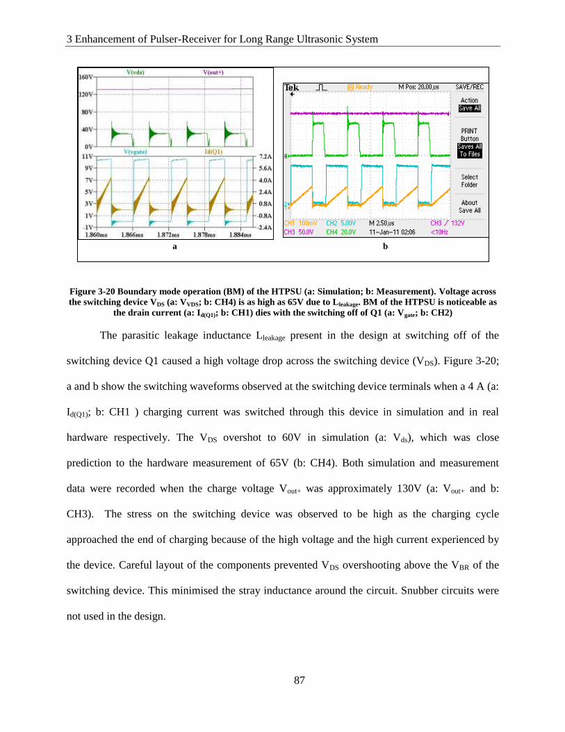
3 Enhancement of Pulser-Receiver for Long Range Ultrasonic System
87
Figure 3-20 Boundary mode operation (BM) of the HTPSU (a: Simulation; b: Measurement). Voltage across
the switching device VDS (a: VVDS; b: CH4) is as high as 65V due to Lleakage. BM of the HTPSU is noticeable as
the drain current (a: Id(Q1); b: CH1) dies with the switching off of Q1 (a: Vgate; b: CH2)
The parasitic leakage inductance Lleakage present in the design at switching off of the
switching device Q1 caused a high voltage drop across the switching device (VDS). Figure 3-20;
a and b show the switching waveforms observed at the switching device terminals when a 4 A (a:
Id(Q1); b: CH1 ) charging current was switched through this device in simulation and in real
hardware respectively. The VDS overshot to 60V in simulation (a: Vds), which was close
prediction to the hardware measurement of 65V (b: CH4). Both simulation and measurement
data were recorded when the charge voltage Vout+ was approximately 130V (a: Vout+ and b:
CH3). The stress on the switching device was observed to be high as the charging cycle
approached the end of charging because of the high voltage and the high current experienced by
the device. Careful layout of the components prevented VDS overshooting above the VBR of the
switching device. This minimised the stray inductance around the circuit. Snubber circuits were
not used in the design.
a b

3 Enhancement of Pulser-Receiver for Long Range Ultrasonic System
88
This circuit was designed to operate in boundary mode (BM) where optimal efficiency
can be achieved in flyback topology (Basso 2008). In this mode the drain current (Id(Q1)) drops to
zero with the switching signal that turns on and off the device. This behaviour is noticeable in the
simulation results presented in Figure 3-20; a, where Id(Q1) dies with the switching signal Vgate.
This mode helps reduce transition losses occur during switching and allows efficient transfer of
energy at switch Q1 opening. Measurement on real hardware presented in Figure 3-20; b –
validates this as CH1 (the voltage across the current sense resistor (Figure 3-17;R4) of value 27
mΩ, revealing Id(Q1)) reaching 0V with switching signal CH2.
Figure 3-21 The average drain current (Id) passing through the switching device Q1 as the charging cycle is
closer to the completion (simulation data).
The average primary current INMOS_AVG was calculated as 1 A (see Table 3-8), however in
simulation it was found to be as high as 1.5 A as shown in Figure 3-21. The average current
through Q1 is greatest as the output is nearing the full charge, due to a decrease in switching
frequency at this stage. The higher rated MOSFET (150V; 6.7 A) chosen as a switching device in
this design can handle the stress imposed by the high voltage level spikes of 65V and higher

3 Enhancement of Pulser-Receiver for Long Range Ultrasonic System
89
current conduction. The output diodes were chosen as recommended by the manufacturer’s
datasheet (LT3751 2008) for its fast reverse recovery time (<100 ns) while satisfying the average
current requirement.
Loading effect on power supply
Figure 3-22 Loading of HTPSU with 1.8 A load current when Vout+ and Vout- are charged to ±150V (top:
square pulse; bottom: tone burst) in simulation. With a tone burst a voltage drop of 3V was experienced

3 Enhancement of Pulser-Receiver for Long Range Ultrasonic System
90
The loading effect on the power supply output voltages when 1.8 A was drawn from it for
1 ms was simulated firstly with a square pulse as shown in Figure 3-22; top, and then with a
tone burst of a sine wave of pulse duration 1 ms as shown in Figure 3-22; bottom. In both cases
the drop in the output voltage rails was kept above 120 V; as required to satisfy the PSRR of the
transmit circuit.
Power Budget Analysis
The simulation results on power performance of the HTPSU are presented in Table 3-9. It
includes the power dissipation across the main components together with the values for the
power input and power delivered to the capacitor bank HT-Bank. An efficiency of 73 % is
predictable from this data. This is comparable with the achievable efficiency of 70% for flyback
topology (Christophe 2008) in general.
Description Average Energy in 3 seconds
Energy drawn from the input voltage source EIN 273.7 W x 3 s = 821.1 J
Power consumption of major components
Controller IC 1.38 W
NMOS switching device 11.2 W
Output diodes 2.76 W
Sense resistor R4 11.29 W
Feedback resistor R5 2.35 W
Transformer T1 6.00 W
Other 4.00 W
Total power consumption by the circuit PCONSUMPTION 38.98 W
Total energy consumed by the circuits ECONSUMPTION 38.98 w x 3 s = 116.94 J
Energy delivered to capacitor bank
CBANK+ 303 J
CBANK- 303 J
Total energy delivered to capacitor bank ELOAD 606.0 J
Energy unaccounted for (EIN – (ECONSUMPTION + ELOAD)) 32.72 x 3 = 98.16 J
Efficiency (100 * ELOAD/EIN) 73.8 %
Table 3-9 Flyback High voltage power supply efficiency

3 Enhancement of Pulser-Receiver for Long Range Ultrasonic System
91
3.5 Power budgeting and battery modelling
The operational time of the pulser-receiver unit is severely constrained by the available
amount of energy in its primary power source – the Lithium-Ion battery. A battery based on
Lithium-Ion (Li-Ion) chemistry was preferred in this application due to its high energy density
compared to other rechargeable battery chemistries such as lead-acid, nickel-metal hydride and
nickel-cadmium. The nominal open circuit terminal voltage of a single cell Li-Ion battery can
vary depending on the cathode and anode materials used in the cell. This application used a Li-
Ion battery aided with a lithium-nickel-manganese cobalt (NMC) oxide cathode and graphite
anode, with open circuit nominal and maximum terminal voltages of 3.7 V and 4.2 V
respectively. Maximum terminal voltages, in multiples of 4.2 V can be achieved by series
connecting these cells.
Due to the complex electro-chemical reaction in a Li-Ion battery, its behaviour in terms
of delivery of energy is non-linear and it can vary with the battery’s age, discharge rate and the
temperature that the cells are exposed to (Rao, Vrudhula & Rakhmatov 2003). Hence an
adequate battery model is necessary to reliably predict the number of complete LRUT cycles that
can be performed before the battery terminal voltage drops below the operational voltage.
Battery capacity is universally specified by the unit Amp-hour (Ah). Knowing the current
drawn by the system for a particular functionality, and the discharge duration, allows one to
compute the required energy capacity in Ah. Main functionalities of interest in one LRUT cycle
are depicted symbolically in Figure 3-23. The description of the functions is tabulated in Table
3-10. Discharge current levels for each function were derived from the transient simulations of
the subsystems, except for the digital circuitry. Datasheet values were used for computing the

3 Enhancement of Pulser-Receiver for Long Range Ultrasonic System
92
digital circuits’ power consumption. Note that the battery current level or function duration were
not drawn to scale.
Figure 3-23 Sequence of battery current in one LRUT cycle
A fully charged battery in the pulser-receive unit is expected to last 12 complete LRUT
cycles, referred to as test-1, test-2, etc., in Figure 3-23. Each LRUT cycle would step through
activities from function A to F. Based on this, a power budgeting table was computed as shown
in Table 3-11 and the required capacity of the battery that can adequately provide energy for 12
complete LRUT cycle was estimated as 6.5 Ah. The simulations and estimations were based on
15V power source.
Fu
nct
ion
A
Cu
rre
nt
con
sum
pti
on
- (
A)
Estimated time elapse – in seconds
Fun
ctio
n B
Fun
ctio
n C
Function D
Function E
Function F
Test 2 -> Test 1 ->

3 Enhancement of Pulser-Receiver for Long Range Ultrasonic System
93
Function Description
Function A Operator setup time. This can vary from operator to operator and location to location. Typical duration is 2 minutes, and the unit’s standby current is estimated 300 mA based on quiescent current values of the major components.
Function B Pumping of transducer array bladder, for appropriately clamping the transducers to the test specimen. This function lasts for approximately 2 minutes and the current draw is 3 A.
Function C Charging of capacitor bank of value 1600 μF x 2. This function lasts for 3 s, and a maximum of 4A is likely to be drawn from the power source.
Function D Once the capacitor bank is charged up, it is kept in regulator mode for the rest of the test which can be as long as 2 minutes. Simulations revealed the current drawn for this operation is about 0.75A.
Function E Data collection; transmit and receive cycle repeated 16 times within one LRUT cycle in a typical application. Both activities are approximated to last 2 minutes simultaneously with function D. Receive activity draw about 2 A, based on 10 W power consumption and 5 V supply.
Transmit activity during excitation of transducers, has been accounted for in function D. However the quiescent power consumption was not accounted for which can draw 10 mA per channel for the duration of 2 minutes.
ADCs are on during this period, sampling the received data consuming 3W power.
DACs are turned on for during this period, consuming 3W dynamic power for 1.1ms and static power of 0.1W (3.3V x 30 mA) for the rest of the period.
Function F Digital electronics – this is considered static, and calculations based on datasheets extracted values, this function consumes about 10 W with a supply voltage 3.3 V, so 3 A is assumed to be drawn for this function for the complete LRUT cycle.
Table 3-10 function description
Modelling of the battery
A suitable model for simulating this battery behaviour was researched to allow an
estimation of the final battery terminal voltage after each LRUT cycle. Various models for Li-
Ion batteries ranging from an analytical/mathematical model (Pedram & Wu. 1999), (Rakhmatov
& Vrudhula 2001), (Rakhmatov 2005) to abstract models (Benini et al. 2000), (Kroeze & Krein
2008), (Gold 1997) have been cited in the literature. All these models had been critically
reviewed by (Rao, Vrudhula & Rakhmatov 2003) highlighting the strengths and weakness of the
models, together with their model descriptions. The Li-Ion battery model published by Gold
(Gold 1997) is an electrical model, based on an E-Value ABM elements and discrete resistor and

3 Enhancement of Pulser-Receiver for Long Range Ultrasonic System
94
capacitor models. This model was written in PSpice, which can be simulated in the LTSpice
environment and allows simulating battery charging behaviour, discharge behaviour, battery life-
cycle and temperature effects on the battery. This published work was claimed to be 88%
accurate and the description of the model is very well documented in (Rao, Vrudhula &
Rakhmatov 2003) and (Gold 1997). The model uses lookup tables which were formulated with
values obtained by characterising a Li-Ion battery cell Polystor ICR018650, which has a design
specification of 1.25 Ah with 4.2V (Max) 3.6 V (Nominal) and 2.75V (cut off) voltage with a
cell series impedance of 80 mΩ.
Function Description Current
consumption
Duration in seconds As As
24channels
Ah
Function A Operator setup time ~300 mA 120 s x 12 432 - 120E-3
Function B Collar inflation ~3 A 120 s x 12 4320 - 1.2
Function C Initial High voltage
bank charge up
4 A 3 s x 12 144 - 40E-3
Function D High voltage bank
regulation mode
0.75 A 120 s x 12 1080 - 300E-3
Intermediate charging
between averaging
4A 10 ms x 16 x 12 7.68 - 2.2E-3
Function E Receive circuit
(allowed 1s per shot)
10 W/5V = 2 A 16 s x 12 384 9216 2.56
Transmit circuit
standby
10 mA 120 s x 12 14.4 345.6 96E-3
ADCDYNAMIC –
assumed on throughout
140mW/3.3 =
42 mA
120 s x 12 60.5 1451.5 0.4
DACDYNAMIC 120mW/3.3 =
36 mA
1.1ms x 16 x12 7.6E-
3
0.183 0.05E-
3
DACSTATIC 30 mA 120 s x 12 43.2 1036.8 288E-3
Function F Digital electronics 12 W/3.3 V =
3.6 A
120 s x 12 5184 5184 1.44
Total Approximated 6.5
Table 3-11 Power budgeting table

3 Enhancement of Pulser-Receiver for Long Range Ultrasonic System
95
Figure 3-24 Equivalent circuit model of the battery pack resembling the prototyped battery pack. Each cell is
an exact model of (Gold 1997) and parameterised to match Teletest battery pack. Load is provided by a
current source.
A simulation model of the required battery pack was developed by arranging the
simulation model of Li-Ion battery cell Polystor ICR018650 in 4 parallel by 4 series arrangement

3 Enhancement of Pulser-Receiver for Long Range Ultrasonic System
96
as shown in Figure 3-24. Each cell is an exact model published by (Gold 1997) and
parameterised to match prototyped/ specified battery pack. This arrangement in effect forms a
simulation model for a 5 Ah, 14.4 V (nominal) battery pack. A decision to use an open circuit
nominal terminal voltage of 15 V for the Li-ion battery was made, based upon the dimension of
battery cells in the market that will fit the physical constraints of the prototyped product. A
simple current source model (Figure 3-24; Discharge) was used for loading the battery pack
during simulation. This model can be inputted with a stimulus data file, which represents the
battery discharge current data recorded during measurement or compiled using data obtained by
simulating the system constructs. This stimulus data resembles the sequence of the battery
discharge current pattern shown in Figure 3-23 for one LRUT cycle. Usage of this model avoids
the need of including all simulation models developed for simulating the loading effect on the
battery, hence simplifying modelling, which speeds up simulation.
Figure 3-25 Imitated discharge current loading the battery pack simulation model

3 Enhancement of Pulser-Receiver for Long Range Ultrasonic System
97
Figure 3-25; top, shows in simulation, how the terminal voltage of the developed battery
model drops with discharging when it was loaded with repeated discharge data. Here the
discharge data input was compiled using the data obtained from previous simulations and
predictions. The same discharge cycle/pattern was repeated 12 times as shown in Figure 3-25;
bottom, where the pattern of the IDischarge1 waveform is periodic of the LRUT cycle, having
attributed as Figure 3-23. It is noticeable from Figure 3-25; top, the battery model showed a
terminal voltage of approximately 15.8 V initially and after 12 LRUT discharge cycles, it
dropped down to a lower value of approximately 14.6 V. The high 13 A current spike at the
beginning of each LRUT cycle is expected to occur every time the pump that inflates the
transducer array is started (see section 2.3). This high spike in reality lasts for 100 ms (not visible
due to the high time base setting on the plot) and pulls the battery terminal voltage down which
is the likely reason for tripping/collapsing the battery terminal voltage. This is also noticeable on
the graph.
Evaluation of the model
Evaluation of the battery model was carried out by firstly recording the current
draw/discharge trend when the prototyped battery pack was loaded with the real hardware of a
prototyped pulser-receiver, and then the recorded data was inputted in the simulation via a
current source shown in Figure 3-24; discharge1, so that the developed simulation model is
loaded with the real measurement data instead of the compiled data used in the previous
simulation. The results are presented in Figure 3-26, showing the final battery terminal voltage
dropping down to approximately 14.8 V after 12 repeated LRUT cycles. This final battery
terminal voltage is in reality higher than the theoretical minimum battery terminal voltage 13.3 V

3 Enhancement of Pulser-Receiver for Long Range Ultrasonic System
98
possible according to the cell manufacturers. Hence, the simulation was extended to foresee the
maximum complete LRUT cycles possible before the battery collapses.
Figure 3-26 Real hardware loading effect on the Li-Ion battery simulation model
Figure 3-27 Number of completed LRUT cycles in simulation
Battery terminal voltage at
the end of 12th LRUT cycle
LRUT cycle 1 and initial
battery terminal voltage
Pump start-up current HVPSU start-up current for
charging HT-Bank
16 averaging of LRUT data
collection
Failure due to lack of power

3 Enhancement of Pulser-Receiver for Long Range Ultrasonic System
99
Figure 3-28 Number of completed LRUT cycles and battery terminal voltage drop
Extended simulations carried out had the number of LRUT cycles extended to more than
12, as shown in Figure 3-27. It shows the possibility of executing 16 complete LRUT cycles
before the battery terminal voltage terminates/collapses. This is indicated by the red-dashed
lines. In reality 15 shots were achieved with the prototyped hardware and a fully charged, brand
new battery. The measurement results together with the simulation data are presented in Figure
3-28.
3.6 Hardware realisation
The hardware discussed was prototyped, and eventually has been launched as a
commercial product. The prototype development of the power electronics circuits and the
primary power source – the battery for the pulser-receiver unit used system modelling techniques
for the design process. It allowed prototypes to be produced with very minimal resources used,
12.5
13
13.5
14
14.5
15
15.5
16
16.5
17
0 2 4 6 8 10 12 14 16 18
Bat
tery
te
rmn
al v
olt
age
(V
)
Test Number
Prototype Battery Terminal Voltage Drop testNumber of Reliable Tests
Simulation: start terminal voltage (estimated) Simulation: Finish terminal voltage (estimated)
Simulation: Start terminal voltage (real hardware) Simulation: Finish terminal voltage (real hardware)
Measurement: Start terminal voltage Measurement: Finish terminal voltage

3 Enhancement of Pulser-Receiver for Long Range Ultrasonic System
100
avoided over-specified component selection and reduced design iterations. This section includes
some of the traces obtained during the prototype development.
3.6.1 PSU prototype
Figure 3-29 Power electronics hardware for pulser-receiver unit
The power electronics circuits of the pulser-receiver were designed to produce power
levels + 5 V; 12 A, -5 V; 2 A, +24 V; 1 A, -24 V; 1 A, 12 V; 12 A and a ±150 V high voltage
power supply. Figure 3-29, shows the power supply hardware that generates all these power
Switch mode power supplies
+/- 150V
- 5 V @ 2 A
+ 5 V @ 12 A
-24 V @ 1 A + 24 V @ 1 A + 12 V @ 12 A

3 Enhancement of Pulser-Receiver for Long Range Ultrasonic System
101
levels from a 15 V (Nom); 5.3 Ah Li-Ion battery, with the traces captured during the prototype
testing of all the mentioned power supply domains. The traces show their corresponding output
voltage level while drawing the maximum current that each power supply was designed to
handle. The hardware performed satisfactorily and did not require design iteration.
The prediction of the HT-Bank capacitance value and the battery capacity during the
study allowed the prototype to be designed in a compact form as shown in Figure 3-30, which
allowed the pulser-receiver unit to be designed with a one third reduction in weight and size
without compromising the performance or operational length of time. Note that the capacitance
value for HT-Bank is the same for the previous version of the pulser-receiver but the research
work and the system level simulation allowed confirmation of its value which was impossible
otherwise.
Figure 3-30 HT-Bank together with its associated transmit and receive circuit

3 Enhancement of Pulser-Receiver for Long Range Ultrasonic System
102
Figure 3-31 Pulser-receiver unit as a commercial product
A commercial product was manufactured based on the prototype. Figure 3-31; left and
right, shows the size comparison between the latest and the previous version of the pulser-
receiver units. Practical tests carried out on the manufactured pulser-receiver unit revealed a fully
charged battery of specification 15 V (Nom); 5.3 Ah allows 20 complete inspection cycles. This
satisfies the predicted performance of 12 inspection cycles stated above. An increase in the
number of LRUT cycles in the production version was due to the enhanced pump assembly and
the reduction in standby/ setup time achieved by means of the software enhancement. The new
pump assembly only takes about half the time to inflate the collar compared to the time taken by
the previous pump assembly and the predicted 2 minutes in the calculations. Software
enhancement increased the speed of transferring data to the PC, and provided an easy to use
graphical interface for rapid setup and configuration.
3.7 Summary
This Chapter has described building a custom simulation tool box that can be used in the
design process for product enhancement. Once it was built it was then fully utilised to analyse
MK4 unit MK3 unit
MK4 battery MK3 battery

3 Enhancement of Pulser-Receiver for Long Range Ultrasonic System
103
power and functional performance of the system against industrial requirements. The goal of
enhanced portability was achieved, with efficient usage of resources.
The choice of model topology and relaxing of simulation settings were found to be a
valuable tactic in the development and simulation of this tool set for achieving acceptable
accuracy and to overcome non-convergence issues experienced especially because of its non-
linear circuits. Full-featured topology specific models were found to be accurate but difficult to
simulate. On the other hand, equivalent circuit models were also found to be equally useful and
produced acceptable simulation results, despite their lower accuracy. However, the accuracy of
the topology specific models, especially those used in the modelling of the power supply circuits
and the transmit circuits, provided a powerful tool for debugging and observing component
specific issues at the prototype and maintenance phases, and subsequent prototyping of the
circuits generated from the modelling work.
The research enabled the instrumentation utilised in the LRUT application to be assessed
for its power performance for various load conditions and variants of hardware configurations.
This work made it possible to reliably specify a suitable primary power source for PI’s flagship
product Teletest®, well before the hardware had been developed. To produce sensible simulation
results that can be utilised in the process of evaluating the portability enhancement the following
assumptions and compromises were made:
1. Model evaluation against measurement data at component level was minimal. Obtaining
measurement data for validation at a component level suffered, because of limited
resources and unavailability of hardware at the early stages. Instead, expert knowledge in
the form of measurement data obtained from previous hardware in separate work,

3 Enhancement of Pulser-Receiver for Long Range Ultrasonic System
104
subsystems’ specifications and theoretical calculations were used for model evaluation.
This was accepted as adequate for two major reasons; first most models used in the
development of all power sensitive sub circuits were topology specific models and were
assumed accurate, second the equivalent circuit models developed for two main
components – the battery and the transducer, which strongly influenced the decision
making, were validated against measurement data. The prototyped power supply designs
were also validated using measurement data.
2. Downsizing the primary power source – the battery was identified to be the only possible
option for enhancing portability of this system. Computation of power consumption data
of the system was required for allocating a suitable power source. It assumed a worst case
scenario on every single active cycle of the system for computation of the average power
computation. This was conservative to account for possible inaccuracies in the model
development and any human error possible in operation.
3. A smaller size and less weight of the Li-Ion battery pack were only possible with a lower
battery capacity. Capacity reduction introduced potential risks of shortening operational
time and functional performance, by limiting the battery cells’ ability to handle a high
rate of change of discharge current. In essence, it was the battery terminal voltage that
needed to be maintained above the required minimum operational voltage of the system,
for any possible discharge current rate the system imposed on the battery. With the
available battery cells in the market it was possible to stack a number of standard cells in
a serial-parallel combination to achieve the required terminal voltage and capacity.
4. A model accuracy of 20% was accepted for the transducer equivalent circuit models and
efforts were made to produce simulation data that agreed with the measurement data

3 Enhancement of Pulser-Receiver for Long Range Ultrasonic System
105
within the application range. These attributes somewhat limit this model’s ability to adapt
or assess hardware for future application enhancements. The system modelling rule of
including only what is needed in the simulation model was followed to guarantee success
of achieving the goal on time. The models produced are suitable for immediate future
applications regardless. Further work on refinement of the equivalent circuit model of the
piezoelectric element, and the Teletest transducer is recommended for ease of
parameterisation and gaining confidence on its accuracy. The same argument applies to
the battery model used; although the data used in the model were not produced for the
exact battery cell used in the real hardware, the model provided a close prediction. The
LRUT instrumentation is likely to use the chosen battery cell with variants of
combinations in its future designs. Hence characterisation of the very battery cell used in
the custom battery made is encouraged for the refinement of the model.
5. Simultaneous simulation of all developed models in a single simulation platform was not
performed to avoid complexity and improve simulation time. This simplification was
assumed acceptable, because the subsystems that affected the battery behaviour
differently when connected to another subsystem were simulated simultaneously with
other relevant subsystems to capture the difference. Simulating the drive circuits with a
transducer array allowed analysing and producing data on these circuits’ dependency on
load behaviour. The utilisation of this data in the specification of the high voltage power
supply for the drive circuits (HTPSU) has proved essential to maintain PSRR of these
application critical circuits.
6. The modelling work explored the possibility of including a feature of analysing the port
dynamics of the LRUT instrumentation by closing the loop between the transmit and

3 Enhancement of Pulser-Receiver for Long Range Ultrasonic System
106
receive sides of the system, by the inclusion of the electro-acoustic nature of the medium.
This is discussed in Chapter 4. It was appreciated that it is almost impossible to model
and simulate the acoustic nature of the medium on which the LRUT technique is applied
in PSpice, however efforts were made to demonstrate the ability of the developed model
to adapt to include abstract information of components, with the functionality to model
coupling between two or more engineering disciplines.
The outcome of this part of the research is three fold; firstly, an adequate battery that
allows reliable LRUT inspection for the planned period of 12 hours/ 12 tests, while improving
the portability by 33% in size and weight, secondly the process allowed rapid prototyping of
LRUT hardware sustainably and thirdly, the model provided a platform on which variants of this
hardware can be assessed with no concern of damaging or utilising useful resources. However,
this work has identified the need for a platform free template with all necessary formulae to
provide information on battery capacity requirements for variants of hardware configuration.
This would benefit the industry, where expert knowledge is not always available to use the
simulation tool. Initial work on this had been demonstrated with an Excel based template, where
the built-in formulae were obtained, using a curve-fitting method on the obtained power
performance graphs produced from simulation data.

107
4 MEDIUM FREQUENCY LRUT APPLICATION – SYSTEM MODEL REUSE
4.1 Overview
One of the efficient features of using a system modelling technique is the ability to reuse
the developed system model for verifying and/or studying new concepts and to thereby
accelerate the design process with minimal resource usage. This Chapter introduces one such
application in which the system models that were developed for power performance analysis in
Chapter 3 were redeployed for evolving the existing low frequency LRUT process and hardware
to its next phase of a medium frequency application for inspecting complex structures. This
design process required rapid prototyping to prove the concept.
4.2 Medium frequency LRUT application
LRUT of complex structures such as aircraft components is challenging as the reflection
from the features becomes more complex and harder to analyse. This research programme
looked at inspecting one such complex component used in the aircraft wing assembly, which
experiences high and variable stresses in operation, leading to potential fatigue cracking, but has
limited access for inspection and maintenance. This component is graphically shown in Figure
4-1 with possible locations for mounting transducers for LRUT inspection using pulse-echo or
pitch-catch methods. The Finite Element Analysis (FEA) carried out and published by (Haig &
Stavrou 2012) reports, for reliably detecting flaws in these type of complex structures, the LRUT
technique utilising an ultrasonic wave frequency in the high 100’s of kilohertz is required, in
contrast to the low frequency LRUT application employed in pipeline inspection.

4 Medium frequency LRUT application – System Model reuse
108
Figure 4-1 Complex structure of an aircraft wing assembly component (Haig & Stavrou 2012)
4.3 Reusability of existing hardware
The complex features of the aircraft components require a medium frequency ultrasonic
wave-mode in the frequency range of 300 kHz and 1 MHz for inspection as (Haig & Stavrou
2012) proved using FEA modelling. The transmit and receive circuit in the pulser-receiver unit
discussed in Chapter 3; section 3.3.1 and section 3.3.3, respectively were designed for low
frequency applications and cannot handle the higher frequencies proposed by (Haig & Stavrou
2012) for experimental work i.e. in the range of up to 1 MHz. The project required rapid
prototyping of a medium frequency instrument.
The existing hardware, discussed in Chapter 3 was assessed first and then the feasibility
of modifying its circuits to serve this purpose was analysed. This was carried out by means of
simulation using the developed LRUT system models discussed in Chapter 3. Once suitable
component and/or circuit changes were identified the corresponding components in the
Pair 4
Region For Potential Crack
Pair 3
Monolithic in-plane shear transducer
Receiver
Monolithic in-plane shear transducer
Transmitter
Monolithic in-plane shear transducer
Receiver
Monolithic in-plane shear transducer
Transmitter
Pairs 1 & 2
Co-located 1-3 composite transmitter
and receivers

4 Medium frequency LRUT application – System Model reuse
109
developed simulation models were replaced with the new models and simulated for validating
component and/or design changes.
4.4 Development of high frequency transmit circuits
Figure 4-2 Medium frequency LRUT hardware architecture
The proposed hardware for the medium frequency LRUT experiment is shown in Figure
4-2, where a single transmit channel is multiplexed to four individual LRUT-transducers using
DPST (Dual Pole Single Throw) relay switches. The control electronics switches the relays in
the following manner; the transmit circuit excites one of these transducers while the other three

4 Medium frequency LRUT application – System Model reuse
110
transducers are switched to three of the four receive circuits, receiving the reflected signal from
features such as flaws and edges of the test specimen.
The LRUT-transducers discussed in Chapter 3; section 3.2.2, were used. Rapid
prototyping was carried out by firstly simulating the concept in the LTSpice computer
environment utilising previously developed LRUT system models with suitable modifications to
transmit, receive and the power supply electronics. The digital logic for control, waveform
generation and data storage was facilitated using commercially available data acquisition
instrumentation from scientific hardware manufacturer National Instruments.
4.4.1 Transducer model and its performance
This particular application requires a single LRUT-transducer to be excited with an
electrical excitation signal with a frequency in the range of 10 kHz and 1 MHz and with a
maximum amplitude of ±80V. The input impedance analysis carried out reveals the drive
electronics is likely to drive a load impedance of 148Ω at 1 MHz, which is equivalent to 1.3 nF
in capacitance value at 1 MHz, considering 20% tolerance on the LRUT-transducer impedance.
The impedance characteristics of the LRUT-transducer, showing the impedance values
for the extended frequency application of 1 MHz, are shown in Figure 4-3. Both simulation and
measurement results obtained using an impedance analyser are presented with error bars set on
each experimental data point. Error bar setting on the impedance curve and the phase curve are
set to ± 20% and ± 2% respectively. Simulation results deviate from the measurement results by
nearly 40 % at the high frequency end. Optimisation of the model was not considered for the
following reasons; the model accuracy was proved to be acceptable in the previous application

4 Medium frequency LRUT application – System Model reuse
111
discussed in Chapter 3 and the impedance values for 80% of the frequency range of interest
agree with the measurement data with moderate accuracy of around 30% closer to the end.
Figure 4-3 Impedance characteristics of an LRUT transducer for extended 1 MHz application
An appropriate drive circuit (transmit) was required to sufficiently excite an LRUT-a
transducer for the frequency range 20 kHz – 1 MHz at ± 80V.
4.4.2 Medium frequency transmit circuit
Parameter Symbol Value
Supply voltage VS ±100VDC
Excitation signal frequency FEXT Min = 20 kHz; Max = 1 MHz
Excitation voltage VEXT ± 80 V (Peak ≅ 80 V)
Load CLOAD Maximum of 1 LRUT-transducers ~ 1.3 nF
Input to transmit circuit VIN Von-Hann windowed Sine wave (20 kHz to 1 MHz)
Voltage gain GPA Adjustable – default 27 dB
Table 4-1 Medium frequency transmit circuit specification
1882Ω
207Ω
1460Ω
148Ω
-120
-100
-80
-60
-40
-20
0
1.E+00
1.E+01
1.E+02
1.E+03
1.E+04
1.E+05
1.E+06
Ph
ase
(°)
Imp
edan
ce (Ω
)
Excitation frequency (Hz)
LRUT-Transducer impedance characteristics curve at higher
frequencies
Impedance - practical Impedance - simulation
Phase - practical Phase - simulation

4 Medium frequency LRUT application – System Model reuse
112
The specification of a transmit circuit for facilitating medium frequency LRUT is given
in Table 4-1. Design specific calculations are included in Table 4-2 for component selection and
evaluation (Cirrus logic 2009).
Parameter Formula Value
Slew Rate (SR) 𝑆𝑅 = 2 × 𝜋 × 𝐹𝐸𝑋𝑇 × 𝑉𝐸𝑋𝑇_𝑀𝐴𝑋 × 1 × 10⁻⁶ 630V/μs
Total load Impedance (XC) 𝑋𝐶 = 1 (2 × 𝜋 × 𝐹𝐸𝑋𝐶𝐼𝑇𝑀𝐴𝑋× 𝐶𝐿𝑂𝐴𝐷)⁄ 148 Ω ± 20%
Peak load current (IPEAK) 𝐼𝑃𝐸𝐴𝐾 = 𝑆𝑅 × 𝐶𝐿𝑂𝐴𝐷 0.8 A
Worst case power dissipation
(PTX_WORST) 𝑃𝑇𝑋_𝑊𝑂𝑅𝑆𝑇 = 4 × 𝑉𝑆
2 2 × 𝜋 × 𝑋𝐶⁄ 53 W
Table 4-2 Medium frequency transmit circuit calculations
Satisfying the required functional specification to sufficiently excite the LRUT transducer
at 1 MHz cannot be met by the transmit circuit discussed in Chapter 3; section 3.3.1, because of
the slow slew-rate of the power amplifier used in the circuit (300 V/μs), despite its ability to
comfortably satisfy output voltage and load current requirement. The LTSpice simulation model
developed for the transmit circuit previously, allowed individual components to be evaluated for
their performance when integrated in the circuit design, due to the topology specific modelling
methodology followed in the model development of this circuit.
The slew-rate limited power amplifier model in the existing transmit circuit (Chapter 3;
section 3.3.1) was replaced with a suitable power amplifier model with necessary modification in
the circuit and simulated for the circuit and component functional performance. The circuit
diagram is similar to the simplified circuit shown in figure 3-8, which shows the off-the-shelf
power amplifier and the complementary MOSFET circuit with over-current protection. The
power amplifier used is capable of delivering 5 A pulsed current. However, the complementary
MOSFET circuit was left in the circuit as a buffer to protect the power amplifier, should a short
circuit occur in the load. The power amplifier utilised does not have integrated overcurrent
protection circuit.

4 Medium frequency LRUT application – System Model reuse
113
Figure 4-4 Bode plot of the medium frequency transmit circuit in simulation
Both AC and transient analysis were carried out to make sure an undistorted performance
is achieved. Figure 4-4 shows the frequency response of the modified transmit circuit, depicting
its ability of handling the application specific frequency range of up to 1 MHz without distortion.
A set gain of approximately 27 dB was maintained for the entire frequency range. The phase
value of 180° represents the inverting amplifier configuration.
Transient analysis at the output of the modified transmit circuit model was obtained by
simulating the model with an input signal of amplitude ± 4.3V and frequency 1 MHz. With this
input amplitude and the gain set to 27 dB, an output of 96V is achievable at the output of the
transmit circuit (ignoring voltage drop across devices). An undistorted excitation signal of
approximate amplitude of ±90V and frequency 1 MHz was observed in simulation as shown in
Figure 4-5; a. A voltage drop of approximately 7V was noticed across the complementary
MOSFET pair as expected. The output current delivered to the load was observed to be as high

4 Medium frequency LRUT application – System Model reuse
114
as 700 mA. In both frequency and transient analysis simulations the LRUT-transducer model
discussed in Chapter 3; section 3.2.2 was used as a load.
Figure 4-5 Excitation signal driving LRUT-Transducer showing 190Vpk-pk; at 1 MHz (a: simulation; b:
measurement)
The circuit was prototyped and the output waveform observed, as shown in Figure 4-5; b.
It is noticeable that this waveform matches the simulation results; amplitude ±90 V and
frequency 1 MHz.
4.4.3 Medium frequency receive circuit
The receive circuit requirements for this application were specified to have a selectable
gain of 20 dB or 40 dB, with a bandpass filter having cut-off frequencies of 150 kHz and 1.2
MHz, so that a flat response can be achieved for the frequency range of interest between 300 kHz
and 800 kHz as reported by (Haig & Stavrou 2012). The receive circuit discussed in Chapter 3;
section 3.3.3, is not adequate to facilitate the required high bandwidth specification as it was
designed to handle input signal frequencies of up to 100 kHz for a typical LRUT application on
pipes. The simulation model developed for the receive circuit was modified with appropriate

4 Medium frequency LRUT application – System Model reuse
115
components and simulated before prototyping. The frequency response obtained in simulation
(shown in Figure 4-6) reveals the ability of the receive circuit to meet the specification of
approximately 37 dB gain and cut-off frequencies for high-pass and low-pass filters at 150 kHz
and 1.2 MHz respectively. This simulation was setup with a gain setting of 40 dB and the
reduction in amplification (~ 3dB) was due to the passive filter arrangements.
Figure 4-6 Bode magnitude plot, showing receive circuit’s performance in simulation
4.4.4 Power supplies
The power supplies discussed in Chapter 3 were used with appropriate modifications,
specifically to the capacitor bank (Cbank+ and Cbank-) used in the high voltage power supply
37.49dB
0
5
10
15
20
25
30
35
40
Re
ceiv
e G
ain
, d
B
Receive signal frequency, Hz
High frequency receive circuit Bode plot
Receive_gain = 40dB -3dB line

4 Medium frequency LRUT application – System Model reuse
116
discussed in section 3.4.1. In this application a 100 μF capacitor was used on the +Ve and –Ve
rails of the high voltage power supply to provide a ripple-free supply to the transmit circuit.
Simulation work was carried out using the developed simulation model of the high voltage
power supply, but not presented in this section as it is similar to the previous work discussed in
Chapter 3; section 3.4.1. However, the usage of the developed simulation model for verifying the
design suitability for the application was demonstrated. In this work the high voltage power
supply HTPSU was required to produce ± 100V. The ± 24V power supplies were modified to
provide ± 15V DC supply for the input stages of the transmit circuit.
4.4.5 Typical system level simulation
This section outlines an investigation of the possibility of integrating the test specimen in
the system model so that the receive signal strength at the receive ports of the pulser-receiver for
a known transmitted signal strength can be observed in simulation. Modelling the medium and
integrating in the simulation enables a study and consequently a definition of the port dynamics
of the pulser-receiver unit. Accuracy depends on the accuracy of the model of the test specimen.
The medium in most cases is a metallic component, for which the acoustic-mechanical property
and the coupling between them are difficult to model in the electrical domain but very easily can
be modelled in the EDA tools like Abacus (Avolution 2008) – a popular modelling tool for
modelling acoustic and mechanical properties of materials. This research work was restricted to
electrical simulation tool LTSpice and effort had been made to model the test specimen based on
the work carried out by (Scott & Philip 2008) for wirelessly powering in situ structural health
monitoring systems embedded within aircraft and other high value engineering assets. He used
lossy transmission line models to model the electro-mechanical behaviour of the system.

4 Medium frequency LRUT application – System Model reuse
117
The developed simulation models for a LRUT-transducer, transmit circuit and receive
circuit were integrated with a simulation model for the medium (aluminium plate). This
simulation demonstrates the ability of the system model in simultaneously simulating multi-
engineering domain constructs for validation. The aluminium plate was modelled using a lossy
transmission line model. The features of the aluminium plate were not included. Parameters used
in this modelling are included in appendix A.
Figure 4-7 Multi-engineering domain system simulation of the medium frequency circuits
The high voltage power supply, HTPSU was not included in this simulation for the
purpose of minimising simulation time and computing resource usage. This setup was used to
simulate pitch-catch LRUT, using piezoelectric transducer models U15 and U14 as a transmitter
and receiver respectively. The transmitted signal propagates through the test specimen Q3-Q1-

4 Medium frequency LRUT application – System Model reuse
118
Q2 from the transmitting end to the receive end. Transducers U15 and U14 are assembled with
face plates Q14 and Q15 and backing blocks R23 and R22 respectively.
The simulation results presented in Figure 4-8; a and b, show the receive signal strength,
when a single transducer – U15 was excited with a ± 100 V; 1 MHz and ±100V; 500 kHz
excitation signal respectively.
Figure 4-8 Medium frequency system simulation for excitation frequencies a: 1 MHz and b: 500 kHz
The signal received by the receive LRUT-transducer model (U14) was amplified by 20
dB at U9 and further amplified to 40 dB at U8 (40 dB in total). Wave mode separation is better

4 Medium frequency LRUT application – System Model reuse
119
when an excitation frequency of 1 MHz was utilised compared to 500 kHz. This is noticeable in
Figure 4-8; a, as the receive signal and the echo are well separated compared to their
corresponding waveforms presented in Figure 4-8; b for 500 kHz excitation. However, 500 kHz
excitation had better penetration, showing a higher receive signal amplitude in Figure 4-8; b,
compared to the 1 MHz excitation presented in Figure 4-8; a. The models used to represent the
medium are only approximate and cannot be used to predict application specific frequencies that
(Haig & Stavrou 2012) predicted by FEA modelling of the test sample using simulation tool
Abacus.
4.5 Hardware implementation and system integration
Figure 4-9 Experimental setup for high frequency LRUT on sample while developing a crack

4 Medium frequency LRUT application – System Model reuse
120
An experiment shown in Figure 4-9; a, was setup as discussed by (Haig & Stavrou 2012).
The prototyped hardware was used to condition monitor the test specimen using a medium
frequency LRUT technique in pitch-catch mode, while a crack was grown/ developed from 0
mm to 5 mm in a controlled manner. The crack developed from a notch feature as shown in
Figure 4-9; b.
Figure 4-10 LRUT excitation at 500 kHz with crack size 0 mm (a) and 5 mm (b)
Medium frequency LRUT inspection results on the test specimen, when the crack size
was 0 mm and 5 mm are given in Figure 4-10; a and b, respectively for an inspection frequency
of 500 kHz. The plots show the received amplitude (after amplification of 20 dB) on the Y-axis
and the time of arrival of the received signal from transmit time on the X-axis. It is noticeable
that the received amplitude is approximately 380 mV when the crack size is 0 mm. Comparison
of this practical results with the simulation results shown in Figure 4-8;b (250 mV) for 500 kHz

4 Medium frequency LRUT application – System Model reuse
121
is outside the acceptable accuracy when it comes to wave-mode propagation analysis but is
acceptable for the purpose of hardware development, as the order of magnitude is the same. This
is important in defining the port dynamics of the hardware.
The developed hardware is at present implemented in a test rig that is subjected to a wide
range of test/atmospheric scenarios for gathering large amounts of data for neural-network
analysis.
4.6 Summary
This Chapter discusses the development of prototype hardware for a medium frequency
LRUT application which was investigated by means of system modelling techniques. A medium
frequency LRUT application was studied as a possible method of inspecting components with
complex features. This application deployed pitch-catch mode, initially by means of exciting a
piezoelectric transducer in shear mode, and consequently transmitting high frequency ultrasound
in the 150 kHz and 1 MHz range through the test specimen of the material, aluminium. The
ultrasound is received by a second piezoelectric transducer at a different location on the same
test specimen. The LTSpice models developed in the previous Chapter were reused with
necessary modification to develop this system and simulated for specifying and evaluating
hardware. The model in particular included lossy transmission line models for representing a test
specimen and transducer face plates, which in general possess acoustic-mechanical properties.
This in effect dampens the ultrasonic wave generated by the excited transducers and resulted in
the receive signal strength being reduced. However, these models are not optimised for analysing
wave propagation analysis at present due to the dimensions and material properties used being

4 Medium frequency LRUT application – System Model reuse
122
only approximate. Measurement data on the receive strength were observed to be in the same
magnitude order as the simulation data.
The modular concept implemented in the system model development in Chapter 3
allowed relevant circuits to be modified and or enhanced without compromising the performance
of the other circuits. The developed system model provided a platform for rapid prototyping
besides the fact that the previously developed model was developed for power budgeting
analysis in the first place. More work was required on the hardware for multiplexing the channels
and optimising it for exploitation purposes, but this was not covered in this particular research
work.
As a concluding remark, a powerful tool set has been developed in this part of the
research work for future circuit enhancement, modifications and maintenance.

123
5 ELECTRON BEAM WELDING SYSTEM
5.1 Overview
This Chapter gives an overview of Electron Beam Welding (EBW) and describes the
EBW system and its operation. An application specific problem, caused by a fault condition
called flashover and its consequences is introduced, followed by a discussion on improving the
welding process, so that weld quality and the integrity of the EBW system is maintained.
5.2 Electron beam welding process
Electrons can easily be extracted from a thermionic emitter (cathode), and accelerated by
a high voltage, to convert the resulting kinetic energy involved into heat at the point of impact on
the work specimen (Fritz et al. 1998). This is the basis of Electron Beam Welding.
Conventionally electron beams are generated in vacuum (< 5 x 10⁻⁵
mbar). Vacuum provides an
insulation to avoid high voltage breakdown and protects the cathode (e.g. tungsten at 2700K) in
the EBW gun from oxidation or erosion. It also prevents the beam spreading due to electron
collision with gas molecules. Later researches showed that EBW at a reduced pressure (10-1
to
100 mbar) is also possible and has distinct advantages such as better control of weld defects
(Sanderson & Ribton 1998), (Punshon, Sanderson & Belloni 1998). Non-vacuum EBW has also
been recorded in the literature (Schulze & Powers 1998), (Fritz et al. 1998) although the inherent
scattering of electrons through collision with molecules limits NVEBW to thinner sections of
material.
The process is very popular in industrial applications such as aerospace (Russell 1981),
marine (Galsworthy & Bird 1998), nuclear waste burial (Nightinggale et al. 1998), automotive

5 Electron beam welding system
124
(Schulze & Powers 1998) and science for its high integrity, low distortion, higher welding speed,
lower heat input, and greater depth-to-width aspect ratios than many of the other fusion type
welding means (Schulze & Powers 1998), (Russell 1981), (Fritz et al. 1998). Although EBW and
Light Amplified by Stimulated Emission of Radiation (LASER) beam welding have been widely
accepted as high energy welding tools, EBW is superior to LASER in many aspects such as
penetration level and energy capacity, but has the disadvantage of requiring the component to be
within a vacuum chamber, which can reduce productivity, and requires biological shielding to
absorb the X-rays produced by the electrons being stopped. Comparison of these two welding
processes is very well documented in (Hanson 1986).
5.2.1 Electron beam Generation
Electron beam generation for material processing requires an EBW gun with a high
voltage power supply and auxiliary power supplies. The EBW gun is an electrical device that
releases a high energy electron beam when its thermionic cathode is heated and an acceleration
potential is applied between the cathode and anode electrodes. The cathode is conventionally a
tungsten ribbon filament heated using an auxiliary power supply, itself floated at the accelerating
potential. However, the electron beam group at TWI currently uses an indirectly heated diode
type gun for its more robust and long life cathode, simplified cabling and power supply
requirements. Detailed description of the EBW gun and its technical details together with the
performance are documented in (Sanderson & Ribton 1998). In essence, the main cathode
(lanthanum hexaboride) in the gun is indirectly heated by a primary electron beam source based
on a radio frequency (RF) excited (84 MHz) filament and accelerated under the influence of a
constant negative 150 kV (-150 kV) electric field. The use of RF heating allows coupling of the

5 Electron beam welding system
125
auxiliary supply for cathode heating across the gun vacuum, and precludes the need for auxiliary
supplies floated at high voltage and the associated cabling.
The kinetic energy E produced by an electron when accelerated by an electric field V is
given by Equation 5-1.The terms q, m and v are the charge of an electron (1.602E-19), mass of
an electron (9.109e-31 kg) and the velocity of an accelerated electron respectively. Parameter Vr
is the relativistically-corrected accelerating voltage that compensates for the electrons gaining
mass. It is given by equation 𝑉𝑟 = 𝑉 + 0.977 × 10⁻⁶𝑉2), where V is the accelerating voltage
(Klemperer 1959). For an accelerating voltage of 150 kV, the value of the energy produce is
2.403e-14 J, and the final velocity the electrons reach is in the range of 229.7E6 m/s. The power
of the beam is adjusted by varying the beam current by heating the cathode. The value of the
beam power is the product of the beam current and the acceleration voltage (Meleka 1971).
𝐸 = 𝑞𝑉𝑟 =1
2𝑚𝑣2
Equation 5-1
5.2.2 High power requirement
A power density (Wb) of over 500 to 600 kW/cm2 is usually required to obtain weld bead
deep penetration by an electron beam. The power density (Wb) achieved in the presence of an
acceleration voltage (Vb) and the beam current Ibeam (1A = 6.28E18 electrons/s) is given by
Equation 5-2 (Arata & Tomie 1986). Ks is a constant. It shows that the energy density is more
strongly dependent on the beam acceleration voltage than on the beam current. In consequence it
can be expected that higher voltage equipment will produce typically higher intensity beams with
a welding performance characterised by higher depth to width ratios.

5 Electron beam welding system
126
𝑾𝒃 = 𝑲𝒔(𝑽𝒃
𝟓.𝟏
𝑰𝒃𝒆𝒂𝒎𝟏.𝟕
) Equation 5-2
However, in the literature (Hanson 1986) (Arata & Tomie 1986) (Sanderson & Ribton
1998) (Punshon, Sanderson & Belloni 1998) (Binard & Ducrot 1986) (Russell 1981) it is evident
that virtually all practical EBW systems available have a beam acceleration voltage limited to 30
kV to 175 kV. The upper limit of 175 kV is a constraint by the single-stage accelerating method
(single-stage EBW gun) installed in such systems, and by practical constraints of providing
biological shielding for the harder X-rays emitted by the electrons as they are decelerated at the
workpiece. The literature makes evident that a higher acceleration voltage will increase the risk
of high voltage breakdown in a single stage EBW gun. Experimental research work published by
(Arata & Tomie 1986), demonstrated the possibility of using 300 kV and 600 kV acceleration
voltages in five-stage and thirteen-stage EBW guns. In multi-stage guns the potential across each
pair of accelerating electrodes is lower than the potential across the typical single-stage EBW
gun, which acts favourably to supress the breakdown.
Figure 5-1 Weld penetration vs. electron beam power applied (reproduced from (Hanson 1986))
0
0.5
1
1.5
2
2.5
3
3.5
4
4.5
5
5.5
6
1 10 100
We
ld P
en
etr
atio
n i
n s
tee
lat
15
"/m
in (
in in
che
s)
Power in kW
Weld penetration

5 Electron beam welding system
127
(Hanson 1986) in his work, presented practical results, claiming 100 kW power is
required for fully penetrating a ~6” (~152 mm) thick steel test piece at a welding traverse speed
of 15”minute-1
in vacuum. His results are reproduced in Figure 5-1. Work carried out by (Binard
& Ducrot 1986) reveals a sample of thickness 300 mm requires a 200 kW gun for full
penetration in a high vacuum. However, it is evident from later literature (Sanderson & Ribton
1998) that the weld penetration depth is strongly dependent on the beam intensity, although very
narrow welds are generally not practical due to the high risk of joint misalignment, and the
potential risk of weld porosity defects due to constrained liquid metal flow.
5.3 Description of the EBW System components
Figure 5-2 Simplified EBW system
3-Phase Transformer
+
12-Pole Rectifier
H-Bridge
Inverter
High Voltage
Transformer
Control
Circuits
High Voltage Switch Mode Power Supply
EBW Gun
Vacuum enclosure
Viewing system
Focus coil
Deflection coil
Vacuum enclosure
Electron beam
deflected
Work station
Com
pute
r N
umer
ical
Con
trol
(C
NC
)
Gun
vac
uum
and
wel
d-ch
ambe
r pu
mp
syst
em
+
Wor
k dr
ive
syst
em, B
eam
foc
us a
nd d
etec
tion

5 Electron beam welding system
128
A simplified diagram of an EBW system is shown in Figure 5-2. It shows the main
components or subsystems that make the EBW possible. The physical construction of it is
summarised in the following sub sections.
5.3.1 High voltage DC power supply
As discussed in section 5.2.2, this welding process requires a high voltage DC power
source. Pulsed mode (Reinhold & Minkner 1965), and Continuous Mode (CW) (Reinhold &
Gleyvod 1975), (Sanderson & Ribton 1998) power supplies have been built for Electron Beam
Accelerators (EBA). Thick section metal fabrication (say 30 to 200 mm) generally requires full
penetration welding or surface processing requires CW mode High Voltage; Low Current
(HVLC) power supplies. From the literature survey, the topologies of power supplies that can
achieve this are conventional 400 Hz motor-generator based power supply, Cascaded Cockcroft-
Walton topology and inverter based Switch Mode Power Supplies (SMPS).
The EBW system at TWI is based on SMPS topology, to provide the acceleration
voltage. It is composed of a diode converter (AC-DC), H-Bridge inverter (DC-AC), step-up
transformer and diode rectifier. This supply is capable of providing 150 kV; 666 mA making it a
100 kW, CW power supply. It was favoured over the Cockcroft-Walton and conventional 400 Hz
motor-generator power supply topology for the following reasons: For achieving high wattage at
this level, a number of Cockcroft-Walton modules needs to be connected in parallel and each
module requires individual controls and drives. At the time of development there were doubts on
their reliability, particularly as this configuration requires many more components than a SMPS.
In contrast the ability to produce power, exceeding the required level had been demonstrated by
(Mizuno et al. 1989) and other TWI involved projects. Moreover, unlike conventional power
supplies operating at a lower frequency, inverter based SMPS do not require large DC filters at

5 Electron beam welding system
129
the output stage for ripple voltage reduction. The absence of the DC filters minimises the electric
charge reservoir (stored energy) which works in favour during high voltage breakdown as the
amount of charge present at the output is low once the inverter operation is terminated on over-
current detection. The high frequency switching nature of the SMPS allows rapid control of the
output which also provides a configuration that enables minimisation of the impact of flashovers.
5.3.2 Vacuum chamber
It has been universally recognised that EBW in vacuum achieves the unique and desirable
EBW characteristics such as a high weld speed, lower heat input and greater depth-to-width
ratios. Non-vacuum EBW can also be used to achieve acceptable performance for shallower
welds with the help of higher voltage power supplies and specimen preparation (Schulze &
Powers 1998). The vacuum level used for conventional in vacuum EBW can usually range from
10-2
to 10-5
mbar and the vacuum integrity in the EBW gun column and the weld-chamber, is
considered as one of the most important aspect in the electron beam processing instrument.
Detailed research on the vacuum and its effect on EBW are outside the scope of this research.
However, understanding the discharge (flashover) formation in such low pressure gas regimes is
important in the decision making of the fault recovery control sequence and power supply weld
dead time if flashover related faults occur. Depending on the nature of the weld (vacuum,
reduced pressure/non-vacuum) and size of the component the welding-chamber type (localised/
enclosed) can change.
5.3.3 CNC and auxiliaries
Computer Numerical Control (CNC) provides automation of EBW processes through
control of the vacuum system, machine interlocks, the high voltage power supply and work

5 Electron beam welding system
130
piece/gun manipulation. Detailed description of the CNC and the associated controls is not
relevant to the scope of this research.
There are issues specific to the high voltage power supply such as ripple in the
acceleration voltage and beam current, and high voltage breakdown. These issues cannot be
avoided, and if not handled appropriately can degrade the weld quality and jeopardise the
integrity of the power source. The ripple in the acceleration voltage is an aspect addressed at the
design stage of the power source and the system inherits its ability to provide smooth output
based on the design of the output stage. However high voltage breakdown is a scenario, referred
to as flashover, which occurs due to gas or vapour ingress to the gun acceleration region from the
weld-chamber and/or weld piece that degrades the insulation between the electrodes. This fault
condition has the potential to trigger many more of the same or similar flashovers and can
consequently damage the weld specimen and the power source.
The system is equipped with fault detection circuits, which detect a flashover and act
upon it. This research focuses on the detection of this specific fault condition, the power supply
control measures that can be taken to minimise its effect and to prevent propagation of a series of
events and enhancing the system, so that the degradation of a weld and the safety of the power
source is minimised.
5.3.4 Micro-discharge, flashover and prevention
Flashover is a set of phenomena that describes when the electrical insulation between the
electrodes breaks down, sparks or arcs. It can occur when dielectric insulators become
contaminated on their surface or become damaged. This type of event can only be resolved by
maintenance of these parts or their replacement. However, during the course of EBW vacuum

5 Electron beam welding system
131
contamination can occur causing the accelerating gap to breakdown. Left unchecked these
breakdowns lead to roughening of the electrodes and the gun housing surfaces thus leading to an
increased likelihood of subsequent events. This phenomenon in the EBW gun, results in
interruption to the welding process typically leading to defects which are unacceptable in the
product application. One such poor quality weld on a valuable 120 mm thick steel plate caused
by major flashover is shown in Figure 5-3.
Figure 5-3 Weld defect caused by major discharge (Sanderson 1986)
Micro-discharge occurrence is probably due to an ion cascade mechanism occurring
between system electrodes with the ion production taking place in the contaminant layers on the
electrode surfaces formed by deposits from processing, pumping oil or similar. These self-
extinguishing discharges draw only a small current and do not significantly disturb the welding
process and begin to decrease some 20-500 µs after initiation (Peter & P 1976), (Sanderson &
Ribton 1998). An operational procedure called gun conditioning is commonly employed where a
high voltage is increased above the normal working level and the corona discharge is used to

5 Electron beam welding system
132
outgas and decontaminate the gun (Sanderson & Ribton 1998). This process can erode
microscopic features on the surface which otherwise would later make the gun prone to severe
discharges (flashover). Flashover in effect pulls the acceleration voltage down to ground and
interrupts the beam generation and weld process. It may also damage the power source and lead
to high voltage-ampere characteristics, ending in the vacuum arc.
Metals that are welded in the EB weld chamber in normal conditions contain large
amounts of dissolved gas and as soon as the electron beam impinges the weld piece gas is
released with deleterious effect on the vacuum. This gas may scatter the electron beam or cause
chemical contamination of the weld metal. Usually the EBW gun vacuum region and the weld
chamber vacuum region are isolated and separate pumping systems are used to maintain the
vacuum and in typical applications the EBW gun column is kept at a higher vacuum (10-5
mbar)
than the weld chamber (10-2
mbar).
In practice prior to welding the gun is cleaned to prevent flashovers/micro-discharges.
However this does not completely stop flashovers from occurring. There are mechanisms
developed and implemented in the EBW systems in order to solve flashover problems such as a
magnetic-trap system and improvements of the gun configuration (Arata 1986) (Sanderson
1978). These mechanisms are aimed at stopping/reducing the vapour generated in the weld pool
getting into the gun column. However, the complete elimination of the risk of a flashover is not
possible.
There is evidence that using a large capacity tube to absorb the surge energy of the
discharge and re-establish the acceleration voltage after a short interruption can reduce weld
interruption defects to acceptable levels. However, the use of such tubes must be close to the gun

5 Electron beam welding system
133
(to minimise the energy stored after the tube in the HV cable). Such systems are also
complicated by the feed of auxiliary supplies through the tube as well, and such tubes are of a
high cost (e.g. £40k) and require replacement after some 2 years of operation. Alternatively, a
modern SMPS utilised in the EBW applications switches at high frequency and this has the
potential to allow rapid shutdown of the output once a flashover is detected (Sanderson & Ribton
1998).
5.3.5 System recovery after flashover
Modern SMPS that provide acceleration voltages are implemented with a control and
regulating system capable of detecting the initiation of the discharge, blocking the beam
emission and subsequently resetting the principal beam parameters to their original values within
a few milliseconds. The EBW system of this type is in use at TWI and at present can shutdown
the acceleration voltage (beam shutdown) and resume it back to the originally set value in 30 ms.
This duration is called weld dead time, whose length of time is a conservative measure, that
ensures welding does not resume until the vacuum integrity (and therefore high voltage
insulation capability) of the electrode gap is re-established, and is short enough before the weld
pool solidifies, which can lead to interruption defects in the weld body.
The literature published in (Gallagher & Pearmain 1983) reports that flashover
establishment is very fast but not instantaneous. This delay time can vary for different material
dust/gas, vacuum pressure, density and electrode gap and on average it can be as long as 10-4
s to
about 10-9
s as the voltage increases. As for the self-extinguishing of micro-discharges, this
duration is in the hundreds of microseconds range. The discharge duration depends on a number
of parameters including mean-free-path of the residual gas present, electrode gap, residual charge
left in the charge reservoirs at the output stage of the power source and speed of vacuum pumps.

5 Electron beam welding system
134
The exact time value for extinguishing a severe flashover (discharge time) either using active
dumping of surge charges or self-extinguishing is not explicitly stated in the literature, but
(Gallagher & Pearmain 1983) suggests it is in the hundreds of microseconds. Expert opinion
from TWI also endorses this and it has been concluded that the total duration of flashover
establishment and discharge is 1 – 2 milliseconds.
Control circuits implemented by (Cazes, Dard & Sayegh n.d.), employs a weld dead time
of 5 ms for 20 - 100 µs flashover occurrence for an EBW system at 60 kV with a 500 mA beam
current; allowing a maximum of 1 ms for resuming an acceleration voltage to 60 kV and current
500 mA from 0. This system is based on a conventional power supply with a tetrode regulator
tube, operating as a switch that turns on and off the acceleration voltage to the weld gun. A study
published by (Shcherbakov 2012), investigated the main factors influencing the time
characteristics of the discharge current, states that the time of restoration of the electrical strength
in the welding guns (single stage) is 400 – 600 µs and after a time longer than the restoration
time (usually 1 – 2 ms), the protection cycle of the power source is regarded as completed and
the operating regime of the power source can be started. His study was based on an IGBT based
inverter power supply which operates in the 100 – 200 μs switching regime.
5.4 Summary on findings
Despite the number of subsystems and processes involved in the EBW application, the
power source holds a critical role in ensuring acceptable welding performance. Moreover, though
there is a possibility of minimising the risk of flashover occurrence, by maintaining the gun
electrodes and ensuring there is a clean weld environment, an absolute guarantee of flashover
free welding is impossible due to the generation of vapour at the work piece.

5 Electron beam welding system
135
The control systems that maintain the integrity of the vacuum cannot respond quickly
enough to recover the integrity of the vacuum when there is vapour or gas ingress. Hence the
only other possible method of reducing the risk of weld defects and protecting equipment is by
the control of the I-V characteristics of the power source. Published work on discharge patterns
by (Gallagher & Pearmain 1983), states that once a discharge has been established it can only be
maintained as long as the voltage is above the discharge-extinction-voltage. The EBW power
source is implemented with a fault detection circuit that handles a flashover fault condition.
When a flashover is detected this circuit terminates the acceleration voltage for 23 ms before
ramping it back to its original setting over the next ~ 7 ms, totalling 30 ms weld dead time. This
weld dead time requires reviewing for the optimisation of the power source fault recovery
control circuits.
Review and enhancement of the circuits rely on the understanding of two important
aspects; firstly, regarding the discharge-extinction-voltage, no knowledge of this voltage level is
sighted in the literature, and it can be assumed it can change according to the nature of the gas/
impurity present and the vacuum level. Secondly, the time it takes to re-establish vacuum
integrity is not exactly known, although indications are it is in the single digit milliseconds
regime. Consequently, the time the high voltage is held at zero, a lengthy 23 ms seems excessive.
However the 7 ms taken to ramp the high voltage to its original setting can be optimised within
the constraint that the power source and its control circuits can adapt to this rapid change in
demand.
Moreover the 30 ms weld dead time set in the current design is long compared to the
literature published and assumptions made. This reinforces the need for reviewing the fault
recovery control circuits of this system, in order to enhance the performance of the welding

5 Electron beam welding system
136
process without compromising the safety of the system and degrading the weld quality. Needless
to say that optimisation of the control circuits of the power source rely on the performance of the
circuits and components implemented in the power source. Having a full understanding of the
power source and its capability is crucial for reviewing the enhancement options. The following
section concentrates on introducing the EBW power source.
5.5 Introduction to the EBW power source
Electron beam welding applications require high voltage welding power supplies for
accelerating the electron beam in order to achieve high energy. A single stage, EBW-gun allows
the usage of a maximum acceleration voltage of around 170 kV, with reasonable resilience to
high voltage breakdown. The EBW power source of interest is already in service and was
designed to deliver 666 mA for thick section welding applications. In simple terms it is a 100 kW
DC welding power supply.
The Switch Mode Power Supply is based on an H-Bridge inverter topology, driving a
step-up transformer/rectifier to providing 100 kW DC power at 170kV. The output power,
controlled by the beam current, can be adjusted from 0 kW to 100 kW. The system is a merger of
three fundamental technologies comprising power conversion stages, power semiconductor
device technology and control electronics. These three technologies and their contribution to the
system are discussed in the following subsections:
5.5.1 Power conversion stages
Power conversion stages included in the concerned system can be described with
reference to Figure 5-4 and Figure 5-5. The system can be sectioned as per the power conversion
stage and Figure 5-4 block shows this diagrammatically. As can be seen the system evolves

5 Electron beam welding system
137
through four different power stages for achieving high power from the utility supply. The
topologies made this possible at each power stage are presented in simplified schematic diagram
of the complete system in Figure 5-5. Each stage is discussed below:
Figure 5-4 Block diagram of the high voltage power supply
Figure 5-5 Simplified schematic diagram of the SMPS used in the EBW system
AC/DC
Stage 1
DC/AC
Stage 2
Step-up Transformer
Stage 3
AC/DC
Stage 4 3Φ
– M
ain
s in
pu
t
Hig
h v
olt
age
ou
tpu
t

5 Electron beam welding system
138
Mains transformer and 12 – Pole rectifier
With reference to Figure 5-4, a utility supply provides the primary power to the power
source. This 3-Phase 400V; 50 Hz supply is converted into a steady DC voltage at stage 1. This
AC – DC power conversion is collectively performed by the electrical circuit labelled Mains
transformer and the 12-pole rectifier in Figure 5-5. Its functionality is described as follows:
A star-star (Y-Y) and star-delta (Y-Δ) transformer arrangement is supplied with the
utility supply. The Y-Δ transformer arrangement introduces a 30° phase shift between the
primary and the secondary, whereas the Y-Y introduces zero phase shift. The topology is
called a Y-Δ-Y phase-shifting transformer. It introduces a phase-doubler effect in the
system, which is beneficial for reducing mains interference and harmonic distortion. The
rectifier circuits – 12-Pole rectifier is an uncontrolled 12-Pole diode rectifier that
performs the AC-DC conversion. It consists of two 6-Pole diode rectifiers that are
supplied respectively by the Y-Y and Y-Δ transformers.
The introduction of the 12-Pole rectifier with the Y-Δ-Y phase-shifting transformer
reduces the dominant 5th and the 7th harmonics that are seen in the line current of a
common 3-Phase 6-Pole rectifier bridge based system. The unavoidable 11th and the 13th
harmonics in the input current require suppression to prevent EMI spreading to the rest of
the system and the mains. The rectified output DC voltage is notionally 600V although it
can be as high as 622 V (440 × √2) based on ± 10% tolerance on the 400V three phase
supply in the UK.
The output of the rectifier is connected to stage 2, the H-Bridge inverter via a DC-Link
choke (CHOKE1) for harmonic suppression.

5 Electron beam welding system
139
H-Bridge Inverter
The stable DC voltage produced by stage 1, is converted into an AC voltage waveform at
power conversion stage 2. An H-Bridge inverter also referred to as full-bridge inverter converts
the DC voltage at its input to the AC voltage that cycles at a sufficiently high frequency. The
circuit labelled as the H-Bridge Inverter on Figure 5-5 shows the main components of its
architecture which are briefly explained below:
The rectified voltage, labelled as DC-Link (VDC-Link) is switched to the inverter’s output
terminal labelled as A and B in Figure 5-5, when switches labelled SW1, SW2, SW3 and
SW4 are switched appropriately. These switches are turned on in pairs (SW1&SW4,
SW2&SW3) for switching the inverter input voltage VDC-LINK to the inverter’s output.
The popular switching scheme - pulse width modulation (PWM) - is implemented for the
control of the switches. The inverter output waveform across its output terminals A and B
(VAB), is a notionally square pulsed AC voltage waveform of amplitude ± VDC-LINK or no
pulses (0V) of frequency equal to the switching frequency of each pair of switches.
High voltage transformer and rectifier
The inverter AC output, generated at power stage 2, is of a maximum voltage level of
approximately 600 V. In this high voltage DC application, which requires a kilovolts voltage
level, a voltage translation from the low voltage level of 600V to the kilovolts level is required.
Power stages 3 and 4 collectively form the final power conversion stage of the AC – DC
conversion. The topology realised in the hardware for achieving this is labelled as the high
voltage transformer in the simplified schematic diagram shown in Figure 5-5. Its function in
general can be explained as follows:

5 Electron beam welding system
140
The inverter output VAB is fed into the high voltage output transformer. As can be seen
in Figure 5-5, a choke labelled as CHOKE2 is fitted in between inverter output VAB and
the high voltage transformer input. This choke and the transformer collectively form an
inductive load across the inverter output VAB. The reflected secondary impedance of the
transformer to the primary side of the transformer, together with the parasitic resistance
in the primary side, also influence in the characteristics of the inverter load. The high
frequency nature of the VAB permits reduction in the size of the magnetic core of this
high voltage transformer compared with the lower frequency drives or mains frequency
transformers.
Within the high voltage step-up transformer tank (oil filled for insulation) there are also
high voltage rectifiers and a smoothing capacitor to provide rectification and smoothing
of the high voltage AC voltage waveform produced by the high voltage transformer. The
hardware also includes high voltage measurement with a voltage divider (R_High:
R_Low) that provides a low voltage voltage-feedback signal to the control circuit. This
voltage signal, referred to as the voltage feedback signal (VFB) is utilised by the
aforementioned PWM switching scheme for controlling the duty-cycle of switching.
The main transformer and the 12-pole rectifier circuit work together to provide the DC-
Link voltage that is stored in a bulk capacitor reservoir of total value 17 mF (10 electrolytic
capacitors of value 6800 μF/400V, arranged in a 5 parallel by 2 series arrangement with sharing
resistors of value 7.5 kΩ across each capacitor). This is shown by the circuit arrangement formed
by C1, C2, R1 and R2 in Figure 5-5. This bulk capacitor bank is aimed at reducing the RMS
ripple current generated by the switching action of the H-Bridge inverter. Choke 1 is of value
0.5mH is a compromise between the level of 600 Hz current ripple and the physical size of the

5 Electron beam welding system
141
choke. This DC-Link filter is anticipated to be much larger than that required for voltage and
current ripple reduction.
5.5.2 Power semiconductor device technology
Power semiconductor switches are the most important devices in power converter
applications. In this application special attention has been given to an industry leading power
switching device Insulated Gate Bipolar Transistor, generally known as IGBT. These devices are
utilised in the H-Bridge inverter. In contrast to other power switching devices such as power
BJTs and power MOSFETs, IGBTs can operate switching with high voltages and are capable of
carrying large current. Though detailed discussion on IGBT device physics is outside the scope
of this thesis, its application specific semiconductor physics has been discussed briefly for
clarity. This section also discusses the power diodes due to their importance in the success of
inverter operation.
Insulated Gate Bipolar Junction Transistor:
IGBT, like BJT is a minority carrier device, meaning they have enhanced on-state
performance. It is a three terminal device, whose terminals are referred to as collector, gate
and emitter. The gate terminal possesses the physical property of the majority carrier device
MOSFET, making these devices faster for commutation (on-off) applications. Because of
these reasons, IGBTs are viewed as a device with MOS input characteristics and bipolar
output characteristics. Hence it can be treated as a voltage controlled bipolar device, with
high input impedance and large bipolar current-carrying capacity. Two traditional types exist,
namely Non-Punch-Through (NPT) and Punch-Through (PT). PT IGBTs can be switched
faster than NPT IGBTs, due to their extra N+ buffer layer, introduced for reducing the tail

5 Electron beam welding system
142
current at turn off. The introduction of a buffer layer however compromises the high
breakdown voltage tolerance. Hence NPT IGBTs are preferred, in high voltage, medium
frequency applications to PT IGBTs. This particular application uses NPT IGBT to handle
voltages exceeding 1000 V. There is another type of IGBT, referred to as Trench-Stop for
NPT IGBTs that has emerged in recent years. It has enhanced on saturation voltages and
switching characteristics. These devices can also handle high voltages. The choice of NPT
IGBT as switching devices in this application was based on their property of tolerating a high
voltage and the availability at the time of development.
Power diode
Power diodes, in this application are utilised in the uncontrolled 12-pole rectifier
circuit and in the inverter application as an integral part of IGBTs (Co-Pack) as free wheel
diodes. Power diodes in contrast to their low power counterparts have added complexity due
to their ability to commutate several thousand amperes and accommodate high voltages.
Their unidirectional current commutation ability, and fast reverse recovery property make
these power diodes most suitable for high voltage uncontrolled-rectification. Characteristics
of power diodes are very well documented in literature. This work concentrated on
understanding the switching characteristics of the diodes due to the high di/dt experienced by
the free wheel diodes in the inverter application. The rectifier operation of the 12-pole
rectifier was not given attention because as will be discussed in section 5.7 this rectifier’s
performance in providing stable DC-Link voltage was considered satisfactory and its
performance would not be affected by the planned optimisation process.

5 Electron beam welding system
143
5.5.3 Control electronics
The performance and efficiency of the power converter rely immensely on optimised
control electronics. There are control methods, such as traditional analogue PID control,
microcontroller based PID controller, artificial intelligence control (fuzzy logic) utilised in power
converter applications. Application Specific Integrated Circuit (ASIC) or FPGA based control
electronics that incorporates analogue/digital conversion circuits are the most efficient way of
controlling industrial power converters at present. The power source architecture concerned
however, is implemented with the traditional discrete analogue PID controller based on the best
and reliable topology available at the time of development.
The control mechanism, in simple terms, governs the switching function of the power
converter switches and act on fault conditions. A PWM switching scheme is employed in this
system for its ability to control force commuted switches. The switching scheme is implemented
using a sufficiently high frequency with respect to the modulation function for minimising ripple
in the load current and, and filtering for a ripple less load voltage. However, the limitations in
power switching devices restrict the usable switching frequency. A moderate 5 kHz has been
used with the aid of a popular PWM controller UC3825. The power supply is required to provide
a stabilised high voltage level over the full power range and so the control is configured as a
voltage stabilised system.
5.6 System enhancement constraints
The EBW power source is a complex architecture, making it difficult to carry out
performance analysis and optimisation using real hardware. In addition to that, the large nature
of the instrumentation makes access to test points difficult. The scale of the whole system is

5 Electron beam welding system
144
symbolically shown in Figure 5-6. Attempting to force a flashover, in real hardware, puts the
high voltage components at some risk. Hardware tests were also found to be difficult due to the
restricted access to the system and availability of expert personal. Hence a system modelling
approach was identified as an appropriate method of investigating this application sensitive issue
of finding the optimum parameters for system performance enhancement. As previously
mentioned, identifying the crucial components and functionalities that are sensitive to the
specific analysis is an important step for the success of the modelling.
Figure 5-6 Large system makes access restriction
5.7 Identification of critical components
The introduction of a general concept of the EBW system, led to the important step of
choosing the critical components that require investigation. Consistency and stability of a EBW
rely on a stable DC-Link voltage. Practical work carried out showed a voltage ripple of less than
1% during high di/dt in the H-Bridge inverter. It is considered to be stable for the concerned
system (Majed Dec., 1994). The steady delivery of the demanded welding power and the control
Inverter
cabinet
Mains transformer
cabinet
Control circuits
cabinet
High voltage
transformer tank
Weld chamber

5 Electron beam welding system
145
of it during and aftermath of a fault is highly dependent upon control of the H-Bridge inverter.
The H-Bridge control is governed by the control circuits. The saturation effect and the
impedance reflection of the high voltage transformer also influence the performance. The high
voltage resistor network in the high voltage transformer fabrication possesses AC impedance
characteristics due to the parasitic capacitance and inductance introduced during its component
manufacture. This affects the response time of the voltage feedback signal for PWM control.
Based on these facts the inclusion of the functionality of the following components/ subsystems
in the system model was considered crucial:
H-Bridge inverter and its associated components
High voltage transformer and its saturation effects
Control circuits
Load behaviour
5.8 Conclusion
This Chapter introduced the concept of EBW and reviewed relevant literature on the
application specific issues such as power generation and fault detection and fault recovery.
Flashover is unavoidable in this high voltage, high power application and it has been identified
that the current systems performance concerning fault recovery can be enhanced if the power
source can withstand the stress of a rapid response. The complex and large nature of the system
made performance testing using real hardware difficult. The research approached this problem
by developing the crucial components and subsystems of the power source and simulating it in a
PSpice environment. The following Chapter addresses the development of an EBW power
source model.

146
6 MODELLING OF ELECTRON BEAM WELDING POWER SOURCE
6.1 Overview
This Chapter is dedicated to the modelling work carried out in the development of a
PSpice based system model for an Electron Beam Welding power source. The developed model
was aimed at replicating important functionalities of this power source and its control circuits in
the form of a PSpice simulation model, so that a circuit level simulation can be carried out for
functional analysis. This Chapter is a continuation of the previous Chapter, and focuses on
introducing the crucial components and functionalities of the system in hardware terms and then
address the methodology followed in order to construct the PSpice model that fits the purpose.
Validation of the models is also discussed.
This Chapter, having demonstrated the modelling and validation of the crucial
components and subsystems, introduces the top level system model of the power source, which
comprises all the developed models of the components and subsystems followed by the system
model validation. The Chapter concludes with two real application examples, where the
developed model was simulated to review potential enhancement techniques.
6.2 Modelling of the H – Bridge inverter
The EBW power source is based on an H-Bridge inverter topology. It converts its DC
input voltage (DC-Link voltage) into an AC waveform, by switching the DC-Link voltage at a
specified switching frequency. The operation of an H-Bridge inverter is very well documented in

6 Modelling of electron beam welding power source
147
(Mohan, Robbins & Robbins 1995) and (Ali, Abdolhosein & Stoyan 2005) and is briefly
explained in this section, with the aid of Figure 6-1 for completeness.
Figure 6-1 Simplified diagram of H-Bridge inverter
For simplification the circuit has been reduced to its main components. Its operation can
be explained as follows: the four power switching elements SW1, SW2, SW3 and SW4 are
semiconductor devices of type IGBT. They are operated in pairs. A load current is first allowed
to flow through SW1, Load, and SW4 (green line) building a voltage potential VAB (+VAB)
across the load (green pulse). Switches SW2 and SW3 are off during this commutation. After the
pulse duration period, switches SW1 & SW4 are then turned off. After a short time period – dead
time (td) the load current is allowed to flow through SW2, Load, and SW3 while SW1 and SW4

6 Modelling of electron beam welding power source
148
are off. This builds a negative VAB (-VAB) across the load (purple line). After the pulse duration
period, switches SW2 & SW3 are then turned off. This process is repeated continuously to
produce a train of square wave pulses, VAB, the inverter output. During the dead time, the output
VAB is zero volts. A dead time is always present and it prevents shorting of the VDC_LINK. Short
circuiting the DC-Link voltage would lead to the destruction of the converter, due to an
uncontrolled and extremely high current commutation through a vertical pair of switches. The
maximum on-state time of each pair of switches in H-Bridge inverter applications is typically set
to 80% to prevent simultaneous switching (Vinnikov & Laugis 2007). As will be seen later in
this Chapter, the switching scheme implemented in this application, limits the maximum duty-
cycle to 85% in its internal hardware. The switching frequency is set to 5 kHz by hardware.
Figure 6-2 Diode commutation in inverter operation
SW1&SW4 On
SW2&SW3 On
D2
&D
3 C
om
mu
tati
on
D1
&D
4 C
om
mu
tati
on
Dea
d t
ime
t d
VA
B=
+/-
VD
C_
LIN
K
ILOAD
VAB

6 Modelling of electron beam welding power source
149
Diodes D1 to D4 are called Free Wheel Diodes (FWD). These FWDs in effect make the
unidirectional power switching devices SW1 - SW4 bidirectional to form a return path for the
slow decaying load current. The inductive nature of the load introduces a discharge time constant
that forces the load current to flow in the same direction, even after the switching devices are
turned off. This time constant ΤLOAD is the product of the load inductance and the parasitic
resistance present in the load path. This is diagrammatically explained in Figure 6-2, highlighting
the load current ILOAD still flowing in the same direction even after the switches are turned off.
These diodes also prevent voltage across the switching devices exceeding their breakdown
voltages.
As will be explained later in this Chapter, the switching current in the inverter is expected
to be in the region of 800 A. The inverter input voltage VDC_LINK is as previously stated
approximately 600 VDC. The IGBT devices of manufacturers part number DIM800DDM12-
A000 from Dynex semiconductor are implemented in the inverter design as power switching
devices for their high voltage blocking (1200 V) ability and high current carrying capacity (800
A continuous). DIM800DDM12-A000 is a Co-Pack device, meaning it is integrated with a
FWD. Hence the need for external FWDs D1-D4 is avoided. Co-Pack packaging allows the
inverters to be built with minimal stray inductance.
6.2.1 Effect of parasitic elements
Electro Magnetic Interference (EMI) is a major concern for inverter driven applications.
The hard-switching of the switches and the nature of the high di/dt and dv/dt behaviour during
the inverter operation cause EMI. The EMI can be reduced by appropriately constructing the
inverter and using soft switching techniques, although this compromise leads to power
dissipation in the switching devices. The dv/dt caused by the switch turn on (mainly) and off is

6 Modelling of electron beam welding power source
150
coupled through the parasitic capacitance between the switch substrate and the module base
plate. In general, the base plate of the switching devices is grounded through the heat sink they
are mounted on. Hence a noise current is generated and flows into ground and flows through the
stray capacitance in the system. The high di/dt related EMI is mainly caused by the fast turning
off of the switching devices and fast snap-off of FWDs. Inverter operation related EMI issues are
covered in detail by (Tang 1998).
Stray-inductance (LSTRAY) around the switching devices is a parasitic inductance,
unintentionally introduced during the mechanical assembly and device fabrication. This
generates high voltage spikes, VSPIKE at high di/dt. The value of this voltage can be evaluated
using Equation 6-1. The parasitic capacitance, introduced by the stray capacitance (CSTRAY)
across the switching devices causes high current spikes on the DC-Link bus bars. CSTRAY is
generally generated by the stray capacitance between the collector and the base plate of the
switching devices. The current spike, ISPIKE can be calculated using Equation 6-2.
𝑉𝑆𝑃𝐼𝐾𝐸 = 𝐿𝑆𝑇𝑅𝐴𝑌
𝑑𝑖
𝑑𝑡 Equation 6-1
𝐼𝑆𝑃𝐼𝐾𝐸 = 𝐶𝑆𝑇𝑅𝐴𝑌𝑑𝑣
𝑑𝑡 Equation 6-2
Equation 6-1 and Equation 6-2 conclude a high EMI can be reduced by reducing LSTRAY,
CSTRAY, di/dt and dv/dt. The optimisation of parasitic inductance and capacitance is generally
done during the device fabrication and mechanical assembly of the inverter. The Co-Pack
packaging of IGBT packages allows reduction in LSTRAY and CSTRAY. Once the mechanical
assembly is carried out, the inverter inherits the parasitic parameters as its property. Hence, the
possibility of enhancing the EMI performance can only be dealt with electrically, i.e. by
controlling di/dt and dv/dt. In addition to FWDs, introducing snubber circuits and soft switching

6 Modelling of electron beam welding power source
151
techniques are the usual remedies that reduce EMI and protect switching devices from
overvoltage and over current situations. Appropriate switching circuits also help. The Co-Pack
allowed a snubber free design in this application.
Behaviour of the switching devices IGBTs and the FWDs in circuit operation vary from
one design to another according to the load. In addition, the parasitic elements unintentionally
introduced during fabrication also influence their performance. This application identified, using
appropriate models for the IGBTs and the FWDs are important to simulate the inverter
functionality.
6.2.2 Modelling of IGBT and FWD
Fundamentals on IGBT devices and diodes are very well documented in (Mohan,
Robbins & Robbins 1995) and (Sattar 2001). The IGBT used in the TWI inverter has
manufacturer’s part number DIM800DDM12-A000 from Dynex semiconductors. This is a Co-
Pack module with integrated FWD (Dynex semiconductor 2009). It is rated at a breakdown
voltage - VCES = 1200 V and continuous collector current - IC = 800 A. A PSpice simulation
model for this device is not available from the manufacturer and has not been sighted in the
literature. A physical model for an IGBT device DIM800DDM17-A000, which is from the same
family of DIM800DDM12-A000 has been developed by (Ramy et al. 2004) and been used
intensively for device characterisation (Ramy et al. 2008) (Azar et al. 2004). This model is based
on a Kraus model (Kraus, Turkes & Sigg 1998).
Despite the claimed fitness and accuracy of the DIM800DDM17-A000 physical model in
device characterisation, this published model failed to converge in circuit level transient
simulations with moderate simulation parameters. A similar physical model had been created for

6 Modelling of electron beam welding power source
152
DIM800DDM12-A000 using parameters extracted from the literature. This work is documented
in (Parthipan Sept, 2011). However this model was found to be unfit for this research work for
the following reasons:
This work failed to reproduce the device characterisation results published for
DIM800DDM12-A000 (Dynex semiconductor 2009). The efforts made to reproduce
device characterisation data for DIM800DDM17-A000, using the published model (Azar
et al. 2004) (Ramy et al. 2008) also failed to match literature (Dynex semiconductor
2009).
The device specific physical parameters were not available for DIM800DDM12-A000.
This restricted refining of the developed physical model for this device.
The physical models developed by (Ramy et al. 2004) and (Parthipan Sept, 2011) for
DIM800DDM17-A000 and DIM800DDM12-A000 respectively struggled to converge at
circuit level simulation even with moderate simulation settings causing simulation
failures and long duration computation.
The complexity of the EBW power source and the need for tight tolerance in circuit level
simulation requires a simplified model with acceptable accuracy, so an alternative model for
DIM800DDM12-A000 was required. The literature very well records a number of different
approaches for modelling empirical, semi-mathematical, mathematical and semi-numerical IGBT
models. A publication (Kuang, Barry & Stephen 2000) reviewed all IGBT models published in
the literature. It analysed, compared and classified the models into different categories according
to type, objectives, complexity and speed.

6 Modelling of electron beam welding power source
153
PSpice provides IGBT models based on a Hefner model (Hefner, Jr 1991), (Hefner, Jr
1995), (Orcad Inc. 1999) in the PSpice model library. A PSpice model editor template allows
inputting device specific parameters that can be extracted from manufacture’s datasheets. Hefner
documented a parameter extraction procedure for his model. This can be found in (Joakim 2002).
This procedure helps produce device specific parameters that are in general unpublished by
IGBT manufacturers. However, these involve building test circuits using IGBT devices and
carrying out practical measurements. The unavailability of a standalone DIM800DDM12-A000
device and lack of resources to build required test jigs prevented executing this parameter
extraction exercise. In this research a device model of CM1000HA-24H (Mitsubishi Electric
1998) provided in the PSpice library had been chosen as a bench mark and its model parameters
were adjusted as per the DIM800DDM12-A000 datasheet. Simulation results were obtained by
simulating the device model for device characterisation and comparison with the manufacturer’s
datasheet. This process was repeated until a close fit was achieved.
The Hefner model provided by PSpice does not include FWD, so a diode model was
modelled using a PIN diode model template provided in the PSpice. Power diode parameters
were extracted and adjusted from the published model for DIM800DDM17-A000. The
developed models for the IGBT DIM800DDM12 – A000 and its internal FWD are included in
appendix B.
6.2.3 IGBT and FWD model evaluation
The IGBT model was characterised in simulation to produce and refine its output and
switching characteristics to match the corresponding parameters published in the datasheets of
DIM800DDM12-A000 (Dynex semiconductor 2009). Similarly, the FWD model developed was
also characterised using simulation to match the forward and reverse characteristics of the real

6 Modelling of electron beam welding power source
154
component. Characterisation of these models for these parameters was crucial to tune the model
to replicate the real switching performance of the inverter and simulation correctness at a system
level. The outcome of this work and comparison discussion is included in this section.
IGBT Output characteristics
Figure 6-3 IGBT output characteristics comparison
The output characteristics define the value of voltage across the collector and emitter
terminals of an IGBT (VCE), when it conducts a given collector current, IC for a given value of
the gate voltage across its gate and emitter terminals (VGE). The IGBT is intended for a switching
operation only and the range for its practical use is limited to the range of VCE within the
saturation area.
The graph presented in Figure 6-3; left, shows the simulation results obtained by
simulating the developed PSpice model for the Dynex IGBT device, DIM800DDM12 – A000. It
also includes manufacturer’s data for comparison with error bars set to ± 1% offset at all data
0
200
400
600
800
1000
1200
1400
1600
0.0
0.5
1.0
1.5
2.0
2.5
3.0
Co
llect
or
curr
ent,
I C-(
A)
Collector-emitter voltage, VCE - (V)
IGBT: Output characteristics
Ic; Vge = 10V Ic; Vge = 12V Ic; Vge = 15V
Ic; Vge = 20V Dynex: Ic - Vge=10V Dynex: Ic - Vge=12V
Dynex: Ic - Vge=15V Dynex: Ic - Vge=20V
0.0
0.5
1.0
1.5
2.0
2.5
3.0
0
200
400
600
800
10
00
12
00
14
00
16
00
Co
llect
or-
Emit
ter
Satu
rati
on
Vo
ltag
e, V
CE_
sat,
(V)
Collector current, Ic - (A)
IGBT: Collector Emitter saturation voltage characteristics
Vce Dynex: Vce - Vge=15V

6 Modelling of electron beam welding power source
155
points on two specific simulation datasets VGE = 10V and VGE = 15V. Error bars on other lines
are not set for clarity. Manufacturer’s data was extracted from the datasheet of DIM800DDM12–
A000 (Dynex semiconductor 2009) by a curve-fitting method and reproduced. This method only
used five distinctive points on the characterisation graph published in the datasheet; hence the
reproduced graphs are more linear in contrast to the published curved graph. This was considered
acceptable as the in-between interpolated points would only be approximate values if more
points were sampled. Moreover the reproduced graphs are informative enough to be used for
device selection or comparison. Measurement data on the characterisations were not available
due to limited resources. The device’s saturation curve for the gate-emitter voltage VGE = 15 V,
is presented in Figure 6-3; right was also produced, using the same data (manufacturer: dynex; IC
- VGE = 15V, simulation: IC – VGE = 15V). This graph in contrast to Figure 6-3; left, plots the
data in IC vs. VCE_SAT format for clear interpretation of device saturation voltages. Like its
counterpart, this plot is also presented with error bars set to ± 1% offset at every data point of the
simulation dataset. The literature (Dynex semiconductor 2009) does not include the graphical
interpretation of the saturation effect; however it states the saturation value for this device as
2.8V maximum and 2.2V typical, for the test conditions VGE = 5 V; IC = 800 A @ 25° C.
Simulation results also reveal the IGBT model has a saturation voltage of 2.25 V for a collector
current (IC) conduction of 800 A. Simulations were carried out with the simulation temperature
set to 27°C. The saturation voltage characteristics graph published for a similar device
CM1000HA-24H from a different manufacture Mitsubishi (Mitsubishi Electric 1998), has a
similar trend to Figure 6-3; right, not showing the extent of the saturation voltage for increasing
the current above rated value. This is because above twice the specified IC value, the device is
assumed degraded.

6 Modelling of electron beam welding power source
156
Deviation between the manufacturer’s data and the simulation results is below ± 1%. The
justification for setting the error bars to ± 1% is as follows: There are three important option
settings for a PSpice simulation for analogue simulations, namely RELTOL (relative accuracy of
V’s and I’s), VNTOL (best accuracy of voltages), and ABSTOL (best accuracy of currents).
These parameters by default are set to 0.001, 1 μV and 1 pA for RELTOL, VNTOL and
ABSTOL respectively. This means that a node with a voltage 1 V is accurate to 1 mV and small
values such as 10 μV are accurate to only 1 μV. Similarly, a current 1 A is accurate to 1mA and
the accuracy can go down to 1pA. However, 1 pA accuracy is meaningless for IGBT operations
as they are voltage controlled devices and their internal IDS (drain-source current of gate
construct) is very much higher than 1pA, exceeding 100s of μA. For transient simulations of
power electronics, RELTOL = 0.01, VNTOL = 1 mV and ABSTOL = 1 mA is adequate and
having these settings help in achieving convergence (Shilpa & Taranjit 2003). Based on this, a
saturation voltage value of 2.2 V (typical) can be revealed as 2.2 V ± 22 mV. This is similar to ±
1% of 2.2 V (1% of 2.2 is 0.022) as the error bars are set. IC is the parameterised factor; hence
the error bars are discussed for VCE only. RELTOL of value 0.01 will make the smallest time
step in the simulation to (simulation-time)/1E-13 s.
In conclusion, the output characteristics from the simulation results closely map the
manufacturer’s data.
IGBT switching characteristics
The switching characteristics of the IGBTs are very much affected by the stray
inductance and capacitance of the inverter build. The gate drive circuit also influences the
operation. Hence an IGBT’s, switching behaviour can vary from one system to other. However,

6 Modelling of electron beam welding power source
157
modelling and simulating the switching nature of the IGBT on its own is equally important, as
the IGBTs on their own inherit parasitic capacitances during their fabrication that affects their
switching performance. Figure 6-4; a, depicts the parasitic input capacitance Cies (Cge + Cgc, with
output short circuited) and the output capacitance Coes (Cce + Cgc) associated with a typical IGBT.
Note the turn-on time and turn-off time of IGBTs are not absolute values, and they change with
collector current (IC), case temperature (TC) and the value of the gate resistor (RG). However
values for these are published in datasheets, for specific values of IC, TC, and RG at constant VCE.
Figure 6-4 Simulation circuits for gate charge transient and switching characteristics (right)
The IGBT model developed for DIM800DDM12 – A000 was simulated for analysing the
gate charge characteristics of the device. The simulation circuit Figure 6-4; b permits analysing
the turn-on aspects of the device model. The simulation results obtained are presented in Figure
c. Simulation circuit for switching
characteristics
D11BFRD12
D12BFRD12 V12
TD = 1u
TF = 0PW = 0PER = 0
V1 = 0
TR = 0
V2 = 600
R15
1p
L4
100n
1 2
RLRval
L5100n
1
2
R14
1p
R11
2.2
R12
2.2
V10TD = 2u
TF = 1pPW = 5uPER = 10u
V1 = 0
TR = 1p
V2 = 0
V11TD = 2u
TF = 1pPW = 5uPER = 10u
V1 = 0
TR = 1p
V2 = 0
0
Ic_sense0Vdc
R16
1p
0
R17
1p
Z3DIM800DDM12-A000Vx
Z4DIM800DDM12-A000Vx
b. Simulation circuit for gate charge
characteristics
Cge
Cgc
CceGate
Emitter
Collector
a. Equivalent circuit
showing parasitic
capacitances

6 Modelling of electron beam welding power source
158
6-5; left. The same circuit can be used for analysing turn-off aspects of the device as well. The
turn-on aspects of the developed model for the DIM800DDM12–A000 are described as follows:
The turn on of the IGBT is a current phenomenon and is explained with the aid of Figure
6-4; a, b, and Figure 6-5; left. At turning on a transient, a positive gate voltage VGE,
causes the gate current to charge the input capacitance of the IGBT Cies. Once the VGE
reaches the IGBT threshold voltage VTH (at end of time t1), the collector current IC starts
to flow. By this time the Cge is fully charged. The gate-emitter voltage, VGE continues to
increase, charging the Cies and at the end of time t3, full conduction is accomplished, with
IC reaching its final value, and VCE at saturation voltage. The decrease in voltage VCE,
causes an increase in Cgc, which is why there is a slow increase in VGE, between time t2
and t3. Simulation results presented in Figure 6-5; left, depicting the aforementioned turn-
on process, reveals the threshold value (VTH) for the IGBT model as 5.6V. Similarly the
turn off process can also be performed, but not included in this section as the fitness of
the model in terms of the turn-off parameters is demonstrated using a different approach
– the switching time simulations.
Figure 6-4; c, shows a half bridge inverter simulation circuit that allows the switching
time of the device model to be studied for inductive loads. With reference to Figure 6-5; right,
the parameters included in the legend are defined in Table 6-1. The turn-on time ton (td (on) + tr),
and the turn-off time toff (td (off) + tf) are important when drive circuits are considered. It is also
worth pointing out that the gate capacitances vary with different VCE and hence the ton and toff.
The rise time is basically limited by the gate impedance characteristics, which are partially a
function of the gate contact geometry and partially a collective time constant formed by RG and
Cies. The turn-off delay time, td(off) is due to gate capacitance. The fall time tf is the tail period,

6 Modelling of electron beam welding power source
159
introduced by the recombination of excess charges in the gate’s n-region. It is not influenced by
the device capacitance. Analysis on IGBT switching is very well documented in (Powerex Inc.
n.d.), discussing all aspects of the IGBT switching at a semiconductor level and for component
level analysis, it is in general, the gate resistor RG influences the turn-on and turn-off time.
Figure 6-5 Simulation results showing switching characteristics
Parameter Symbol Description
Turn-on delay time td(on) the time required to attract excess electrons to the region just
underneath the gate
Turn on rise time tr the time for IC to rise from 10% to 90% of its final value
Turn off delay time td(off) delay time due to gate capacitance limiting charges from
leaving the under gate area
Fall time tf the time for IC to drop from 90% to 10% of its final value
Table 6-1 IGBT switching transient Device parameters defined (Mitsubishi Electric 1998)
Figure 6-5; b, presents the simulation results, obtained for the turn-off fall time tf and the
turn-off delay time td (off) for increasing IC. For IC = 800 A, values for tf and td (off) are
approximately 500 ns and 1800 ns respectively. The data sheet published figures for tf and td (off)
012345678910111213141516
0
100
200
300
400
500
600
700
800
900
0.E+00 2.E-06 4.E-06 6.E-06 8.E-06
Gat
e-e
mit
ter
volt
age
, V
GE
-(V
)
Co
llect
or-
em
itte
r v
olt
age
, VC
E-
(V)
Co
llect
or
curr
en
t, I C
-(A
)
Time, t - (s)
IGBT - Switching characteristics -Turn-on time
IC VCE VGE
t3 t4t0 t1 t2
VGE(th)
VP
1.E+02
1.E+03
1.E+04
0 200 400 600 800 1000
Swit
chin
g ti
me,
tsw
-(n
s)
Collector current, Ic - (A)
IGBT - Switching characteristics -Turn-off time
tf td(off)

6 Modelling of electron beam welding power source
160
as 170 ns and 1250 ns for the same conditions. The accuracy of these results was compromised
by the PSpice simulation transient options setting; RELTOL = 0.01 and the simulation time
TSTOP = 500 us. In general, the time resolution in a PSpice simulations is limited to
(𝑅𝐸𝐿𝑇𝑂𝐿 × 𝑇𝑆𝑇𝑂𝑃)/10), giving the time resolution of 500 ns (Microsim Corporation 1997).
Like other power switching device models, IGBT modelling has a trade-off between
accuracy and simplicity. However, the simulation results for device characterisation showed
acceptable accuracy.
Power diode characterisation
The power circuit simulation requires the modelling of the transient behaviour of the
FWDs integrated within the IGBT COPAK DIM800DDM12 – A000. The PSpice model editor
provides a template for creating diode models. This template is based on a Lauritzen model that
allows the diode’s forward characteristics, and reverse characteristics to be modelled (Ma &
Lauritzen 1991), (Chen et al. 2011). This is a physical model and requires some device specific
physical data that are not available in this case. The model also requires some other parameters
that can easily be extracted from manufacturer’s datasheet.
The IGBT manufacturer Dynex semiconductor provided device specific physical data for
one of their power diodes used in the higher voltage IGBT Co-Pack, DIM800DDM17 – A000.
This power diode’s performance is similar to the one integrated in the DIM800DDM12 – A000,
the IGBT COPAK device used in this application, except the breakdown voltage is higher for the
diode model, provided by the manufacture. The model was edited appropriately and used in this
simulation work.

6 Modelling of electron beam welding power source
161
As the FWD is an integral part of the COPAK, the manufacturer’s datasheet does not
provide a great deal of information on its performance. However, its typical forward voltage
characteristics are published in the datasheet, together with values for its reverse recovery current
(Irrm = 380A), diode reverse recovery charge (Qrr = 80 μC) at test condition: diode forward
current (IF = 800A), VCE = 600 V, and 𝑑𝐼𝐹
𝑑𝑡= 4200 𝐴/𝜇𝑠. Note, that these values are not an
absolute property of the device, meaning these values can vary depending on the test condition.
The value for the reverse recovery time trr is not given.
Figure 6-6 Free wheel diode forward and reverse recovery current characteristics
The transient behaviour of the developed diode model was simulated. The simulation
results obtained are presented with the manufacturer’s data in Figure 6-6; left, for the forward
characteristics of the FWD. The manufacturer’s data were extracted from the datasheet, by a
curve fitting method. Close matching was observed between the simulation results and the
manufacturer’s data.
-400
-300
-200
-100
0
100
2.2
0E
-05
2.2
1E-
05
2.2
2E-
05
2.2
3E
-05
2.2
4E
-05
2.2
5E-
05
2.2
6E
-05
2.2
7E
-05
2.2
8E-
05
FWD
Cu
rren
t, Id
-(A
)
time, t - (s)
Free wheel diode: Reverse recovery current
Diode current
-Irrm/10
-Irrm
ts
trr
IF
dIF/dt
0
200
400
600
800
1000
1200
1400
1600
0 1 1 2 2 3 3 4
Forw
ard
cu
rren
t, IF
-(A
)
Forward voltage, VF - (V)
Free wheel diode: Forward characteristics
simulation: I_forward Dynex: I_forward

6 Modelling of electron beam welding power source
162
Data for evaluating, the diode’s reverse recovery behaviour was not available in graphical
format. However, the simulation results were produced using the simulation circuit shown in
Figure 6-4; c, and presented in Figure 6-6; right, for demonstrating the ability of the model. The
test conditions set for this simulation were: diode forward current (IF = 800 A), VCE = 600 V, and
𝑑𝐼𝐹
𝑑𝑡= 4070 𝐴/𝜇𝑠. The factor
𝑑𝐼𝐹
𝑑𝑡 was adjusted by adjusting the RG value (R11 = 1.2 Ω, R12 =
1.2 Ω), for achieving ~ 4000 A/μs to match the datasheet test condition. The simulation values
for trr, and Irrm were extracted as 450 ns and 360 A respectively. These values closely match the
reverse recovery characteristics published for the FWD. The value for the diode reverse recovery
charge Qrr was derived as 81 μC using formula, 𝐼𝑟𝑟𝑚 × 𝑡𝑟𝑟 2⁄ . The snap factor S is approximately
0.83, derived using formula,𝑆 = (𝑡𝑠 𝑡𝑟𝑟⁄ ) = (350 𝑛𝑠 450 𝑛𝑠⁄ ). The Snap value highlights the
potential threat of EMI during turn off. Note that values for trr, Irrm and Qrr differ with the varying
factor, 𝑑𝐼𝐹 𝑑𝑡⁄ . Increasing this ratio leads to higher values for trr, Irrm and Qrr.
6.3 Control electronics modelling
The control electronics utilised in the system perform two functionalities; control of the
system output power characteristics, and fault detection and recovery control. The system’s
output characteristics are controlled by varying the duty-cycle of the switching signals that
govern the turn-on and turn-off of the power switching devices, IGBTs, in the inverter. The term
duty-cycle is a ratio between the turn on time and the period of the switching cycle. A switching
scheme, popularly known as Pulse Width Modulation (PWM) facilitates this. The circuit also
provides overcurrent detection. When an overcurrent is detected the driving signal is masked out
until the next driving pulse. This is handled by the off the shelf IGBT driver module (Power
integrations 2000) on detection of the overcurrent signal generated by the control circuits. A

6 Modelling of electron beam welding power source
163
flashover response is triggered when the overcurrent occurs more than 10 successive half cycles.
The demand signal is reduced to zero for 23 ms. This is a dead-time set to allow vacuum
recovery. This period is followed by a ramp-up period of 7 ms for the demand signal to ramp-up
to its original set value. This fault recovery period is known as the weld dead time. These circuits
play a vital role in the control and stability of the EBW power source, and with appropriate
modifications to these circuits, the output power characterisation and the systems response to
faults can be enhanced. The following sub sections discuss these two aspects.
6.3.1 Output power characterisation and system stability
Figure 6-7 Voltage-mode feedback control of the SMPS for voltage output - VKVOUT stability
The power source output characteristics can be modified by varying the inverter
switching signal duty-cycle (Basso 2008). A feedback control, based on voltage-mode control, is
implemented in the control circuits with the aid of a commercial PWM controller UC3825.
RL
OW
ER
R
HIG
HE
R
CH
V
CD
IST
RIB
UT
ED
Signal
Conditioning VDEMAND
Error Amplifier
with
Compensation
PWM Duty-cycle
generation
H–Bridge inverter
VP
WM
VK
V_
AC
TU
AL
Power Stage: includes the inverter, HVT
VKVOUT
VERROR
VF
B
RS

6 Modelling of electron beam welding power source
164
Voltage-mode control is preferred over current-mode operation because it is a voltage regulated
power supply. Regarding the operation of this voltage-mode control mechanism, reference is
made to Figure 6-7.
The error-signal VERROR is obtained from the difference between the demand-voltage
VDEMAND and a portion of the power supply output voltage - VKV_ACTUAL. The voltage divider
realised by RLOWER and RHIGHER produces the required portion of the power source output voltage
– VKVOUT. In real hardware, a ratio of 1:7500 is implemented with the input stage of the signal
conditioning instrumentation connected parallel to RLOWER (VKVOUT/VFB
= 7500). Further
attenuation of -12 dB was implemented in the signal conditioning stage for adapting a 300 kV =
5V scaling on VKV_ACTUAL signal at the input of the error amplifier. A capacitor CHV was
included in the design to compensate for the distributed capacitance CDISTRIBUTED, which was
unintentionally introduced during the fabrication of the high voltage resistor network RHIGHER.
The resistor RS serves the purpose of limiting the absolute minimum of the secondary impedance
to its value (2 kΩ) to prevent a 0Ω short circuit at the output under fault discharge conditions.
Figure 6-8 PWM signal generation

6 Modelling of electron beam welding power source
165
At the PWM stage the error signal VERROR is permanently compared to a saw-tooth
waveform (VM) of fixed frequency, approximately 10 kHz in this particular application to
produce a transition on its voltage comparator’s output signal VPWM. This signal is then fed
through appropriate drive-electronics to switch the IGBTs in the inverter. Figure 6-8 portrays the
aforementioned operation. The duty cycle of 100 % down to 0% is possible in principle.
However, UC3825 limits the duty-cycle to 0 – 85% for safe operation of the inverter.
The system stability hence relies heavily on the performance of the PWM operation,
especially on the response of the error amplifier (ERRAMP) output to the change in input –
VKV_ACTUAL. The compensation network built around the ERRAMP allows the output response to
be modified in a way to stabilise and output - VKVOUT. The error amplifier circuit shown in
Figure 6-9 is implemented in the real hardware to achieve stability. The original values chosen
were by experience and then the circuit had been tuned by a trial and error method during the
system commissioning stage. As predicting frequency response of the power stage is difficult,
optimising the system stability was predominantly carried out in the time domain in this
application. Optimisation of transient dependent systems for stability by means of a frequency
domain method is inadequate because the frequency domain analysis linearises the nonlinear
components models during simulation, making valuable information unavailable for analysis.
A PSpice vendor Cadence provides a PSpice macro model for a PWM controller
SG1825, based on a SG1825 datasheet. This device’s specification resembles the specification of
a UC3825 controller that is used in the real hardware. Hence the SG1825 model has been used in
this simulation work, though a state-space average model has been documented in (Shih et al.
1995) for UC3825. This model is based on functional description of the device UC3825 with
minimised details on propagation delays, current and slew-rate. As a consequence of its

6 Modelling of electron beam welding power source
166
simplicity this model failed to include the output stage of the controller, which is relevant for
more realistic transient simulation. This work was an extension of (Bello 1984) and based on the
proposition published by (Middlebrook & Slobodan 1976) on state-space averaging techniques.
The literature (Basso 2008) also documents generic PWM model development using PSpice
ABM constructs such as E and G Values and discrete components. These models are fast in
simulation, but less sensitive/effective to transient analysis.
Figure 6-9 PWM controller UC3825/ SG1825 architecture and its main components
Top: PWM Controller UC3825 architecture
Bottom Left: Error amplifier compensation network
Bottom Right: Oscillator function

6 Modelling of electron beam welding power source
167
The main components of PWM controller which are relevant to this simulation work can
be described with the aid of the UC3825 architecture shown in Figure 6-9. This architecture is
applicable to SG1825 as well in terms of the main components and operation. The main
components are the oscillator (OSC), error amplifier (E/A), PWM comparator and the output
stage. Figure 6-9 also shows the hardware implementation of the fixing system the oscillator
frequency which sets the inverter operating frequency.
In real hardware the oscillator frequency is set by the external components RT and CT.
These components are respectively connected to RT and CT pins of the PWM controller as shown
in Figure 6-9; oscillator function diagram. A nominal 3V appears at the RT pin. The current
flowing through component RT is mirrored internally with a 1:1 ratio, which causes the identical
current to flow out the CT pin. This current flow charges the capacitor CT and generates a linear
ramp. Once the upper threshold is reached the discharge network reduces the capacitor potential
to 1V, where a new ramp cycle begins. This process generates a triangular ramp signal VM of
peak-to-peak amplitude 2V (VM swings between +3V (ramp peak) and +1V (ramp valley). This
circuit is also responsible for generating a clock signal, CLK, which is used by the digital
circuits.
The error amplifier is an operational amplifier, with a typical DC open-loop gain of 95
dB (60 dB for SG1825) and typical unity gain bandwidth of 5.5 MHz. This error amplifier can be
gain-stabilised using conventional feedback techniques. The PWM comparator compares the
error signal VERROR, produced by the error amplifier, with the ramp signal VM generated by the
RT, CT network. A 5V supply voltage for the error amplifier is internally generated. The PWM
comparator output is clocked through a SR flip-flop and the associated digital electronics for
glitch-free pulse operation. This prevents switching of the inverter by short pulses such as the

6 Modelling of electron beam welding power source
168
one encircled in Figure 6-8. Digital circuits also facilitate the generation of complementary
signals that are required to produce a dual output. The output stage is a totem-pole output
capable of delivering 2A peak current.
The chosen PWM macro model – SG1825 - is a mixed-signal PSpice model. In contrast
to the real architecture of the SG1825, the model construct does not require external components
RT and CT for generating VM and CLK. An ideal voltage source - VRAMP is employed for
generating these signals. Model specific parameters “Period” and “Dead-time” are passed at the
initialisation of simulation and using these parameters, VRAMP produces VM that poses the
properties listed in Table 6-2. Parameter values 100 μs and 15μs have been used in most of the
simulations for period and dead-time respectively. These values produce a 10 kHz switching
signal with 85 % duty-cycle per arm, implying the inverter output would swing at 5 kHz, with
the maximum dead-time of 15 μs between switching of each pair of IGBTs.
Description Notation value
VM frequency frequency 1/period
VM ramp peak VRAMP_PEAK 3 V
VM ramp valley VRAMP_VALLEY 1 V
VM rise time trise period - dead-time – 2*dead-time/100
VM pulse width tpulsewidth dead-time
VM fall time tfall dead-time/100
VM period tperiod period
Table 6-2 PWM triangular ramp signal profile
The error amplifier open-loop gain and pole values are fixed in the model using E-Value
gain and a discrete resistor, capacitor network. A reference on defining these values is
documented in (Christophe 2008). The model produces an open-loop gain of 55 dB and unity-
gain bandwidth of approximately 5 MHz (where gain crosses 0 dB gain). The low-frequency
pole is placed around the 100 Hz region as the phase drops from 180°. Simulation results are

6 Modelling of electron beam welding power source
169
presented in Bode plot format, in Figure 6-10. This simulation result matches the manufacturer’s
data published in the SG1825 manufacturer’s datasheet and this provides a validation of the
model within the simulation. The output stage of the PWM is represented by two BJTs.
Figure 6-10 Open loop Bode plot of the SG1825 error amplifier PSpice model
Measurements on the PWM performance at component level were not available for
evaluation. The stability of the system relies on the complete loop response. The loop includes
the characteristics of compensation network, PWM gain and the power stage. Hence it is
acceptable to study the stability scenario at a system level. In this Chapter validation of the
component selection in the real hardware for achieving system stability is proved theoretically.
Frequency
1.0Hz 10Hz 100Hz 1.0KHz 10KHz 100KHz 1.0MHz 10MHz 100MHz
1 DB(V(L31:1)) 2 P(V(L31:1))
-20
0
20
40
60
80
100
-50
G
a
i
n
i
n
d
B
>>
0d
45d
90d
135d
180dP
h
a
s
e
i
n
d
e
g
r
e
e
s

6 Modelling of electron beam welding power source
170
Stability of the system
As there was no simulation of the system available to the HV power supply design and
commissioning engineers, incremental adjustments were made by tuning the compensation
circuit in the time domain until the stability of this system was achieved. This approach is
justifiable as the characteristics of the power stage are unknown, and can vary from one module
to other. Hence component selection by frequency response analysis of the complete system is
not possible. For the same reason frequency response analysis was not used in this simulation
work for the system model validity and system stability/ response analysis.
Transient/ time domain analysis begins by evaluating the transfer function of the
compensation network built around the error amplifier; Figure 6-9: Error amplifier compensation
circuit. The compensation network is served by the components R1, R2, R3, C1 and C2. The
error amplifier, ERRAMP is internal to the PWM controller. The operation of the circuit can be
expressed as follows: at DC (or in the low frequency of up to tens of Hz), C1 and C2 are open
circuit, which makes the VOUTERRAMP saturate to the ERRAMP supply voltage (~ +5V). At a
higher frequency, both C1 and C2 are short circuited and the VOUTERRAMP will operate as a
simple inverter, with input resistance (𝑅1𝑅2 𝑅1 + 𝑅2⁄ ) and feedback resistance R3, making the
VOUTERRAMP gain (−𝑅3(𝑅1 + 𝑅2)) ⁄ (𝑅1𝑅2) At very high frequency, which is outside the
bandwidth of the circuit, the VOUTERRAMP distorts and become negligible.
With Figure 6-9; Error amplifier compensation network, as an aid, the transfer function –
T(s) of the circuit can be driven as shown in Equation 6-3. Equation 6-4 was obtained by
plugging the values R1 = 3.9 kΩ, R2 = 10 kΩ, R2 = 1.8 kΩ, C1 = 100 nF and C2 = 220 nF in
Equation 6-3. These are the values of these components used in the real hardware. Equation 6-5

6 Modelling of electron beam welding power source
171
shows the transfer function in a simplified form. Solving the numerator N(S) and the
denominator D(S) to 0, gives the system’s zeros and poles. Figure 6-11, is an Argand diagram
plotting the poles (p1 and p2 ) and the zeros (z1 and z2) for this particular system. Their values are
as follows: z1 = 114 Hz (719/ (2*π)), z2 = 401 Hz (2.525 x 10³/ (2*π)), p1 = 0 Hz and p2 = 407
Hz (2.56 x 10³/ (2*π)).
𝑇(𝑠) = 𝑉𝑂𝑈𝑇𝐸𝑅𝑅𝑂𝑈𝑇
𝑉𝐼𝑁=
(𝑆𝐶2𝑅3 + 1)(𝑆𝐶1𝑅1 + 𝑆𝐶1𝑅2 + 1)
𝑆𝐶2(𝑆𝐶1𝑅1𝑅2 + 𝑅2)
Equation 6-3
𝑇(𝑠) = 𝑉𝑂𝑈𝑇𝐸𝑅𝑅𝑂𝑈𝑇
𝑉𝐼𝑁=
5.5044 × 10⁻⁷𝑆2 + 1.786 × 10⁻³𝑆 + 1
8.58 × 10⁻⁷𝑆2 + 2.2 × 10⁻³𝑆 + 0
Equation 6-4
𝑇(𝑠) = 𝑉𝑂𝑈𝑇𝐸𝑅𝑅𝑂𝑈𝑇
𝑉𝐼𝑁=
(𝑆 + 719)(𝑆 + 2.525 × 10³)
𝑆(𝑆 + 2.56 × 10³)=
𝑁(𝑆)
𝐷(𝑆)
Equation 6-5
Figure 6-11 Pole-Zero diagram of the system

6 Modelling of electron beam welding power source
172
It is known that a system, whose transfer function has poles that can be plotted on the left
hand side of an Argand diagram, is a stable system, which is bourne out by extensive operation
of this system. However, what is not known is the transient response of the system nor the
validity of it. The characteristic equation and its solution determine the form of the transient
response for any input (Golten & Verwer 1991) and it is given by the denominator of the transfer
function. In other words, the transient response can be predicted by the poles of the transfer
function. This particular system has two poles p1 and p2 that are at the origin and at coordinates
(-407, 0). The relationship between pole location and the transient term can be expressed as
𝑇(𝑡) = 𝑘𝑒𝑝1𝑡 and 𝑇(𝑡) = 𝑘𝑒𝑝2𝑡. T(t) yield a constant value of k for p1 (𝑇(𝑡) = 𝑘𝑒0 = 𝑘) and a
decaying response for pole p2 as p2 is a –Ve value. A pole at the origin does not have much
influence on the transient response, but it sets the initial conditions of the system. A pole further
away from the origin does significantly influence the transient response, however. Pole p2 being
a negative value means that the transient response is a decay response (𝑒−407𝑡 ) and this
exponential function decays down to approximately 0V, in duration 4 times its time constant
given by 1/p2. This time is approximately 10ms.
Zeros in the system, affect the weighting of the transient behaviour collectively with the
pole at the origin. However, they do not affect the response time. Further discussion on this
aspect is covered in section 6.7.1, which includes further discussion and evaluation on the system
stability and response time.
6.3.2 Fault detection and recovery
Faults that are detected by this circuit are caused by the load behaviour and its
characteristics and these are known as flashovers. Flashovers present a short circuit to the high
voltage that discharges the HV smoothing capacitor. The surge in output current from the

6 Modelling of electron beam welding power source
173
transformer to recharge the capacitor is apparent in a transformer drive current that exceeds a
controlled threshold, and such events are termed ‘over current’ events. Over current events in the
system are a potential threat to the semiconductor power switching devices, the high voltage
transformer, and the EBW-Gun. Rapid recovery (recharging of the HV smoothing capacitor) is
important otherwise the weld quality will also be jeopardised. Hence appropriate circuits are
implemented in the system for the detection of the inverter load current and action upon it should
it exceed the set overcurrent threshold.
A direct current transformer (DCT), with 5000:1 turns ratio is implemented in series with
the high voltage transformer primary winding and one of the inverter’s output terminals, labelled
as B in Figure 6-1. This DCT with an appropriate signal conditioning circuit generates a voltage
signal that represents the inverter load current in a scale 500 A = 3.9V. This is the current
feedback signal IFB, and is compared with the overcurrent threshold setting by a voltage
comparator. A fault signal – VOVERCURRENT is generated if IFB exceeds the overcurrent threshold
limit, which is processed by the second stage of the control circuit – the flashover detection
circuit.
The flashover detection circuit, counts the number of times the fault signal VOVERCURRENT
is asserted, and if it exceeds 10 times, then it flags an error signal VFLASHOVER. A count of 10
overcurrent events is considered as the detection of a flashover having occurred. Digital
circuitry, comprising a number of retriggerable monostable ICs with logic circuits provide this
timing sequence. A count of 10 events also means 10 switching cycles of both pairs of switching
devices (5 cycles each), lasting 1 ms. Note each half cycle is 100 μs duration for a 5 kHz inverter
system.

6 Modelling of electron beam welding power source
174
The assertion of VFLASHOVER consequently makes the VKVOUT demand value zero, which
in essence dictates that inverter switching stops. A cloud of digital logic handles this by pulling
the control signal VDEMAND (Figure 6-7 ) to zero for 23 ms and ramping it back to its original
settings over the next 7 ms, approximately.
6.4 Transformer modelling and inclusion of the saturation effect
The high voltage transformer is the final stage of the EBW power source’s power stage. It
steps up the inverter pulsed output VAB, of voltage level 600 Vac@5 kHz to approximately 300
kVac@5 kHz. The construction specification of the high voltage transformer is as follows: The
voltage ratio is 550/300kV. The turns ratio is 12/6660. Thus for 550Vac input, the output is
305250Vac (peak value). The 550V primary winding is 14 turns and it has a tap at turn 1 and turn
12. So, although we used 12 turns, tappings are provided for 11, 12, 13 & 14 turns if the output
voltage needed some adjustment. The 300kV secondary is wound in 6 series connected sections.
Each section is 1110 turns, wound at 160 turns per layer over 6 layers plus 1 layer of 150 turns.
As calculated values, the leakage reactance is 26.4% (15.3uH referred to the primary) and the
distributed capacitance of the secondary is about 3.37pF. The core is C core, 820 x 275mm
window, 50 x 50mm section, CSA 22cm2 (using a 0.88 stacking factor), material Megaperm 40L
(40%NiFe) from Vacuumschmelze in Germany. The core is assembled with a 0.13mm air gap in
each leg. This manufacturer’s data has been provided by the manufacturer – International
Transformer (Johns 2012). The construct however handles 600 Vac@5 kHz input and produce
333 kVac@5 kHz in reality.
The core saturation of the high voltage transformer contributes to the transient response
of the system. Hence inclusion of an appropriate model of the transformer with a core saturation

6 Modelling of electron beam welding power source
175
effect is needed. A number of mathematical models that represents the nonlinear behaviour of
the magnetic core have been published in (Committee, Working group C-5 of the systems
protection subcommittee of the IEEE power system relaying 2000). One of the models discussed
- Jiles-Atherton model, is incorporated in PSpice, for its accuracy in simulating the dynamic
behaviour of magnetic devices. A detailed study of the model is outside the scope of this
research work. In brief, this model is based on current physical theories of magnetic domains in
ferromagnetic materials and is described in detail by (Jiles D, Thoelke J & Devine M 1992) and
(Committee, Working group C-5 of the systems protection subcommittee of the IEEE power
system relaying 2000). Inclusion of the saturation effects quickly hampers simulation time due to
discontinuities and voltage glitches, which raises serious non-convergence issues (John et al.
1991). A more simplified model that uses passive components, together with E-Value elements
in the ABM library was published by (Basso 2008) but it compromises accuracy for fast
simulation, and a good tendency to converge. However, this simulation work uses the Jiles-
Atherton model for better accuracy. The model requires six parameters to be inputted in the
model template, which are listed below in Table 6-3.
The parameters were derived with the aid of data provided by the transformer
manufacture (Johns 2012) and the magnetic core material datasheet (Vacuumschmelze 2012).
The core dimension is pictorially presented in Figure 6-12. With reference to it, the path length
(depicted with a broken line) can be calculated approximately (2 x (L+W) + 50 mm). With a
stacking factor value of 0.88, the cross sectional area (CSA) can be calculated as 22 cm2 (0.88 x
50 x 50 mm). The gap length is given by the transformer manufacturer. Values for the residual
flux density (BR), saturated flux density (BM) and coercive magnetic force (HC) can be
extracted from the core material datasheet. Simulation results presented in Figure 6-13 show the

6 Modelling of electron beam welding power source
176
B-H curve for the transformer core discussed. It reflects the aforementioned BM, BR, and HC
values accurately. Note that the datasheet values are given in Tesla and A/cm have been
converted to Gauss and Oersted respectively as per PSpice model requirements.
Parameter Name Description Value
LENGTH Core path length 224 cm
AREA Cross sectional area 22 cm2
GAP Core gap 0.26e-6
BR Residual flux density 7500 Gauss
BM Saturated flux density 14800 Gauss
HC Coercive magnetic force 0.0753982 Oersted
Table 6-3 Transformer core parameters
Figure 6-12 High voltage transformer core dimensions
The output stage of the inverter is connected to the HVT primary via an air cored choke -
CHOKE1. The air core design avoids variation in choke inductance even at the overcurrent
threshold. The choke has an inductance of 13 μH and acts to reduce di/dt during switching
H =
27
5m
m
L = 820mm
W = 50x50mm
Lairgap = 0.13mm/leg

6 Modelling of electron beam welding power source
177
current commutation into the HVT. It also protects the power stage during a short circuit. The
saturation effect caused by the transformer core could not be verified at a component level. The
preceding section 6.6.3, presents measurement results obtained at a system level highlighting the
saturation effect on the inverter current.
Figure 6-13 B-H curve of the High voltage transformer core
6.5 Load behaviour and modelling
The electron beam welding gun’s behaviour is described as IBEAM = GV3/2
, in the
literature (O'neill 1959), where IBEAM is the beam current generated when an accelerating voltage
(V) is applied across the cathode and the anode of the EBW gun. The term G is a proportionality
constant. A detailed study of the gun behaviour is outside the scope of this thesis. However, the
inclusion of the gun’s transient behaviour in the simulation is important as it is the load for the
power source.

6 Modelling of electron beam welding power source
178
Figure 6-14 The I-V characteristics of an electron beam welding gun
The EBW gun is a thermionic diode and its behaviour can be compared to an electronic
diode’s forward biased characteristics. The gun is operated in the thermally limited state – that is
to say the beam current is determined by the temperature of the cathode and is independent of the
high voltage. The beam current is used to control the beam power (operation is normally at a
fixed high acceleration potential). The temperature of the cathode is regulated by monitoring the
beam current in a feedback circuit that adjusts the cathode heating power. The cathode is
y = 7E-09x1.5819
0.00
0.20
0.40
0.60
0.80
1.00
1.20
0.E+00 2.E+04 4.E+04 6.E+04 8.E+04 1.E+05 1.E+05 1.E+05 2.E+05
Bea
m c
urr
ent,
IBEA
M -
(A)
Accelerating potential, VACCL - (V)
(a): FEA Model results; 150 kV EBW gun cathode temperature and voltage sweep
1620 1650 1680 1710
1740 1770 1800 1830
1860 1890 1920 1950
Power (1830)
0.00
0.10
0.20
0.30
0.40
0.50
0.60
0.70
0.80
0.E+00 5.E+04 1.E+05 2.E+05 2.E+05
Bea
m c
urr
ent
, IB
EAM
-(A
)
Accelerating potential, VACCL - (V)
(b): PSpice simulation results; EBW gun model using curve fitting method
1640 1650 1660 1670 1680 1690 1700
1710 1720 1730 1740 1750 1760
0.00
0.10
0.20
0.30
0.40
0.50
0.60
0.70
0.00E+00 5.00E+04 1.00E+05 1.50E+05 2.00E+05 2.50E+05
Bea
m c
urr
ent,
IBEA
M -
(A)
Acceleration potential, VACCL - (V)
(c): PSpice simulation Results; EBW gun model using S - Curve equations
Ibeam = 100 mA Ibeam = 200 mA Ibeam = 300 mA
Ibeam = 400 mA Ibeam = 500 mA Ibeam = 600 mA

6 Modelling of electron beam welding power source
179
indirectly heated, using RF coupled across the vacuum (Sanderson & Ribton 1998)The gun
behaviour is shown in Figure 6-14; a, an FEA modelling results for a 150 kV, single stage EBW
gun provided by the designer. The legends label the temperature of the cathode in Kelvin.
The modelling work firstly followed a curve fitting method applied to the FEA modelling
results to find out equations for the trend of the curves. It then created a PSpice behavioural
model that included nested mathematical formulae for reproducing the trend of the curves
presented in Figure 6-14; a. The model simulation results are presented in Figure 6-14; b.
Regardless of its accuracy, the simulation took a long time to converge due to the high power,
and discontinuous mathematical equations. Hence, a different approach of using a simple
formula for the S-Curve was followed. Simulation results for this equivalent EBW gun model are
presented in Figure 6-14; c. The simulation results obtained for this model follow a similar trend
to that described in the literature and the FEA model results. In addition, the simulation time was
greatly reduced.
6.6 Top level simulation and analysis
Having produced simulation models for relevant subsystems and their critical
components and/ or functionalities, the developed models were stitched together, to form a
system level model that allows transient simulations to be carried out in a PSpice environment.
The architecture of the developed top level system model is shown in Figure 6-15. All models
created are included in Appendix A for reference.
Transient analysis in PSpice computes the time response of the circuit, taking into
account all the nonlinearities of the circuits. The integration of all the developed components and
subsystems to form a top level system model makes the circuit large, and makes the simulation

6 Modelling of electron beam welding power source
180
computation time longer. Besides this, the inclusion of charge components such as capacitors
and inductors, make the simulation struggle to compute the DC solution, which is the preceding
step to transient analysis. Moreover the integration of subsystems whose functionality differs
from the other subsystems makes the transistors in the circuits have different operating points,
make it challenging for the simulation tool to find solutions.
To overcome these issues, to make the large circuit simulate, in addition to making the
models simple, and relaxing the simulation option settings, discrete components such as resistors
and inductors were added external to the developed models. These external components make
simulation converge by limiting di/dt, dv/dt and prevent short circuit conditions (in capacitors)
and open circuits conditions (inductors) at initialisation. This remedy does not compromise the
simulation results as even in real systems these components exist in the form of parasitic values.
These add on components are highlighted in Figure 6-15 as “auxiliaries”. Other instants are
discussed previously in relevant sections.
The functionality of the system model is explained in flow chart format in Figure 6-16
and the step numbers correlate with the step numbers given to the subsystems in Figure 6-15. In
essence, when a certain acceleration voltage is demanded the PWM starts to output switching
pulses with a duty-cycle dictated by the error signal level. The IGBTs are turned on via the IGBT
drive circuits appropriately, to provide a 600Vac at 5 kHz at the input of the step-up transformer
input. The step-up transformer together with the rectification circuit provides the required
acceleration voltage. The feedback circuits regulate the voltage output. Fault recovery circuits act
upon overcurrent events.

6 Modelling of electron beam welding power source
181
Figure 6-15 Top level stitching of subsystems
Power source system model + Load
(Step 4) H-Bridge Inverter
IGBTs
FWDs
(Step 6) Load model: EBW Gun
I – V characteristics
Cathode temperature effect by passing current values
Flash ignition using external variable resistor model
(Step 3) Drive circuits
IGBT driver
Isolation transformers
Protection diodes
IGBT gate circuits for switching time control (Step 8) Fault detection circuits
Overvoltage detection
Flashover recognition
Time delays and dead time set
(Step 7) Signal conditioning
Voltage feedback and measurement
Current feedback and measurement
(Step 2) PWM and compensation
Compensation network
Duty cycle modification
Dead-time settings
Complementary dual output
Au
xil
iari
es
Co
mp
on
en
ts f
or
co
nve
rgin
g
sim
ula
tio
n +
Glu
e lo
gic
(Step 5) High Voltage Transformer
Core saturation + BH curve
Primary : Secondary winding = 12:6660
Air cored inductor
High voltage divider
Current shunt
(Step 1 and 9) KV demand circuits
Demand acceleration voltage of value VDEMAND
Demand recovery after flashover
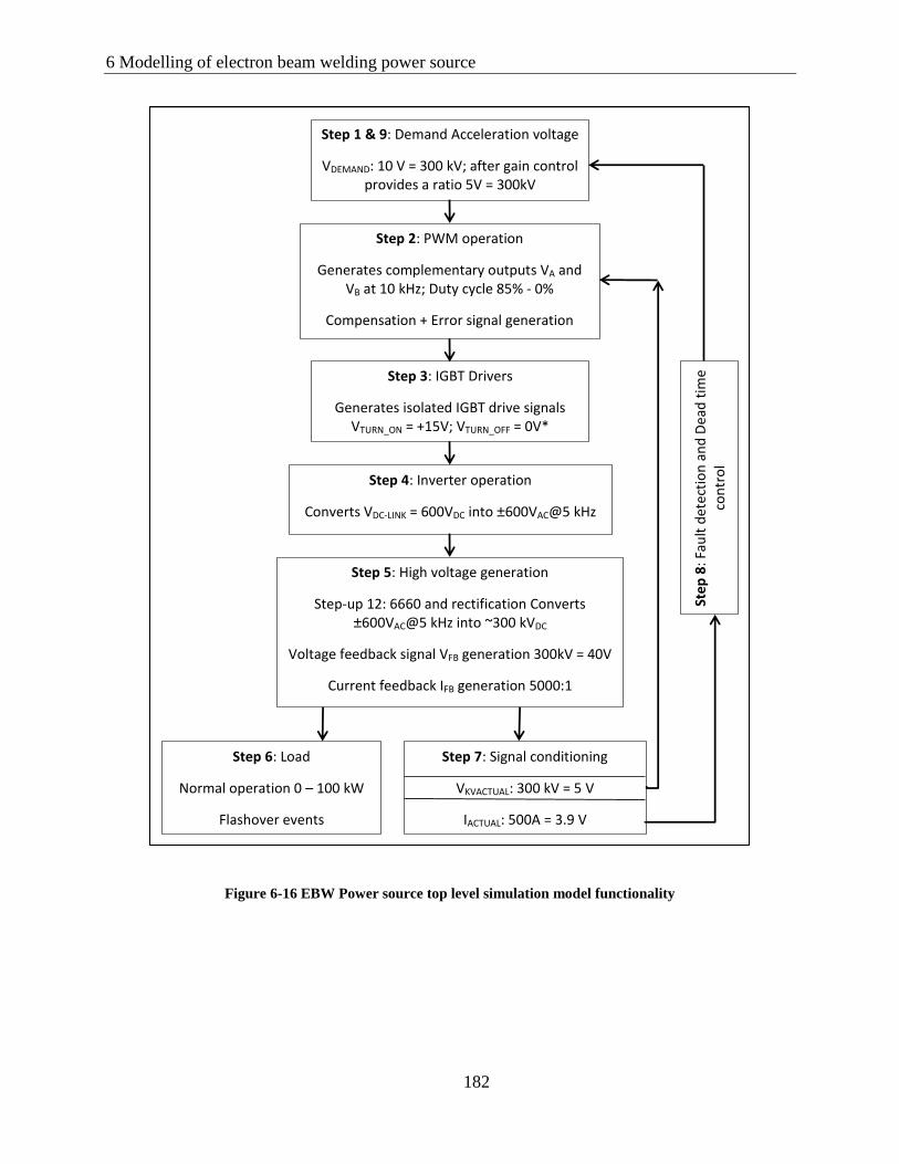
6 Modelling of electron beam welding power source
182
Figure 6-16 EBW Power source top level simulation model functionality
Step 1 & 9: Demand Acceleration voltage
VDEMAND: 10 V = 300 kV; after gain control provides a ratio 5V = 300kV
Step 2: PWM operation
Generates complementary outputs VA and VB at 10 kHz; Duty cycle 85% - 0%
Compensation + Error signal generation
Step 3: IGBT Drivers
Generates isolated IGBT drive signals VTURN_ON = +15V; VTURN_OFF = 0V*
Step 4: Inverter operation
Converts VDC-LINK = 600VDC into ±600VAC@5 kHz
Step 5: High voltage generation
Step-up 12: 6660 and rectification Converts ±600VAC@5 kHz into ~300 kVDC
Voltage feedback signal VFB generation 300kV = 40V
Current feedback IFB generation 5000:1
Step 6: Load
Normal operation 0 – 100 kW
Flashover events
Step
8: F
ault
det
ecti
on
an
d D
ead
tim
e
con
tro
l
Step 7: Signal conditioning
VKVACTUAL: 300 kV = 5 V
IACTUAL: 500A = 3.9 V

6 Modelling of electron beam welding power source
183
Figure 6-17 Simulation showing a typical flashover free 150 kV; 600 mA power delivery
Transient simulation of the completed system model for the power source, showing a
typical flashover free operation, is presented in Figure 6-17. The system model was simulated for
the simulation conditions; VKVOUT = -150 kV; IEBW_Gun = -660 mA with a ramp up time 500 ms,
starting from 10 ms. The power source voltage output VKVOUT, ramps up initially, and charges
beyond the demanded 150 kV. This is shown in Figure 6-17; B1. This is because of the system’s
settling time. In a previous section 6.3.1, the theoretical settling time was discussed as
approximately 10 ms. In this particular simulation, the settling time is much longer at 60 ms for
the following reasons; as the power source is not loaded, i.e., no load current (IEBW_Gun) is
demanded until t = 10 ms as can be seen in Figure 6-17; B2, the output stage is charged to its
maximum (~300 kV) in the short duration of less than 2 ms. Note that the inverter stopped
switching at this stage, stopped delivering current (Figure 6-17; M1 - ICHOKE1) and voltage

6 Modelling of electron beam welding power source
184
(Figure 6-17; M2 – VIN+,IN-). Inverter switching resumed as significant power from the power
source is demanded when delivering 660 mA at a regulated 150 kV.
Figure 6-18 Inverter current for light and heavy load
Observation and lessons that can be learnt from this set of simulation results are
significant as listed below:
The primary current to the high voltage transformer is the inverter output current, ICHOKE1.
For delivering 660 mA load current- IEBW_Gun, ICHOKE1 is as high as 500A implying the
primary resistance at transformer saturation can be as low as 1.2 Ω (600V / 500 A). This is
collectively the parasitic primary resistance and the reflected impedance from the secondary
side of the transformer. In this particular simulation the primary parasitic impedance was set

6 Modelling of electron beam welding power source
185
to 0.7 Ω using an ideal resistor model. At light load, ICHOKE1 can be as low as 200 A. This is
highlighted in Figure 6-18; B1 and T1, respectively.
The figure also shows the slow response of the compensation circuit, revealing even that 150
kV is reached at 0.8 ms (encircled where VKVACTUAL crosses VDEMANDIN) the error signal does
not start to respond until 2.2 ms when it starts ramping down slowly.
It also can be noticed that the shark-fin shape of I(CHOKE1), exposes two different time
constants, highlighting the saturation effect.
6.6.1 Output ripple analysis
Figure 6-19 Acceleration voltage VKVOUT ripple explained (Note: Not drawn to scale)
The acceptable ripple on output voltage VKVOUT and current delivered to the load
IEBW_GUN are 2% (peak-to-peak) and 5% (peak-to-peak) respectively according to the British
standards for EBW machines (BS EN ISO 14744-1 2008). However precision welding
: Inverter output : Output capacitor charging/discharging
: Discharging due to load current : Output voltage
V i_3 V i_1
V o_1 V o_2
V i_2 V i_4
t 1 t 2 t 3 t 4
V d _1
V d _2 V d _1 i V d _2 i
V i_5

6 Modelling of electron beam welding power source
186
applications prefer a much lower ripple. The ripple seen on a typical 150 kV; 660 mA
simulations are included in Figure 6-17; T1 and T2, for VKVOUT and IEBW_Gun respectively. A
voltage ripple as high as 1.3 % (100 × (151 𝑘𝑉 − 149 𝑘𝑉) 150 𝑘𝑉)⁄ has been observed. The
current ripple noticed was insignificant, as the beam current is independent of the high voltage
level in the thermally limited case. Justification for the voltage ripple can be addressed by a
theoretical method, as discussed below with the aid of Figure 6-19.
The EBW power source, has a 4 nF capacitor at its output as a smoothing/ reservoir
capacitor. The 10 metre high voltage cable that connects the anode of the EBW-Gun to the
power source output has a cable capacitance of value 100 pF/m, making the total effective
capacitance at the output of the power source 5 nF. Based on providing 150 kV as VKVOUT and
drawing 660 mA as load current IEBW_Gun, the expected ripple on VKVOUT can be calculated as
follows:
The charging characteristics of the output capacitor are given by Equation 6-6.
Parameters VC, VF, Vi, and Τ are the capacitor voltage after charge time t, the final value
of voltage, the instantaneous initial value of voltage of the capacitor, and the time
constant respectively. The time constant Τ is the product of the equivalent output
capacitance (COUT) and the load resistance (ROUT). Measuring the value of ROUT is
complex and for this calculation ROUT is assumed to be 227 kΩ (VKVOUT/IEBW_Gun).
Parameter t is the charging time. Assuming the switching duty cycle is at its optimum
85%, the charging time of the capacitor is approximately 85 μs. This is indicated as t1 and
t3 in Figure 6-19. Labels t2 and t4 are the dead time during which the capacitors do not get
further charged.

6 Modelling of electron beam welding power source
187
𝐕𝐜 = 𝐕𝐅 + (𝐕𝐢 − 𝐕𝐅)𝐞−𝐭𝚻
Equation 6-6
𝐕𝐝𝐢𝐬𝐜𝐡𝐚𝐫𝐠𝐞 = 𝐈𝐄𝐁𝐖_𝐆𝐮𝐧 × 𝐭 𝐂⁄ Equation 6-7
Voltage Process Formula Calculated Value
Vi_1 -150 kV
Vi_2 Charging = −333 𝑘𝑉 + (−150 𝑘𝑉 + 333 𝑘𝑉)
× 𝑒−85𝜇𝑠 1.135𝑚𝑠⁄
-163.204 kV
Vd_1i Discharging = 660 𝑚𝐴 × 85 𝜇𝑠 5 𝑛𝐹⁄ -11.220 kV
Vo_1 = 𝑉𝑖_2 − 𝑉𝑑_1𝑖 -151.984 kV
Vd_1 Discharging = 660 𝑚𝐴 × 15 𝜇𝑠 5 𝑛𝐹⁄ -1.980 kV
Vi_3 = 𝑉𝑜_1 − 𝑉𝑑_1 150.004 kV
Vi_4 Charging = −333 𝑘𝑉 + (−150 𝑘𝑉 + 333 𝑘𝑉)
× 𝑒−85𝜇𝑠 1.135𝑚𝑠⁄
-163.204 kV
Vd_2i Discharging = 660 𝑚𝐴 × 85 𝜇𝑠 5 𝑛𝐹⁄ -11.220 kV
Vo_2 = 𝑉𝑖_2 − 𝑉𝑑_1𝑖 -151.984 kV
Vd_2 Discharging = 660 𝑚𝐴 × 15 𝜇𝑠 5 𝑛𝐹⁄ -1.980 kV
Vi_5 = 𝑉𝑜_1 − 𝑉𝑑_1 150.004 kV
Table 6-4 Output voltage ripple calculation
The lable Vi_1 is the value of Vi at the start of time t1 and it is assumed to be 150 kV
indicating the demanded VKVOUT is reached. VF is the final value to be reached and it is
calculated as 333 kV. This calculation is based on the high voltage transformer ratio of
12:6660, stepping up the inverter output VAB of value ± 600V. Voltage drops across the
rectifiers are ignored for simplicity. Using Equation 6-6, the charging values of the output
capacitor can be approximately calculated. The discharging is assumed, due to the load
current IEBW_Gun, to occur for the time period 100 μs (switching time 85 μs and dead-time
15 μs) only for simplicity. The voltage drop due to discharging is calculated using
Equation 6-7. Value C is the output capacitance 5 nF. The calculated values for the

6 Modelling of electron beam welding power source
188
labelled points are presented in Table 6-4. The rows highlighted form the trend of the
output voltage, VKVOUT, which has a ripple of approximately 2 kV.
6.6.2 Fault detection and recovery
The system model of the power source includes the fault detection and fault recovery
control circuits. Their operation is discussed in section 6.3.2. In essence the monitored AC
inverter current ICHOKE1 is precision rectified and compared with the overcurrent threshold level,
typically 600A. The resultant signal, referred to as VHTDEADSET, limits the output voltage VKVOUT
to 0V if the protection limit is reached for more than 10 cycles (typically, over 1 ms duration).
Simulation results obtained showed a rectified value of 3.89V for ICHOKE1 = 498 A (almost equal
to 3.9 V = 500 A) in Figure 6-20; (VC5:2) as expected. The precision rectifier circuit implemented
in the design allowed this accurate measurement. In this simulation the protection level is set to ~
650A by setting the threshold to ~ 5.1 V as shown in Figure 6-20; VR3:2 as set in the real
hardware. This simulation results closely matched the design calculation, proving the fitness of
the equivalent circuit model developed for the current transformer (current shunt) and the
accurate performance of the topology specific models used to represent the overcurrent detection
circuits.
The complete operation of fault detection and recovery was simulated with the default 30
ms Weld Dead Time, after flashover detection. The simulation results are presented in Figure
6-21 and are used as an aid to discuss circuit operation. The power stage output was short
circuited at simulation time 2 ms to emulate the flashover fault condition. A simple variable
resistor model, modelled using a control source G in the PSpice ABM library was used to
simulate this condition. The power stage output was connected to ground via this model resistor
and its value was controlled using a pulse voltage source with pulse profile: Initial value = 75

6 Modelling of electron beam welding power source
189
MΩ; time delay = 2 ms; final value = 20 kΩ; fall time = rise time = 1 ms; and pulse width = 2
ms. This allowed simulating a leakage current of 2 mA @ 150 kV which is experienced in real
hardware and a flashover current of ~13 A for 2 ms with a rise and fall time of 1 ms at a
simulation time of 2 ms. A flashover current of 13 A is an arbitrary high current value that
demands very high current from the inverter, making the transformer saturate and causing an
overcurrent situation.
Figure 6-20 Conversion of inverter output current into DC for overcurrent detection (simulation)
On detection of flashover, an error flag VHTDEADSET is generated, which consequently
forces the VDEMANDIN to 0V, which in turn makes the acceleration voltage VKVOUT 0 V. This
operation maintains the VDEMAND at 0 volts for 23 ms. This time is set in the hardware using a
fixed RC network. At the end of 23 ms, the VDEMAND is resumed back to its original setting, 2.5
V in this particular simulation, demanding 150 kV output. The ramp up time is ~ 7 ms set by the
hardware at present. As can be seen the VKVOUT resumed back to 150 kV with minimal overshoot
(compared to the initial stage) just after the VDEMAND recovery.
Traces included in Figure 6-21; M1, highlight the VCE voltage across the IGBTs. This is
of interest to see if the VCE overshoots above the IGBT breakdown voltage of 1200 V during

6 Modelling of electron beam welding power source
190
recovery. At recovery, the IGBTs go under a hard-switching operation switching approximately
600 A at 600 V and maximum duty cycle of 85%. Simulation reveals safe operation is
maintained during the recovery operation, as the VCE is kept below 800 V.
Figure 6-21 Simulation showing flashover detection and VKVOUT recovery in 30 ms
6.6.3 Evaluation of system level operation
Real hardware measurements at a component level suffered because of the system
complexity and limited resources. So the evaluation of all the developed independent component
models was impossible. Efforts had been made to obtain inverter related measurements at a
system level. This is because as aforementioned the EBW systems functionality heavily depends
on the inverter operation and the control circuits implemented in effect controls the switching of
the inverter. Hence a compromise had been made, to agree the simulation model is acceptable, if
the inverter simulation results closely map the real hardware measurements. As an additional

6 Modelling of electron beam welding power source
191
measure to maintain the validity of the model, all important control electronics subsystems were
modelled using topology specific models. Topology specific models are considered to be
accurate and they closely map real hardware.
a
b
c
d
Time
37.3ms 37.4ms 37.5ms 37.6ms 37.7ms 37.8ms
V(INV+,INV-)
0V
-1.0KV
1.0KVB
1
SEL>>
V(DC_LINK,INV-) I(CHOKE1)
-1.0K
0
1.0KT
1
Time
700us 750us679us 792us
1 V(INV+,INV-) 2 -I(CHOKE1)
-0.5KV
0V
0.5KV
1.0KVB
1
SEL>>
-1.0KA
0A
1.0KAB
2
SEL>>
V(DC_LINK,INV-)
0V
0.5KV
1.0KVT
1
Figure 6-22 Inverter performance: figures a and c show the measurement on real inverter hardware
depicting inverter output +/-610V and one of the IGBTs switching 300A and 600 A respectively. Figures b
and d shows the corresponding waveforms in simulation for 300 A an 600 A respectively.

6 Modelling of electron beam welding power source
192
Modelling and evaluation of the power switching device IGBT - DIM800DDM12-A000
utilised in the inverter design is presented in section 6.2.2. These devices experience high 𝑑𝑖/
𝑑𝑡 when used in inverter applications. As a consequence, the IGBTs experience a high voltage
stress as discussed previously due to the presence of parasitic inductance. Keeping the VCE of
IGBTs below their breakdown voltage (VBR) is paramount and the FWDs integrated in the CO-
PACK protects against VBR violation when the devices switch off. The operation of the inverter
was simulated, and compared with the measurements for validation.
Figure 6-22 presents the behaviour of the inverter at two different duty-cycles. Figure
6-22; a, shows a 25μs turn on of IGBTs. Commutation of the load current (CH3) of value 300A
and turning it off at high 𝑑𝑖/𝑑𝑡 is highlighted. The VCE across one of the IGBT approaching ~
800 V was noticed (CH1) during turnoff. Note that 𝑉𝐶𝐸 = 𝑉𝐷𝐶_𝐿𝐼𝑁𝐾 + 𝑉𝑆𝑃𝐼𝐾𝐸. The DC_Link
voltage VDC_LINK was measured as 610 VDC, and varies depending upon the supplied 3 phase
voltage by up to 16%. The inverter output swinging between +600VDC and -600VDC is also
shown (CH4). This is a typical operation of the inverter delivering ~ 20 kW power to load (150
kV@150 mA). The same scenario was simulated and the corresponding results are presented in
Figure 6-22; b. The load current, VCE and the inverter output are named as ICHOKE1, VDC_LINK,INV-
and VINV+,INV- respectively. Close mapping of the simulation results to the real hardware was
observed. Similarly measurements obtained for 600A load current commutation, and the
simulation results obtained for 600 A are presented in Figure 6-22; c and d, respectively. In both
cases the turn-on time was 75 μs.

6 Modelling of electron beam welding power source
193
6.7 Applications
The close mapping of the simulation results to the real hardware measurements and
theoretical calculations validated the use of the system model, which could then be used for
finding optimised parameters, to improve system functionality. Two such applications that
require attention are discussed.
6.7.1 System stability
An exercise has been conducted to see the overshoot behaviour of the output voltage
VKVOUT, for a different configuration of the compensation circuit discussed in section 6.3.1. As
stated, the overshoot behaviour (which is the weighting of the transient response) can be tuned
by adjusting the zeros of the transfer function.
Figure 6-23 Stability of the system
The zeros of the transfer function T(S) of this system can be adjusted by changing the
value of C2 in the compensation network, without compromising the settling time. Simulation
was carried for analysing the effect of tuning the weighting of the transfer function by
-300,000
-250,000
-200,000
-150,000
-100,000
-50,000
0
50,000
0.000 0.005 0.010 0.015
KV
OU
T vo
ltag
e, V
KV
OU
T -(
V)
Time, t - (s)
(a) VKVOUT Settling time and overshoot
enhancement
V(KVOUT) - 150nF V(KVOUT) - 220nF V(KVOUT) - 100nF
V(KVOUT) - 50nF V(KVOUT) - 10nF
-210,000
-200,000
-190,000
-180,000
-170,000
-160,000
-150,000
-140,000
-130,000
0.000 0.005 0.010 0.015
KV
OU
T vo
ltag
e, V
KV
OU
T -(
V)
Time, t - (s)
(b) VKVOUT Overshoot enhancement for optimum
weighting - Zoomed
V(KVOUT) - 50nF V(KVOUT) - 10nF

6 Modelling of electron beam welding power source
194
parameterising the capacitor value C2, ranging from 10 nF to 220 nF. These transient simulation
results are presented in Figure 6-23; a, for varying C2 values. It shows the transient behaviour of
VKVOUT during the initial start-up at which a 150 kV is demanded as a step. VKVOUT stabilised to
its final value of 150 kV for all the simulations, with the smallest overshoot for a C2 value of 10
nF. The maximum overshoot was obtained for a C2 value of 220 nF. Note that the real hardware
is fitted with 220 nF for C2. The transient response time did not change due to this change in
weighting. Figure 6-23; b, is a zoomed version of Figure 6-23; a, highlighting the transient
behaviour of the system for C2 values 50 nF and 10 nF, which also require about 10 ms to settle
down.
The advantage of using modelling to simulate the response of the power supply to
changes in the feedback system operation is that the risk of damage – caused by overvoltage and
high voltage breakdown in the transformer or other HV components is avoided. Instability in HV
feedback loops poses a high risk to expensive, bespoke made HV components. Where experience
exists (from the commissioning stage of power supply development) there is a good correlation
between practical results and the model.
The theoretical analysis, in section 6.3.1 on system stability, concluded the response time,
can be as high as 10 ms which is reflected in the system level simulation.
6.7.2 System modelling fault recovery control circuit enhancement
Enhancement of the control circuit that protects the IGBTs in the inverter against
overcurrent, when large current transients or excursions occur as happens during micro-
discharges and flashover, is crucial for long lasting operation of the system and defect free
welding. Reduction in the duration of the weld dead time after flashover has been identified as a

6 Modelling of electron beam welding power source
195
parameter that requires optimisation. This is because it was revealed in the literature study
(section 5.3.5) that the weld dead time period of 30 ms, set in the hardware is well above the
operational constraints. The weld dead time includes 23 ms of 0V VDEMAND time (TDEADTIME) and
7 ms of VDEMAND recovery time (TRESUME). The time TDEADTIME as discussed in section 5.3.5
relies on the physical properties of vacuum integrity recovery. Shortening of this time relies on a
knowledge of arc quenching and vacuum recovery, which is unknown at present. However, the
time TRESUME can be shortened if the power system and its control circuits can handle the rapid
recovery.
Exercising this in the real hardware would carry a high risk for the inverter IGBT
components and associated electronics, but with the aid of the simulation model this exercise
was carried out for various settings and scenarios. One such exercise is included here, showing
that the TRESUME time is reduced from the default 7 ms to values 5ms, 3 ms, 1 ms and 500 μs.
The response is depicted in Figure 6-24. As can be seen the system resumed to its original weld
setting for all values, but collapses for a TRESUME value of 500 μs. Stress analyses on the
components, especially on the IGBTs, were also carried out. Appendix B includes the results.
Justification for the collapse of the system transient can be analysed with approximations as
follows:
Considering 150 kV; 660 mA power delivery, the inductor current ICHOKE1 flowing
through the high voltage transformer’s primary circuit is approximately 500 A. This is shown in
previous sections. With the turns ratio of 12: 6660, the secondary current flowing through the
smoothing and cable capacitor (4 nF and 1 nF respectively) can be calculated as approximately
0.9A (500 𝐴 × 12 6660⁄ ). Plugging values for a capacitor value C = 5 nF, a charging current I
= 0.9A and a charging time t = (n x 85 μs), where n represents number of cycles in the capacitor

6 Modelling of electron beam welding power source
196
charge Equation 6-8, reveals a value for n ≅ 10. Each cycle in this operation is 100 μs duration,
totalling 1 ms for 10 cycles. This implies, the charging of the output capacitors, to 150 kV
requires a minimum of 1 ms.
7 ms recovery - Pass
5 ms recovery - Pass
3 ms recovery - Pass
1 ms recovery - Pass
500 μs recovery - Fail
Figure 6-24 Fault recovery time optimisation

6 Modelling of electron beam welding power source
197
𝑄 = 𝐶𝑉 = 𝐼𝑡 Equation 6-8
6.8 Summary
An Electron Beam Welding power source was analysed for implementing hardware
changes for performance enhancement. The system modelling approach allowed the system to be
investigated at many levels which was impossible with the real hardware due to its complexity.
The model was constructed from a number of accurate subsystems models designed to derives
theoretical values and manufacturers’ supplied data. There was found to be close mapping of the
simulation and real hardware output results. The simulation results obtained revealed the
possibility of enhancing the HV power supply fault recovery control circuit to provide better
performance during gun flashovers for defect-free welding. It also revealed the possibility of
enhancing the transient behaviour of the system by modifying the system stability and
characterisation circuit. In both cases the status of components or circuits implemented in the
design were not compromised.

198
7 CONCLUSIONS AND RECOMMENDATIONS FOR FURTHER WORK
Design verification of mixed-technology and mixed-signal systems can be difficult and
complex. This research helped advance the assessment procedures to reliably and systematically
assess hardware design changes for two such systems – a LRUT pulser-receiver and a EBW
power source, by means of integrated system modelling. The process addressed the utilisation of
component models with different abstraction levels and simulates them in a computing
environment to answer system and component level questions, verify system performance and
reveal problematic interactions. SPICE based simulation tools were used for modelling and
simulating the model constructs for its inherent ability to support modelling and simulating
electronic circuits.
The research studied the feasibility of enhancing the portability of the pulser receiver in
terms of its size and weight. Portability enhancement by 33% was achieved in terms of size and
weight by downgrading the specification of its primary power source – a battery. The extension
of this work facilitated enhancing the existing pulser receiver hardware to an experiment
enhanced LRUT application of inspecting complex components. The research also critically
analysed EBW power source hardware for obtaining optimum operating parameters that can be
implemented in the hardware for enhancing a weld recovery sequence after major flashover
events. Operating parameters, which shortens the weld recovery sequence by 6 ms had been
identified which is anticipated to improve weld quality. Component values which help improve
the transient overshoot of the acceleration voltage were also derived for enhancing the system
performance.

7 Conclusions and recommendations for further work
199
The motivations for the formalisation of the LRUT subsystem models were manifold,
ranging from proof of concept, validation of hardware specification and design modifications,
verification of the correctness of the design, understanding and communicating the functionality
of the design at a component level as well as at a system level, synthesis of circuits and as a test
platform for maintenance tests. The models facilitated: a feasibility study on the system’s
portability enhancement; verifying new and existing designs, schematic generation and rapid
prototyping of the system’s power supply circuits; and enhancing the hardware to experiment an
enhanced LRUT application. This system is a multi-technology system with integrated mixed-
signal circuits. Combination of top-down and bottom-up methodologies were followed in the
development of the system model for including relevant information and to achieve complete
simulation. The simulation tool LTSpice was utilised for modelling and simulating the system
due to its readily available model library of sensitive components and its ability to accept third
party models. Accurate modelling of mixed signal and digital circuits was not possible with this
tool, but it did not affect the decision making process as alternative methods were used to capture
their performance, and make sure their power consumption data was accounted for in the
decision making.
The models of the EBW power source on the other hand are mixed-signal electronic
circuits and were simulated in PSpice environment. Understanding and communicating the
functionality of the existing design at a component level as well as at a system level was the
main motivation of this work. The integration of the model formulated a complete system model
of the EBW power source and its load that enabled assessing the system’s ability on a fault
handling mechanism for rapid weld recovery after flashover events; and analysis on power-stage
output transient overshoots.

7 Conclusions and recommendations for further work
200
7.1 Discussion on LRUT pulser receiver model
In this work, all relevant subsystems in the pulser-receiver and its load were modelled in
the LTSpice environment and characterised individually for validation, using a combination of
theoretical calculations, measurement data and expert knowledge. Simulation covered the
interaction that some of the subsystems can have when connected together with other subsystems
so that any anomaly can be revealed. The first phase of this work was to compute power
consumption data of the system to reliably specify the power source to the pulser-receiver.
Having the ability of integrating and simulating the load model with the drive circuits for various
load conditions and then using the knowledge gained from their collective performance to derive
the specification for the drive circuits’ power supply allowed the research to determine that the
options for portability was overlooked and that the smaller size HV-Bank would jeopardise the
system performance. The choice of full models used in most simulations allowed precise
prototyping of hardware as well as facilitating new concepts to be tried.
Throughout all the case studies, a model evaluation performed against measurement data
at component level was minimal. Instead, theoretical calculations, expert knowledge in the form
of measurement data from previous hardware obtained in separate work and assumed
subsystems’ specifications were used. This was accepted as adequate, for two major reasons;
first most models used in the development of all power sensitive sub circuits were topology
specific models and were assumed accurate, second the equivalent circuit models developed for
two main components – the battery and the transducer, which influenced the most in the decision
making, were validated against measurement data. The acceptance of accuracy of equivalent
circuit models of 20% and the attention paid in achieving agreement to measurement data only

7 Conclusions and recommendations for further work
201
within the application range satisfied the immediate research need, however this limits these
models’ ability for future adaption or enhancement of hardware.
While simultaneously simulating the complete system was encouraged at early stages in
this research work to capture all inter-coupling nature between subsystems, it was not performed
in the final model or in producing data to compute the overall power performance of the system.
This simplification was considered acceptable, provided that the subsystems whose functionality
affects the battery behaviour and the power consumption differently when connected to one or
more subsystems are simulated together and accounted for in the power budget. This allows
capturing change in power consumption due to the inter-coupling nature between constructs
while help minimising complexity and improve simulation time.
Despite the model performance, in providing a platform, where various functionalities
and design ideas can be assessed, extension of this work had been identified to make better use
of this work in future. They are listed below as recommendations for further work:
1. Discrepancy between the measurement data and the simulation data of 20% for the
transducer elements within the application range is acceptable. This is because; this
discrepancy is also expected in reality between two different elements, because of the
manufacturing procedures. However, agreement within 20% within the application
range, though it satisfies the immediate need, limits the model’s ability to support
further enhancement of hardware. Moreover the model developed required
refinements/ minor adjustments to the data produced by the approximated equations
used to obtain model specific parameters. A review on this process to make the
approximated equations, closer to reality would help advance the ability of the model.

7 Conclusions and recommendations for further work
202
2. It is beneficial if a platform/technology free template is provided for automating
power budgeting purposes. In spite of the reliable computation of the power budget
demonstrated, the individual simulation of model constructs and compiling the data
separately is not ideal when assessment of a new configuration is carried out by a
non-expert. Hence an adequate script or template with a built-in calculation-engine is
needed, so that the power budget for this instrumentation can be automated for
various configurations. A Microsoft Excel worksheet, built-in with a relevant engine
is recommended to fulfil this. The data produced using simulation, can be formulated
using curve-fitting methods, and the resultant equations can be used for building the
engine behind the template.
7.2 Functional analysis of EBW power source
Derivation of optimum operating parameters for the enhanced EBW application was the
main objective of this part of the research. This work introduced an application specific fault
condition – flashover in an EBW application and critically analysed ways of enhancing the
existing EBW power source hardware so that this fault condition can be handled better.
Possibility of shortening the 30 ms weld dead-time, imposed by the fault handling circuits at
detection of flashover to prevent damages to hardware and weld specimen, was investigated.
Limiting conditions for the enhancement: the physical constraints imposed by the welding
environment – Vacuum integrity with regards to gas behaviour were investigated; and hardware
limitations likely to compromise the enhancement procedure were researched. The gap in the
published research work on gas behaviour in a vacuum prevented making a decision on
enhancing fault handling mechanism on the basis of the vacuum recovery time after flashover.
Assessment of the limitations the hardware is likely to cause were researched using system

7 Conclusions and recommendations for further work
203
modelling techniques. All relevant subsystems in this hardware were modelled separately in a
PSpice environment and characterised individually at a subsystem level for validation and to
make them suitable for non-convergence free system level simulation. The validated subsystems
were then integrated together to formalise the system level model and subsequent system level
simulations.
The anticipated modification to a fault handling mechanism was expected to increase the
stress on the hardware at a component level as well as a system level when the system responds
to a flashover fault condition. For this reason a bottom-up design methodology was used in the
system model development for achieving a near reality model. The multilevel abstractions of the
system model and its ability to converge to cycle-by-cycle simulation made the research to
perform a critical assessment of the system at a system level as well as a component level
flexibly. Expert knowledge together with theoretical calculations and the measurement data
obtained at a system level made it possible to evaluate the models at a system level. Component
level measurements suffered due to a lack of resources and limited access, but did not make an
impact in the decision making process due to the model accuracy maintained in this bottom-up
development of the system model. Relaxation of resolution parameters in the simulation settings
enormously helped achieve a non-convergent free simulation without compromising the quality
of the simulation results. The quality of the data produced was assessed by comparing system
model simulation results, against simulation data produced with a much tighter simulation setting
during the characterisation of subsystem models.
The work not only analysed the EBW power source, but also delivered an accurate model
for an off the shelf power device IGBT – DIM800DDM12-A000 to the knowledge base for
public use (Parthipan et al. 2013). With the use of the developed system model, the research

7 Conclusions and recommendations for further work
204
revealed that the hardware could be modified to enhance the flashover fault handling mechanism
by reducing the weld dead-time to 24 ms from 30 ms without compromising the hardware
performance. But the consequence of this on weld quality and most importantly, whether this
prediction agrees with real hardware tests are yet to be tested. A case study on the settling time
of the power-stage output suggests there is room for improvement to optimise the weighting of
the overshoot which occurs.
Implementation of the parameters derived in the real hardware and assessing the weld
performance is recommended as further work.

205
REFERENCES
AboElFotoh, HMF, Iyengar, SS & Chakrabarty, K 2005, 'Computing reliablity and message
delay for cooperative wireless distributed sensor networks subject to random failures', IEEE
transaction on reliablity, 2005, pp. 145-155.
ADS803, TI 2002, ADS803 datasheet, viewed 14 Oct. 2012,
<http://www.ti.com/lit/ds/symlink/ads803.pdf>.
Ali, E, Abdolhosein, N & Stoyan, BB 2005, 'Uninterruptable power supplies', in Uninterruptable
power supplies and active filters, CRC Press, New York.
Aouzale, N, Chitnalah, A & Jakjoud, H 2009, 'PSpice modelling nonlinearity effects on
ultrasonic waves', International Conference on Microelectronics.
Aouzale, N, Chitnalah, A, Jakjoud, H & Kourtiche, D 2007, 'PSpice modelling Diffraction
Effects in Pulse Echo Ultrasonic System', 14th IEEE International Conference on Electronics,
Circuits and Systems.
Arash, R, Jafar, M, Kaveh, M & Mohammad, A 2008, 'Reliablity consideration for high power
zero-voltage-switching flyback power supply', IEEE 13th Internaltional power electronics
and motion control conference.
Arata, Y 1986, 'Electron and laser beam welding in Japan', Electron and Laser Beam Welding,
Pergamon press, Tokyo.
Arata, Y & Tomie, M 1986, 'Development and Application of a Strong Focusing Electron Beam
Gun With Mulit-Stage Electromagnetic Accelerating Units', in Plasma, Electron and Laser
Beam Technology, American Society for Metals, Ohio, USA.

References
206
Athalye, G 1999, 'Design of pulse width modulation based smart switch controller for
automotive applications', IEEE 18th Digital Avionics System Conference, 1999, pp. 8.C.1-1 -
8.C.1-7.
Avolution 2008, Introducing ABACUS, viewed 27 July 2013,
<http://www.avolution.com.au/products>.
Azar, R, Udrea, F, Ng, WT, Dawson, F, Findlay, W, Waind, P & Amaratunga, G 2004,
'Advanced electro-thermal SPICE modelling of large power IGBTs', IEE proc.-Circuits
Devices Syst., June 2004.
Basso, CP 2008, 'Basic blocks and generic switched models', in P Scott (ed.), Switch-mode
Power Supplies, McGrawHill, New York, USA.
Bello, V 1984, 'Using the SPICE2 CAD package for easy simulation of switching regulators in
both continuous and discontinuous conduction modes', Powercon.
Benini, L, Castelli, G, Macii, A, Macii, E, Poncino, M & Scarsi, R 2000, 'A discrete-time battery
model for high-level power estimation', Proceedings of IEEE Europe conference and
exhibition 2000 on design, automation and test, 2000, pp. 35-39.
Benini, L, Castelli, G, Macii, A, Macii, E, Poncino, M & Scarsi, R 2000, 'A discrete-time battery
model for high-level power estimation', Proceedings of IEEE Europe Conference and
Exhibition 2000 on Design.
Binard, J & Ducrot, A 1986, 'Electron beam welding of thick materials with a 200kW gun', 1st
conference on power beam technology, Brighton.
Bluff, RJ 1998, 'Avionic system modelling', Simulation '98. International Conference on, vol
457, pp. 11-18.

References
207
Brodersen, AJ & Al-Ali, AR 1989, 'Macromodels for digital to analog converters', IEEE
Proceedings. Energy and Information Technologies in the Southeas, vol 3, pp. 1235 - 1238.
BS EN 50324-1 2002, 'Piezoelectric properties of ceramic materials and components'.
BS EN ISO 14744-1 2008, 'British standard: BS EN ISO 14744-1', British standards.
Cadence - PSpice 2012, Cadence PSpice A/D and Advanced Analysis, viewed 26 July 2012,
<http://www.cadence.com/products/orcad/pspice_simulation/pages/default.aspx>.
Cazes, R, Dard, P & Sayegh, G, 'Control of the electric discharge (flash) in electron beam
welding gun'.
Chen, N, Deng, Y, Wu, J & He, X 2011, 'An efficient semi-mathematical model for co-pack
IGBT', Applied Power Electronics Conference and Exposition (APEC), 2011 Twenty-Sixth
Annual IEEE, pp. 1833 - 1837.
Christophe, PB 2008, 'Basic blocks and generic switched models', in Switch-Mode Power
Supplies Spice simulations and Practicaldesigns, McGraw Hill, New York.
Christophe, PB 2008, 'Chapter 1: Introduction to power conversion', in Switch-mode power
supplies; Spice simulations and practical designs, Mc Graw Hill, New York.
Cirrus Logic - Apex 2008, PA90, viewed 07 August 2012, <http://www.apexanalog.com.php53-
23.ord1-1.websitetestlink.com/wp-content/uploads/2012/08/PA90U_N.pdf>.
Cirrus logic 2009, 'Application notes: Driving capacitive loads APEX-AN25', Application notes,
Apex, Cirrus Logic, Cirrus Logic.
Committee, Working group C-5 of the systems protection subcommittee of the IEEE power
system relaying 2000, 'Mathematical models for current, voltage and coupling capacitor
voltage transformer', IEEE transactions on Power Delivery, Jan 2000, pp. 62 - 72.

References
208
Cotorogea, M 1998, 'Using analog behavioral modeling in PSpice for the implementation of
subcircuit-models of power devices ', Power Electronics Congress, 1998. CIEP 98. VI IEEE
International.
Donnelly, JM & Gauen, K 1993, 'New IGBTs and simulation models simplify automotive
ignition system design', Power Electronics Specialists Conference, 1993. PESC '93 Record.,
24th Annual IEEE, 1993, pp. 473-481.
Dynamic-ceramic_Dynallox96 2010, 'Datasheet: Material properties; Dynallox 96', Dynamic
ceramic Ltd, Crewe.
Dynex semiconductor 2009, DIM800DDM12-A000, viewed 28 May 2012,
<http://www.dynexsemi.com/assets/IGBT_Modules/Datasheets/DNX_DIM800DDM12-
A000.pdf>.
Dynex semiconductor 2009, DIM800DDM17-A000, viewed 28 May 2012,
<http://www.dynexsemi.com/assets/IGBT_Modules/Datasheets/DNX_DIM800DDM17-
A000.pdf>.
EBL Piezoelectric precision 2010, EBL Lead Zirconate Titanate Characteristics, viewed 07
August 2012, <http://www.eblproducts.com/leadzirc.html>.
Fritz, D, Nazarenko, OK, Irie, H, Abe, N & Ohmine, M 1998, '40 years of electron beam
welding and material processing', 6th International conference on welding and melting by
electron and laser beams, Toulon.
Gallagher, TJ & Pearmain, AJ 1983, 'Electrical insulating materials: Time lag to breakdown', in
High voltage measurement, Testing and Design, John WIley & Sons, New York.
Gallagher, TJ & Pearmain, AJ 1983, High Voltage Measurement, Testing and Design, John
Wiley & Sons Ltd, Bath, Great Britain.

References
209
Galsworthy, JC & Bird, J 1998, 'The electron beam welding of marine components', 6th
International conference on welding and melting by electron and laser beams, Toulon.
Gharaibeh, Y 2008, 'The Novel use of Long Range Ultrasonic Guided Waves in Complex
Structures', EngD Report, Brunel University, London.
Gharaibeh, Y, Sanderson, R, Mudge, P, Ennaceur, C & Balachandran, W 2010, 'Investigation of
the Behaviour of Selected Ultrasonic Guided Wave Modes to Inspect Rails for Long-Range
Testing and Monitoring', Journal of Rail and Rapid Transit, vol 224, no. 3, pp. 1091 - 1104.
Gold, S 1997, 'A PSPICE Macromodel for Lithium-Ion Batteries', 12th Battery Conference on
Applications and Advances.
Gold, S 1997, 'A PSPICE Macromodel for Lithium-Ion Batteries', 12th Battery Conference on
Applications and Advances.
Golten, J & Verwer, A 1991, 'System time response', in Control system design and simulation,
Mcgraw-Hill, London.
Haig, GA & Stavrou, P 2012, 'Defect detection for aircraft components: An approach using
ultrasonic guided waves and neural networks', NDT2012.
Hanson, RC 1986, 'High energy beam (EB/laser) an overview comparison', 1st International
conference on Power Beam Technologies, Brighton.
Hefner, Jr, AR 1991, 'An investigation of the drive circuit requirements for the power insulated
gate bipolar transistor (IGBT)', IEEE Tranaction on power electronics.
Hefner, Jr, AR 1995, 'Modeling buffer layer IGBT for circuit simulation', IEEE Transaction on
power electronics.
Integrated Silicon Solution Inc 2012, datasheet: IS61WV102416BLL CMOS RAM, viewed 15
Oct. 2012, <http://www.issi.com/pdf/61WV102416ALL.pdf>.

References
210
Jiles D, C, Thoelke J, B & Devine M, K 1992, 'Numerical determination of hysteresis parameters
for modeling of magnetic properties using the theory of ferromagnetic hysteresis', IEEE
transactions on Magnetics, Jan 1992, pp. 27 - 34.
Jo da Silva, J, Wanzeller, G, de Almeida Farias, P & da Rocha Nato, JS 2008, 'Development of
Circuits for Excitation and Reception in Ultrasonic Transducers for Generation of Guided
Waves in Hollow Cylinders for Fouling Detection', IEEE Transactions on Instrumentation
and Measurement.
Jo de Silva, J, Goncalves, WM, de, AFP & de, RNJS 2008, 'Development of Circuits for
Excitation and Reception in Ultrasonic Transducers for Generation of Guided Waves in
Hollow Cylinders for Fouling Detection', IEEE transaction on instrumentation and
measurement, 2008, pp. 1149-1153.
Joakim, K 2002, 'The concept of IGBT modelling and the evaluation of the PSPICE IGBT
model', MSc thesis, Alstom Power, Vaxjo.
John, HC, Andrei, V, Xiao-Chun, G, Peter, L & John, V 1991, 'Nonlinear transformer model for
circuit simulation', IEEE Transaction on computer-Aided Design, 1991.
Johns, P 2012, 'HV transformer: 300kV'.
Jose, L, San, E & Antonio, R 2004, 'Models for piezoelectric transducers used in broadband
ultrasonic applications', in Piezoelectric Transducers and Applications, Springer, New York.
Klemperer, O 1959, 'The electron mass and its relativistic change', in Electron Physics - The
physics of the free electron, Butterworths Scientific publications, London.
Kraus, K, Turkes, P & Sigg, J 1998, 'Physics-based model of power semiconductor devices for
the circuit simulator SPICE', Power Electronics Specialists Conference, 1998. PESC 98
Record. 29th Annual IEEE, May.

References
211
Kroeze, RC & Krein, PT 2008, 'Electrical Battery Model for Use in Dynamic Electric Vehicle
Simulations', IEEE Power electronics specialists conference, 2008, pp. 1336 - 1342.
Kroeze, RC & Krein, PT 2008, 'Electrical Battery Model for Use in Dynamic Electric Vehicle
Simulations', IEEE Power Electronics Specialists Conference.
Kuang, S, Barry, WW & Stephen, JF 2000, 'A review of IGBT models', vol 15, no. 6.
Lauwers, E & Gielen, G 1999, 'A power estimation model for high-speed CMOS A/D
Converters', Proceedings of Europe Conference and Exhibition on Design, Automation and
Test.
Lauwers, E & Gielen, G 2002, 'A power estimation models for analogue circuits for architectural
exploration of integrated systems', IEEE transactions on very large scale integration (VLSI)
systems, 2002, pp. 155-1162.
Lauwers, E & Gielen, G 2002, 'Power Estimation Models for Analogue Circuits for Architectural
Exploration of Integrated Systems', IEEE Transactions on Very Large Scale Integration
(VLSI) Systems, 2002, pp. 155 - 162.
Leach, MW 1994, 'Controlled-Source Analogous Circuits and SPICE Models for Piezoelectric
Transducers', IEEE transaction on ultrasonics, ferroelectrics, and frequency control, Jan
1994.
Linear Technology - LTSpiceIV 2012, Linear Technology - Design simulation and device
models, viewed 26 July 2012, <http://www.linear.com/designtools/software/#LTspice>.
LT3751 2008, Datasheet, viewed 23 September 2012,
<http://cds.linear.com/docs/Datasheet/3751fc.pdf>.
LTSpiceIV 2009, LTSpice user manual, viewed 10 August 2013,
<http://ecee.colorado.edu/~mathys/ecen1400/pdf/scad3.pdf>.

References
212
Luo, J & Jha, NK 2001, 'Battery-Aware Static Scheduling for Distributed Real-Time Embedded
Systems', pp. 444 - 449.
Majed, AM Dec., 1994, 'Power supply for Electron beam welder', ERA Technology - Design
division, Leatherhead.
Ma, CL & Lauritzen, PO 1991, 'A simple power diode model with forward and reverse recovery',
Power Electronics Specialists Conference, 1991. PESC '91 Record., 22nd Annual IEEE, pp.
411 - 415.
Meleka, AH 1971, Electron-Beam Welding: Principles and practice, Mcgraw-Hill, Maidenhead.
Mentor Graphics 2012, SystemVision - Virtual lab for mechatronics system design and analysis,
viewed 26 July 2012,
<http://www.mentor.com/products/sm/system_integration_simulation_analysis/systemvision/
>.
Metzner, D, Schafer, J & Chihao, X 2001, 'Multi domain behavioral models of smart-power ICs
for design integration in automotive applications', Behavioral Modeling and Simulation, 2001.
BMAS 2001. Proceedings of the Fifth IEEE International Workshop on, 2001, pp. 84 - 89.
Michael, VF 1998, 'Galileo-Probe Battery-Life Estimation', Proceedings annual reliablity and
maintainability symposium, 1998.
Microsim Corporation 1997, Circuit Analysis Software ; page 6 - 42, viewed 21 August 2012,
<http://perso.he-arc.ch/gerald.huguenin/PSPICE_users_guide_AD.pdf>.
Middlebrook, RD & Slobodan, C 1976, 'A general unified approach to modelling switching-
converter power stages', IEEE Power Electronics Specialists Conference, Cleveland.
Min, C & Rincon-Mora, GA 2006, 'Accurate Electrical Battery Model Capable of Predicting
Runtime and I-V Performance', IEEE transaction on energy conversion, 2006.

References
213
Mitsubishi Electric 1998, Mitsubishi IGBT Modules CM1000HA-24H, viewed 21 August 2012,
<http://www.datasheetcatalog.org/datasheet/MitsubishiElectricCorporation/mXvszuw.pdf>.
Mitsubishi Electric 1998, Using GIBT Modules, viewed 21 August 2012.
Mizuno, M, Dairaku, M, Ohara, Y, Ozaki, A, Tanaka, S, Uede, T, Watanabe, K, Yamashita, Y &
Yokoyama, K 1989, 'Inverter type high voltage DC power supply for negative-ion-based
neutral beam injectors', Fusion Engineering, 1989. Proceedings., IEEE Thirteenth Symposium
on.
Mohan, N, Robbins & Robbins, WP 1995, Power Electronics: Converters, Applications, and
Design, John Wiley & Sons, New York.
Moreland, J 1998, 'Choosing a simulation Tool', IEE Colloquium - Power Electronics and
Simulation, 1998.
Mudge, P 2006, 'Teletest specifications', Plant Integrity - TWI, Cambridge.
Mudge, P & Catton, P 2006, 'Monitoring of Engineering Assets using Ultrasonic Guided Waves',
Proceeding of the 9th European Conference on Non-Destructive Testing, Berlin.
Mudge, P, Lank, A & Alleyne, D 1994, 'A long range method of detection of corrosion under
insulation in process pipework', The 5th European union hydrocarbons symposium,
Edinburgh.
Neal, B 2010, 'Production test data'.
Nightinggale, KR, Sanderson, A, Punshon, C & Werme, LO 1998, 'Advances in EB technology
for the fabrication and sealing of large scale copper canisters for high level nuclear waste
burial', 6th International conference on welding and melting by electron and laser beams,
Toulon.

References
214
O'neill, GD 1959, 'Electron tubes for low and medium frequencies', in Radio frequency
handbook, Mcgraw Hill, New York.
Orcad Inc. 1999, 'Analog devices: IGBT', in OrCad PSpice A/D Reference guide, Orcad Inc.,
USA.
Panigrahi T, D, Panigrahi, D, Chiasserini, C, Dey, S, Rao, R, Raghunathan, A & Lahiri, K 2001,
'Battery life estimation of mobile embedded systems', IEEE 14th international conference on
VLSI design, 2001, pp. 57 - 63.
Parthipan, T 2010, '24 month report: System modelling of ultrasonic non-destructive testing
instrumentation', Brunel University, London.
Parthipan, T Sept, 2011, 'EngD porgress report: Electronic systems enhancement by system
modelling - 36 month'.
Parthipan T C8117 2010, 'Design specification for C8117 - Custom made HT transformer for
MK4 HTPSU', Billy Parthipan, Plant Integrity Ltd., Cambridge.
Parthipan, T, Nilavalan, R, Balachandran, W & Mudge, P 2011, 'Design and Analysis of an
Ultrasonic NDT Instrumentation Through System Modelling', International Journal for
Modern Engineering, 2011.
Parthipan, T, Ribton, C, Mudge, P, Rajagopal, N & Wamadeva, B 2013, 'Enhancement of High
Voltage Electron Beam Welding Power Supply', IEEE ISIE13 conference, Taipai.
Pedram, M & Wu., Q 1999, 'Design Considerations for Battery-Powered Electronics',
Proceedings of the 36th Design Automation Conference, New Orleans.
Peter, VS & P, AC 1976, 'Microdischarges and Microdischarge Simulation in Uniform-Field
High-Voltage Vacuum Gaps', IEEE Transaction on Electrical Insulation.

References
215
Power integrations 2000, Concept 2SB315A, viewed 20 September 2012, <http://igbt-
driver.com/products/scale-1-plug-and-play-drivers/2sb315a>.
Powerex Inc., Using IGBT modules, viewed 20 May 2012,
<https://www.galco.com/techdoc/prx/cm100dy-24a_app2.pdf>.
PTV05010W 2005, PTV0510W 8-A, 5-V INPUT NONISOLATED WIDE-OUTPUT ADJUST SIP
MODULE, viewed 13 Jan. 2013, <http://www.ti.com/lit/ds/symlink/ptv05010w.pdf>.
Punshon, CS, Sanderson, A & Belloni, A 1998, 'Reduced pressure electron beam welding for
steel pipelines', 6th International conference on welding and melting by electron and laser
beams, Toulon.
Puttmer, A, Hauptmann, P, Lucklum, R, Krause, O & Henning, B 1997, 'SPICE Model for lossy
piezoelectric transducers', vol 44, no. 1, pp. 60 - 66.
Quang, D, Deming, C & Martin, DFW 2010, 'Dynamic power estimation for deep submicron
circuits with process variation', Design Automation Conference (ASP-DAC) 15th Asia and
South Pacific.
Rakhmatov, DN 2005, 'Battery Voltage Prediction for Portable Systems', IEEE International
Symposium on Circuits and Systems.
Rakhmatov, DN & Vrudhula, SBK 2001, 'An Analytical High-Level Battery Model for Use in
Energy Management of Portable Electronic Systems', IEEE/ACM international conference on
computer aided design, 2001, pp. 488 - 493.
Rakhmatov, DN & Vrudhula, SBK 2001, 'An Analytical High-Level Battery Model for Use in
Energy Management of Portable Electronic Systems', IEEE/ACM International Conference
on Computer Aided Design.

References
216
Ramos, A, San Emeterio, JL & Sans, PT 2000, 'Improvement in transient piezoelectric responses
of NDE transceivers using selective damping and tuning networks', IEEE transaction on
Ultrasonics, Ferroelectrics and Frequency control, 2000, pp. 826-835.
Ramy, A, Florin, U, Mahesh, DS, Gehan, A, Wai, TN & Francis, D 2004, 'Advanced SPICE
modeling of large power IGBT modules', vol 40, no. 3.
Ramy, A, Florin, U, Wai, TN, William, F & Peter, W 2008, 'The current sharing optimization of
paralleled IGBTs in a power module tile using PSpice frequency dependent impedance
model', IEEE Transaction on power electronics.
Rao, R, Vrudhula, S & Rakhmatov, DN 2003, 'Battery modeling for energy aware system
design', Computer socity, Dec 2003, pp. 77- 87.
Reinhold, G & Gleyvod, R 1975, 'Megawatt HV DC power supplies', Nuclear science IEEE
Transactions on, 1975.
Reinhold, G & Minkner, R 1965, 'Stabilized DC Power Supplies for Beam Injection into Orbital
Accelerators', Nuclear Science, IEEE Transactions on, vol 12, no. 3, pp. 820-823.
Russell, JD 1981, 'High Power Electron-beam Welding', Aircraft Engineering and Aerospace
Technology, vol 53, no. 11, pp. 21-24.
Ryan, CK & Philip, TK 2008, 'Electrical Battery Model for Use in Dynamic Electric Vehicle
Simulations', IEEE Power electronics specialists conference, 2008, pp. 1336 - 1342.
Sanderson, A 1978, 'Magnetic trap devices for the elemination of high voltage breakdown in
electron-beam welding equipmwnt', 4th International conference on Advances in welding
processes, The welding institute, Harrogate.

References
217
Sanderson, A 1986, 'Recent innovations in high power electron beam equipment design for
industrial welding applications', International conferance on Power beam technology, TWI,
Brighton.
Sanderson, A & Ribton, CN 1998, 'The development of RF excited guns and intelligent power
supplies for EBW at upto 150kW and 300kV', 6th International conference on wleding and
melting by electron and laser beams, Paris.
Sattar, A 2001, Insulated Gate Bipolar Transistor (IGBT) Basics, IXYS Corporation, viewed 27
August 2012, <http://www.ixys.com/Documents/AppNotes/IXYS_IGBT_Basic_I.pdf>.
Schulze, KR & Powers, DE 1998, 'Nonvacuum electron beam welding: Convenient and highly
productive', 6th International conference on welding and melting by electron and laser
beams, Toulon.
Scott, M & Philip, M 2008, Modelling and Experimental Validation of the Acoustic Electric
Feedthrough Technique, DTSO, Victoris, viewed 02 MARCH 2013,
<http://www.dtic.mil/cgi-bin/GetTRDoc?AD=ADA496556>.
Shcherbakov, AV 2012, 'Switching processes in power sources for electron beam welding gas
with formation of high-voltage breakdown', Welding International, vol 26, no. 3, pp. 221-226.
Sherrit, S, Leary, SP, Dolgin, BP & Bar-Cohen, Y 1999, 'Comparison of the Mason and KLM
Equivalent Circuits for Piezoelectric Resonators in the Thickness Mode', Proceedings of IEEE
Ultrasonics Symposium, 1999, pp. 921 - 926.
Shih, F-Y, Chen, Y-T, Chen, DY & Wu, Y-P 1995, 'A PSpice-compatible model of PWM IC for
switching power converters with soft-start characteristic', Power Electronics and Drive
Systems, 1995., Proceedings of 1995 International Conference on, Feb 1995, pp. 335-340.

References
218
Shilpa, S & Taranjit, SK 2003, Convergence guide, viewed 05 June 2013,
<http://www.orcad.com/documents/community.an/pspice/PSpice_Convergence.pdf>.
Signal, C & Somanchi, S 1998, 'Automotive and aerospace circuit fault analysis', 17th IEEE
Digital Avionics Systems Conference, 1998, pp. 116/1-116/7.
Steele, J & Eddlemon, D 1993, 'Use high-voltage op amps to drive power MOSFETs', Electronic
design - Analog Applications.
Svilainis, L & Motiejunas, G 2006, 'Power amplifier for ultrasonic transducer excitation',
Ultragarsas.
Synopsys 2012, Synopsys Saber platform, viewed 26 July 2012,
<http://www.analogy.com/Systems/Saber/Pages/default.aspx>.
Tang, Y 1998, 'MSc Thesis: High power inverter EMI characterization and improvement using
auxiliary resonant snubber inverter', Virginia Politechnic Institute and State University,
Blacksburg.
Thomas, SG, Linda, MT & Arthur, JB 1982, 'A sixteen-bit monolithic bipolar DAC', IEEE
Solids state circuits, vol 17, pp. 1127 - 1132.
Uwe, D, Didier, C, Andreas, M & Jphann, WK, Design Tools for Power Electronics: Trends and
Innovations, viewed 01 Apr. 2013,
<http://www.pes.ee.ethz.ch/uploads/tx_ethpublications/drofenik_APE07_01.pdf>.
Vacuumschmelze 2012, MEGAPERM 40L® Magnetic properties, viewed 12 August 2012,
<http://www.vacuumschmelze.com/index.php?id=334>.
Van Deventer, J, Lofqvist, T & Delsing, J 2000, 'PSpice simulation of ultrasonic systems',
Ultrasonics, Ferroelectrics and Frequency Control, IEEE Transactions on, vol 47, no. 4, pp.
1014 - 1024.

References
219
Vinnikov, D & Laugis, J 2007, 'High voltage Auxiliary Power Supply with the simplified power
circuit topology for the DC trains', Electrical Power Quality and Utilisation, 2007. EPQU
2007. 9th International Conference on.
Vladimirescu, A 1990, 'SPICE - The third decade', IEEE 1990 Bipolar circuits and technology
meeting 5.1.
Vladimirescu, A 1994, 'Convergence advice', in The spice book, John Wiley & Sons, Inc.,
NewYork.
Vladimirescu, A 1994, 'Spice algorithms and options', in The spice book, John Wiley & Sons,
Inc., New York.
Vladimirescu, A 1999, 'SPICE - The forth decade: Analog and mixed-signal simulation - A state
of the art', Semiconductor Conference, 1999. CAS '99 Proceedings. 1999 International.
Wei, A 2007, 'The Expected Energy Efficiency Consumption of Wireless Distributed Sensor
Networks Based on Node Random Failures', Communications and Networking in China -
CHINACOM, China.
Xiaojin, Z, Hao, C, Yong, S & Meiyu, L 2007, 'Design of Piezoelectric Power Amplifier Used
for Adaptive Structural Vibration Control', , Proceedings of 8th International conference on
Electronic Measurement and Instruments.
Xilinx power estimator 2010, Xilinx FPGA power avandtage at every level, viewed 14 Oct 2012,
<http://www.xilinx.com/products/technology/power/index.htm>.
Xilinx Spartan-3A DSP 2011, datasheets, viewed 14 Oct. 2012,
<http://www.xilinx.com/support/documentation/data_sheets/ds705.pdf>.

I
APPENDIX A: MODELLING OF ELECTROMECHANICAL COMPONENTS IN SPICE
This appendix offers a quick review on the procedures followed to model the
electromechanical components described in Chapters 3 and 4. The content of this appendix
provides enough information to support the development of the electromechanical models used
in the LRUT system: piezoelectric transducer element, LRUT transducer and the medium – the
test specimen. Most of this work was based on the published work carried out by (Puttmer et al.
1997), (Scott & Philip 2008) and (Van Deventer, Lofqvist & Delsing 2000) on implementing the
acoustic nature of piezoceramic materials using a lossy transmission line model (LTRA) in
SPICE based simulators. A step-by-step procedure documented in the British standard for
piezoelectric transducers (BS EN 50324-1 2002) for calculating a complete set of material
coefficients of piezoceramics was also used in conjunction with the aforementioned literature to
derive the models.
A 1. Lossy transmission line model
Lossy transmission line models are described using telegraphic equations. The time delay
necessary in piezoceramics for a mechanical signal to travel from one side to the other, together
with its acoustic attenuation can be represented using the transmission line models. The analogy
of this is very well documented in (Van Deventer, Lofqvist & Delsing 2000). This model in
SPICE can be described as below:
.model Name LTRA (len=length R=resistance L=inductance C=capacitance)

Appendix A: Modelling of electromechanical components in SPICE
II
The material data: cross-sectional area A, the density, mechanical quality factor Qm, the
speed of sound in the material Vp and characteristic frequency fp can be used with Equation A- 1,
Equation A- 2 and Equation A- 3 can be used to determine the L, C, R of the LTRA model to
model an acoustic layer of the chosen material. An attenuation constant can also be utilised in the
calculation if attenuation effects required in the modelling. This work did not include this as the
attenuation effect is insignificant in the short length of material considered. The parameter len is
the length (thickness) of the material. This model has been used extensively in this work to
model all the concerned electromechanical components, discussed in the next section.
𝐿 ≡ 𝐴𝜌 Equation A- 1
𝐶 ≡1
𝐴𝜌𝑉𝑝2 Equation A- 2
𝑅 ≡2𝜋𝑓𝑝𝐿
𝑄𝑚 Equation A- 3
A 2. Electromechanical model description
Figure A- 1 Schematic of the LRUT transducer and the test specimen

Appendix A: Modelling of electromechanical components in SPICE
III
Figure A- 1 shows a schematic of the LRUT transducer and the medium (test specimen)
that required modelling. The LRUT transducer is a hybrid of a steel backing mass, piezoelectric
transducer of type EBL#2 (EBL Piezoelectric precision 2010) and a face plate of material Al2O3
(Dynamic-ceramic_Dynallox96 2010). An adhesive is used to glue the EBL#2 piezoelectric
transducer to the steel backing mass and the face plate to the piezoelectric transducer. The
medium is a metal piece that is under LRUT inspection. This case study used an aluminium plate
of size 30 cm x 1 m x 10 mm. A defect of size 1 mm x 1 m x 10 mm was introduced in the
middle of the medium for demonstration purposes.
Figure A- 2 An equivalent circuit model developed in LTSpice
An equivalent circuit model of the schematic shown in Figure A- 1 is depicted in Figure
A- 2. It consists of the equivalent circuit models of the piezoelectric transducer of type EBL#2,
steel backing mass, face plate and the test specimen with a defect on it. The adhesive layers in
the LRUT transducer assembly were not included, but can be included should the information on
it be provided. The following sections describe the step by step procedure followed to model all

Appendix A: Modelling of electromechanical components in SPICE
IV
these components individually and integrating them to form the subsystem level components
LRUT transducer and the medium that can be simulated in LTSpice environment.
A 3. Model development of EBL#2 piezoelectric transducer element
The LRUT transducer is built on a shear mode piezoelectric transducer EBL#2 (EBL
Piezoelectric precision 2010) of dimension 13 mm (length - l) x 10 mm (width – w) x 0.5 mm
(thickness – t). This research modelled this transducer element using the Puttmer model (Puttmer
et al. 1997). Puttmer developed this model for a thickness mode piezoelectric transducer. But it
was used to model this sheer mode transducer because, as (Jose, San & Antonio 2004), argues
the thickness is very much smaller than the other two dimension and the effect on simulation
would be insignificant. This model is included below in Figure A- 3 for completion.
Figure A- 3 Puttmer model (Scott & Philip 2008)
The model has three terminals: Electrical terminal E; Mechanical terminals: Back face B
and front face F. The back face terminal B was used to add the backing mass model and the front
.subckt pzt E B F 01 B 1 F 1 mylossyTlineTrans V1 1 2 E1 2 0 4 0 1 V2 E 3 C0 3 0 c0T F1 0 3 V1 hc0T F2 0 4 V2 hT R1 4 0 1E3 C1 4 0 1 .model mylossyTlineTrans LTRA (LEN=thickT R=RT L=LT C=CT) .ends

Appendix A: Modelling of electromechanical components in SPICE
V
face terminal F was used to connect the face plate model. The model “mylossyTlineTrans” is a
lossy transmission line model (LTSpiceIV 2009) that emulates the piezoceramic material
properties of the EBL#2 transducer during simulation.
The functionality of the piezoelectric transducer is electromechanical and in the Puttmer
model, the LTRA model represents the mechanical nature of the piezoceramic material. In the
electrical section, the element C0 represents the static capacitance (mentioned and measured as
free capacitance CT in Chapter 3) of the component and it can be calculated using Equation A- 4
(Puttmer et al. 1997), (Van Deventer, Lofqvist & Delsing 2000). The clamped elastic modulus
(C55D) can be extracted from the transducer’s datasheet (EBL Piezoelectric precision 2010).
𝑐0𝑇 =𝐶𝑙𝑎𝑚𝑝𝑒𝑑 𝑒𝑙𝑎𝑠𝑡𝑖𝑐 𝑚𝑜𝑑𝑢𝑙𝑢𝑠 × 𝐴𝑟𝑒𝑎
𝑇ℎ𝑖𝑐𝑘𝑛𝑒𝑠𝑠 𝑜𝑓 𝑡ℎ𝑒 𝑚𝑎𝑡𝑒𝑟𝑖𝑎𝑙 Equation A- 4
𝐺𝑎𝑖𝑛𝐹1 = ℎ𝑡𝑐0𝑇 Equation A- 5
ℎ𝑡 =𝑃𝑖𝑒𝑧𝑜𝑒𝑙𝑒𝑐𝑡𝑟𝑖𝑐 𝑠𝑡𝑟𝑒𝑠𝑠 𝑐𝑜𝑛𝑠𝑡𝑎𝑛𝑡 𝑖𝑛 𝑡ℎ𝑒 𝑑𝑖𝑟𝑒𝑐𝑡𝑖𝑜𝑛 𝑜𝑓 𝑝𝑟𝑜𝑝𝑎𝑔𝑎𝑡𝑖𝑜𝑛
𝑝𝑒𝑟𝑚𝑖𝑡𝑖𝑣𝑖𝑡𝑦 𝑜𝑓 𝑓𝑟𝑒𝑒 𝑠𝑝𝑎𝑐𝑒 Equation A- 6
The interaction between the electrical and mechanical domain of the transducer was
implemented using the current-control-current-source F1 and F2 in the Puttmer model as per its
predecessor Leach model (Leach 1994). The gain factor for F1 was determined as a product of
the transmitting constant h of the material and the static capacitance c0T as shown in Equation
A- 5. Gain for F2 was h - the value of the transmitting constant. This value can be determined
using Equation A- 6. The value of permittivity of free space is 8.8542e-12 CV-1
m-1
(Scott &
Philip 2008). Note that the suffix t implies a thickness mode operation and the same notation was
kept as per the literature in this appendix to maintain uniformity.

Appendix A: Modelling of electromechanical components in SPICE
VI
Determination of model parameters
The Puttmer model for EBL#2 piezoelectric transducer required six parameters: c0T, hc0T, hT,
the RT, LT and CT to be inputted (specified within curly brackets) to make this model specific to
EBL#2 piezoelectric element. A set of coefficients of the piezoceramics material properties of
this transducer required determining, to calculate values for these parameters.
EBL#2 piezoelectric transducer data
Parameters Symbol Value Unit
Thickness t 0.0005 m
Width w 0.003 m
Length l 0.013 m
Area A 0.000039 m2
Density ρ 7500 kg/m3
factor pi π 3.141592654
Free capacitance CT
1.1E-09 F
Permittivity of free space e0 8.8542E-12 C/Vm
Series resonant frequency fr 1650000 Hz
Parallel resonant frequency fp 2350000 Hz
Mechanical quality factor Qm 65
Shear coupling factor k15 7.5
Table A- 1 EBL#2 piezoelectric transducer data extracted from (EBL Piezoelectric precision 2010) and
measurement
Table A- 1 lists the measured values: free capacitance CT; characteristic frequencies fr
and fp; and mechanical dimensions of an EBL#2 transducer and some of the extracted values
from its datasheet (EBL Piezoelectric precision 2010). Table A- 2 lists the set of shear mode
specific coefficients of piezoceramic properties that required determining. It also lists their
corresponding approximate equations that allow determining these coefficients by plugging in
the data provided in Table A- 1. The calculated values are the shear mode specific piezoceramic
coefficients specific to EBL#2. British standard for piezoelectric properties of ceramic materials

Appendix A: Modelling of electromechanical components in SPICE
VII
and components (BS EN 50324-1 2002) documents these approximate equations as a step-by-
step procedure for calculating a complete set of material coefficients of piezoceramics. Note that
the piezoelectric coefficients determined were for a shear mode transducer. This is noticeable
from the suffix (X55) used on the coefficients.
Table A- 2 Calculation of piezoelectric material properties of the EBL#2 transducer
Table A- 3 Model parameters for developing Puttmer model for EBL#2 transducer
Having determined the shear mode specific piezoceramic coefficients of EBL#2 all six
parameters required by the Puttmer model to make it specific to EBL#2 can be calculated using
equations A-1 to A-6. Table A- 3 summarise this and shows all six calculated values. Note the
sound velocity (Vp) is referred to as V5D to match the approximation equation given by (BS EN
Piezoelectric property Description Formula number Formula Calculated value SI Unit
k15 Sheer coupling factor Eq 44/ datasheet sqrt((πfr/2fp)*cot(πfr/2fp)) 7.4654E-01
S55D
Elastic compliance coefficient Eq 18 1/4*ρ*fp2t2
2.4144E-11 m2/N
E11T
Piezoelectric stress constant Eq 54 CT*t/A 1.4103E-08 C/m
2
d15 Piezoelectric charge constant Eq 49 k15*(E11T*S55
E) 4.3562E-10 C/N
S55E
Electric compliance coefficient Eq 23 S55D/(1 -k
215) 5.4540E-11 m
2/N
E11S
Piezoelectric stress constant Eq 56 E11T(1-k15
2) 6.2429E-09 C/N
g15 Piezoelectric voltage stress constant Eq 50 d15/E11T
3.0889E-02 Vm/N
C55D
Elastic stiffness constant Eq 20a 1/S55D
4.1419E+10 N/m2
C55E
Elastic stiffness constant Eq 20b 1/S55E
1.8335E+10 N/m2
V5D
sound velocity Eq 36 sqrt(C55D/ρ) 2.3500E+03 m/s
Parameter Description Formula Value Effective Unit
c0T Capacitance E11S*e0*A/t 1.1000E-09 F
ht Transmitting Constant d15/(E11S*e0) 1.6000E+09 Vm2/CF
hc0t Transmitting Constant ht*c0T 1.8700E+00 FV/m
z0T Acoustic Impedance ρ*V5D*A 6.8738E+02 kg/s
LT Lossy TN inductance z0T/V5D
2.9250E-01 kg/m
cT Lossy TN capacitance 1/(V5D*z0T) 6.1907E-07 s2/mkg
rT Lossy TN resistance 2πfr*LT/QT 6.6445E+04 kg/ms

Appendix A: Modelling of electromechanical components in SPICE
VIII
50324-1 2002). Equation numbers given in Table A- 2; column 3, corresponds to the equation
numbers published by (BS EN 50324-1 2002).
The Puttmer model with the above parameters formed an equivalent circuit model for
EBL#2. However, as the equations used were only 1st order approximations the simulation
results produced by simulating this model did not produce results that closely matched the data
provided by the transducer manufacturer EBL. Refinement of values GainF1 and GainF2 were
required to make close mapping of results. The units given in Table A- 3 are effective units
derived from the dimensions of each parameter.
A 4. Modelling of backing mass
The backing mass used in the assembly is a steel block of dimension 13 mm x 10 mm x
10 mm. In the equivalent circuit described in Figure A- 2, it was represented using a simple
resistor of value RSteelBackingMass. This value was calculated using Equation A- 7 (Leach 1994).
The terms used in the equation and their values are presented in Table A- 4. For this simulation a
6 kΩ resistor was used to represent a steel block.
𝑅𝑎𝑐𝑜𝑢𝑠𝑡𝑖𝑐 = 𝜌 × 𝐴 × 𝑉𝑝 Equation A- 7
Steel block of dimension 13 mm x 10 mm x 10 mm
Symbol Description Equation (BS EN 50324-1 2002) Value Unit
ρ Density 7.850E+03 kg/m3
C55D Modulus of elasticity 2.690E+13 Nm
2/kg
Vp Sound velocity sqrt(C55D/ρ) 5.854E+04 m/s
A Area length x width 1.300E+02 mm2
Table A- 4 Material properties used to calculate acoustic impedance of the Steel backing mass

Appendix A: Modelling of electromechanical components in SPICE
IX
A 5. Modelling of face plate
The face plate was also modelled using a lossy transmission line model LTRA. Its model
description is given in Figure A- 2 as a face plate. The characteristic parameters that required
determining (R, L, C) to make the LTRA model specific to an Al2O3 face plate of dimensions 13
mm x 10 mm x 0.5 mm the procedure presented in Table A- 5 was followed. The determined
values for LT, CT and RT tabulated in Table A- 5; column 4, were plugged in the face plate
model during simulation. Validation of this model was not possible due to unavailability of an
electrical terminal on the real face plate for impedance analysis.
Face plate of dimension 13 mm x 10 mm x 0.5 mm
Symbol Description Equation (Scott & Philip 2008) Value Effective Unit
ρ Density 3.670E+03 kg/m3
C55DT
Modulus of elasticity 5.310E+10 Nm2/kg
QT Mechanical q factor 1.000E+03
V5D Sound velocity sqrt(C55
D/ρ) 3.804E+03 m/s
fp parallel resonant frequency V55D/2*t 3.804E+06 Hz
z0T Acoustic impedance*area ρV55DA 1.815E+03 kg/s
LT Lossy transmission line inductance z0T/V55
D 4.771E-01 kg/m
CT Lossy transmission line capacitance 1/z0T*V55
D 1.449E-07 s2/mkg
RT Lossy transmission line resistance 2*π*fp*LT/QT 1.140E+04 kg/ms
Table A- 5 Face plate model parameters calculation, using Al2O3 material properties
A 6. Medium – the test specimen
The medium was also modelled using the lossy transmission line model LTRA. In
Chapter 4, the case study used an aluminium plate of dimensions 0.3 m x 1 m x 10 cm as an
example, where a defect of dimensions 1mm x 1m x 10 cm was introduced. The defect was also

Appendix A: Modelling of electromechanical components in SPICE
X
modelled using the lossy transmission line model. The values of the parameters used in the
model are presented in Table A- 6. It also includes the procedure for determining these values.
Aluminium plate of dimension 0.3 m x 1 m x 0.01 mm
Symbol Description Equation (Scott & Philip 2008) Value Unit
ρ Density 2.770E+03 kg/m3
C55D Modulus of elasticity 7.310E+10 Nm
2/kg
QT Mechanical q factor 1.000E+03
V5D Sound velocity sqrt(C55
D/ρ) 5.137E+03 m/s
fp parallel resonant frequency V55D/2*t 2.569E+05 Hz
z0T Acoustic impedance*area ρV55DA 1.423E+05 kg/s
LT Lossy transmission line inductance z0T/V55D 2.770E+01 kg/m
CT Lossy transmission line capacitance 1/z0T*V55D 1.368E-09 s2/mkg
RT Lossy transmission line resistance 2*π*fp*LT/QT 4.471E+04 kg/ms
Table A- 6 Material properties of the medium and its calculated model specific values
The test specimen had a defect introduced in the middle of it. Hence the equivalent circuit
model was constructed using two separate lossy transmission line models with a third lossy
transmission line model in between them to represent the defect. The model parameters for the
defect model is also included in Figure A- 2, but the procedure is not described in this appendix
as it was similar to the procedure followed for the face plate and medium.
A 7. Integration of models
The models of the piezoelectric transducer, backing mass, face plate and the medium
were integrated together to form an equivalent circuit model of the LRUT transducer and the
medium. This model can be simulated by connecting relevant models of electronic circuits as
discussed in Chapter 4.

I
APPENDIX B: ELECTRON BEAM WELDING POWER SOURCE MODELS
The circuits and component models discussed in Chapters 5 and 6 are provided in this
appendix with a brief introduction to them. All sub circuits other than the power stage (inverter
and the high voltage transformer circuit) and the EBW-Gun were modelled using topology
specific models, meaning all of their models are a direct translation of their schematics. The
power stage and the EBW-Gun were modelled using their corresponding equivalent circuit
models.
The hardware can be configured with different values of components to change their
functionality. Three such functions this research looked at were the kV (acceleration voltage)
recovery time after a flashover fault condition, overcurrent detection in the inverter due to fault
conditions at the load and the power stage output overshoot damping that was discussed in
Chapter 6. This appendix provides the values of the components that set different rates at which
kV recovers after flashover and the values of the component that set different levels of the
overcurrent threshold limit. The procedure for altering the weighting of the power stage
overshoot is discussed in detail in section 6.7.1. The traces showing the effect of changing this
weighting are also presented.
All auxiliary supplies that power up the circuits were modelled using a voltage source
model (VDC) provided in the PSpice: source library and all sensitive nodes and some ideal
interconnections between components or subsystems that triggered non-convergence issues were
introduced with small values of resistors and/ or inductors. This is noticeable in most of the
circuit models included in this appendix.

Appendix B: Electron beam welding power source models
II
B 1. Power stage – The H-Bridge inverter
The inverter was constructed of four IGBTs of manufacturer’s part number
DIM800DDM12-A000 (Dynex semiconductor 2009). This part is a Co-Pack. The PSpice circuit
simulation model developed for the inverter is shown in Figure B- 1.
Figure B- 1 H-Bridge inverter model based on IGBT DIM800DDM12-A000 model
It includes the equivalent circuit models of the IGBTs, free wheel diodes, bulk capacitor
bank and a voltage source. The models of the capacitor bank and the voltage source V2 were
modelled using ideal PSpice models of capacitors in the PSpice: analog library and a pulse
voltage source (VPULSE) in the PSpice: source library respectively. The initial value of the V2
was set to 0 V and was programmed to ramp up in 10 ns to its corresponding value (600 VDC) 10

Appendix B: Electron beam welding power source models
III
ns after a simulation time t = 0 seconds. This helped achieve a non-convergence free simulation.
Other models used in the model development were developed as per their corresponding real
counterparts. In the real hardware the –Ve bus bar is isolated from the GND. But in this
simulation model this node was connected to the GND to provide a reference point. This helps
PSpice to work out the DC operating points which is crucial for transient simulations. This does
not affect the design principle of the inverter in simulation.
a. IGBT model
Figure B- 2 PSpice model for DIM800DDM12-A000
The PSpice model developed for the IGBT of manufacturer’s part number
DIM800DDM12-A000 is depicted in Figure B- 2. This model is based on a Hefner model
(Hefner, Jr 1995). The model parameter description and the values inputted in the model are
listed in Table B- 1. The free wheel diode of this device was modelled separately as shown in
Figure B- 3.

Appendix B: Electron beam welding power source models
IV
Table B- 1 Model parameters for DIM800DDM12-A000 PSpice model
Figure B- 3 PSpice model for the free wheel diode of DIM800DDM12-A000
B 2. Power stage - High voltage transformer and the EBW-Gun
This circuit is the high voltage conversion stage where the output of the inverter (single
phase ±600V at 5 kHz) is converted to 330 kV DC voltage. The circuit model developed for this
subsystem is shown in Figure B- 4. It consists of a number of component models and a brief
description of the main component models are given below:
Parameter Description DIM800DDM1200-A000 Unit
TAU Ambipolar recombination lifetime 3.60E-07 s
KP Internal MOSFET transconductance 63 A/V2
AREA Active area of the device 1.80E-03 m2
BVF Avalanche uniformity factor 2
AGD Gate-Drain overlap area 2.50E-04 m2
WB Metallurgical base width 1.21E-04 m
VT Threshold voltage 5.20E+00 V
KF Internal MOSFET linear region transconductance 4.79E+00 A/V2
CGS Internal MOSFET gate-source capacitance per unit area 1.95E-08 F/cm2
COXD Internal MOSFET gate-drain overlap oxide capacitance per unit area 3.58E-08 F/cm2
VTD Internal MOSFET gate-drain overlap depletion threshold -1.18E+01 V

Appendix B: Electron beam welding power source models
V
Figure B- 4 Models of high voltage transformer arrangement and load
a. Choke
The choke (labelled as choke1) is an air core inductor model. It was modelled using an
ideal inductor.
b. High voltage transformer
The high voltage (HV) transformer was modelled using the Jiles-Atherton model (Jiles D,
Thoelke J & Devine M 1992). The core details were calculated based on the information
provided by the transformer manufacturer (Johns 2012). Parameters inputted in the model are
presented in Table B- 2. The saturation current when the HV transformer saturates was set by the
resistor value R103.
Voltage
divider
Current shunt
arrangement
Saturation
resistance
Rectifier
diodes

Appendix B: Electron beam welding power source models
VI
Table B- 2 HV Transformer core parameters included in the Jiles-Atherton model
c. High voltage rectifier
Figure B- 5 High voltage rectifier diode arrangement
The high voltage rectifier was fabricated by stacking a number of high voltage diodes of
manufacturer’s part number USR100.It is a 10 kV diode. Its model can be found in the PSpice:
DIODE HV library. These are 10 kV diodes. The circuit model developed for the stack of diodes
connected to each arm of the rectifier is shown in Figure B- 5.
Parameter Name Description Value
LENGTH Core path length 224 cm
AREA Cross sectional area 22 cm2
GAP Core gap 0.26e-6
BR Residual flux density 7500 Gauss
BM Saturated flux density 14800 Gauss
HC Coercive magnetic force 0.0753982 Oersted

Appendix B: Electron beam welding power source models
VII
d. High voltage resister network – Voltage divider
The high voltage resister network (Rlower and Rupper) together with the circuit components
built in the kV demand circuit (B 4: b) forms a voltage divider to produce a 40 V DC full-scale
voltage feedback signal when the power stage output is 300 kV, i.e., the scale was set as 300 kV
= 40 V (7500:1). The capacitor divider network connected parallel to this resistor network also
has the same ratio, providing compensation for the unintentionally introduced capacitance
inherited from the high voltage resistors Rlower and Rupper by the transformer arrangement.
e. Load – EBW gun
Figure B- 6 EBW Gun model
The EBW-gun behaviour was modelled using an S-curve equation as shown in Figure B-
6. This model sets the leakage current of the EBW-Gun to 1 mA and the threshold voltage of 60
kV. The temperature control terminal TEMP_CTRL in the model was used to adjust the gain
value of the G-Value (G1) to imitate the thermionic effect of the cathode shown in Figure 6-14.

Appendix B: Electron beam welding power source models
VIII
B 3. IGBT drive circuits
Figure B- 7 IGBT drive circuits
The gate drive circuit (Power integrations 2000) used in the real hardware was not
modelled because the schematics of its circuits were not available. The modelled circuit for the
performing gate drive functionality of this system is shown in Figure B- 7. This circuit matched
the following aspects of the real circuit:
The gate resistor arrangement was formed using a resistor of value 4 Ω in parallel
with a serially connected IN4148 diode and a resistor of value 2Ω (e.g., R112 is
connected in parallel to the serially connected D60 and R111). This was to provide
different turn-on and turn-off time for the IGBTs.

Appendix B: Electron beam welding power source models
IX
Back to back protection diodes were used to emulate protection of the gate of the
IGBTs against gate drive over voltage signals (e.g., Zener diodes D51 and D52 of
manufacturer’s part number BZX84C15). This limits the switching signal level to +/-
15V maximum.
5V logic unipolar PWM output signals (PWM_LEG1 and PWM_LEG2) were level
shifted to +/-15V logic. This functionality was facilitated by the circuit associated
with U45 and U46.
All these features were considered as the main aspects of the IGBT drive circuit required
for matching the real hardware. The functional performance of this circuit model switching two
opposite IGBTs (Figure B- 1:Z3 and Figure B- 1:Z4) is presented in Figure B- 8. The traces
included in it are listed below:
B1: Gate current during turn on and turn off. A difference in the rate of change of
gate charge and discharge current are noticeable.
B2: Switching signals across the gate and emitter of the IGBTs (VGE). Turn-on
voltage and turn-off voltages are +15V and -15V respectively. The minimum dead
time of 20 % between the switching of Z3 and Z4 is also noticeable. This was set
by the parameter dead-time in the PWM model discussed in section 6.3. In the
real hardware it is set by the hardware.
M1: inverter current switches through Z3, showing approximately 900 A
switching through the device.
M2: The VCE across Z3 when the inverter current of value 900 A is switched
through Z3

Appendix B: Electron beam welding power source models
X
T1: inverter current switch through Z4, showing approximately 900 A switching
through the device.
T2: The VCE across Z4 when the inverter current of value 900 A is switched
through Z4
Figure B- 8 IGBT driver circuit functionality of driving IGBTs Z3 and Z4
B 4. Control circuits
The inverter control circuit design mainly includes generation of PWM switching signals,
inverter current monitoring and fault detection circuits necessary for safe operation. The
schematics of the real hardware that perform these functions were translated into topology
specific models. The functionalities implemented in the control circuit model are discussed
below:

Appendix B: Electron beam welding power source models
XI
a. PWM Circuit
The circuit model generates a natural PWM with a built in dead time of 20%. Figure B-
9 is the PSpice circuit model developed to emulate the PWM functionality of the system. The
switching frequency was set to 5 kHz. The feedback loop for the compensation circuit discussed
in section 6.3 was modelled using C69 and R143. The PWM model generates an internal clock
and the ramp signals and sets the dead time.
Figure B- 9 Control circuit model: PWM circuits

Appendix B: Electron beam welding power source models
XII
b. kV demand circuit
Figure B- 10 Control circuit model: a kV demand circuit
This circuit produces a kV demand signal. This circuit also includes features that govern
the weld dead time discussed in section 6.7.2. Its schematic was translated into a topology
specific circuit model as shown in Figure B- 9.
The shortening of the weld dead time discussed in section 6.7.2 is composed of two parts:
the dead time and the ramp time as shown in Figure B- 11.

Appendix B: Electron beam welding power source models
XIII
Figure B- 11 Weld dead time
The modelling of this aspect is discussed below:
Dead time: This parameter is set to approximately 23 ms in the real hardware. This is
facilitated by the circuit formed by components U20B, U31A, U32A, U33, U34, S3
and Q1. The signal HTDEADSET is set when a flashover is detected by the fault
detection circuit discussed in section B 4: 0. When this signal is set, the output of
U31A is pulled down to 0 V. This action subsequently sets the signal Vdemandin to 0 V
by turning on the clamping transistor Q1, which consequently initialises the dead
time. This dead time is reset by the integrating circuit formed by the operational
amplifier circuit formed by U31A. The charging time constant of this circuit is 528 µs
(R94*C54). The U20B - retriggerable monostable multivibrator model of 74HC123,
produces a train of pulses of pulse width 1 µs at a frequency 10 kHz (period 100 µs).
These pulses charge the capacitor C54 to the maximum of 12V (limited by D29), at a
rate of 22.7 mV per pulse. This integrating action subsequently turns off the clamping

Appendix B: Electron beam welding power source models
XIV
transistor Q1, when the voltage across the capacitor C54 - VC54 rises above the set
threshold voltage of the comparator circuit formed by the simulation model U33 of
the voltage comparator LM311. In the existing hardware this threshold value is set to
5V. This implies the charging process requires just over 220 of the aforementioned
pulse to reach this threshold value (5V/22.7 mV). This equates to approximately 23
ms (222.26 cycles x 100 µs = 22.26 ms to be exact). A simulation illustrating this is
shown in Figure B- 12.
Figure B- 12 Simulation showing 23 ms dead time and 7 ms ramp time
The ramp time: In the real hardware this value is set to 7 ms. This parameter is set by
the components C51 and Rramp. The ramp time can be changed by adjusting the value
of the resister Rramp. The values of Rramp for setting different ramp times are given in
Table B- 3.

Appendix B: Electron beam welding power source models
XV
Table B- 3 Ramp time setup
c. kV actual circuit
Figure B- 13 Control circuit model: kV actual circuit
Ramp time Value od C51 Resistor value
7 ms 22 nF 470 kΩ
6 ms 22 nF 395 kΩ
5 ms 22 nF 330 kΩ
4 ms 22 nF 264 kΩ
3 ms 22 nF 198 kΩ
2 ms 22 nF 132 kΩ
1 ms 22 nF 65.9 kΩ
500 us 22 nF 32.9 kΩ
Vkvdivider-
Vkvactual

Appendix B: Electron beam welding power source models
XVI
This circuit signal condition the voltage feedback signal generated at the output of the
power stage by the voltage divider network discussed in B 2: d. Its topology specific circuit
model is shown in Figure B- 13. The output of this circuit model provides a 5V full scale output
signal Vkvactual1 to represent the acceleration voltage of a value 300 kV. This output signal is fed
into the error amplifier built in the PWM model for comparison with the acceleration voltage
demand signal VDemandIn.
d. Inverter current measurement
Figure B- 14 Control circuit model: Inverter current measurement circuit
The control circuit also provides overcurrent detection, with overcurrent shutdown. The
topology specific circuit model for this circuit is presented in Figure B- 14. The inverter current
is sensed by the current shunt depicted in Figure B- 4 at a scale 5000:1 and is fed back into this

Appendix B: Electron beam welding power source models
XVII
circuit. The input stage of this circuit is configured in a way to produce 3.9V at the output of the
operational amplifier circuit formed by U4A when the inverter current is 500A.
Table B- 4 Current limit threshold values
(𝑅𝑥 + 750) =𝑉𝑥 × 10 × 103
(15 − 𝑉𝑥) Equation B- 1
The overcurrent trip is set by the comparator circuit formed by U1A and its associated
resistors R1, RCURRENTLIMIT and R5. Adjusting the value of resistor RCURRENTLIMIT allows
changing the current trip threshold level. Typical overcurrent level settings and their
corresponding threshold voltage values are given in Table B- 4. This table also shows the
corresponding resistor values that can be calculated using Equation B- 1.
e. Fault detection circuit
The circuit models for this circuit are presented in Figure B- 15 and Figure B- 16. These
circuits act upon the detection of an overcurrent situation. When an overcurrent signal is
triggered by the inverter current measurement circuit for ten consecutive switching cycles
(duration of 1 ms) this circuit assert a flashover signal. This time is set by the RC network
formed by the capacitor C10 and the equivalent resistance of value of the parallel combination of
Current setting in A Threshold voltage in V Resistor value of RCURRENTLIMIT in Ω
150 1.17 9.6E+01
200 1.56 4.1E+02
300 2.34 1.1E+03
400 3.12 1.9E+03
450 3.51 2.3E+03
500 3.9 2.8E+03
550 4.29 3.3E+03
600 4.68 3.8E+03
650 5.07 4.4E+03

Appendix B: Electron beam welding power source models
XVIII
R42 and R42 (0.69 x 100 nF x 14.49 Ω). This action subsequently pulls the signal HTDEADSET
high (Figure B- 16) and as a consequence, the weld dead time sequence explained in the kV
demand circuit is initiated.
Figure B- 15 Fault detection circuit model: Flashover detection
An inverter current in excess of 650 A is possible at the initial stage of the kV ramping up
operation. This overcurrent flow is expected to last for more than 10 switching cycles. This
causes the inverter current measurement circuit to assert the overcurrent signal which in a normal
operation leads to a flashover detection signal - flashover to be asserted. To avoid false flashover
triggering during kV recovery this circuit was implemented with a safeguard signal
inhibit_shortflash. This signal prevents retriggering of a flashover signal during the kV recovery

Appendix B: Electron beam welding power source models
XIX
period after flashover, by forcing the signal VTP1 to be kept at a logic level ‘0’ for 4 ms (40
switching cycles) on detection of the first overcurrent signal during kV recovery.
Figure B- 16 Fault detection circuit: Dead time set circuit
