electronic structure. important question: why certain materials are metals and others are...
TRANSCRIPT
Electronic Electronic structurestructure

Important question: Why certain Important question: Why certain materials are metals and others are materials are metals and others are insulators?insulators?
The presence of perfect periodicity The presence of perfect periodicity greatly simplifies the mathematical greatly simplifies the mathematical treatment of the behaviour of electrons treatment of the behaviour of electrons in a solid. The electron states can be in a solid. The electron states can be written as Block waves extending written as Block waves extending throughout the crystal:throughout the crystal:

φφ(k,r) = u(k,r) exp (ikr)(k,r) = u(k,r) exp (ikr)
where where u(k,r)u(k,r) has the periodicity of the has the periodicity of the crystal lattice crystal lattice
u(k,r)=u(k,r+R)u(k,r)=u(k,r+R)
(R is lattice translation vector.),(R is lattice translation vector.),
and term and term exp(ikr) exp(ikr) represents a plane represents a plane wave.wave.

The The allowed wavevectors allowed wavevectors kk of the electrons are related to of the electrons are related to the symmetry ofthe symmetry of lattice. lattice.
Since that a reciprocal lattice Since that a reciprocal lattice related to the unit cell related to the unit cell parameters can be parameters can be established in established in k-spacek-space. .

First Brillouin zone of FCC First Brillouin zone of FCC lattice showing symmetry lattice showing symmetry
labels labels

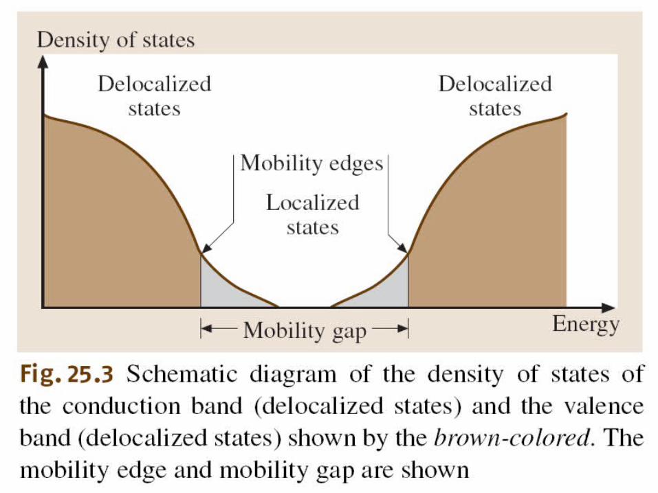
Electron density of states of c-Electron density of states of c-SiSi
Indirect semiconductorIndirect semiconductor
Amorphous materials?Amorphous materials?
There is no periodicity! There is no periodicity! Hence there can be no reciprocal Hence there can be no reciprocal
kk-space. No -space. No kk vector. vector. The electrons can not be The electrons can not be
represented as Block states.represented as Block states.
Should band gap occur in amorphous Should band gap occur in amorphous materials? Yesmaterials? Yes
What is the definition of What is the definition of semiconductors?semiconductors?
1. Conductivity?1. Conductivity? Conductivity is between metals Conductivity is between metals
and insulators?and insulators?2. Gap size? 2. Gap size? It has a gap of 1 – 2 eV?It has a gap of 1 – 2 eV?3. Or?3. Or?

As the temperature of a As the temperature of a semiconductor rises semiconductor rises above above absolute zeroabsolute zero, , there is more energy to there is more energy to spend on spend on lattice vibrationlattice vibration and on and on lifting some lifting some electronselectrons into an energy into an energy states of the states of the conduction conduction bandband. .
Electrons excited to the Electrons excited to the conduction band leave conduction band leave behind behind electron holeselectron holes in in the valence band. the valence band.
Both the conduction band Both the conduction band electrons and the valence electrons and the valence band holes contribute to band holes contribute to electrical conductivity.electrical conductivity.
+
-

Most common definitionMost common definition
The temperature dependence of resistivity The temperature dependence of resistivity at low temperature:at low temperature:
ρρ = = ρρ00 exp( exp(εε00//kB T )
T increasing, ρρ decreasing decreasing
(In metal case:T increasing, ρρ increasing!) increasing!)

Electronic Electronic structurestructure

Covalent bondingCovalent bonding
Amorphous semiconductors are Amorphous semiconductors are typically covalently bonded typically covalently bonded materials.materials.

spsp3 hybrids3 hybrids
Hybridisation describes the bonding atoms Hybridisation describes the bonding atoms from an atom's point of view. A tetrahedrally from an atom's point of view. A tetrahedrally coordinated carbon (e.g., methane, CH4), the coordinated carbon (e.g., methane, CH4), the carbon should have 4 orbitals with the correct carbon should have 4 orbitals with the correct symmetry to bond to the 4 hydrogen atoms. symmetry to bond to the 4 hydrogen atoms.
The problem with the existence of methane is The problem with the existence of methane is now this: carbon's ground-state configuration now this: carbon's ground-state configuration is 1is 1ss2, 22, 2ss2, 22, 2pxpx1, 21, 2pypy11

Ground state orbitals cannot be Ground state orbitals cannot be used for bonding in CH4. While used for bonding in CH4. While exciting 2exciting 2ss electrons into a 2 electrons into a 2pp orbitals would, in theory, allow orbitals would, in theory, allow for four bonds according to the for four bonds according to the valence bond theory, this would valence bond theory, this would imply that the various bonds of imply that the various bonds of CH4 would have differing CH4 would have differing energies due to differing levels of energies due to differing levels of orbital overlap. This has been orbital overlap. This has been experimentally disproved.experimentally disproved.
The solution is a linear combination The solution is a linear combination of the s and p wave functions, known of the s and p wave functions, known as a hybridized orbital. In the case of as a hybridized orbital. In the case of carbon attempting to bond with four carbon attempting to bond with four hydrogens, four orbitals are required. hydrogens, four orbitals are required. Therefore, the 2Therefore, the 2ss orbital "mixes" with orbital "mixes" with the three 2the three 2pp orbitals to form four orbitals to form four spsp3 3 hybridshybrids becomes becomes

spsp3 3 orbitalsorbitals1. sp1. sp33 = = ½ s - ½ p½ s - ½ pxx - ½ p - ½ pyy + ½ p + ½ pzz
2. sp2. sp33 = = ½ s - ½ p½ s - ½ pxx + ½ p + ½ pyy - ½ p - ½ pzz
3. sp3. sp33 = = ½ s + ½ p½ s + ½ pxx - ½ p - ½ pyy - ½ p - ½ pzz
4. sp4. sp33 = = ½ s + ½ p½ s + ½ pxx + ½ p + ½ pyy + ½ p + ½ pzz
Linear Combination of Atomic OrbitalsLinear Combination of Atomic Orbitals
Scalar product:
(n.sp(n.sp33; m.sp; m.sp33) = 0) = 0

spsp33
In CH4, four sp3 hybridised orbitals are overlapped by hydrogen's 1s orbital, yielding four σ (sigma) bonds (that is, four single covalent bonds). The four bonds are of the same length and strength. This theory fits the requirements.
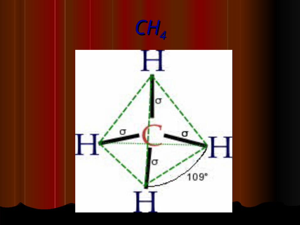
CHCH44
spsp22 hybrids hybrids
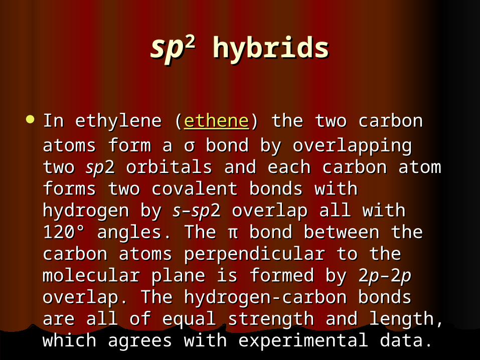
For example, For example, etheneethene (C2H4). Ethene (C2H4). Ethene has a double bond between the has a double bond between the carbons.carbons.
For this molecule, carbon will For this molecule, carbon will spsp2 2 hybridise, because one hybridise, because one π (pi) bondπ (pi) bond is is required for the required for the double bonddouble bond between between the carbons, and only three σ bonds the carbons, and only three σ bonds are formed per carbon atom. In are formed per carbon atom. In spsp2 2 hybridisationhybridisation the 2 the 2ss orbital is mixed orbital is mixed with only two of the three available 2with only two of the three available 2pp orbitals.orbitals.
spsp22 hybrids hybrids
In ethylene (In ethylene (etheneethene) the two carbon atoms ) the two carbon atoms form a σ bond by overlapping two form a σ bond by overlapping two spsp2 2 orbitals and each carbon atom forms two orbitals and each carbon atom forms two covalent bonds with hydrogen by covalent bonds with hydrogen by ss––spsp2 2 overlap all with 120° angles. The π bond overlap all with 120° angles. The π bond between the carbon atoms perpendicular between the carbon atoms perpendicular to the molecular plane is formed by 2to the molecular plane is formed by 2pp–2–2pp overlap. The hydrogen-carbon bonds are overlap. The hydrogen-carbon bonds are all of equal strength and length, which all of equal strength and length, which agrees with experimental data.agrees with experimental data.
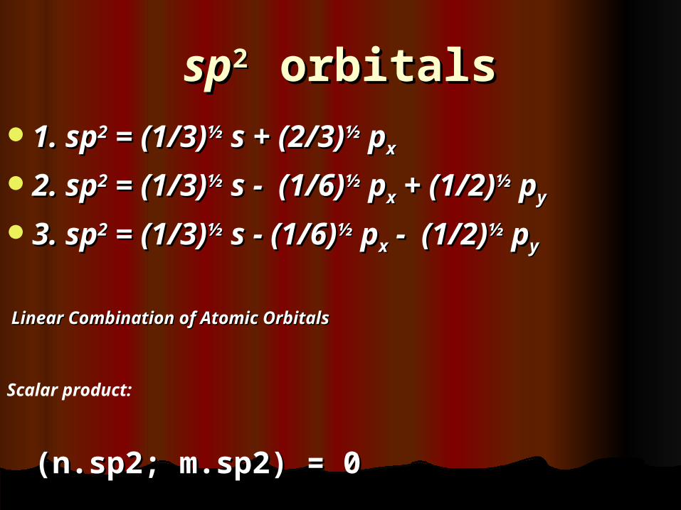
spsp2 2 orbitalsorbitals1. sp1. sp22 = (1/3) = (1/3)½½ s + (2/3) s + (2/3)½½ p pxx
2. sp2. sp22 = (1/3) = (1/3)½½ s - (1/6) s - (1/6)½½ p pxx + (1/2) + (1/2)½½ p pyy
3. sp3. sp22 = (1/3) = (1/3)½½ s - (1/6) s - (1/6)½½ p pxx - (1/2) - (1/2)½½ p pyy
Linear Combination of Atomic OrbitalsLinear Combination of Atomic Orbitals
Scalar product:
(n.sp2; m.sp2) = 0(n.sp2; m.sp2) = 0

spsp22

spsp hybrid hybrid
In C2H2 molecule. Only two sigma In C2H2 molecule. Only two sigma bonds:bonds:
1. sp1. sp33 = (1/2) = (1/2)½½ s - (1/2) s - (1/2)½½ p pxx
2. sp2. sp33 = (1/2) = (1/2)½½ s + (1/2) s + (1/2)½½ppxx

IV. Column materialsIV. Column materials
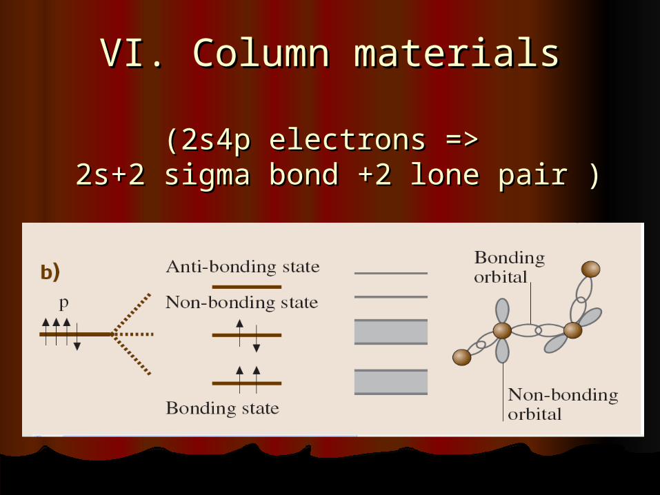
VI. Column materialsVI. Column materials
(2s4p electrons => (2s4p electrons => 2s+2 sigma bond +2 lone pair ) 2s+2 sigma bond +2 lone pair )

Atomic Atomic chargescharges

In crystalline case on monoatomic In crystalline case on monoatomic semiconductors there is no charge semiconductors there is no charge transfer among the same atoms transfer among the same atoms because of translation symmetry.because of translation symmetry.
In non-crystalline case there is In non-crystalline case there is charge transfer because of distorted charge transfer because of distorted sp3 hybridization. sp3 hybridization.
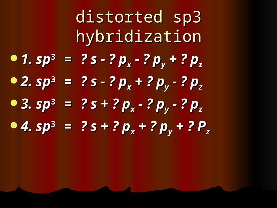
distorted sp3 hybridizationdistorted sp3 hybridization
1. sp1. sp33 = = ? s - ? p? s - ? pxx - ? p - ? pyy + ? p + ? pzz
2. sp2. sp33 = = ? s - ? p? s - ? pxx + ? p + ? pyy - ? p - ? pzz
3. sp3. sp33 = = ? s + ? p? s + ? pxx - ? p - ? pyy - ? p - ? pzz
4. sp4. sp33 = = ? s + ? p? s + ? pxx + ? p + ? pyy + ? P + ? Pzz

Charge accumulation has Charge accumulation has an important influence an important influence on electron energy on electron energy distribution and it plays distribution and it plays an important role for the an important role for the chemical shift in NMR chemical shift in NMR measurementsmeasurements. .

Electronic Electronic density of statesdensity of states
(EDOS)(EDOS)

a-Si RMC I.

Measured structure factor (solid line), Measured structure factor (solid line), RMC model (dashed line)RMC model (dashed line)


Unconstrained model

Constrains for a-SiConstrains for a-Si
Is it really Is it really possible?possible?
Tight Binding Molecular Tight Binding Molecular Dynamics SimulationsDynamics Simulations
We have developed a tight binding We have developed a tight binding molecular dynamics (TB-MD) computer code molecular dynamics (TB-MD) computer code to simulate the real preparation procedure to simulate the real preparation procedure of an amorphous structure, which is grown of an amorphous structure, which is grown by atom-by-atom deposition on a substrate. by atom-by-atom deposition on a substrate. This method differs from most other This method differs from most other molecular dynamics (MD) studies where the molecular dynamics (MD) studies where the amorphous networks are formed by rapid amorphous networks are formed by rapid cooling from the liquid state. Our MD method cooling from the liquid state. Our MD method was successfully used for the description of was successfully used for the description of the amorphous carbon growth.the amorphous carbon growth.
(K. Kohary and S. Kugler, Phys. Rev. B 63 (2001) 193404; and (K. Kohary and S. Kugler, Phys. Rev. B 63 (2001) 193404; and K. Kohary, PhD thesis, Budapest-Marburg (2001), K. Kohary, PhD thesis, Budapest-Marburg (2001), cond-mat/0201312)cond-mat/0201312)
. .

Density of States calculationsDensity of States calculations
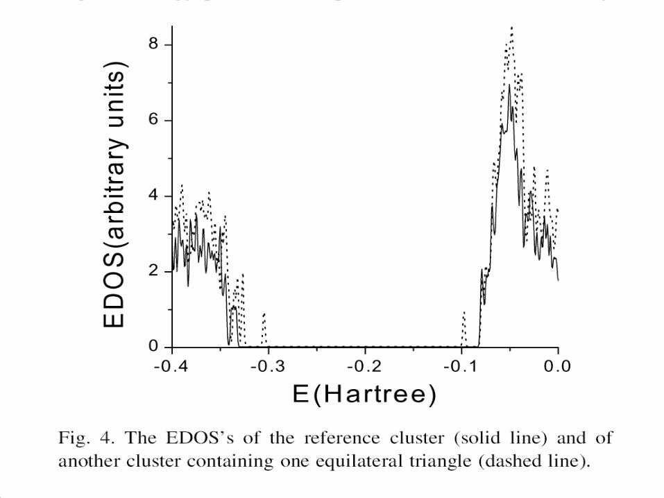
Quantum chemical cluster Quantum chemical cluster calculations at the AM1 level were also calculations at the AM1 level were also carried out in order to find out carried out in order to find out whether the presence of triangles whether the presence of triangles and/or squares cause variations in and/or squares cause variations in terms of the electronic properties.terms of the electronic properties. The electronic density of states (EDOS) The electronic density of states (EDOS) of the WWW model and the modified of the WWW model and the modified WWW models containing triangles and WWW models containing triangles and squares were calculated. squares were calculated.
The reference cluster (a part of The reference cluster (a part of the WWW model) contained about the WWW model) contained about 100 fourfold coordinated Si atoms 100 fourfold coordinated Si atoms and a sufficient number of and a sufficient number of hydrogens saturating the dangling hydrogens saturating the dangling bonds on the boundary of the bonds on the boundary of the cluster. It contains no significant cluster. It contains no significant deviation from a locally nearly deviation from a locally nearly perfect tetrahedral order.perfect tetrahedral order.
First calculationFirst calculation
Based on reference network, we Based on reference network, we constructed other clusters adding constructed other clusters adding silicon (and hydrogen) atoms which silicon (and hydrogen) atoms which formed one, two and three fused or formed one, two and three fused or individual triangles and squares. individual triangles and squares. Significant differences were observed Significant differences were observed in terms of the EDOS: additional in terms of the EDOS: additional higher energy states appeared in the higher energy states appeared in the mobility gap, which are localized on mobility gap, which are localized on the triangle(s) and square(s).the triangle(s) and square(s).

Second calculationSecond calculation
Next figure shows the EDOS Next figure shows the EDOS computed for the central part of the RMC computed for the central part of the RMC structural model obtained at the 10th structural model obtained at the 10th stage, as compared to the EDOS of the stage, as compared to the EDOS of the reference (WWW) cluster. The new reference (WWW) cluster. The new states in the gap correspond to a states in the gap correspond to a bond angle of about 74 deg. in the bond angle of about 74 deg. in the RMC model. Here, it is demonstrated RMC model. Here, it is demonstrated that these states are due exclusively to that these states are due exclusively to bond angles that are smaller than the bond angles that are smaller than the tetrahedral ones. tetrahedral ones.


Journal of Physics: Conference Series 253 (2010) 012013


The endThe end
Optical Optical propertiesproperties

General aspectsGeneral aspects
Optical absorption and Optical absorption and luminescence occur by transition of luminescence occur by transition of electrons and holes between electrons and holes between electronic states (bands, tail states, electronic states (bands, tail states, gap states). If electron-phonon gap states). If electron-phonon coupling is strong enough self-coupling is strong enough self-trapping occurs. trapping occurs.

Absorption coefficient Absorption coefficient αα is defined by is defined by I(z) = II(z) = Ioo exp {- exp {- αα z} z}
where where I(z) I(z) is the flux density if is the flux density if incident light is incident light is IIoo, , z z is the distance is the distance measured from the incident surface. measured from the incident surface. Hence Hence
αα = = - (1/I(z)) dI(z)/dz - (1/I(z)) dI(z)/dz

Absorption Absorption
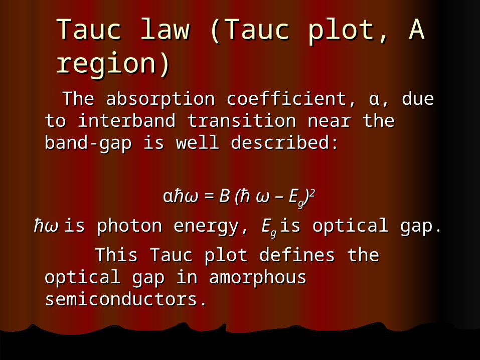
Tauc law (Tauc plot, A region)Tauc law (Tauc plot, A region)
The absorption coefficient, The absorption coefficient, αα, due to , due to interband transition near the band-interband transition near the band-gap is well described:gap is well described:
ααħħωω = B (ħ = B (ħ ωω – E – Egg))2 2
ħħωω is photon energy, is photon energy, EEg g is optical gap.is optical gap.
This Tauc plot defines the optical This Tauc plot defines the optical gap in amorphous semiconductors.gap in amorphous semiconductors.

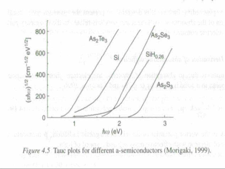
Urbach tail (B region)Urbach tail (B region)
The absorption coefficient at the The absorption coefficient at the photon energy below the optical gap photon energy below the optical gap (tail absorption) depends (tail absorption) depends exponentially on the photon energy:exponentially on the photon energy:
αα((ħħ ωω) ) ~~ exp (ħ exp (ħ ωω/E/Euu)) where where EEuu is called Urbach energy. is called Urbach energy.
C regionC region
In addition, optical absorption by In addition, optical absorption by defects also appears at energy lower defects also appears at energy lower than optical gap. Likewise than optical gap. Likewise αα is written is written as another exponential function of as another exponential function of photon energy:photon energy:
αα((ħħωω) ) ~~ exp (ħ exp (ħωω/E/Edd),),
EEd d belongs to the width of the defect belongs to the width of the defect states. C region is rather sensitive to states. C region is rather sensitive to the structural properties of materials.the structural properties of materials.

PhotoluminescencePhotoluminescence
Photoluminescence occurs as a result Photoluminescence occurs as a result of the transition of electrons and of the transition of electrons and holes from excited states to ground holes from excited states to ground state. state.
After interband excitation, electrons After interband excitation, electrons (holes) relax to the bottom (top) of (holes) relax to the bottom (top) of the conduction (valence) band by the conduction (valence) band by emitting phonons much more quickly emitting phonons much more quickly than the radiative transition.than the radiative transition.

Direct/indirect transitionDirect/indirect transition
In the case of crystalline semiconductors In the case of crystalline semiconductors (without defects, there is no localized (without defects, there is no localized state) photoluminescence occurs by state) photoluminescence occurs by transition between the bottom of the transition between the bottom of the conduction band and the top of the conduction band and the top of the valence band. valence band. kk selection rule must be selection rule must be satisfied: satisfied: kkphotonphoton = k = kii – k – kff . (. (kkphotonphoton, k, kii andand, , kkff are the wave numbers of photons, are the wave numbers of photons, electron of initial and final states.electron of initial and final states.
Since Since kkphotonphoton is much smaller than k is much smaller than kii and and kkff, we can rewrite the selection , we can rewrite the selection rule:rule:
kkii = k = kff..
The semiconductors satisfying this The semiconductors satisfying this condition is called direct-gap condition is called direct-gap semiconductors. c-Si is not satisfying semiconductors. c-Si is not satisfying k-selection rule (indirect-gap k-selection rule (indirect-gap semiconductor). Transition is allowed semiconductor). Transition is allowed by either absorption of phonons or by either absorption of phonons or their emission.their emission.

c-Sic-Si