electronic siulrtiono h ueho dec … types of josephson devices ... 10.3 circuit considerations ......
TRANSCRIPT

R'1D-A12 753 ELECTRONIC SIULRTIONO H UEHOSURFACE MEAPONS CENTER SILVER SPRING HD D JABLONSKIGi DEC 81 NSWC/NP-Si-519 561 RD-F508 877
UNCLASSIFIED F/G 28/iG9 N
EmonEo EIIgEonhohEEEohhhhII-EhhhhEmohhhImhhhEmhhhhhhhIsmhohhhhohmhEmohhshEEEohhhEElhhhEshhEohhE

fl ! ! 128 lI I I I 1. . I .. 1'. 28.,m • , - : -.
= = 332 II111111.0 J&1 -
1.011.2 [UQ41.56.
ILuI
SMICROCOPY RESLUTIN TES CHART
MICROCOPY RESOLUTIN TEST CHART I. NATIONAL BUREAU OF STANOARDS- 1963-A
NATIONAL BUREAU OF STANDARS-963-A
_ .1 NATONL__REUFSNR__93-
II~l,=.o .- I'll' ...._III '
1.21LA 11.
1.25 &64I.4 *L
MICROCOPY RESOLUTION TEST CHARTMICROCOPY RESOLUTION TEST CHART NATIONAL BUREAU O STANARDS-96-A
NATIOANAL BUREAU OF STANDARD-963-AU
h~~h 1.0 Q & '-5 I 3
&W 111 ,,
11.21 LA.1.
~MICROCOPY RESOLUTION TEST CHART
NATIONAL BUREAU OF STANOAROS-1963-Ar
1. LI -1. 1"*~ J&.08 J&.5

NOW MP 81-519 ,....
le LECThRilONIC UM T OFO THlE
BY DANIEL JABLONSKI
RESEARCH AND TECHNOLOGY DEPARTMENT
I DECEMBER 1961
ApevW for t ngm% h ru m in sv wtie mhLw
OCT 20 1982
F: NAVAL SURFACE WEAPONS CENTER
DdthgIin, VWna 22446 S Spring, Malnd 20910
82 i 12 233
" "- -- ".t~i lli.il ll 'III I I I II .1 ...

qECURITY CLASSIICATION OF T1IS PAGE (Whe. naa IDat Xf)
REPORT DOCUMENTATION PAGE X",R COMP LZ oltsSZF]Ol COMdPI,9T =G PORM1. REPORT HUNER L GOVT ACCESSION NO. L RECIPIENT'S CATALOG NUME
Ir NSWC Me 81-519 ________ ____
4. TITLE fnyd Subtftle) S. TYPE oP REPORT a PERIOo COVIRED
ELECTRONIC SIMULATION OF THE JOSEPHSON EFFECTS s. PERFORMING ORG. REPORT UU.ER
7. AUTHONRa) NI OTRACT OR RANT NUNBCAIs)Daniel Jablonski
• . ,,o.,, o~,.,,T~..,, .o •o,,, .. PRl,,OGR ELME. PROJET. TASKS. PERFORMING ORGANIZATION NAME AND ACORESS AR.EAR RWOR UMNITNM eRSI
Naval Surface Weapons Center 61152N; 0;White Oak (Code R43)Silver Spring, MD 20910 ZR02102; 2ROl100
I I. CONTROLLING OFFICE NAME AMD ADDRESS I REPORT 0AS
1 December 1981IS muM8MROF PAGES312
I. MONIOTORING AGENCY NAME G AODRErS(U diflefmtt i CeUirdeliin O/fe.) I. SECURITY CLASL (of Miaie wt)
UNCLh.SSIFIEDISN& gcASFCAT13OM(3W-NGaitaima
IS. DISTRIfUTIOn STATEMENT (. dii. Aepai,)
Approved for public release, distribution unlimited.
I. DISTRIRUTION STATEMENT (Of te 08 4T4181 iemd in Sek 20. It diftg *0. Rapawi
I&. SUPPLEMENTARY NOTES
19. KEY WORDS (Ca.dtinee re aid* it f naeevy W Idsioaiff by lek mimba,)
Josephson Effects SuperconductivityWerthamer Theory Tunnel JunctionElectronic Simulator Tunneling
. Analogue
20. AISTRACT (Cautne. an reverse aide Of neseaaay and Idm.uipf AV b10& somosej
An electronic simulator of the Josephson effects is described. Thedevice is based on an analogue phase-locked loop design, and Includes theeffects of voltage, frequency, temperature, and the superconducting energygap. Results obtained using the simulator are compared with theory and
Vresults obtained fro1 actual Josephson tunnel junctions.
DO , . 17 1473 EDITION oF I Nov s6 Is oGSOLIT UNCLASSIFIED$N 0102.LP.014,6601 SECURITY CLASIFICATION OF Tif PAGE ?Xe

NSWC MP 81-519 Uraouced f
By_________
-':i', "-' .I Justification - - -
Distribution/FAvailability Codes
f JAvail end/or•Dist Special
Electronic analogues have often been used to i tproperties of Josephson effect devices. However, they have generally beenlimited to modelling the adiabatic, resistively-shunted junction theoryof the Josephson effects. An electronic analogue has been built whichmodels the more sophisticated theory developed by Werthamer for super-conducting -tunnel junctions. This analogue, based on a phased-lock loopdesign, includes high frequency and energy gap effects, nonlinearquasiparticle tunnelling, the Riedel peak, the cosine phi term, and theeffects of nonzero temperature.
This dissertation starts with sumaries of both the resistively-shuntedjunction (RSJ) theory and the Werthamer theory. A review of existinganalogues is presented, and is followed by a discussion of the design anduse of an analogue of the RSJ model. Results include current-voltagecharacteristics measured under a variety of conditions, measurements of thehigh frequency impeance of the device, and observations of the plasmaresonance.
The simulation of the Wert h r theory is discussed in detail. Muchattention is given to the synthesis of the electronic filters which modelthe temperature dependent response functions of a superconductor. There isalso a discussion of the accuracy of the analogue. Results obtained with
the analogue include measurements similar to those above. Additionalresults comare the performance of the analogue with digital calculations,and with measurements of actual tunnel Junctions.
There is additional discussion of the Werthamer theory, withparticular emphasis on the frequency dependence of the cosine phi term.Theoretical results, supported by measurements made with the analogue,
W suggest that widely accepted interpretations of cosine phi measurements
made on tunnel junctions may be in error.
The paper concludes with a comparisom RS and Werthamer theories,an assessment of the performance of the ana. vd suggestions forfuture work.
Two appendices discuss a technique for fabricating superconducting*- tunnel junctions, and the use of these and other Josephson devices for
microwave applications. A third appendix describes various details ofthe electronic design of the analogue in detail. The remaining appendixis a reprint of a paper by the author which describes the prototype of
V 'the analogue.
. . ...... . . ... ...-.
NSWC KP 81-519
The work described in this dissertation was performed between October 1.977and November 1981. During that period, extensive financial, technical, and moralsupport was provided by the United States Naval Surface Weapons Center, Silver
* . Spring, Maryland, and by the Hirst Research Centre of the General ElectricCompany of England, Wembley, England. Specifically, funds were provided by NSWCduring the periods June through September 1978 and from January 1981 to thepresent. The GEC provided funding for the period from October 1978 throughDecember 1980. In rough terms, the material in chapters 1 through 4 correspondsto the period of GEC support; chapters 5 through 10 the period of NSWC support.However, there is no question that the support of both organizations was
* essential to the completion of this work, and the author gratefully acknowledges* it.
IRA M. BLATSTEINBy direction

NSWC MP 81-519
!" ACKNOWLEDGMENTS
On a personal level, the author would like to acknowledge the technical andpersonal support of many people. Most of the period between October 1977 andJanuary 1981 was spent at the Cavendish Laboratory, and much assistance wasprovided by the staff and students of the Low Temperature Physics Section. Inparticular, the author would like to thank Messrs. Booth and Swainston, S. J.Battersby, and Prof. A. B. Pippard.
At the GEC Hirst Research Centre, considerable assistance was provided byMessrs. C. Brown, G. D. Prichard, and Dr. D. Evans.
*: At the Naval Surface Weapons Center, the support and assistance of numerouspeople has been invaluable. To mention only a few of them, A. D. Krall, C.Lufcy, I. Blatstein, and W. Grine were instrumental in obtaining funds,
* .providing technical support, and keeping this project on the tracks.
Finally, the author would like to acknowledge the invaluable assistance ofDr. J. R. Waldram of the Cavendish Laboratory, who provided the supervision andmany hours of tuition that are, hopefully, reflected in this dissertation.
p!
'iiii
, A -- l

NSWC MP 81 -519
LIJ
> LU
wUJ CA
LUtuLA-
Lu LuU. UA ", wU. U- = fALu LL j Lu
UJ X0. UA
Z 116z
IL >. =W 0 UAW wi 0o cc j zap W uow z 0r UA Z
0 cc
U. Z < le0. Ul
o 4 - 0> lu
ztu
rj
Z us UJ jaZ
kL = Ix z CA
z a oz UA
CC
ul z
LU uj
z Z w
iv

lla, ai~~~~~~~t.% . .~~~~~~....-. . ... .•. .. ....... o . _. . •-.-. •. *. ......... . . . . . . .. . .
NSWC MP 81-519
CONIMTS
I I ntroduction ..... s 0000*00 0.0..0 -11 1. n Introduction .............................. 1-1
1.2 Sumary ........................ 1-3
2 Theory of the Josephson Effects ......... ..................... 2-1
2.1 Types of Josephson Devices ............................. 2-1
,.. 2.2 Basic Theory of the Josephson Effects .................. 2-3
2.3 Tunnelling Parameters .............................. 2-7
2.4 The Josephson Effects ................................... 2-9
2.5 Propertie of the High Frequency Theory ................ 2-12
2.6 Calculation of the AC Impedance of a Tunnel Junction ... 2-18
3 llectronic Siaulation of the RUT Model ....................... 3-1
3.1 Introduction ........................................... 3-1
-* 3.2 bxisting Analogues .... 3-2
3.3 Design of an RSJ Analogue .............................. 3-9
3.4 Results Obtained with the RSJ Analogue ................. 3-17
* 4 Electronic Sinulation of the High Frequency Theory ........... 4-1
4.1 Introduction ........................................... 4-1L.
4.2 Design of the Loop ..................................... 4-4
4.3 Design of the Filters .................................. 4-5
4.4 Construction of the Filters ............................ 4-12
-4.5 Signs .... 4-20
4.6 Results Obtained Using the High Frequency Analogue ..... 4-21
4o7 .4-51
v

NSWC MP 81-519
CONTENs (Cont.)
5 Discussion of the High Frequency Theory ...................... 5-1
5.1 Introduction ... 5-1
5.2 Josephson's Calculation ................................ 5-1
5.3 The Werthamer Theory .................................. 5-6
5.4 haperimental Corroboration of the Werthamer Theory ..... 5-15
5.5 ElectronLc Modelling of the Werthamer Theory ......... 5-20
6 The Cosine Phi Problem ...................................... 6-1
6.1 Introduction .......................................... 6-1
6.2 Relevance of the Werthamer Theory ...................... 6-2
6.3 Reperimental Background .... 6-3
6.4 High Frequency Corrections to the PlasmaIsonance Isperiment ................................... 6-12
6.5 Theoretical Work ....................................... 6-22
- 6.6 Suggestions for Future Work ............................ 6-24
7 Filter Design ............................................... 7-1
7.1 Introduction ...................................... 7-1
7.2 Discussion of J and j ........................... 7-21 2
7.3 The Design Problem ..................................... 7-4
8 Accuracy of the Analogue ..................................... 8-1
6.1 Introduction ........................................... 8-1
6.2 Sources of Error in the Analogue ....................... 8-1
6.3 Accuracy of the Op Amps and Multipliers ................ 8-3
*:: 8.4 VCO Considerations ..................................... 8-5
8.5 LIP Considerations ..................................... 8-7
Vi
NSWC MP 81-519
COMTETS (Cont.)
Page
". - . 8.6 Phase Shift Errors ..................................... 8-13
8.7 Accuracy of the J1 and J2 Filters ...................... 8-17
8 8.8 Preliminary Results ..... 8-25
9 9 Further Results .. . ....... 9-1i 9.1 Introduction ......... ........................ 9-1
9.2 Current-Voltage Characteristics at Various
~Temperatures ..................... 9-2
9.3 Simulation of the Hamilton Experiments ................. 9-9
.- 9.4 The Plasma Resonance ................................... 9-22
9.5 Anomalous Broadening of the Riedel Peak ................ 9-35
u" 9.6 Sa in the Capacitively Shunted Analogue ............... 9-40
10 Snazy and Conclusions ...................................... 10-1
., 110.1 The Electronic Analogue ................................ 10-1
10.2 The High Frequency Theory .............................. 10-2
10.3 Circuit Considerations .............................. 10-4
10.4 Suggestions for Future Work ............................ 10-5
10.5 Conclusion ............................................. 10-7
References .................................... 11-1
Appendix A - Reprint of OAn lectronic Analogue of a High FrequencyTheory of the Josephson EffectO ........................... A-1
Appendix 3 - High Frequency Applications of Josephson Devices ......... B-1
* Appendix C - Fabrication of Superconducting Tunnel Junctions ........... C-1
Appendix D - Low Pass Filter Considerations ............................ D-1
7-'
-- vil/vii
,A'-
*. . .. . . . . . . . . . . , - . -

NSWC M'P 81-519
ILWSTRATIONS
!1EMle Page
"* Frontispiecet An Electronic Analogue of the Josephson Effects ......... iii
2-1 Types of Josephson Devices .............................. 2-2
* . 2-2 Solutions to the RSJ Equation ... 2-10
2-3 J, (0) and J2(2) for T - ................................... 2-14
2-4 and J2 () for T - 0.......................................... 2-14
2-5 I-V Characteristic of a Current Biased JunctionCalculated from the Werthamer Theory ......................... 2-17
2-6 Effect of Shunt Capacitance on the Current Biased Junction ... 2-17
. . 2-7 In J1(s) as a Function of Temperature ......................... 2-23
-:" 3-1 The Bak and Federsen Analogue ................................ 3-3
3-2 A Voltage Controlled Current Source .......................... 3-11
3-3 Low Pass Filter Responses .................................... 3-14
3-4 A VTltage Source ............................................. 3-16
P 3-5 Characteristics of the RSJ Analogue .......................... 3-18
3-6 V(t) for Three Values of 1DC ................................. 3-19
* 3-7 ffect of Varying Frequency of IR cosuot for the38.7 Analogue ................................................. 3-20
3-8 3ffeat of Varying Amplitude of IR3 1 0.t for the38. Analogue . .............. . .... ............. 3-21
* 3-9 V(t) Within a Current Step ................................ 3-22
3-10 Results for the 36. Analogue vs. Those for a Computerclculation .......................... 3-23
3-11 31 Impedance of the R6. Analogue Compared withComputer Results ............................................ 3-25
3-12 IF Impedance of the 38. Analogue, Continued .................. 3-26
ix..,4

NSWC MP 81-519
ILLUSTRATIONS (Cont.)
Figure Page
4-1 Block Diagram of the High Frequency Analogue ............ 00.. 4-2
4-2 Sketch of Theoretical Jl(W) and J2(M)for T - 0 .............. 4-8
4-3 A 9 Pole Padi Approximate for J1 (w) at T - 0 ................. 4-10
4-4 Biquadratic Components of the Nine Po'.e Fit toJ(W) at T - 0 ............................................. 4-11
4-5 A 9 Pole Pade Approximate for J2(w) at T - 0 ................. 4-13
4-6 Biquadratic Components of the Nine Frequency Fit to4-W at T - 0........................................... 4-14
4-7 Aear o Filters ........ 4-17
4-8 Measured Response of the J2( W Filters ....................... 4-17
4-9 Measured Response of the J(W) Filters .............................. 4-18
4-10 Comparison of the Duplicate Filters .......................... 4-19
4-11 Voltage and Current Bias ..................................... 4-23
4-12 The Riedel Peak ............... . ......... . 4-25
4-13 Effect of Nonzero Source Resistance .......................... 4-26
4-14 Effect of Changing the Source Resistance (Voltage., Bias Limit) ............................. 4-27
, 4-15 Effect of Changing the Source Resistance (Current
Bias Limit) ....... 4-28
4-16 Effect of Series Inductance on Sub-Gap Structure ........... 4-29
4-17 Effect of Series Inductance on Sub-Gap Structure(Continued) .................... ..... 4-30
w 4-18 Effect of Series Inductance and Parallel Capacitanceon Sub-Gap Structure ................................... .... 4-32
4-19 Effect of Shunt Capacitance ..... 4-33
4-20 Anomalous Behavior of the Capacitively Shunted Analogue ...... 4-34
-- 4-21 Effect of Varying the RC Product ........................... 4-36
x
W1
'- -,,-- ,,-- . -'m bd m ~ m,iIb i mll m. . ... . .

NSWC MP 81-519
ILLUSTRATIONS (Cont.)
" Figur e Pae
4-22 Effects of RP Currents at the Gap Frequency .......... 4-38
*4-23 Effect of RP Currents at One Half the Gap Frequency ............ 4-39
4-24 Effect of Varying the Frequency ....................... ....... 4-40
4-25 Effect of Changing the Source Resistance when RP isPresent .......................................... 4-41
4-26 Effect of Frequencies Above and Below the Gap ................ 4-42
-- 4-27 High Frequency Impedance ............. ...... ......... ...... 4-43
4-28 High Frequency Impedance (Continued) ......................... 4-44
4-29 Plasma Resonance vs. RF Amplitude (RSJ Limit) ................ 4-47
4-30 Plasma Resonance vs. cos Phi (RSJ Limit) ..................... 4-48
4-31 Q of the Plasma Resonance vs. Frequency (RSJ Limit) .......... 4-49
4-32 Plasma Resonance (High Freq Analogue) ........................ 4-50
4-33 Plasma Resonance (High Freq Analogue, Continued) ............. 4-52
4-34 Plasma Resonance--Effects of Increasing RF Amplitude
(RSJ Limit) .. .... . .... 4-53
4-35 Plasma Resonance--Effects of Increasing RF Amplitude(RJLimit, Continued) ****** **** * *454(RSJ Lii, cotne).................................. 5
5-1 Tunnelling Processes in Josephson Junctions .......... 5-3
5-2 The RSJ and High Frequency Analogues ................. 5-8
5-3 Effect of the Gap Singularity of Quantum Tunnelling .......... 5-9
5-4 Sub-Gap Structure ....................................... 5-12
5-5 Effect of Shunt Capacitance on the I-V Characteristic ........ 5-17
6-1 Theoretical Calculations of ImJ2W()/IMJl(w) .................. 6-4
6-2 Plot of fp/Q vs. fp for a Tunnel Junction .................... 6-7
6-3 Measured cos# Amplitude as a Funtion of Temperature fora Tin Tunnel Junction ........................ . ........ ..... 6-9
xi

NSWC MP 81-519
ILLUSTRATIONS (Cont.)
Figure Page
6-4 Measured cos# Amplitude as a Function of Temperature for aLead Tunnel Junction .................... ..................... 6-11
6-5 Im Jl(w) as a Function of Frequency and Temperature .......... 6-13
6-6 Plot of fp/Q vs fp for a Tunnel Junction, IncludingCalculations of fp/Q - 8(1 + Ycoso) .......................... 6-17
6-7 f p/Q vs. fp for T/T - 0.6 .................................. 6-18
6-8 f p/Q vs. fp for T/Tc - 0.7 ................................... 6-19
6-9 I/Q vs. Ij for a Tunnel Junction ............................. 6-23
7-1 Theoretical J2(W) for T/To - 0.72 ............................ 7-8
7-2 Poles and Zeros of Pit to J2 at T/Tc - 0.72 ................. 7-10
7-3 Attempt to Fit J2 at T/T c - 0.72 ............................. 7-12
7-4 Measured Response of the Electronic Filters for J2(at T - 0.7 2 Tc .......................... 7-13
7-5 Measured Response of Filters for T - 0.72Tc .................. 7-15a
7-6 Measured Response of Filters for T - 0.9TC ................... 7-16
8-1 Improved Low Pass Filter ............................. ..... 8-10
8-2 High Frequency Analogue in RSJ Mode; Comparison ofMeasured I-V Curve with Theoretical Calculation .............. 8-14
8-3 Measured Voltage Across the High Frequency Analogue.. (RSJ Limit) ............ ...................................... 8-1S
8-4 Comparison of Measured J1 Response with Theory ............... 8-19
8-5 Comparison of Measured J2 Filter with Theory ................. 8-20
8-6 Comparison of Two Jl Filters .......................... . 8-21
* 8-7 Comparison of Two J2 Filters ................................. 8-22
8-8 RP Impedance of RSJ Analogue Compared with Calculationsof Auracher and Van Duzer, f - fj . 8-27
8-9 RF Impedance of RSJ Analogue Compared with Calculations*• of Auracher and Van Duzer, f - 0.4fj ......................... 8-28
xii

NSWC MP 81-519
ILLUSTRATIONS (Cont.)
Fiaure Page
9-1 I-V Characteristics of Voltage Biased Analogue atDifferent Temperatures .................. .. .......... 9-3
9-2 I-V Characteristics of the Current Biased Analogue atDifferent Temperatures 9-4
9-3 Effect of RF Bias on High Frequency Analogue ................. 9-6
9-4 High Frequency Impedance I ............................ ... 9-8
9-5 High Frequency Impedance I .................................. 9-10
9-6 Comparison of Current Bias with a Capacitor withVoltage Bias and No Capacitor ................................ 9-12
9-7 Effect of S0 Ohm Source Impedance on Voltage BiasedCharacteristics ........................................... 9-15
S9-8 Variation of N - 0 Jbsephson Step with RI Voltage ............ 9-17
9-9 Variation of N - 3 Josephson and n - 3 PAT Steps with RPPower ........................................................ 9-19
9-10 Variation of I - 0 Josephson Step with Frequency ............. 9-21
9-11 Photon Assisted Tunnelling Stepas Digital ComPuterVersus the Electronic Analogue ............................... 9-23
9-12 Setup for Plasma Response Aiperiment ......................... 9-24
9-13 Impedance vs. Freq. for the 15. Analogue Shunted by aCapacitor (Small-Signal Liit) ............................... 9-26
9-14 Effect of Low Pass Filter on Q of Plam Resonance ........... 9-27
9-15 I-V Characteristics for T - 0.72% ................. 9-30
9-16 P1am Resonance, J Disconneated, T u 0.72T .................. 9-31Ic
9-17 Plam Resonance T w 0.72T ................................... 9-33
9-18 Anomalous Broadening of the Riedel Peak ...................... 9-36
9-19 Spectral Analysis of the Ri1 dlek Oscillations ............ 9-38
9-20 Effect of Changing the Inductance ............................ 9-39
9-21 Effect of Capacitance and Leakage Resistance onSub-Gap Structure 9-41
xiii/xiv

NSWC MP 81-519
TABLES
Table Page
4-1 Typical Parameters of the Analogue Compared with Those of aReal Superconducting Tunnel Junction ....................... .4-6
7-1 Calculation of a Pade Approximate .......................... 7-9
7-2 Recalculation of the Pade Approximation After Deletion ofUnwanted Poles and Zeros .................................... 7-11
* 8-1 Numerical Interpretation of Figure 8-3..................... 8-16
Effect of a Mismatch Between the Measured Responses of theJ1 Filters for T - 0 ....................................... 8-24
9-1 f and f for the RSJ Analogue for Two Different Valueso? COS PAQCoeff i c int ..................................... 9-29
9-2 Plasma Resonance, T .72 T0 . .. . .. . .. . . .. . .. . .. . .. . .. . .. . .. 9-34
A-.
xv/xvi
.-o

NSWC MP 81-519
CHAPTZER 1
INTDDDUCTION
1.1 Introduction
The Josephson effects, which ariae as a result of the tunnelling of Cooper
pairs between weakly-coupled superoonductors, are not only an extremely
important tool in the investigation of superconductivity, but also find
application in such diverse areas as magnetometry,. voltage measurement,
high-speed digital switching, and low-noise microwave detection. IDowever"
the effects are often difficult to observe, and the various theories that
describe the effects are highly nonlinear and difficult to use. Even with the
help of high-speed digital computers, calculations are formidable. 2
The Josephson effects are similar in many respects to the behavior of an
electronic phase-lock system. In fact, many of the properties of Josephson
devices were discussed In the context of color television, PH radio, and radar
long before the Josephson effects were predicted in 962. 3 In 1973, Bfak and
*Perdersen built an analogue of the Josephson effects based on a phase-locked
loop. This widely used analogue prcovides a relatively simple, fast, and
Inexpensive way to get results that would be quite elusive In any but the most
complicated computer calculations.
The flak analogue models the widely used resistively-shunted junction, or
1BJ model of Josephson tunnelling. In this model, the total current through a
Josephson junction is considered to be the sum of a normal current, which is
Sproportional to the junction voltage, and a supercurrent, which Is proportional
to the sine of the phase difference In the superconducting order permeter
across the junction. The hgl model Is a good approximation to the behavior of
Scertain types of Josephson devices, most notably superconducting microbridges.
But it neglects many important aspects of the theory of superconducting tunnel
::.1q
i dvcswr tcudI ecneto oo eeiin Mrdo n aa
logbeoeth ospan fecswrepedIe in 96 . n .93 -a n

?4SWC MP 81-519
junctions. In particular, it neglects the voltage, temperature, and frequency
dependence of the tunnelling parameters, and the effects of the superconducting
energy gap. it does not take into account that the resistance associated with
the normal current in a tunnel junction is nonlinear, and that there is an
additional current w~hich Is proportional to the cosine of the phase difference
across the junction.
A concise, yet more detailed theory of the superconducting tunnel junction
5that includes all of these factors has been available for many years.
Several people have performed extensive digital calculations based on this
theory* but It seem safe to say that this theory has not been widely used or
understood, except in the most academic circles. Given the large amount of
scientific interest in superconducting tunnel junctions, along with their many
technological applications, there seems to be a clear need for an attempt to
make this theory more tractable.
In 1976, Waldram proposed a scheme for an electronic analogue that would
model this theory. 6The scheme is based on an electronic phase-locked loop,
but differs substantially from the system used by Bak and Pedersen. The loop
4 contains sophisticated filters that model the response functions of the
superconductors between which tunnelling occurs. These filters are arranged in
such a way that both the phase dependent Josephson tunnelling and the nonlinear,
V but phase independent quasiparticle tunnelling are simultaneously modelled. All
of the dynamic effects associated with the junction are implicit in the design.
1-2
NSWC N4P 81-519
An analogue based on Waidrar's scheme would complement the existing
computational tools for investigating the high frequency theory. However, to
the author's knowledge, there has been no previous attempt to build one. This
thesis describes the theory, design, construction, and use of such a device.
* 1.2 Suary
Chapter 2 is a brief discussion of the 38.7 and high frequency theories of
the Josephson effects. ibis Is an overview, and is concerned primarily with
the phenomenological aspects of the theories, as opposed to their original
derivations.
Chapter 3 introduces the subject of electronic simulation of the 38.7
* model. A review of previous work done by others is followed by a discussion of
the design and use of a simple 38. analogue. Results are presented which
*illustrate the basic Josephson effects outlined in Chapter 2.CChapter 4 describes the first successful attempt to implement Waidram's
scheme for modelling the high frequency theory. Much attention is given to the
design and construction of the electronic filters which model the
-superconducting response functions. Although the results are limited to the
- case where the temperature of the junction is zero, they represent a substantial
improvement over results obtainable using the 38.7 theory.
Chapter 5 continues the discussion of the high frequency theory. Many
* aspects of the underlying physics that were neglected In Chapter 2 are
*presented. In particular, the quantum aspects of the theory are emphasized.
1-3

NSWC HP 81-519
Chapter 6 is concerned solely with a problem concerning vhat is known as
the cosine phi term. This is a topic that appears throughoput this work,
starting in Chapter 2, and which is of considerable academic interest. The
chapter contains several calculations which, to the author's knowledge, have not
been done before.
Chapter 7 describes the design of electronic filters which enable the
analogue to simulate the Josephson effects at finite temperature. This is an
important accomplishment, as these filters expand the usefulness of the analogue
* considerably.
Chapter 8 deals with the accuracy of the analogue. The possible sources of
error are presented, and discussed in turn. Various Improvements to the
analogue are described.
Chapter 9 in a collection of results obtained using the improved analogue.
* Unlike the results presented in Chapter 4r the data here is often quantitative.
* Apparent anomalies in the previous results are reinvestigated and discussed in
detail. Many of the results are compared with data obtained by others from
* digital computations and measurements of real tunnel junctions. The agreement
is generally good, and illustrates the versatility of the analogue. Results are
presented In which the analogue models are tunnelling at finite temperature.
These are the first of their kind, and include measurements which support the
theory and calculations presented in Chapter 6.
Chapter 10 Is a suary of the dissertation, and includes suggestions for
*work that might be undertaken in the future. This is followed by a series of
appendices (Appendices A, B, C, and D) which either elaborate upon the previous
chapters or present work related only indirectly to the rest of the paper.
1-4

NSWC MP 81-519
CHAPTER 2
THEORY OF THE JOSEPHSON EFFECTS
2.1 Types of Josephson Devices
Before discussing the theory of the Josephson effects, it seems worthwhile
*to discuss briefly the various types of Josephson devices. Figure 2-1 shows a
superconducting tunnel junctionr a superconductor-normal-superconductor, or S
* - junctiont a constriction microbridge (also known as a Dayem bridge or just
, microbridge) l and a point-contact junction. Bach device is made of two
weakly-linked superconductors, such that the behavior of each superconductor
influences that of the other, but only as a perturbation.
The superconducting tunnel junction (Figure 2-1a) consists of two
superconducting electrodes which overlap over a small cross-sectional area.
They are separated by a very thin insulating barrier, which is typically an
oxide of one of the metals forming the electrodes, and is only tens of Angstroms
;*f thick. The junction is at moset only fractions of a millimeter on a side, and
often much smaller. The electrodes are usually deposited onto an insulating
substrate using conventional thin-film techniques, the base electrode being
allowed to oxidixe prior to the deposition of the counterelectrode. Provided
that the electrodes are large com"ared to the penetration depth and coherence
- length of the superconductors forming the junction, they can be of any thickness.
Figure 2-lb shows an BM junction. This is identical to the tunnel
0junction, except that in place of the oxide there is approximately 1000 A of
* non-superconducting metal. Needless to say, this is a low resistance device.
Aside from investigations of the basic physics of the device, it has few
* applications.
2-1A.-
* -- "- -- ,- . *li. i .... i ml s i

NSWC MP 61410
OXIDE LAYER
* - 2-la SUPERCONDUCTING TUNNEL JUNCTION
2
51 'LAYER OPNORMAL.NONSUPERCONDUCTING METAL
2-lb SUPERCONDUCTOR-NORMAL4UPERCONDUCTOR (INS) JUNCTION
SUPERCONDUCTING
2-is CONSTRICTION MICROSRIDGE
2-41d POINT CONTACT
FIGURE 2-1. TYPES OF JOSEPHSON DEVICES
2-2

NSWC MP 81-519
Figure 2-1c shows a constriction microbridge. Although this looks like a
short circuit, the bridge is sufficiently small (only microns wide) that the
junction behaves as two weakly-linked superconductors, and not as one bulk
superconductor. Proper tunnelling, as it occurs in a tunnel junction, does not
occur in the microbridge. Hence, many aspects of the theory of superconducting
tunnel junctions are not applicable.
The last sketch (Figure 2-1d) shows a point-contact junction. This
consists of a sharpened point of one superconductor pressed against a polished
flat of another. Depending on the shape and size of the point, and the nature
of any oxide barriers present, this device can exhibit properties of both a
microbridge and a tunnel junction.
2.2 Basic Theory of the Josephson Effects.
When discussing the Josephson effects, one is usually interested in how the
current through a Josephson junction is related to the voltage across it. The
relationship between the two quantities is usually nonlinear, and either the
voltage, current, or both will be functions of time.
The discussion that follows begins with an expression for the current
through a superconducting tunnel junction. This equation, derived by
Werthamer,5 is a generalization of Josephson's original calculation7 to the
case where both the current and voltage can be rapidly varying functions of time
(hence it is often referred to as the "high-frequency theory"). Werthamer's
*_ equation Is of considerable interest because it contains details essential to
the understanding of the physics of a Josephson tunnel junction, and because it
describes many aspects of the behavior of real devices that are not accounted
for in simpler models. This thesis is largely about the electronic synthesis of
this equation.
2-3

NSWC MP 81-519
5.. The current through a superconducting tunnel can junction be written as
t (2-1)I(t) = Is exp(-il(t)) exp(i_(t')jl(t - t')dt'
2 2
ft+ exp(ij(t)J exp(i1(t')j2 (t - t)dt'
2 - 2
The quantity is the phase difference between the macroscopic quantum
wave functions of the superconductors between which tunnelling occurs. The
derivative of with respect to time is related to the voltage across the
junction by
2evdt t (2-2)
where e and 1f are the electronic charge and Planck's constant.
jl(t) and J2 (t) are temperature dependent response functions that
describe the superconductors in terms of the gap parameter, density of states,
Fermi factors, etc. In particular, J2 (t) describes the supercurrent terms
7first predicted by Josephson, while j I(t) describes the nonlinear
tunnelling of quasiparticles.* If the junction is at a temperature higher than
the transition temperature of either of the superconductors, J2(t) will be
zero. If neither of the electrodes is superconducting, then jl(t) will reduce
to a form consistent with that expected for a metal-insulator-metal tunnel
junction.
Quasiparticles are elementary excitations of the superconducting ground state
VW which obey Fermi statistics.
2-4

NSWC MP 81-519
If the voltage V is held constant, we may write
0 M W
I * (t) =-
2
where
hm eV*
Equation 2-1 becomes
I (V) - Im J1 (W) + sin$ Re J2 (0) + cos6 Im J2( ) (2-3)
where JI(m) and J2(") are the Fourier transforms of Jj(t) and
J2(t). The following points should be noted.
1. There is a direct correspondence between v and V when V is constant.
2. J 2 (w) describes the Josephson currents.7
3. Im J ( ) describes the ordinary tunnel current. If Mmi JI(w) is
proportional to w, then this term is equivalent to an Ohmic resistance where I a V.
4. Re J 1 l) does not affect the current if V is constant.
Two simplifications of equation 2-3 are worth discussing. If we set
Im J() a w, Re J2(w) M Re J2 (0) = constant, and Im J2(w) a 0, we
have
I(V) a oo V + Io sin * (2-4)
Imi I (W)where oO I - Re J2 (0)
V
This is the resistively-shunted junction, or RSJ model. There is no limit
in which the R&7 model is theoretically correct, but it is nevertheless a quite
.. useful model. Firstly, it describes most of the Josephson effects by means of
% is one half the usual Josephson frequency.
2-5

NSWC MP 81-519
an equation that is far simpler than equation 2-1. Secondly, it is often a
reasonable approximation to the behavior of certain types of Josephson devices,
notably point-contacts and microbridges.
A compromise between the RSJ and Werthamer equations is obtained by letting
Im J1 (W) - Im J2 (w) - w. At nonzero temperature, for small voltages and
frequencies, this is a reasonable approximation. The expression for the current
becomes
I(V) - ooV + OVCON + IJ uin (2-5)
where a and al are regarded as being constant.
The basis for this assumption is that the ratio In J2(w)/Im J1 (W)
is approximately constant at low frequencies,8 and that despite their
nonlinearity in other regions, Im J1( ) and Im J2 (w) are approximately
linear near w. - 0. However, this is only true at nonzero temperature, as both
Im '1(l) and Im J2 (w) are zero at low frequencies at T - 0.
The term o Vcos*, known as the quasiparticle-pair interference term
or simply the cos term, has been the subject of much attention. Josephson's
original calculations shown a1/0o to be a positive quantity, approach +1m10
at low temperatures.7 Experiments indicate that the sign is either
negative,9 or varies with temperature.10 The prediction that a /a1 0
- +1 is the only one of Josephson's original predictions that is inconsistent
with experimental observations.11
2-6r U

! T
NSWC MP 81-519
2.3 Tunnelling Parameters
For a tunnel junction, the parameters Io and in the RSJ equation
are related via the superconducting energy gap.* For a junction comprised of
identical superconductors, we have
IjRN - 1 (7) tanh A41 (2-6)
2e 2KT
where A(T) is the temperature dependent energy gap parameter. Ij is known
as the critical current, and RN the normal-state resistance. (This is the
resistance that would be measurable at a temperature just above the transition
temperature of the junction.) In the RSJ model, a is usually taken to be
At T - 0,
xoR% - ( (2-7)• 2e
For many superconductors, A(o) can be approximated by
A(o) - 1.76 KTc
where K is Boltzman's constant and T is the transition temperature of the
superconductor. For a junction comprised of different superconductors,
A(O) is replaced by
i 2AIA2
"I ZjRN 1 ' 2A 2 (2-8)2e AI+A2
where the subscripts refer to the different superconductors.
For a typical tunnel junction, A/e is a few millivolts, Ii is
approximately 1 mA, and RN is about 1 ohm. These last two parameters can vary
*It is important to note that Ij is dependent on magnetic field. For an
applied magnetic field t, Ij a (sinnl )/ir (Reference 6).
2-7

NSWC MP 81-519
by orders of magnitude in either direction, depending on the size of the
junction and the thickness of the oxide barrier. The degree to which the
measured IJRN product agrees with equation 2-7 is often taken as a figure of
merit.
The capacitance associated with a tunnel junction is not insignificant. It
is typically between 1 pF and 1 nF. The RC time constants are quite short,
indicating that a Josephson junction can respond very quickly to changes in
voltage or current. However, it is important to realize that R does not
reflect the strong nonlinearity in junction resistance that exists in tunnel
junctions. At voltages less than the gap voltage 3A the effectivee
resistance of the junction can be orders of magnitude higher than RN.
Consequently, the relevant RC time constant may be orders of magnitude larger
than anticipated.
The quantity 2 eXJ%/h can be regarded as a characteristic frequency of
a Josephson device. Given that 2e/h is 483 x 106 MHz/volt, this -Ax foa
frequency is typically hundreds of GHz. The average power levew associated
2with Josephson junctions are very small. The quantity I might be
10-6 watts, but practical considerations limit the useful amount of power that
one can put into, or get out of the device, to nanowatts or less.
We can see that a Josephson junction behaves as a low power, high-speed,
nonlinear device. As it operates at cryogenic temperatures, it is also expected
to be a low-noise device. Consequently, there has been much interest in the use1
of Josephson junctions for low-noise millimeter wave applications. BecauseW
of their high speed and low power consumption, they are also being exploited for
digital switching applications.13
2-8

NSWC MP 81-519
2.4 The Josephson Effects
pWe are now in a position to describe the basic Josephson effects in the
context of the RSJ model. These are listed briefly:
1. The DE Josephson effect; for V - 0, a - 0, and * is constant.dt
The RSJ Equation becomesI - IjisinO (2-9)
This DC supercurrent exists for II < I , the critical current of the
junction. This is an unexpected result, particularly in the case of a tunnel
junction, where the oxide barrier is clearly an insulator.
2. The AC Josephson effecty if V is constant, Vt, andh
I - iJsin.2n't + (2-10)h R
The current oscillates at a frequency 2eV/h. However, this has no effect on the
time average current-voltage char,-cteristic of the junction, which is shown in
Figure 2-2a. The DC Josephson effect is represented by a current spike at
V - 0. In a real experiment, the source impedance is never truly zero, and the
spike will appear as the structure shown in the inset.
3. The inverse AC effect; an externally applied AC voltage can phase lock
to the internal Josephson oscillations described above. This occurs when the DC
voltage is V a nha/2e, where w Is the applied frequency. The effect on the
time-average current-voltage characteristic is to add supercurrent spikes at
these voltages, as shown in Figure 2-2b. The amplitudes of these spikes are
proportional to
Jn [V (2-11)
* 2-9
I

w
NSWC MP 61419
V-CONSTANT vV 0 + ACOS"wT
2.2.. VOLTAGE BIAS 2.2b. VOLTAGE BIAS WITH RF
5001AS
I(
ww
I -CONSTANT
2-2c. CURRENT BIAS '2-2d. VOLTAGE VS. TIME
FOR I -CONSTANT
low
In -I + ACOSwaT I CONSTANT
2.29. CURRENT BIAS WITH RF 2-2f. EFFECT OF SHUNT CAPACITANCE
FIGURE 2.2. SOLUTIONS TO THE RSJ EQUATION
2-10

NSWC MP 81-519
where Vrf and w are the amplitude and frequency of the applied AC voltage.
2eVJn is a Bessel function of the first kind, and the integer n is given by
The effects described above were derived assuming the voltage was the
p_ independent variable in the RSJ equation. If we treat I as the independent
variable, we must expect the effects to be modified.
4. For I - constant,14
IiI 1j, V - 0 (2-12a)
III > (, V + 2F Cos Swa (2-12b)
where - , o ". 2eV (2-12c)h
V Ri2 -12 (sgn I) (2-12d)
V is the time average voltage. This is plotted against I in Figure 2-2c. V(t)
is plotted in Figure 2-2d for three different values of IDC/J* Note thati-:'~for low values of IDC, the Josephson oscillations are non-sinusoidal.
5 . If I I rfcot, there will be current steps in the time
average I-V curve at the voltages V - nho/2e. The heights of these steps will
vary as a function of Irf in an approximately Bessel function like fashion.:rf
These steps are shown in Figure 2-2e.
If there is a capacitance associated with the junction, the RSJ equation
becomes
I =isinr + X + C (! (2-13)R dt
2-11

NSWC MP 81-519
The capacitance makes the time average I-V curve appear hysteretic. This is
shown in Figure 2-2f. In the above equation, the sin# term can be regarded as
a phase dependent inductance
L - (2-14)
2eljcos#
If the DC voltage is zero, and the AC voltages and currents are small
enough that JI (2evr/) P4 2 eVrf A. then L can be treated as a
constant inductance Lo , given by
*o (2-15)
2e,,os*o
where o is determined by the DC current through the junction. Taking the
capacitance into account, the junction behaves as a parallel RW network with
resonant frequency and Q given by
2 0o (2-16a)P fic
Q . wpm (2-16b)
This is known as the plasma resonance.
2.5 Properties of the High Frequency Theory
In many respects, the high frequency theory given by equation 2-1 Is quite
similar to the RSJ model. The DC supercurrents, RIP induced steps, and the
shapes of the time average I-V curves are qualitatively the same. However, the
resistance R is highly nonlinear and has a reactance associated with it, the
coso term is important, and the critical current I diverges at a voltage
related to the superconducting energy gap. All of these effects are determined
by the teWerature dependent response functions j 1 (t) and J 2 (t).
2-12
qU

NSWC MP 81-519
The physical significance of these response functions is evident from an
* examination of the Iburier transforms () and 2 (w). These are
sketched for positive frequency and zero temperature in Figure 2-3.
Corresponding analytic expressions are given by Werthamer. 5 For nonzero
temperatures, no analytic expressions exist, and J3 (N) and J2(a) must
be calculated. This had been done by Barris,8 '1 5'1 6 Shapiro, 1 7 Schlup,1 8
and Poulsen.1 9
With reference to equation 2-3, we see that In J (a) is the amplitude
* of the normal, or quasiparticle current. When the junction voltage is constant,
a is equivalent to eV/, and I (w) can be written as Ia . 1 (V). Note
that the shape of In J1 (w) corresponds to the shape of the current-voltage
characteristic one would expect for a voltage biased tunnel junction, where at
T - 0, no current flows for voltages less than the gap voltage 2A/e.
Re J2 (a), which is finite even at zero frequency and voltage, is the
amplitude of the Josephson supercurrent. This is related to the quasiparticlecurrent via the 1jN product, where
1 aRe J7 (0)
WIN(a) a
I. This relates the slope of Lm J 1 (.) at high frequency to the value of
Re 2 (w) at zero frequency.
The functions Re J (w) and Im J 2 (w) are related to Im J (W)
[ and Re J2 (w) via the Kramers-Kronig relations. Re J() is a
reactive term associated with the dynamic response of Im (J ) , and
does not affect the current when the voltage is constant. In J2(w) is the
2-13
2L i.-

NSWC MP 8141i
Im J, (W
Re J2 ()
Re J 2 (ciJ2
FIGURE 2.3. J1,(ciiAND J2(j) FOR TO 0(AFTER WERTNAMERS)
T/T .7 Tr .
Re J (w) Im.12(Wl
FIGURE 24. J1 (ci) AND J2 (wi)FOR TT -. 7 (AFTER HARRIS14 ,15)
2.14

NSWC MP 81-519
amplitude of the cost current. The divergence of Re J W and Re
' J2(t) at the gap frequency is related to the logarithmic divergence of the
density of states in a superconductor on either side of the energy gap.
In the RBJ model, it is assumed that e J2 (u) - Re J2(0). This is a
good approximation for voltages << 2A, and frequencies << 2A. Under
these conditions, it is also reasonable to neglect the cos* term, as Dm
1 2m W 0. However, the MSJ model also assumes that Km JC() is linear
for all frequencies and voltages, which is not true at T - 0.
At nonzero temperatures, the functions J () and J2 (oa) are modified
in three respects. First, the gap frequency decreases, causing the divergences
and discontinuities in Figure 2-3 to shift to the left. Second, the amplitudes
of the functions will decrease. Third, there will be filled states above the
energy gap, so that In Jl() and In J2 (w) will be nonzero below the gap
~ frequency.
Figure 2-4 shows a sketch of Harris' calculations for JllC) and
L 2 2() at T/Ta - .7, where T is the transition temperature of the
junction.a Note that Im J1 (*) is approximately linear for small
* frequencies, which is one of the conditions assumed in the RU model. but now
in Km (a is nonero, so even at finite temperatures, there is no limit in
which the 3SJ model is strictly valid.
If the junction is comprised of two different superconductors, the
functions will diverge at a frequency given by (A1 + a2)/ A. There will
b be additional structure in the functions at a frequency (A1 - A2)/fl.
McDonald, et al. have calculated the DC I-V curves for a current biased
2Sjunction using the Werthamer model. Their result is shown in Figure 2-5.
. -.. 2-15
q
NSWC MP 81-519
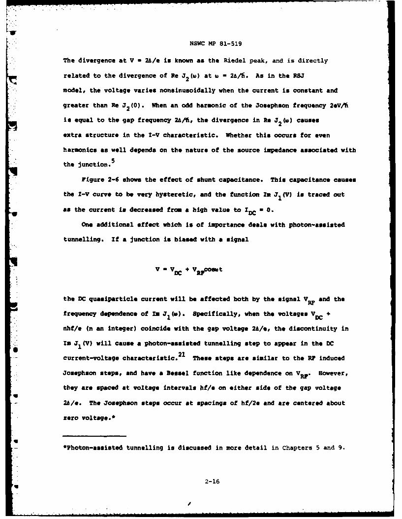
The divergence at V - 2A/e is known as the Riedel peak, and is directly
related to the divergence of Re J2 (w) at w - 2A/li. As in the RSJ
model, the voltage varies nonsinusoidally when the current is constant and
greater than Re J2 (0). When an odd harmonic of the Josephson frequency 2eV/i
is equal to the gap frequency 2A/h, the divergence in Re J2(w) causes
extra structure in the I-V characteristic. Whether this occurs for even
harmonics as well depends on the nature of the source impedance associated with
the junction.5
Figure 2-6 shows the effect of shunt capacitance. This capacitance causes
the I-V curve to be very hysteretic, and the function Im J (V) is traced out
as the current is decreased from a high value to IDC - 0.
One additional effect which is of Importance deals with photon-assisted
tunnelling. If a junction is biased with a signal
V -VDC + V" comot
the DC quasiparticle current will be affected both by the signal VRF and the
frequency dependence of Im J (a). Specifically, when the voltages VDC +
nhf/e (n an integer) coincide with the gap voltage 2A/e, the discontinuity in
I J M will cause a photon-assisted tunnelling step to appear in the DC
current-voltage characteristic.21 These steps are similar to the RF induced
Josephson steps, and have a Bessel function like dependence on VRI. However,
they are spaced at voltage intervals hf/e on either side of the gap voltage
2A/e. The Josephson steps occur at spacings of hf/2e and are centered about
zero voltage.*
*Photon-assisted tunnelling is discussed in more detail in Chapters 5 and 9.
2-16U

,-'
NSWC MP 81-519
IJv
uv- 2A/sV
FIGURE 2-5. I-V CHARACTERISTIC OF A CURRENT BIASED JUNCTION CALCULATED FROM THEWERTHAMER THEORY (AFTER MC DONALD, ET AL - REF 2)
'*..q I. 1 (1 X-4RC/2A
FIGURE 2-. EFFECT OF SHUNT CAPACITANCE ON THE CURRENT BIASED JUNCTION (AFTERIMC DONALD, ETAL - RIF2)
217
-- - -,'- ,,,,,, a~nt''
m ' -
N imi N il Iml Hidu liilimi I ii I - -I " II

NSWC MP 81-519
2.6 Calculation of the AC Impedance of a Tunnel Junction
At this stage, it may be helpful to illustrate how one can perform simple
calculations using Werthamer's equation. One calculation, which is of
considerable interest in connection with high frequency applications, is the
derivation of the small signal AC impedance of a tunnel junction. Consider tte
case where the Junction is DC current biased within the zeroth order step, and
voltage biased with a small RI signal. We have
I I DC + I cos (W t + 6) (2-18)
V - A coo Ot
Using .O - 2eV/h, the phase is 0 4o + eA sinint (2-19)
dt tio
For the moment, it Is convenient to rewr ite equation 2-1 in noncomplex
notation. Since Jl(t) and J2 (t) can be considered to be real and
causal,5 '8 the integrals in equation 2-1 can be treated as simple convolution
integrals. That is
t.t 4tt' (t' 4W 4(t) * (t) (2-20)e2 j~tt)d' e2j(t-t') dt' e 2
Equation 2-1 can be rewritten
I t)-Cosn (sin L. * J' -sin (on !L *2B c 2 1(2-21)
Using equation 2-19, we have
sin 1 : sin .O coo A sin w + coo LO sin _ sin ) (2-22a)22 (A t)2 11 (2-2a
2-18
/
NSWC MP 81-519
Cos Cos !0 co si t i _O s in sin (2-22b)
IT 2 2_o 2 iA t)
Rather than struggle with Bessel functions, it is best to limit the
calculation to the case where
eA << 1
Thus
.ini M sin 2+ Cos eA sinu (2-22c)2 2 2/
Cos lowCos !..2 - sin - =sn (2-22d)
2 2 2,'fw t
We can now compute the convolution integral.. The sign conventions used
in this thesi's are consistent with the definitions
-simt *J(t) - snwt Re J(w) + cot Im J(W) (2-23a)
cowat *J(t) - cosut Re J(W) - sinut Im J(W) (2-23b)
r Considering only the terms related to the quasiparticle current in
*equation 2-21,
. cos. (sin t. *i) -sin . (con. * .i)
[oo o - sin !o . , inwt
L 2 2 1 (2-24)
sin !...Re J.... + cos ! - i Re I I
x
'I .. + coon -$ coewt In J1 (W)J
[22-19

NSWC MP 81-519
si 2- + Cos $0 in
cos _ Re J. (o) - sin !2(sin R) J (w)]
! xsn- 0 iCOw Im Jl(w)
These expressions are apt to put many people off using the Werthamertheory. But if higher order terms (i.e., anything not at DC or w) areneglected, the expressions simplify considerably. The quasiparticle currentbecomes
IQP - eA sint ReJl(w) - Re J1(O (2-25)
+ eA coswt Im jllw)
In a similar manner, the supercurrent terms in J2(t) yield
Isc - Re J2 (0) 8ino° (2-26)
+ SA Cos ,o[Re J2 (w) + Re J2(0)] sinwt
+ Cos so J2(W] cos O
At this point, it is convenient to return to complex notation. Let
I = Re{Ippr eimt eiO + IDC
V w Re{eiwt
costt - Re •i~ t
sinwt - Re {-ieit}
The DC current is
q IDC - J J2(0) sin~o (2-27)
and the small signal AC admittance is
2-20

NSWC MP 81-519
y Re ei t (2-28)
----e O " [Re J,,' ) + Re J2 (O }
+ 1I • Re J -(w)_ ReJl(O)]
+ ImJ2w)- Cos 4o
+ I
In the RSJ limit,
Re J2(W) - ReJ2 (0 ) - Ij (2-29)
Re Jl(w) - ReJ 1 (O) = 0
ImJ (w)
7 Thus the DC current is Just
IDC= Ij sin*o (2-30a)
The AC admittance reduces to
-1 =L..+ 1 (2-30b)Rj RN imLj
where Lj A2eljcos*o
To include the effect of the Im J2(u] term (i.e., the cos s term),let
0 W
2-21

NSWC MP 81-519
y - a cos + 2eIj °s.° (2-31)0 1 0 tAt
If the junction has a shunt capacitance C, the admittance is
2el cos#y - iWC + 0 o + 00 + alcos*o (2-32)
iw
This is the admittance of a parallel RCL circuit with resonant frequency
- 2e i 0 (the plasma frequency) (2-33a)p icC
M C
and Q - (2-33b)
Returning to the high frequency limit given by equation 2-28, several
points should be noted:
1. Ii As replaced by the average of Re J2 (O) and Re 12(0)
2. At the gap frequency, Re J2 (w) diverges and the Josephson
inductance goes to zero.
3. As in the DC case, a constant in Re J1( ) is of no consequence.
4. The term e Im 3 1(w)/iw is the quasiparticle conductance. At
frequencies greater than 2A/ft (corresponding to voltages greater than 2A/e),
this quantity approaches the constant 1/%. In J (W) is presented for a
1
variety of temperatures in Figure 2-7.52 At finite temperatures and for
frequencies less than 2A, Im 1in ) can be regarded as being constant.
Thus, over a wide range of frequency, the AC resistance of the junction is
proportional to w. At finite temperatures and extremely low frequencies,
V EeImJ 1 (M1)/ again approaches 1/%. This contradicts calculations
reported in the early literature that suggest that the quasiparticle conductance
diverges at V .9
2-22
U' ' ,' . ;.'. m Q am mm mn mm E EI~ m

NSWC MP814519
5-44 TUNNELING
4
>0.
01.02.
FIGURE 27. Im J1 (t AS A FUNCTION OF TEWERATURE (AFTER YOUNG52)
NOTE: Im J (60J)uImJ (.t!.) IN THE VOLTAGE BIASED LIMIT
2-23

NSWC MP 81-519
5. In the literature, it is often assumed that1 - 2eV, and Jl and
J2 are written as functions of voltage, not frequency. If the junction
voltage is Acos, 0 t, this assumption can lead to one's using J1 (A) and
J2 (A) in calculations, when J1(w) and J2( ) are the relevant quantities.
In the small signal limit, all calculations should be independent
of A.
6. At frequencies greater than the gap frequency, Im J2 (w) is
negative. The term [e x Im J2 (w)cosw/Ti will decrease the total AC
conductance of the junction. The junction AC resistance, and consequentially
the Q of the plasma resonance, will be increased. At frequencies less than
26/A, the theory predicts that Im J ()/Im J1(w) is a positive,
temperature dependent constant that approaches +1 at T - 0.7,8
Whether this is the case in a real junction is a matter of dispute.
Lanqenberg, Pedersen, and Finnegan suggest that for a lead tunnel junction at
4.2K, Im J2 (w)/Im J1 (w) is approximately -.7 at 10 GEz.9 The above
theory suggests that this ratio should be +1 under these conditions.8
Langenberg, et al. base their conclusion on measurements of the Q of the plasma
resonance. Equation 2-33b says that if Im J2 (w)/Im J (w )
a1/ao is negative, then a plot of f /Q versus co o0 , where fp is
the plasma frequency, will have negative slope. This is what was observed in
the experiment. On the other hand, if the experiment is done at frequencies
where Im Jl(W)/w~l/w, then f Q versus Cos#o can have a negative
- slope independent of the sign of Im J2(cw)/Im Jl(w). This effect is not
sufficient to reconcile the results of the Langenberg experiment with the
theory. But it suggests that the experimental results are not conclusive. This
is discussed further in Chapter 6.
2-24

NSWC MP 81-519
7. The nonlinear quasiparticle resistance can be used for high frequency
mixing applications. Because of the reactance associated with Re J (W},
such a mixer can theoretically show conversion gain. 20 If a tunnel junction
is connected to a transmission line, the impedance of the transmission line will
Sr appear as an additional conductance in equations 2-28 and 2-31. For many
applications, it is assumed that one wants to match the transmission line
impedance to the normal-state resistance of the junction. In terms of the
conductance of equation 2-28, this matching condition will hide the .esired
nonlinear effect of Im J (w). To operate a tunnel junction quasiparticle
mixer with gain requires that there be a mismatch between the junction and its
microwave surroundings.
2-25/2-26
NSWC MP 81-519
CHAPTER 3
ELECTRONIC SIMULATION OF THE RSJ MODEL
3.1 Introduction
r Calculations based on either the Werthamer or RSJ models are usually quite
intimidating. There are few analytic solutions, and perturbation theories are
complicated and tend to diverge. 22 Digital calculations are difficult, use
much computer time, and occasionally give misleading results. To include the
effects of capacitance, source impedance, and time dependent sources in a
calculation only makes the problem worse. 2
The motivation for using an electronic analogue stems from the extremely
close similarity between the RSJ model of a Josephson junction and a
phase-locked loop. The correspondence between the two is quite direct in that
phase, voltage, and current in one are equivalent to phase, voltage, and current
in the other. Mathematically, the only difference between the two is in the
sizes of IJ, RN, and 2./h. However, this allows one to make an extremely
Lwide variety of measurements on an analogue that would be difficult to make
using a real junction. In terms of speed, simplicity, ease of changing
parameters, and ease of interpreting results, an analogue compares favorably
with digital methods. The accuracy of measurements obtained using an analogue
is often quite good, and there are certain cases where an analogue neatly avoids
pitfalls that beset even the most carefully performed digital computations
(i.e., calculation of subharmonic step heights).
3
'- 3-1
U-.
NSWC MP 81-519
3.2 Existing Analogues
The original phase-locked loop analogue of the Josephson effects was
reported by Bak and Pedersen in 1973.4 There have been various other
analogues reported in the literature, most of which are also phase-locked loop
designs. Before discussing the design and use of a Bak type analogue in detail,
we sumarize the principles of several analogues.
The Mak and Pedersen Analogue 4
This is basically a phase-locked loop containing a voltage to current
converter. With reference to Figure 3-1, there are five distinct building
blocks in the circuit. They ares
VCO Voltage Controlled Oscillator
LO local Oscillator
Jx Multiplier
LPF Low Pass Filter
VCCS Voltage Controlled Current Source
The VCD generates a signal
VVCO Alsin(mt + IVindt) (3-1)
where Vin is the voltage at the input to the device. The quantity K is known
at the VCO gain constant, and is the analogue of 2./h in a real junction.
The local oscillator produces a signal
cVLo - a2osmot (3-2)
Note that Al' A2 , and K are independent of Vin. The outputs of the VCO
and LO are multiplied to produce a signal
3-2

NSWC MP 81 -519
FL
FIGURE 3-1. THE BAK AND PEDERSEN ANALOGUE
3.3
NSWC MP 81-519
V14UTJ JJ, el in nd + sin jiiait + a'v'acl (3-.3)2 [itA3 JinO Jfl
where A3 is the conversion gain of the multiplier.
The LPF serves to remove the signal at 2w from the output of the
multiplier before the signal reaches the VCCS. We have
VLPP 1 AiA2A3A4 8in (3-4)2
where A4 is the low frequency gain of the filter, and d#/dt - n.in
The VCCS generates a current
I U- IlA 2A3A4sin (3-5)2
where G is the transconductance of the current source. If we define
j lrGA 1AjA 2A3A4
we have for the current Il in Figure 3-1,
I, - Ijsins (3-6)
At this point, it is stressed that the VCCS can act as both a source and
sink of current, and that essentially no current flows into the VCO, it being a
high input impedance device.
The output of the VCCS is connected to the input of the VCO. With the
addition of a resistor in parallel with the input, the current-voltage
relationship of the overall circuit is
-I sin# + Vin where " KV (3-7)R dt in
23,24Analogues of this form have been widely used. The main advantages
Iof this scheme are its simplicity and the dimensional correspondence between
parameters in the analogue and those in a real junction. This makes it easy to
3-4
'I

NSWC MP 81-519
model the effects of shunt capacitance, finite source impedance, etc. An
additional advantage is that the sin kfVindt dependence of the analogue isiIn
implicit in the operation of the VCO.
There are two major disadvantages to the Bak scheme. First, the LPF
p introduces a frequency dependent phase shift to the sin# signal. This results
in the addition of a voltage dependent cos term to the overall
current-voltage relationship of the device. The amplitude of this term is
always negative with respect to the sign of IJ. This amplitude can be made
quite small, but not always as small as one might like. The other disadvantage
is that the phase of the supercurrent is not directly accessible-that is, there
is no signal proportional to #. This prevents the analogue from being used to
model double Junction SQUIDs or other devices where both * and sin# are of
25interest.
The Gallop Analogue*
An analogue based on the Bak principle, but having a nonsinusoidal
* current-phase relation, was built by Gallop. The device is extremely simple, as
the VCO, LO, multiplier, and LPF are incorporated into one phase-locked loop
chip. This chip operates in a digital switching mode. That is, it operates
using square waves, as opposed to sine waves. This precludes its use for
quantitative measurements, but the device will qualitatively model the Josephson
effects.
The Taunton and Halse AnaloguS 26
- This is basically a quadrature version of the Bak analogue. In addition to
the sin# term, there is a second feedback loop that models a cos term.
*J. Gallop, private cownunicatLon.
3-5
4i NSWC MP 81-519
This term is made voltage dependent by the inclusion of a field effect
transistor in the cosine loop. This FET gate is connected in such a fashion
that it models both the a Vcos term and the a V term in equation1 0
*2-5. Since the sin# and cos# terms are independent, and not related via the
lramers-Ironig relations, the amplitude and sign of a1 with respect to IJ
and a o is arbitrary.
The circuit has been used to investigate the effects of thermal noise and
the influence of the cos term. Good agreement with theory is reported,
although the effect of the cos# term is undramatic. The circuit is much more
complex than the Bak analogue, and suffers from stability problems.* In
addition, the problem of an unwanted phase shift associated with filtering the
outputs of the multipliers may result in the introduction of a coso term in
the sine loop, and a sin$ term in the cosine loop. However, the circuit seems
to have produced useful results.
27
The Hamilton Analogue
This is based on a more traditional style of analogue computation than the
Bak analogue is. The equations
dax (kV )y _d - (-kV )x (3-8)dt in dt in
2 2are solved subject to the constraint x + y =
1 2J. This results in the signal y having the form
y = I sir*, where At. - kV (3-9)J dt in
*M. R. Halse, private communication.
3-6wu

NSWC MP 81-519
The circuit in built using integrated circuit multipliers, integrators,
inverters, and summers. Unlike the Bak analogue, there is no distinct VCO, LO,
or LPF. Although the circuit seems reasonable and is relatively simple, it has
not been widely used. It may offer advantages over the Bak circuit, as unwanted
P high frequencies (i.e., 2"o in equation 3-3) are not generated. On the
other hand, the integrators probably introduce a cosa term similar to that
caused by the low pass filter in the Bak analogue. And the use of five
multipliers, as opposed to one in the Bak analogue, will increase the noise,
harmonic distortion, DC offset error, and cost.
The Magerlein Analogue28
In this analogue, there is no VCO or LPJ. Instead, the input voltage to
the analogue is integrated explicitly, and the resulting voltage passed through
a sine conversion circuit. That is an integrator converts d/dt into #, an
another circuit takes the sine. The sin4 signal is then passed through a
voltage to current converter, and fed back to the input. The advantage of this
Le arrangement is that a signal proportional to # is directly available. The
disadvantages are that the integrator must be reset whenever t reaches the
voltage corresponding to w/2 (or the device will saturate), and the sine
conversion circuit is not necessarily very accurate. The integrator is reset
using a flip-flop to drive an electronic switch. This has the unfortunate
result of putting a glitch in the Josephson oscillations every time the
integrator resets. A copy of the Magerlein circuit has been built and tested by
Brady.*
*R. Brady, private communication.
3-7
.... . ------ - - - -- .mm m datm*- a a i ~ lln m I °

NSWC MP 81-519
The Tuckerman Analoque25
This is an analogue of a complete DC SQUID. It is essentially two
Magerlein analogues connected to form a *superconductingn loop. Gyrator
circuits are used to model the inductance of the loop. (A gryator is a
nonreciprocal amplifier circuit that can be used to make a capacitor look like
an inductor.) The analogue suffers from the problems described for the
Magerlein analogue. However, as the phase is required explicitly, one could not
use a Bak type circuit instead.
The Yagi and lurosava Analoque 29
This is a precision version of the Magerlein analogue. The major differenceV
between the two is the manner in which the sine conversion circuit operates.
The Nagerlein analogue uses a simple circuit based on the nonlinear behavior of
a bipolar transistor. The Yagi simulator uses a series of transistor switches
to create a five segment piecewlse-linear approximation to a sine wave. The
Yagi analogue also incorporates a network for modelling the nonlinear resistance
associated with a tunnel junction. This consists of a two step piecewise-linear
resistance circuit. There is no reactance associated with this, so it is not a
true model of the nonlinear resistance described by the Werthamer theory.
The Prober Analoaue
Prober, et al. have developed an analogue of the RSJ model in which the VO
generates short pulses rather than the usual sine or square wave. The
pulses drive a sample and hold circuit which cleverly fashions a stair step
approximation to sin# without the need for a low pass filter. The circuit,
which also incorporates a voltage dependent conductance for modelling the
nonlinear quasiparticle characteristic, Is simple and works well. However,
3-8
IMP

NSWC MP 81-519
there is a phase shift associated with the sample and hold technique which
introduces a negative coso amplitude similar to that expected for a low pass
filter.
3.3 Design of an RSJ Analogue
In retrospect, the design of an analogue based on the Bak scheme is not
very difficult. Of the five components, the VCO, LO, and multiplier require no
special design considerations. The VCCS and low pass filter use standard
circuit topologies, and computation of component values is not difficult.
The operating parameters of the device were chosen such that simple circuit
techniques could be used, and so that the effects of circuit noise and parasitic
capacitance are negligible. For the preliminary design:
Ij -lmA
%N 1 W
2e/h - 1000 hz/volt
f 1 o fvco - 1S kHz
The half power frequency of the low pass filter is 5 kHz.
The first three parameters are variable. The VCO center frequency can be
fine tuned to equal that of the LO. This is to make the DC supercurrent occur
at zero DC voltage. If f10 * f vco this *zeroth order step" will occur at
finite voltage, and the entire I-V characteristic of the device will be shifted
along a load line determined by RN. This does not affect the shape of the
characteristic, or the junction dynamics.
The VCO and LO are built using Intersil 8038 function generator chips.
Their frequency of operation is determined by the appropriate choice of a timing
3-9

NSWC MP 81-519
capacitor. The value of 2e/h for the VCO is determined by an external
amplifier. The harmonic distortion of the 8038 is less than 1 percent at
15 kHz, but there is noticeable drift in the operating frequency due to thermal
effects. Fortunately, this has minimal effect on the use of the analogue. The
complete design details for the 8038 are described in a manufacturer's
applications note.
The mat tiplier is an Analogue Devices ADS30KH. Over its range of
operation, its accuracy is quoted as 1 percent. The main disadvantage of the
chip is that it requires three external presets.
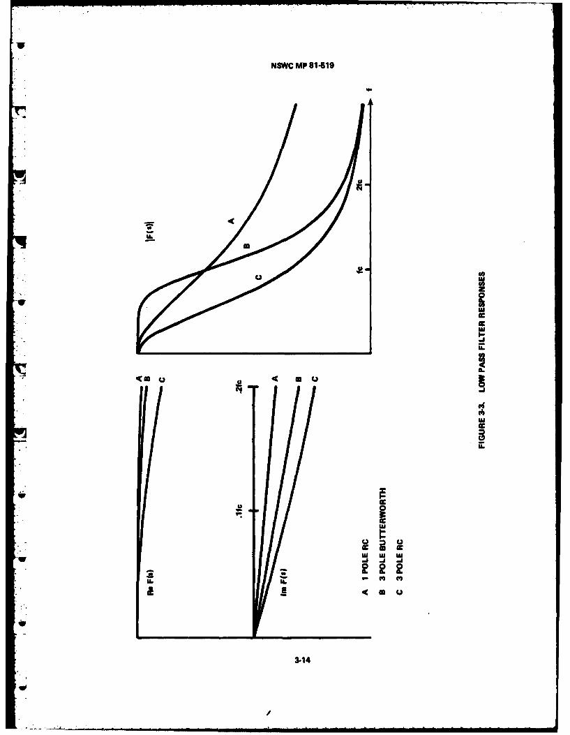
The VCCS is a stardard des1,,n, fully described in Motorola Applications
Note AN-587. It can act both as a current source and a current sink, and the
output impedance is easily mad* greater than 300 kQ. With reference to Figure
3-2, we have
I -Vin (3-10)out R
R + RT( R3 _ 2)a3 LR 4 R1/
Z [R3 (3-11)out [iR _ R ]
4 The device is very linear, and can provide several milliamps. However, the
circuit will clip if the voltage at the output of the op amp approaches the
supply voltage. This, rather than the power rating of the amplifier, is usually
the limiting factor in how much current can be provided.
Although the design of the low pass filter is not complicated, its effect
on the behavior of the analogue is slightly subtle. The phase shift of the
3-10
/

r NSWC MP 81-19
R2
VIN
FIGURE 3-2. A VOLTAGE CONTROLLED CURRENT SOURCE
3-11

wI
NSWC MP 81-519
filter introduces a negative cos* term into the analogue. To see this,
consider the single pole filter response given by
1 - j w/nF(Jw) - C (3-12)
1 + c~~
where wc is the half-power frequency.
This response can be realIzed using a resistor and a capacitor; the
resulting filter is referred to simply as an PC filter. When the analogue is
biased with a constant voltage, the output of the multiplier will be of the form
V - sinwt + sin (2w t + Wt)0
The filter will eliminate the high frequency component, leaving a voltage
VLpF - sinwt Re P(jw) + cos wt Im P (jw)
If w < w
Re F(jw) =1 (3-13)
Im F(jW) -W/Wc
and
V r l. - w/wcoswt
VP = sinwt-wncot
This changes the equation for the loop to
I -lj sin* -_!J+cos* + - N (3-14)
R wc RN
awhere Wj m 2e R/16, .. - -__ (cf. (Eq. 2-31)
C o wc
3-12
'w

NSWC MP 81-519
The voltage dependent cos term has the same form as the
r quasiparticle-pair interference term in equation 2-5. Bak and Pedersen have
utilized this similarity to investigate the effect of a negative cos# term on
the dynamics of a Josephson junction.4 '31 For most applications, this term is
unimportant. 8 However, it does affect the high frequency impedance of the
device slightly, and can have a noticeable influence on the Q of the plasma
resonance.
It was found that the single pole RC filter was not entirely effective in
reducing the signal at frequency 2w 0 + w. Rather than increase theo
frequency of the local oscillator, a more sophisticated filter was used. The
* filter, a three pole Butterworth, has the same half power frequency as the RC
filter, but its response falls faster at high frequencies. This is evident in
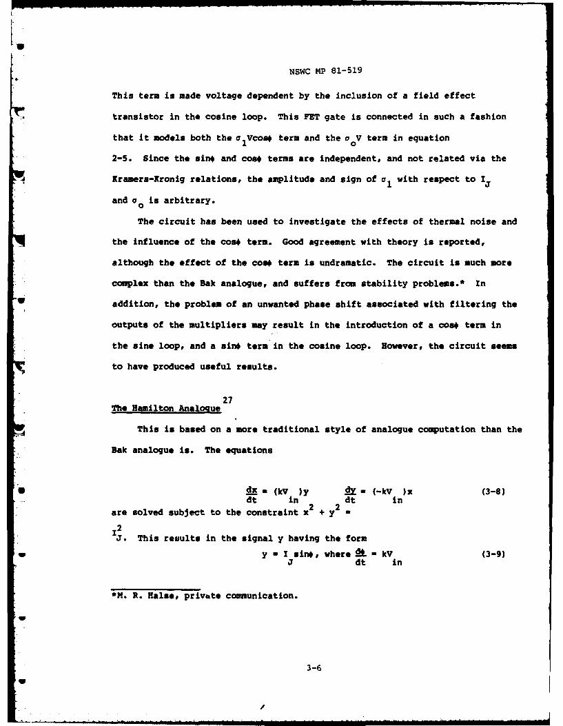
Figure 3-3, which shows the response curves for a one pole RC, three pole RC,
and a three pole Butterworth filter. The respective response functions are:
F.s' " F a) = 1 one pole RC (3-15)1+3
1F(s) 1 three pole RC(1 + )3
F (S) = 1 three pole Butterworth83 + 2s 2 + 2s + 1
where s Jo/oc -
All three filters in the figure have the same value of w . Note thatc
the tradeoff for reduction of high frequency feedthrough is an increase in the
amplitude of Im F(s), and consequently an increase in the coas amplitude.
For typical parameters of Ij = 1 mA, RN - 500 ohm, and 2e/h - 500
Hz/volt, we have waj/wc = .05. Multiplying by 2 (since the Butterworth
filter increases the cos# term by about that much), we have a1/00 = -0.1.
3-13
NSWC MP 81-519
I,
co U =
InA
A16 IL4c co Q
3-14

NSWC MP 81-519
For most applications of the RSJ analogue, a cos* term of this magnitude will
U be unimportant. Provided that one is aware of it, it does not limit the
usefulness of the analogue. From a design point of view, the three pole
Butterworth is only slightly more complicated than the one pole RC filter.
p Using the building block6 described above, the final design of the analogue
in straightforward. However, before describing the use of the analogue, there
are two more circuits that should be mentioned. The first of these is a
multiple input current source for use in driving the analogue. It is similar to
the VCCS in Figure 3-2, but allows for mixing of several different input
signals. The second circuit, suggested by N. Dett of the Cavendish electronics
section, is used to voltge bias the analogue. With reference to Figure 3-4,
the voltage V is equal to Vn, and the signal V provides a referencea ion
voltage which is proportional to the current through the analogue. The voltage
V is provided by the multiple input current source described above, Ra is
a variable source resistance. The voltage and current sources are connected
with switches so that the analogue can be changed from voltage to current bias
at a moment's notice. By raising R to a large value, the voltage source
looks like a reasonable current source, but its dynamic range under these
conditions is limited.
If proper attention has been given to the selection of part values,
operation of the analogue is not complicated. When all of the building blocks
are connected, it is necessary to adjust IT, k, and R to suitable values.
This usually means keeping kIjR/uc << 1, so that the LPF does not
attenuate higher harmonics of the Josephson oscillations. If one wishes to
3-15
I

NSWC MP 81-519
TO ANALOG v
L + V~men CL
FIGURE 3-4. A VOLTAGE SOURCE
3-16

NSWC MP 81-519
investigate the condition a -1 , which requires that k1jR/wC
*1, the analogue must be operated at frequencies much less than wi or the
*results will be inaccurate.
• 3.4 Results Obtained with the RSJ Analogue
As the Bak analogue has been widely investigated by others, this section is
relatively brief. Figure 3-5a shows the time averaged current-voltage
characteristics for the analogue under current bias, voltage bias, and finite
source impedance conditions. Figure 3-5b shows the effect of microwaves" on
- the I-V characteristics. Figure 3-6 shows the voltage as a function of time for
r three values of IDc for the current biased case, without microwaves. Figures
3-7 and 3-8 show the effects of varying the frequency and amplitude of the
applied RF signal under current bias conditions.
Within a current step, the fundamental frequency of the internal
oscillations of the analogue is an exact harmonic of the frequency of the
applied R current. Figure 3-9 shows the voltage as a function of time for the
analogue when current biased within each of the first several steps in the I-V
characteristic. Note that the signal is periodic, and that the number of pulses
per cycle is equal to the =order= of the step. That is, the nth step, which
occurs at a DC voltage equal to V - n16 /2e, has n pulses per cycle. McDonald
has suggested the use of this phenomenon for pulse generator applications.3 5
Figure 3-10 compares a result obtained with the analogue with a computer
calculation by Waldram, et al. 33 The parameters of the calculation and
analogue measurement are similar, but there are no subharmonic steps in the
analogue result. The 383 model predicts that outside of a step, the voltage
will be an almost-periodic function of time. It is the author's hypothesis that
3-17
.. , ,.. ,_. ,.. .,=,i. t . .,r~lir i i i i i= i i I i i i| i . .
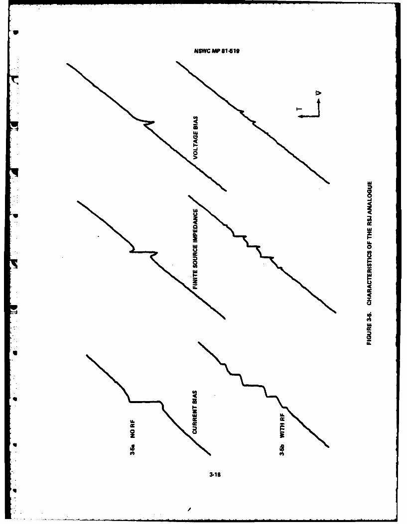
NSWC MPB81419
uI>
0
I.-L
0
414
w
3-1-

NSWC MP 81419
p
A46V INCREASING
IA A A boc
In I SINO+ V
Vft) -V11+2 ~i:!)Cos nwot]
FIGURE 3-&. Vf1 I FOR THREE VALUES OF lDC
3-19

NSWC MPS161
* 0
U U
4..
3-20

N8WC MP 81-519
'0-0
+, 8
U0
3-21.
NSWC MP 81 -519
40ju
0TH STEP
IZ 3RD STEP
4TH STEP
5TH STEPAt TH STEP
FIGURE 3-9. V(0) WITHIN A CURRENT STEP
3-22

NSWC MP 81-519
z7 0
z
U
70 15 .zc
cc I-
C-44
-C44
4L
3-2

INSWC UP 81-519
the computer calculation was not accurate enough to distinguish between periodic
and almost periodic behavior in certain regions, and that subharmonic steps
appeared as a result. This is an example of a calculation where the analogue
avoids pitfalls that can be quite difficult to prevent in a computer calculation.
Figures 3-11 and 3-12 show the AC impedance of the device under conditions
where the analogue is current biased by a signal I - I DC IRcoswt. The
impedance is measured by multiplying the voltage across the analogue by a
reference signal that is either in phase or 90 degrees out of phase with the
applied RP current. The time averaged output of the multiplier is proportional
to either the real or imaginary part of the impedance at frequency wi. The
V results obtained using the analogue are compared with the computer calculations
of Auracher and Van Duzer, which are shown as insets in the figures.34 The DC
I-V characteristics are plotted to show the relation between the junction
impedance and the location of current steps in the characteristic. Note that
the reactance beteen steps is zero. This results from the almost periodic
nature of the AC voltage across the junction when it is biased between steps.
The instantaneous reactance may be finite, but the time averaged reactance is
zero. Within a step, the RSJ analogue works very well, but there is spurious
interference between steps. This measurement is a good qualitative indication
of the accuracy that one can expect from a simple analogue.
If there in a capacitance in parallel with the analogue, it will add a
negative term to the total junction reactance. Within the zeroth order step,
this will cause the total reactance to cross through zero at a particular value
of DC current. This corresponds to the DC current for which the applied
frequency is equal to the plasm frequency.
3-24
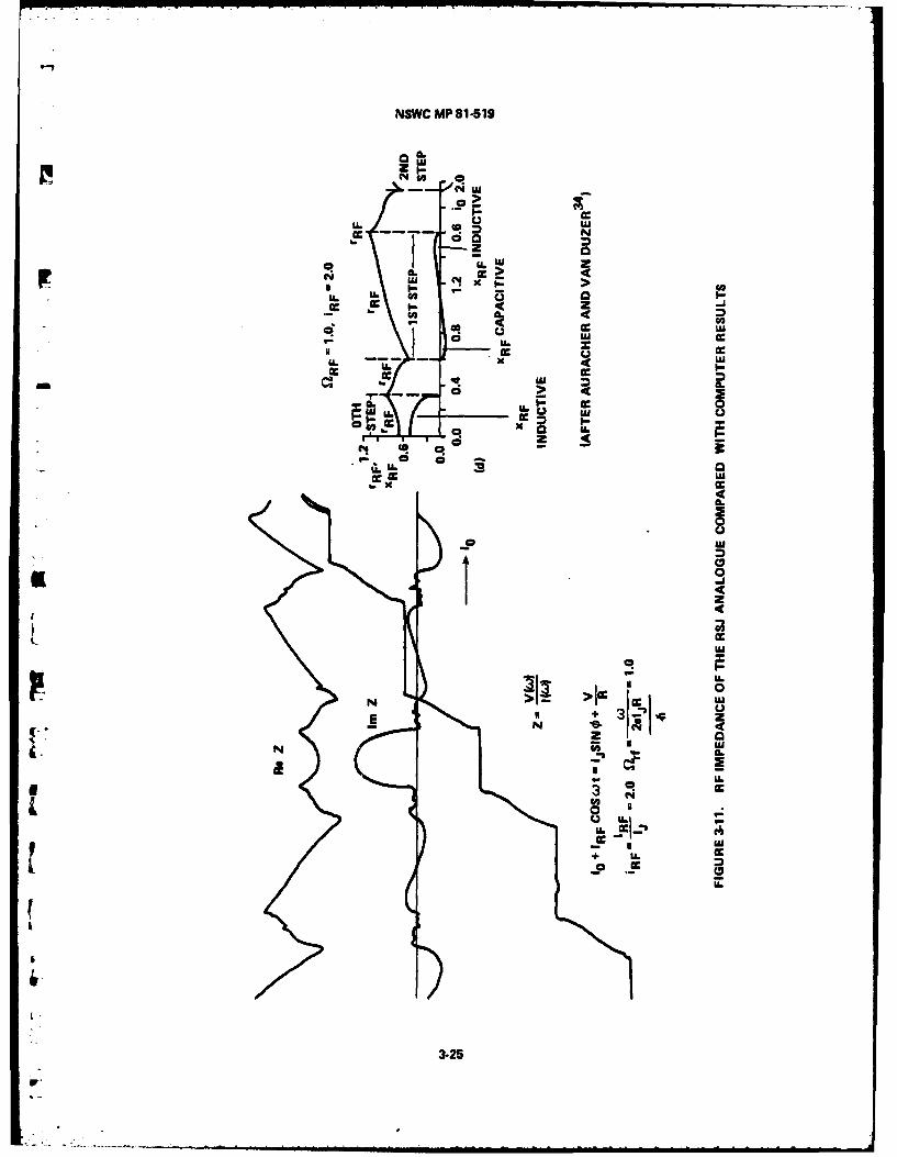
NSWC MP 81-519
m:I
a . I-
W6 C
U. U
*Ui
404LL W6 Gcc 0
I zU
0* I-.U~cc
b* 0N ~~> j W
U.U
* IL
3.25
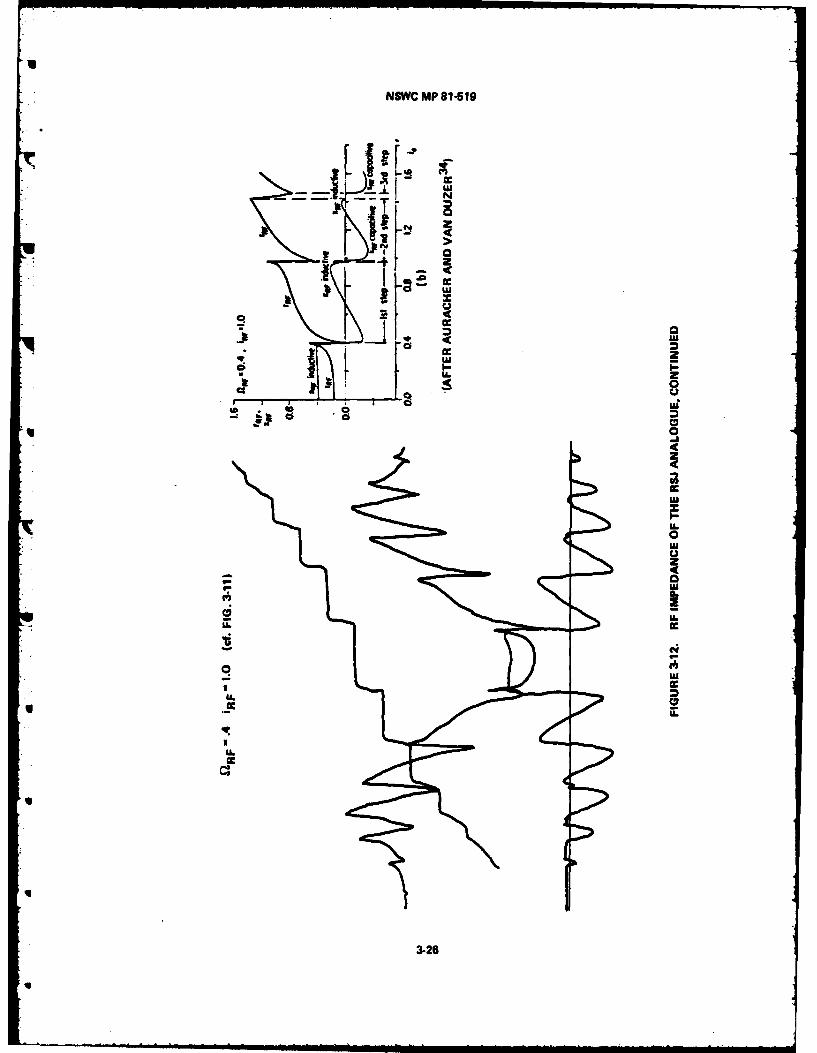
NSWC MP 81-519
UL
z-Cc -
0
LU
U.ccIl
W6
c:t
q3-26

W
NSWC MP 81-519
CHAPTER 4
ELECTRONIC SIMULATION OF THE HIGH FREQUENCY THEORY
4.1 Introduction
rThe high frequency analogue is based on an idea by Waldram, who suggestedthat the Werthamer theory could be modelled electronically using a quadrature
phase-locked loop and some sophisticated filters.6 As shown in section 2.6,
equation 2-1 can be written
I (t) - cos 2. (sin 2 * i ) - sin 2 8 cost2 * (4-1)(a 2 ) 2 c+ sin 8!. L ) + cos in * jr-2 222
where the terms in brackets represent convolution integrals of the form
[ in * Ji " sin 4W) j (t-t-) dt' (4-2)\s 2 1 /f 2 1
Electronically, this integral is the equivalent of running a signal sin
*/2 through a filter with impulse response j1 (t). As jI(t) and j2 (t)
can be regarded as being real and causal, filters with suitable pulse responses
can, in principle, be constructed.
The complete simulation of equation 4-1, including the generation of the
sin */2 and cos#/2 signals, is done using an elaboration of the Bak scheme
described in the previous chapter. The essential differences are the inclusion
of the filters and the use of two local oscillator signals instead of one. The
scheme used is shown in Figure 4-1.
L
4 4-1
.... -. ,.,..,,.,+l..t.. - - b i Im l l=,'i ll l I N

NSWC MP 81-519
SIN TX
'. "VCO VOLTAGE CONTROLLED OSCILLATORLO LOCAL OSCILLATOR
S PHASE SHIFTER
VCCS VOLTAGE CONTROLLED CURRENT SOURCELPF LOW PASS FILTERI INVERTER
3 + ADDER
FIGURE 4-1. BLOCK DIAGRAM OF THE HIGH FREQUENCY ANALOGUE
4-2
4q
NSWC MP 81-519
The operation of the building blocks is identical to that in the Bak
analogue. The only new component, apart from the filters, is the 90 degree,
- unity-gain phase shifter. This provides a quadrature reference to the local
oscillator, which in turn allows the generation of both sin #/2 and cos#/2
signals. The VCO gain constant k now represents c/h instead of 2e/h. If the
J1 filters are omitted, and the J2 filters bypassed (i.e., - J2( ) - 3),
the circuit in Figure 4-1 reduces to a complicated version of the Bak analogue.
The prototype of the high frequency analogue is reported in a paper by
Jablonski and Waldraa, 35 a copy of which is attached as Appendix A. The paper
.1 is a self-contained description of how simple filters were used to model j1 (t)
q - and J2 (t), and what results were obtained when these filters were incorporated
into a quadrature phase-locked loop. The loop was built using the circuits
described in Chapter 3, with additional filters based on calculations by
Le Waldram, who matched the response curves of simple three and four pole RLC
networks to sketches of Werthamer's expressions for J() and J2 (W) at
T - 0. Although the prototype demonstrated the feasibility of the high
* frequency analogue, the filters were not accurate enough for the analogue to be
very useful.
Attempts at improving the filters were made by P. Sinclair as part of a
final year undergraduate physics project.* This effort was based on
L constructing several sets of electronic filters having adjustable parameters.
Using what were essentially trial and error techniques, the parameters were
L varied to model J1 (I) and J2 (w) at a variety of temperatures.
Unfortunately, this was not very successful.
*P. L. Sinclair, private communication
4-3
NSWC MP 81-519
Simple numerical methods used by the author, however, proved quite
successful for modelling J l (w) and J2 (w) at T - 0. The increased
accuracy of the resulting filters made it necessary to improve the performance
of the quadrature phase-locked loop circuit. This chapter describes the design
of the loop, the design and construction of the improved filters, and the
results obtained with this second version of the high frequency analogue.
4.2 Design of the Loop
The prototype analogue had problems with harmonic distortion and
temperature drift in the LO and VCO circuits. To cure this, these circuits were
replaced by two commercial signal generators. One, with quadrature outputs, was
used in place of the LO and phase shifter. The other was used as a VCO. The LO
*frequency of the analogue was set to 60 kHz, the maximum frequency of the
quadrature generator.* The previous problems of harmonic distortion and drift
essentially disappeared.
The six multipliers and the VCCS are the same circuits used in the Bak
analogue. The low pass filters are four pole Butterworth's with a half power
frequency of 50 kHz. The equivalent cos# amplitude (cf. Eq. 3-14) is -.04.
The effect of this term on the current-voltage relationship of the analogue is
not as simple as before, as the unwanted phase shift of the low pass filters
- affects both the sire/2 and cos#/2 signals. However, provided that this
phase shift is small, it can usually be neglected. The only measurement where
this proved to be important was the investigation of the Q of the plasmaV
resonance.
*In later versions of the analogue, the LO frequency was increased to 100 kHz,V
then subsequently reduced to 30 kHz (cf. Chapter 8).
4-4
V

NSWC MP 81-519
Typical operating parameters of the analogue, along with the equivalent
values for a real junction, are shown in Table 4-1.
4.3 Design of the Filters
All of the information concerning temperature, high frequency effects, and
energy gap effects is contained in the expressions for jI(t) and j2(t).
Consequently, the accuracy of the analogue is largely a question of the accuracy
of the filters.
As was shown by Sinclair's work, the extension of Waldram's curve fitting
techniques to more complicated filters is not very practical. Efforts were made
by the author to match Werthamer's analytic expressions for Jl (W) and
J2 W) at T - 0 to the generalized expansion of a multipole RLC response, but
it proved impossible to systematically match the Lorentzian behavior of the RW
Unetworks to the logarithmic behavior of the Werthamer expressions.I rA numerical approach was tried next. This was based on matching the
response of a multipole RNW network to the numerical values of J1 (w) and
J2 at an arbitrary number of frequencies. This method was suprisingly
successful, and has the advantage of being useful for designing filters to model* - tunnelling at T P 0, where analytic expressions for Jl(u) and J2(a) do
4 not exist. This numerical method is described below.
The response of an RLC network can be expressed as
rF) a + a a + a s 2 + ... + a an-1- (0) 0 1 2 n-i (4-3)
1 + Ala + A2S4+... + Ansn
where s =ju
4-5

NSWC MP 81-519
Table 4-1 Typical Parameters of the AnaL- ,e Compared With Those
of a Real Superconducting TUnnel Junction
The Analogue A Tunnel Junction
.7 mA 1 mA
RN 1500 ohm 2.5 ohm
2e/h 1500 hz/volt 483 MHz/ovolt
f - 2 A/h 1000 hz 725 Gzigap
V g 2a/e 1.33 volts 3 nV. gap
4-6
V
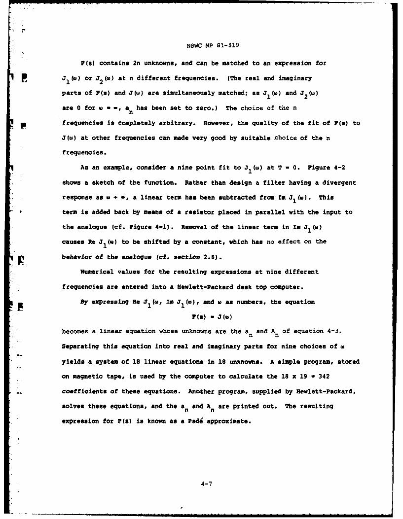
NSWC MP 81-519
F(s) contains 2n unknowns# and can be matched to an expression for
Jt W1() or J 2(W at n different frequencies. (The real and imaginary
parts of F(s) and J(w) are simultaneously matched; as J 1(w) and J 2(W
are 0 for as - -, a nhas been set to zero.) The choice of the n
frequencies is completely arbitrary. However, the quality of the fit of F(s) to
3(w) at other frequencies can made very good by suitable choice of the n
frequencies.
As an example, consider a nine point fit to J3 (ws) at T - 0. Figure 4-2
shows a sketch of the function. Rather than design a filter having a divergent
response as ws.. a linear term has been subtracted from rm 1(W). This
term is added back by means of a resistor placed in parallel with the input to
the analogue (cf. Figure 4-1). Removal of the linear term in Im 1 W)
causes Re J 1 (w) to be shifted by a constant, which has no effect on the
behavior of the analogue (cf. section 2.6).
Numerical values for the resulting expressions at nine different
* frequencies are entered into a Hewlett-Packard desk top computer.
By expressing Re J 1 (as Xm 1 (w), and ws as numbers, the equation
F (s) - J W)
becomes a linear equation whose unknowns are the a and A of equation 4-3.n n
Separating this equation into real and imaginary parts for nine choices of as
yields a system of 18 linear equations in 18 unknowns. A simple program, stored
on magnetic tape, is used by the computer to calculate the 18 x 19 - 342
- coefficients of these equations. Another program, supplied by Hewlett-Packard,
solves these equations, and the a nand A nare printed out. The resulting
expression for F(s) is known as a Pad4 approximate.
4-7

NSWC MP 81-419
r Re J1 Cd
4-2a J1 (WiJ
rIm
J, '
4.2b J1(w) WITH LINEAR TERM SUBTRACTED FROM tnt JIM,4 AND Re J1(Co) SHIFTED BY A CONSTANT
Re J2 WCI
4-2c J2fA)
FIGURE 4.2. SKETCH OF THEORETICAL J1 (CA) AND J2((A)) FOR T *0
4-8

NSWC MP 81-519
To verify that the Padf approximate can be implemented using electronic
Ufilters, it is necessary to factor the denominator and check that all of the
poles of F(s) lie in the left half of the complex frequency plane. This is
doen using a modified version of another Hewlett-Packard program. If the Pade
approximate proves to be causal, a fourth program is used to plot F(s). If the
expression for F(s) is not causal, or the plot does not look like J(W), the
whole process is started again using a new set of trial frequencies.
If F(s) is a good match to J(w), a program is used to calculate a
biquadratic partial fractions expansion of F(s). That is, F(s) is written as
F(s) - m + n n (4-4)
n-- 82 + ans + bn n
By using the ratio of two quadratics, the coefficients a, b, c, d, and m
will always be real. As will be seen, this form of F(s) is particularly
amenable to synthesis using active electronic filters.
Figure 4-3 shows a plot of the calculated nine pole Pad' approximate to
J (W) at T - 0.* The x's show the points at which the Padg approximate is
equal to the theoretical expression for J(). The overshoot at the gap
frequency is similar to the Gibbs phenomena associated with the use of Fourier
techniques to model a discontinuity. Figure 4-4 shows the individual
biquadratic components of the Pade approximate. Each curve corresponds to the
response of a one or two pole RLC network, and can be viewed as being the
combination of low pass and bandpass filter responses. Note that the parameter
m for each filter is zero (i.e., the high frequency response of each filter goes
*The linear term in Im Jl(w), which was subtracted prior to the calculation.has been added to the result plotted in Figure 4-3. The corresponding constantin Re Jl(w), however, has not.
4-9

NSWC MP 81 -519
3
C
ILI
'U.
t I I
14-1

NSWC MP 8119
UU
w H
CCI
0
- I-
,I-1-
\ -, i U.
EA
cc .
4-112

-
NSWC MP 81-519
to zero). Inspection of the individual curves suggests that trial and error
techniques to determine the filter parameters would have been very difficult.
Figure 4-5 and 4-6 show the corresponding nine point fit to J2(W),
along with its biquadratic components.
4.4 Construction of the Filters
The filters were built using an active op amp circuit known as the36
"biquad". The circuit, shown in Figure 4-7, has a transfer function
V 2
Vout . ms + cs + d (4-5)
* Vin s2 + as + bwhere s - Jw
The parameters a, b, c, d, and m are determined by appropriate choice of
component values. The relative signs of c and d are determined by whether the
point X in the circuit is connected to Y or Y'. Setting m a 0 is accomplished
by removing R7 from the circuit.
The performance of the biquad is comparable with, if not better than, its
passive REC equivalent. 37 As it contains no inductors, and has no special
interface requirements, it is actually more convenient to design and use. An
entire biquad costs about the same as the ferrite core needed for a single large
inductor.
The choice of component values is very flexible. The main limitation is
that R1C 1 should equal R3 C 2 . This ninimizes the sensitivity of the Q to
W variation in component values. For an arbitrary choice of a, b, c, and d (m is
assumed to be zero), subject to the constraint R1C1 - R3C2, five
component values must be computed. In the actual filters used in the analogue,
V
w 4-12

NSWC MP816519
0
jr LI
L-
g cc
4-13

NSWC MP 81-519
3
E
LU
I'
4,
uu
ii
U.U
w
4-14
.-. ,=.i.,--. "' 'm i lam. mlmis i i i i i i l u - L i.. ...-

NSWC MP 81-519
VIN RC 2
+ vt - V
- I +
I - I+V~ I I
FIGURE 4-7. A BIQUADRATIC FILTER
p
4-15
NSWC MP 81-519
each calculated value is implemented using two components. For example, if the
calculated value for R. was 49,260, R6 would be wired in the circuit as a
47k resistor in series with a 2.2k resistor.
To model the nine point fit to either Jl(W) or J2 (w) requires four
biquads with two poles each, and a low pass filter having one pole. The filters
are wired in parallel. That is, they all have the same input signal, and their
outputs are summed.
Figures 4-8 and 4-9 show the measured response of the filters built to
model the nine point fits to J(w) and J2 (w) at T - 0.
With reference to Figure 4-1, two J1 (w) and two J2 (w) filters are
10 used in the analogue. By using filters having response functions (J1 + J2)
and (J1 - J2), this redundancy could have been avoided. However, the use of
duplicate Jl and J2 filters permits separate control of the pair and
quasiparticle currents, which is a useful feature of the analogue. Figure 4-10
shows the response curves of the duplicate filters used in the analogue plotted
together. Note that the resonance peaks occur at slightly different
frequencies. Although undesirable, this inaccuracy does not appear to be a
major shortcuming of the analogue. This problem is discussed in greater detail
in Chapter 8.
To adjust the Otemperature" of the analogue, it is necessary to modify
JI(w) and J2 (w). Unfortunately, preliminary attempts to do this by
designing additional filters failed consistently. For the T 0 0 case, the Pade
approximate technique kept resulting in nonrealizable filter responses, where
one or more of the poles of F(s) were in the positive half of the complex
frequency plane. This problem was overcome eventually (cf. Chapter 7).
However, results presented in this chapter are limited to the case where theV
analogue models Josephson tunnelling at T - 0.
4-16
n uw- ° '-

NSWC MP 81419
____ ____ ___ ____ __ ____ _ _ ____ __ .46 kHz
p
FIGURE 4-8. MEASURED RESPONSE OF THE J, (W) FILTERS
4-17
-
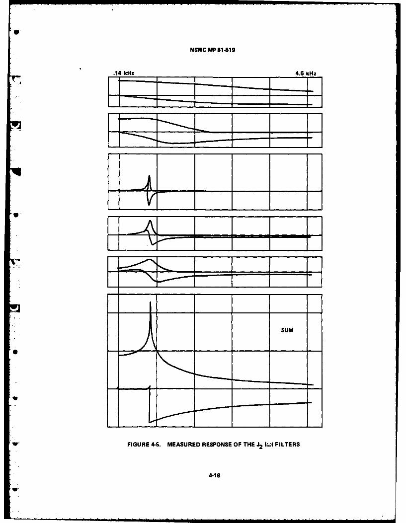
NSWC MP81.19
.14 kHz 4.6 kHz
SUM
0
FIGURE 4-6. MEASURED RESPONSE OF THE J2 (el FILTERS
4-18
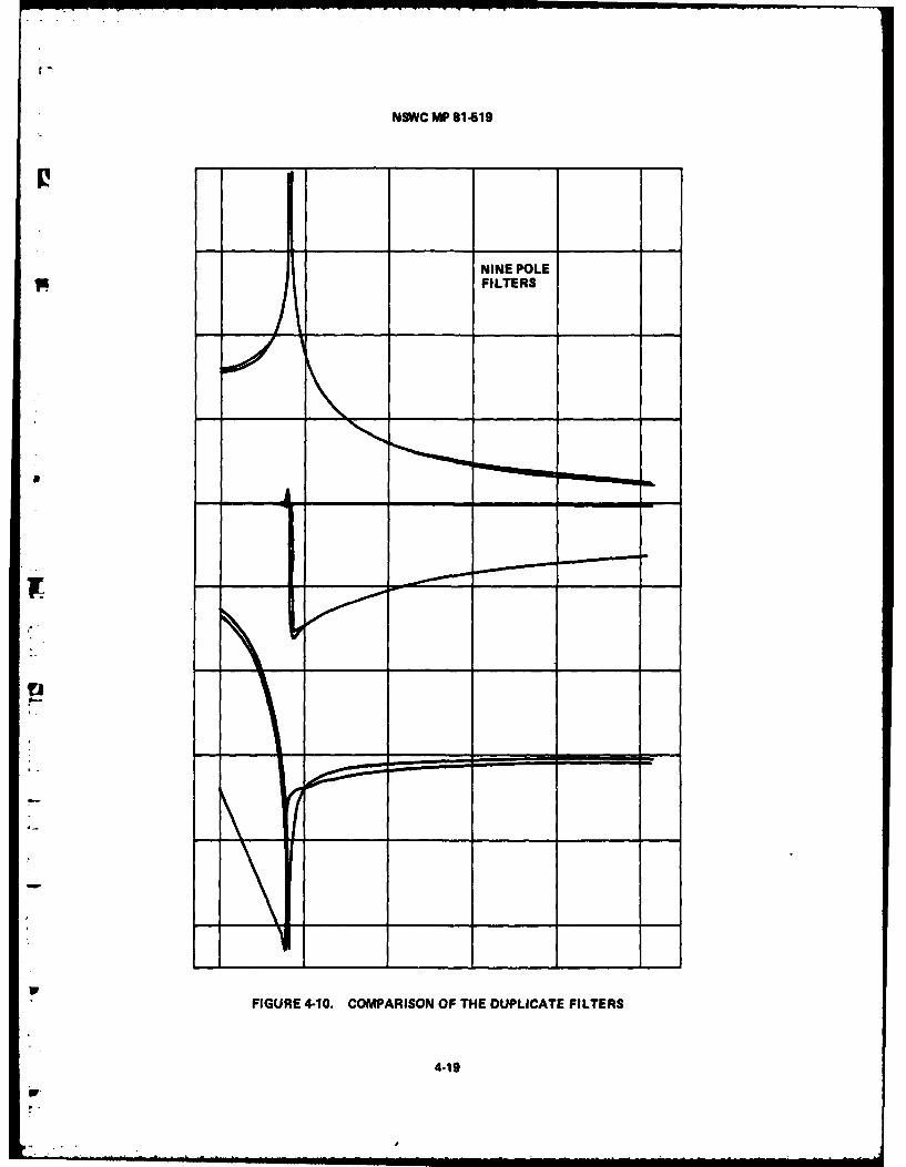
NSWC MP 81419
NINE POLEFILTERS
FIGURE 4-10. COMPARISON OF THE DUPLICATE FILTERS
4-19

NSWC MP 81-519
4.5 Signs
Before discussing the results obtained using the analogue, a brief word
about signs is in order. The literature is full of discrepancies concerning the
sign conventions for J (w) and J (w). Harris has discussed this in.8
detail. aIn the analogue, the signs largely take care of themselves. The
filters in the analogue will always satisfy causality requirements, and the
signs adjust themselves accordingly. it is not possible for the designer to
influence the sign relation between the real and imaginary part of J1()and
J w) hat signs one uses in describing these functions depends largely on
convention. However, the designer can add an overall sign change to either or
*both J(W) and J 2 (wI). This will affect both the real and imaginary
parts of each function. Changing the sign of J 1(w) will make the
quasiparticle resistance look negative instead of positive, an obviously
unphysical situation. The overall sign of J 2 M, however, has no effect on
the input/output characteristics of the analogue. It only affects whether the
VCO phase-locks at 0 degrees or 180 degrees with respect to the LO when the
analogue is biased within the zeroth order step.
The sign of Im J 1(w) is usually taken to be positive. This is
consistent with the association of positive current with positive voltage.
Relative to this, and for the sign conventions implied by equation 2-1, the sign
of Em J 2(a,) is negative at frequencies greater than the gap frequency
26/h. At frequencies less than this, the theoretical expression for 13
J 2 (w) is either zero or positive, depending on temperature.
4-20
NSWC MP 81-519
4.6 Results Obtained Using the High Frequency Analogue
Once the prototype was working, results followed quickly. These are
sunmmarized in the figures that follow. Most of the data is in the form of time
averaged current-voltage characteristics, which can be compared directly with
1P characteristics of real junctions. The presented data were chosen to illustrate
the aspects of the Josephson effects that are not included in the RSJ model.
These include the Riedel peak, sub-gap structure, the nonlinear quasiparticle
resistance and its associated reactance, and the cosine phi term.
The results begin with graphs of the time averaged I-V characteristics
measured under current and voltage bias conditions. Certain parts of the
characteristic are not accessible under current bias conditions. The next
figures show how this difficulty can be avoided through the use of a voltage
source and a large series inductance; The shape of the Riedel peak and the
related sub-gap structure are clearly evident. Later figures show the effect of
nonzero source resistance, leakage currents, and shunt capacitance.
There is a brief digression to illustrate a subtle problem connected with
p the use of the nine point T - 0 filters. This is followed by a series of I-V
characteristics showing the effects of RP currents and voltages.
Some measurements of the AC impedance of the junction are shown for both
* the RSJ and high frequency limits of the analogue (i.e., with and without the
* filters connected). After this are some measurements of the impedance
associated with the plasma resonance. These illustrate the effects of Re
3 (w) and Im J(W on the resonant response.
The behavior of the analogue can be summarized in a few paragraphs. First,
the analogue seems to do a good job of modelling gap effects. The appearance of
sub-gap structure is consistent with predicted behavior, in that it appears only
4-21

NSWC MP 81-519
at odd submultiples of the gap voltage for a current biased junction. 2,5 For
a suitable choice of source impedance, structure is observed at even
submultiples as well.
The qualitative performance of the analogue in modelling nonlinear
quasiparticle tunnelling is good. But there is a problem associated with fine
structure in the imaginary part of the response of the J1 () filter. Under
certain conditions, this causes the quasiparticle resistance to appear
negative. The problem can be avoided at a cost of decreasing the resistance at
voltages below the gap. (This is discussed further in section 8.7.)
The accuracy of this version of the analogue was not sufficient to permit
good quantitative measurements of small signal effects, such as the plasma
resonance. Although qualitative resuls were good, the numbers did not come out
as they should. Part of this can be blamed on the unwanted cosine phi term
introduced by the low pass filters. A combination of noise problems,
particularly in the VCO, and calculation errors by the six multiplier chips is
responsible for much of the additional error. These faults were subsequently
improved in a later version of the analogue. (This is discussed in Chapter 8.)
However, the results presented on the following pages are the first of their
kind, and represent a significant step in the development of the improved
analogue discussed in subsequent chapters. Furthermore, these results do
provide some insight into the complexities of the high frequency theory of
Josephson tunnelling.
* Figure 4-11 shows I-V characteristics for the analogue under current and
voltage bias conditions (cf. Fig. 2-6). Under current bias conditions, negative
resistance regions in the characteristic are inaccessible, and hysteresis in
evident. Note the similarity between the voltage biased characteristic and theW
filter response Im 1 (W).
4-22

I.I
NSWC MP 81-519
AI>
14)
wz44I-j
00
4-??
U
cc
G32
z4ccw
or4

NSWC MP 81-519
To investigate the nature of the Riedel peak, the analogue was connected to
a voltage source via a large inductance. This serves to make the analogue look
voltage biased at DC, and current biased at AC. Figure 4-12 shows the results
for two values of L. Note that the back of the Riedel peak is now accessible
and that sub-gap structure is evident. The Riedel peak in Figure 4-12a is
surprisingly broad. This effect was later traced to the existence of negative
resistance oscillations, which result from the presence of the large source
inductance. This is discussed in section 9.5.
In Figure 4-12b, sub-gap structure appears only at odd submultiples of the
gap voltage 24/e. This is consistent with theoretical predictions.2'5
Figure 4-13a shows the effect of adding a resistance in series with the
voltage source and inductor. The gap hysteresis is still there, but the finite
source resistance causes the hysteretic segments to have negative slope. Figure
4-13b shovs the effect of reducing the shunt resistance from that predicted by
the I.%~ product. This reduces the effective AC source impedance, thus
eliminating much of the gap hysteresis. (There is no resistance in series with
the voltage source in Figure 4-13b.)
The inductor is removed for the measurement shown in Figure 4-14, in which
the analogue is connected to the voltage source through different values of
series resistance. Note the transition from voltage bias to current bias.
Figure 4-15 shows the opposite effect. The analogue is connected to a current
source, and the shunt resistance is varied. In 4-15a, the shunt resistance is
that given by the I, product. As this resistance is decreased, the
hysteresis diminishes, and the junction begins to look RSJ like.
Figures 4-16 and 4-17 are a closer examination of the effects of voltage
biasing the analogue throuqh a series inductance. As the inductance is
4-24

I4SWC MP 81-619
pc
10
4-25
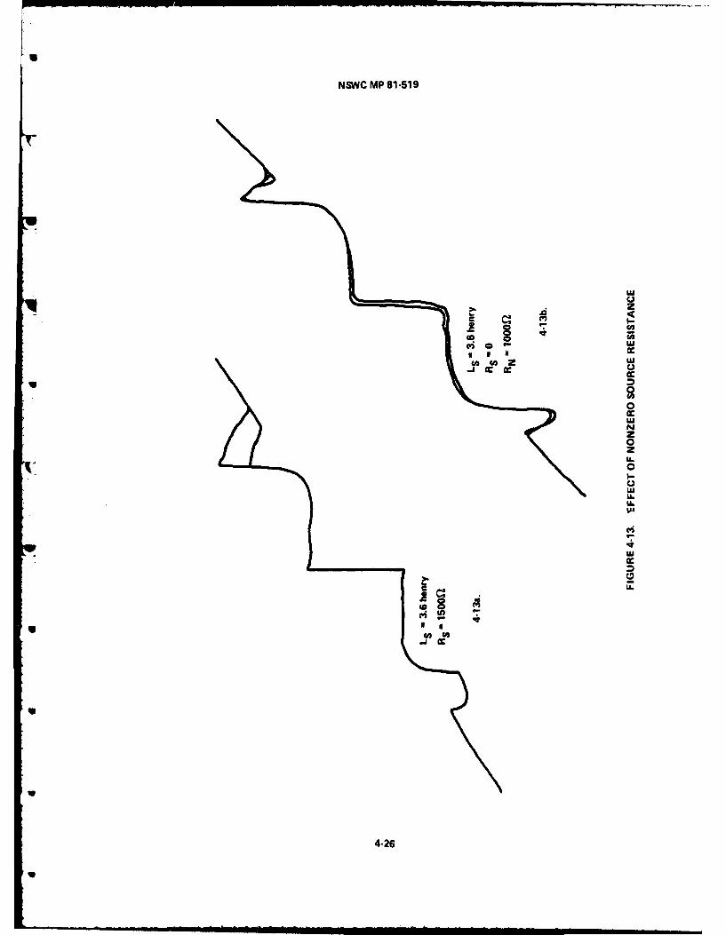
NSWC MP 81-519
LU
'UN
Uz
0
0
ILWI-
'U
LoL
cq -i
no 10
4-26
-18753 ELECTRONIC SIMULATION OF THE JOSEPHSON EFFECTS(U) NAVAL 2/4SURFACE WEAPONS'CENTER SILVER SPRING MD D JABLONSKIBi DEC Bi NSWC/MP-8l-519 SBI-AD-F598 877
UNCLASSIFIED F/C 28/IS N
smhhhhhhhhhllsmhhhhhhhhhhhlomhhhmhhhhhhEhhhhhhhmhhhlmsomhhhmhhhhhusmhmhhhhhhhlo'Ehm1h 10i imonsmoon

IIIII11.0 1" W a"8*hIIm 3M13
11111 ii 1 2II
11112 1 1 .- 6 6
MICROCOPY RESOLUTION TEST CHARTMICROCOPY RESOLUTION TEST CHART t NATIONAL BUREAU OF STANDAROS-1963-A
NATIONAL BUREAU OF STANDARDS-1963-A
W Q2
lilll ,__1,6
111111 11114 11.II III 12 IIIl .4 ll1.
MICROCOPY RESOLUTION TEST CHART'_. - NATIONAL BUREAU OF STANDARDS-1963-A r -
W4 12 2 1L.2- 6 L
II1!.25 1. 1 .
/
MICROCOPY RESOLUTION TEST CHART MICROCOPY RESOLUTION TEST CHARTNATIONAL BUREAU OF STANOARDS-1963-A NATIONAL BUREAU Of STANDANOW-1963-A
-. /

NOW MP $1419
ICz IL
I
4-27
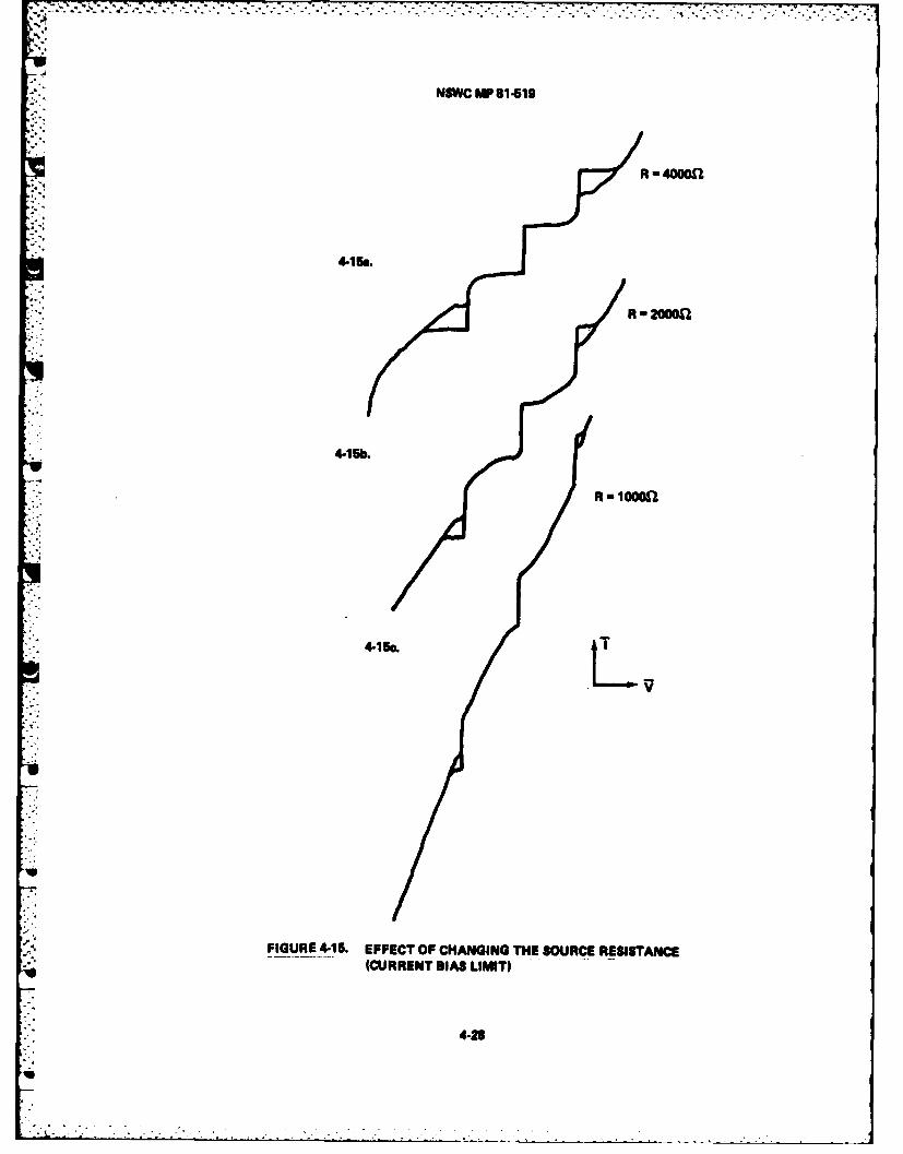
NSWC MPD 81419
Ru 4000nl
4-15s.
R -2000f
4-15b.
FIGURE 4-15. EFFECT OF CH4ANGING THE SOURCE RESI8TANCE(CURRENT BIAS LIMIT)
4-28

NC HP 61619
I V6
- ul
fs17.
4-29

NIWC MP8I619
(4 I~bU I
'a,
I-
3wz
I
IE
~1 Uaa
a IIS.
wU
SI.SI.mu
mug
U
U7-F-
440

NSWC MP 81-519
increased, the characteristic approaches that of the current biased case. Note
p that the sub-gap structure occurs only at odd submnultiples of the gap voltage,
and that the Riedel peak gradually broadens (cf. section 9.5).
Figure 4-18 shows the effect of adding a shunt capacitance to the analogue,
which Is still voltage biased through an inductor. The AC equivalent circuit is
an IW network in parallel with the analogue. This cavity apparently causes
structure to appear at even submultiples of the gap voltage. This is consistent
with the predictions of Werthamer and Harris.2'5
L-' Figure 4-19 illustrates the effects of shunt capacitance on the DC I-V
characteristics of a current biased analogue. Results are shown for the
analogue operating in both the RSJ and high frequency modes. The amount of
.. hysteresis depends on the RC product, In the high frequency case, the value of
.4 R to be used is that of the differential resistance at V = 0. In the figure@
this is approximately ten times as large as RM. Thus, for a given amont of
hysteresis, only one tenth the capacitance is needed as in the RI case. The
large amount of hysteresis is typical of that observed in a real superconducti
tunnel junction.
When using the analogue with the nine pole T - 0 filters, unrealistic
behavior was observed when there was a shunt capacitance and a high source
impedance. This is shown in Figure 4-20. The characteristics of the current
biased and voltage biased analogue are superimposed. Under current bias
conditions, the I-V curve enters a negative resistance region. That is, the
curve enters the second and fourth quadrants of the I-V plans, and the I-V6w'
product Is negative. This unrealistic effect was traced to the overshoot in the
Im J1 (w) filter response at the gap frequency. The overshoot is apparent in
4-31

%A ~ - - . -~ - . -. . - -
2
NSWCMPS1-519
* 4 U U Iill
o 0Iii. Ig
muU
U U-'U
3ii -Imur1~~ -'
U U-'U
a.a
12UmuiU
I~h 'a.0
Ii'I.U.mu
mu
U.U..
U.
432

NSWC MPSM1519
II
S *0
IIuj UU
0t-
AAlMI
icU
U 4-3

NSWC MP $1419
1>IIc
z
* ci4--c
Ucc
4-34

;., "" " -" -'..Y . -.i . - . .i. . . .. -"-,- - . - . . . --- ..- . --- -- " - " . i " "
NSWC MP 81-519
the voltage bias curve of 4-20b at the gap voltage 2A/e. Before making
if measurements with the capacitively shunted analogue, the shunt resistance was
decreased until the I-V characteristic looked realistic from an energy
conservation point of view. This is illustrated in Figure 4-20a. Note that the
*current biased curve starts behaving properly when % is adjusted to lift the
overshoot in the voltage biased curve to just above the axis. In the time
domain, this overshoot shows up as a voltage source at the gap frequency. If
the shunt capacitance is sufficient to make the plasma frequency approach the
gap frequency, the analogue will oscillate. The oscillations disappear when the
shunt resistance is decreased, or the capacitance is removed. For most
measurements not involving capacitance, the shunt resistance was set to satisfy
the IoN product. For measurements using a capacitor, R was decreased
* sufficiently to get rid of the problem. This usually meant lowering R% from
1500 to 1200 ohms. It may be that the overshoot in lu J11(1 is responsible
for the apparent structure at half the gap voltage in Figure 4-12a. A .agative
resistance at the gap frequency might generate oscillations at half that
frequency, resulting in the observed structure. As the source impedance is
*decreased, the structure goes away.
Figure 4-21 shows the I-V characteristics for an assortment of RC
products. The IORj product is less than wA/2e for all four curves, so the
'- problem described above is avoided. Note the structure in the excess currents
below the gap voltage in Figure 4-21b. This is the sort of behavior seen in a
- real junction. There has been some controversy as to whether it is caused by
multiparticle tunnelling, which is not modeled by the analogue, or self-coupling
effects, which are.38
4-35

N 7
NSWC MP 81419
I.-
0IL
Oa.
IWU
1>=
r40
4-36.

NSWC MP 81-519
The next few figures show the effects of microwaves. Figures 4-22 and 4-23
show characteristics for the current biased analogue with the drive frequency at
the gap frequency and half the gap frequency, respectively. As the RF amplitude
is increased, the characteristics get washed out. Much of this effect can be
I ~ attributed to the existence of the photon-assisted tunnelling (PAT) steps, which
interfere with the Josephson steps and smear the characteristic. A discussion
of this, along with quantitative measurements, is included in Chapter 9.
Figure 4-24 shows the effect of varying the drive frequency while holding
Kthe amplitude of the drive current constant. There seen to be some spurious
effects in curve a, but the spacing between steps is correct.
Figure 4-25 was obtained by varying the source resistance. The gradual
change from current spikes to current steps, and the disappearance of gap
hysteresis, Is well illustrated.
Figure 4-26 shows the effect of driving the analogue at frequencies just
above and below the gap frequency. There appears to be some spurious behavior.
The next several pages deal with the AC impedance of the analogue. The
measurements are similar to those described in Chapter 3 for the MSJ model.
Figures 4-27 and 4-28 show result. obtained using the analogue in both the RBJ
and high frequency modes (i.e., with and without the filters connected). Note
that the impedance curves for the high frequency case are not symmetric with
K. respect to positive and negative current, because of the hysteresis (apparently
RF induced) in the I-v characteristic. The current is swept in only one
I direction for the impeance measurement, which would otherwise appear
hysteretic. In the RSJ limit, the reactance of the analogue should be zero
between steps. This Is not quite the case when the analogue is operated in the
RSJ mode, and Is probably due to cumulative multiplier error. However, in the
4-37

NSWC MP 81-519
wL
* ..
4-M-

NSWC MP 81419
UU
UU
4-39

NSWC MP 81419
U 4
q
U
U.
g
4
zU
IL0I-U
N muz IA.
muA U.4 N
4muU
U.
I4
A4
U
4.40
q
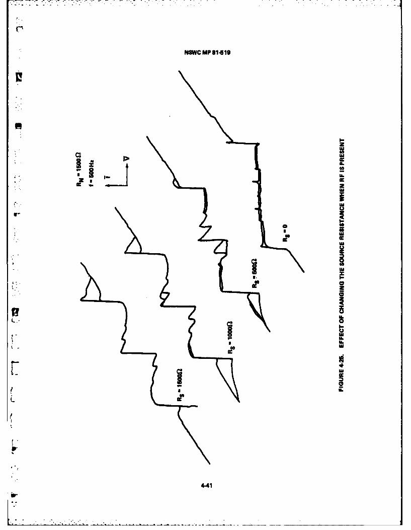
r
NSWCMPS1619
I-z
a.4~
ZE2w
SMU
aUI, SM
* U
SM
* I I0U
* 2
pI-
U57~ I I0- 4
SML.I 'I.UL
=
4.41
p.

NSWC MP 81-519
z
U.
1>1
4-42

NUVC MP 1619
RESISTANCE
IDC
REATANE RECT E
IR
FGRES27 IGHAEUECIMDAE
4-43

NSWC MP 81419
'DC
REACTANCE
DIRECTION OFCURRENT SWEEP
RESISTANCE
w -~ DC
'-CREACTANCE
WERTHAMER
FIGURE 4.28. HIGH FREQUENCY IMPEDANCE (CONTINUED)
44
NSWC MP 81-519
high frequency mode, one would expect Re JI(w) to contribute a reactive term
between steps. It in interesting to note that in Figure 4-28b, the reactance is
negative in the zeroth order step. This is a consequence of the large
difference in the quasiparticle resistance between the RSJ and Werthamer limits
when 0 a .4. This is discussed in section 9.2.
The last few figures deal with the plasma resonance. The capacitively
shunted analogue is current biased within the zeroth order step. For small I
currents, the analogue will look like a parallel RCL network, with resonant
frequency given by equation 2-32. The Q of .this resonance is affected by the
sign and magnitude of the coo* term. To investigate this, efforts were made
to measure the Q under a variety of conditions. However, the quantitative
interpretation Is complicated since, in the region of interest, the extraneous
cos term introduced by the low pass filters can be significant. As a
Lresult, the measured Q was often larger than it should have been, as thenegative cos# term increased the effective resistance of the analogue.
However, the dependence of the plasma frequency on cos (cf. Eq. 2-32), was
quite well followed. And for small input signals, the resonance was clearly
Lorentsian.
1? For the first five figures, the analogue was operated in the RS mode. The
figures show the real and imaginary parts of the impedance of the capacitively
[1" shunted analogue as a function of frequency. The measurement technique is
[4
4-45
* .
NSWC MP 81-519
identical with that used for previous impedance measurements, except that the DC
bias current is held constant, and the frequency varied. Figure 4-29 shows a
typical resonance for several values of PF input current. The resonant peaks,
as veil as the half power points, are at approximately the same frequencies
independent of current amplitude. The amplitude of the resonance varies
linearly with the amplitude of the input current.
Figure 4-30 shows the impedance for several values of DC bias current. The
plasma frequency changes in the appropriate manner, and the Q follows the
expected behavior to a reasonable degree. Figure 4-31 is a plot of f /Q versusp
f for a series of measurements. If the coo# term is xero, f /Q should bep p
uconstant, and all of the points should fall on the line given by (2*RW)-
The scatter in the data points is reproducible, which Indicates a frequency
dependent source of error in the analogue. Investigation suggests that
multiplier inaccuracy is partly to blame. Other measurements similar to those
of Figure 4-31 were made, but they were considerably less consistent with
theory. Attempts to make quantitative measurements using the analogue In the
high frequency mode were abandoned until the necessary improvements were made to
the circuitry. The resulting quantitative data are presented in Chapter 9.
However, the simple qualitative results presented here illustrate the effects of
S1W) and J2(w). Figure 4-32 shows the plasma resonance for a frequency
less than the gap frequency. The top curves are for the RSJ limit. The second
set of curves are with the J(W) filters connected. This causes some
structure at the gap frequency, but the Q is not greatly affected. The third
set of curves are for the analogue with both J 1 (w) and J 2(W connected.
The dramatic increase in Q is a result of the high quesiparticle resistance at
voltages below the gap. The decrease in resonant frequency is due to the
inductance of Re J1W (cf. Section 2.6).
4-46

NSWC MP 81419
ImUUw0
up7
Uc
4-47

NSWC MP 81-519
IIa I
wa
z. z
4-48)
La

NMWC MP 81419
II
(00
( leg
El
4-49

NSWC MP 81 .519
J2 W1 ON, J, (W) OFF
C 220dfop 1000 Hz
C- R 12soo
U SINO .- 0
FIGURE 4-32. PLASMA RESONANCE (HIGH FREO ANALOGUE)
4.50

NSWC MP 81-519
The measurements illustrated in Figure 4-33 are identical to those of
. Figure 4-32, except that the plasma frequency is greater than the gap
frequency. The top curves, for the RSJ limit, are reasonably Lorentzian. As in
Figure 4-32, the effect of connecting the Jl(W) filters is to lower the
resonant frequency. However, the Q is not raised dramatically, as the Jl(W)
filter has little influence on the resistance of the analogue above the gap
frequency. In Figure 4-33b, the large negative amplitude of Im J 2(w) above
the gap frequency seems to increase the Q slightly.
Figures 4-34 and 4-35 show the effect of increasing the amplitude of the
RF input to the analogue when operated in the RSJ mode. As expected, the curves
0- begin to look very non-Lorentzian.
4.7 Summary
The discussion and results presented in this and the previous chapters
represent an overview of the design of the original versions of the high
[ frequency analogue. The results have demonstrated that aldram's scheme for
modelling the high frequency theory is not only feasible, but practical as
well. Inspired by this, further improvements were made to the analogue, and
[f! experiments were repeated in a quantitative, as opposed to qualitative, manner.The next several chapters describe this work, beginning with additional
discussion of the high frequency theory. This is followed by a description of
how the analogue has been improved, and, a summary of the numerous additional
t results that have been obtained.
4
4-51

NSWC MP 81 -519
RSJ
J2ON, J, W~ DISCONNECTED
BOTH J1 (w) AND J2f W CONNECTED
w 600Hz5600 Hz
C .022;Ed fgpm1000HzRN - 1800S2
SINO-
FIGURE 4-33. PLASMA RESONANCE (HIGH FREQ ANALOGUE, CONTINUED)
4-52

ir
NSWC MP 81-619
N o
*MUZ
I
L-J
U.
a
cc-
4-53I Ii
a
, .'
''U,1oU
r" " 2

NSWC MP 81.519
cc (i
~L
.~IC
* liZ
LU
zZ
C4
t U.
I-
LU
4-54
NSWC MP 81-519
CHAPTER 5
DISCUSSION OF THE HIGH FREQUENCY THEORY
5.1 Introduction
In Chapter 2, the high frequency theory developed by Werthamer was
discussed in very pragmatic trms, with little attention given to the
underlying physics. In this section we elaborate on the earlier discussion
by calling attention to the various assumptions implicit in the theory,
and also to the strengths and weakniesses of the theory. An the basics of
the RSJ and Werthamer models have already been discussed, this section is
relatively informal. It is designed to stress points that have not been
discussed earlier, and is not a complete, self-contained discussion of the
theory.
5.2 Josephson's Calculation
Prior to Josephson'. work, it was believed that multiparticle
tunnelling between two superconducting electrodes could occur.* However,
it was assumed that such tunnelling would be highly improbable, and thus
unobservable, compared to single particle tunnelling. For example, if the
current due to single particle tunnelling is proportional to the square
of a matrix element, T 2, the current due to events in which two electrons
tunnel simultaneously would be expected to be proportional to T . This was
based on the assumption that the simultaneous transfer of two electrons
was an incoherent process, and that its probability was proportional to the
product of the probabilities of the separate one electron transfers.1 1
Josephson demonstrated the existence of a coherent process in which
two electrons tunnel simultaneously. This process has an effective matrix
2element proportional to T ,but since it is coherent, the tunnel current
5-1

NSWC MP 81-519
is proportional to the effective matrix element, and not to its square. The
2current is thus proportional to T , as in single particle tunnelling. This
process is illustrated in Figure 5-1. (In the various sketches, the
possible contributions to the tunnel current are shown with respect to the
Bose condensate of paired electrons at the Fermi en~ergy, and the bands of
excited quasiparticle states above the Fermi energy.) Figure 5-la shows
the transfer of a single excitation across the barrier. This particular
process will occur only at finite temperature, as it relies on the
existence of occupied states above the Fermi level. This process is
proportional to T2
Figure 5-lb illustrates a multiparticle tunnelling event in which
two excitations cross the barrier simultaneously. This is shown in
terms of a virtual state, which is a convenient way of illustrating the
intermediate state that arises in the perturbation theory used to describe
the event. The tunnel current for the process in Figure 5-lb is proportional to
4T , as the two electrons tunnel incoherently. This process also occurs
only at finite temp~erature.
Figure 5-lc shows the pair tunnelling process predicted by Josephson.7
In this case, two electrons from the condensate cross the barrier
coherently, resulting in a contribution to the current proportional to
2 4T , not T . Note that this process occurs at zero voltage. This is the
DC Josephson effect. (As before, the virtual state is a means of
illustrating certain aspects of the perturbation theory used to describe
the transition.) The DC Josephson effect can occur at zero temperature.
The next few sketches show other tunnelling events that are of
interest. Figure 5-ld shows how breakinq a Cooper pair can result in the transfer
5-2

NSWC MP 81-519
5.1a 5-1(b)
2,. .2 A2Al' AI TI-,
;.QUASlPARTICLE TUNNELING MULTIPARTICLE TUNNELING
*AT FINITE TEMPERATURE
5-1(s) 5-1(d)
; '1 A 2 A
eV
QUASIPARTICLE TUNNEUNG AS As~l(, L sill)RESULT OF PAIR BREAKINGAA2
C P FCV 0
V PHOTON-ASSISTED TUNNE LING 1 CV
MULTIPARTICLE TUNNELING
IA 2 2
AC JOSEPHSON EFF=CT
FIGURE 5-1 TUNNELING PROCESSES IN JOSEPHSON JUNCTIONS
5-3

NSWC MP 81-519
of a single electron across the barrier. Note that for voltages eV < Al + 2 ,
this process will not occur, as sufficient energy is not available. However,
with the addition of a photon (or phonon), this process can happen, as
shown in 5-le. Figure 5-lf shows an example of an energy conserving
multiparticle tunnelling event. The energy gained by the transfer of a
pair across the barrier is sufficient to break another pair and form two
quasiparticle excitations, one on either side of the barrier. This process
2is of much higher order than T . As processes such as these are highly
improbable, Josephson neglected them in his calculation. The last sketch,
Figure 5-1g, shows the transfer of a Cooper pair as in Figure 5-1c, but
for nonzero voltage. Note that a photon of energy hf = 2eV is emitted.
This is the AC Josephson effect.
Various aspects of the Josephson effects will be discussed in more
detail in connection with the Werthamer theory. At this point, it is
worth discussing more completely some of the assmptions implicit in
Josephson's original work.
First, in his original calculation, Josephson required that the
voltage across the tunnel junction be constant, or at most slowly varying.
This meant that the phase difference could be defined very simply by
* - 2wft, where f is the Josephson frequency 2eV/h. This greatly
simplified his calculation, but eliminated riany interesting aspects of the
li problem.
Second, Josephson chose a situation in which higher order processes,
such as the multiparticle tunnelling inFigures 5-lb and 5-1f, would be negligible
with respect to the single electron and coherent pair processes. On the
other hand, these latter events were assumed to be highly probable, yet
5-4

NSWC MP 81-519
describable in terms of simple perturbation theory. In a real situation, this
corresponds to a tunnel junction where the barrier is neither too wide
(no tunnelling probable) nor too narrow (higher order processes probable).
That this situation is reasonable can be seen from the following argument.
Simple quantum tunnelling through a barrier can be described by an
expression I - A exp(-x/B), where x is the barrier thickness and B is
related to the barrier height. For a typical situation, this transmission
coefficient can be approximated by exp (-x/Angstrom), or exp (-x), where x
is in Angstroms. A higher order, oultiparticle tunnelling current wouldF-
be proportional to exp (-2x). For x on the order of an Angstrom, exp (-x)
and exp(-2x) are comparable in magnitude. However, for x - 10, the
transmission coefficient is large enough that exp (-x) describes an
observable current, is small enough that this current can be described as
a small perturbation, and is such that terms proportional to exp(-2x) can be
completely neglected. Barrier thicknesses of this size are what one
Nachieves if the barrier is formed by natural means, such as letting a thin
film of superconductor oxidize in a room atmosphere until reaching
equilibrium.
In an actual tunnel junction, one can be reasonably confident that
multiparticle effects are small, if not negligible. If multiparticle
effects were a major contribution to the tunnel current, the total current
would be in significant disagreement with the current predicted by the I A
product deduced by Josephson, and this turns out not to be the case. On the
other hand, it is sometimes likely that a tunnel junction will have -pots
where the tunnel barrier is locally much thinner than for the rest of the
Junction. This permits some multiparticle tunnelling to occur, but in5-5

NSWC MP 81-519
amounts small enough not to make the total current behave in an
un-Josephsonlike manner. Such locally thin regions are found in junctions
made using simple evaporation and oxidation techniques, where pinholes in
the barrier are common. However, state-of-the-art techniques permit: i 13
fabrication of junctions that show no sign of multiparticle effects, and
Josephson's original assumptions are well established as to their validity.
In making the assumption that the junction voltage was constant,
Josephson greatly simplified his calculations. By making the further
assumption that the voltage was small compared to the gap voltage of the
*" superconductor (which in the voltage bias limit corresponds to saying the
current, as well as the voltage, is slowly varying), Josephson was able to
treat quantities such as the critical current and junction voltage as being
constant. This assumption allows one to ignore much of the BCS theory
once the calculation is complete. For example, the RSJ model contains no
direct reference to temperature or the superconducting energy gap.
Lastly, Josephson worked completely within the framework of the BCS
theory. With respect to the RSJ model, any corrections to BCS (to take
into account strong coupling effects, for instance) would be reflected
*primarily in an adjustment of the IJRN product.
5.3 The Werthamer Theory
Simply put, the Werthamer theory is a repeat of Josephson's calculation,
but with no simplifying assumptions made about the magnitudes or
frequencies of the junction voltage and current. 5 The assumptions about
higher order effects and validity of perturbation theory are the same, and
V the calculation is done within the confines of the BCS theory. The
5-6

NSWC MP 81-519
differences between Josephson's first calculation and the Werthamer theory
are well seen by examing the differences between the block diagram of the
RSJ analogue (Figure 5-2a) and that of the high frequency analogue (Figure
5-2b). Note that the RSJ analogue contains only a sine term (no cosine
term, except for the extraneous contribution caused by the unwanted
phase shift of the low pass filter), and that the temperature and frequency
dependent response functions J and J2 are either ignored or treated as
being constant.
It might be well to note that J and J represent spectral responseF1 2
functions, which contain all of the information about the quantum response
of a tunnel junction to an applied current or voltage. The use of the
functions 1 and J2 allows for a classical model of a quantum phenomenon
(e.g., the filters in the electronic analogue model quantum behavior in
a classical way).
Figure 5-3 illustrates some of the important aspects of the Werthamer
theory in more detail. Figure 5-3a shows the transfer of a single excitation
via a pair splitting process at eV - A1 + A . As mentioned before, this
process will not occur for voltages less than eV - A1 + A 2 . However, due to
- the singularities in the densities of states at the gap edge, the onset of" this current at eV A A + A will be extremely rapid. This accounts for the
1 2* sharp knee observed in the quasiparticle current of a tunnel junction at the
gap voltage (cf. Figure 5-3b). For T > 0, there will also be excitations
of the form diagrammed in Figure 5-la, resulting in quasiparticle current
at voltages less than the gap voltage.
The singularity in the density of states is also reflected in the
Riedel peak in the supercurrent at the gap voltage for a current biased
5-74'

NSWC mP 81-519
5-2a THE RSJ ANALOGUE (AFTER BAK AND PEDERSEN) 4
i VCO VOLTAGE CONTROLLED OSCILLATORLO LOCAL OSCILLATOR
PS PHASE SHIFTERVCCS VOLTAGE CONTROLLED CURRENTSOURCE
W LPF LOW PASFILTERV IN V ER TER
::+ ADDER
SCCFIUE5-2 LC IRMO THE HIH REUEC ANALOGUE(ATRBKNDPESN4
-- FIGURE 52. THE RSJ AND HIGHFREQUENCY ANALOGUES
;Q 5-8
cc /
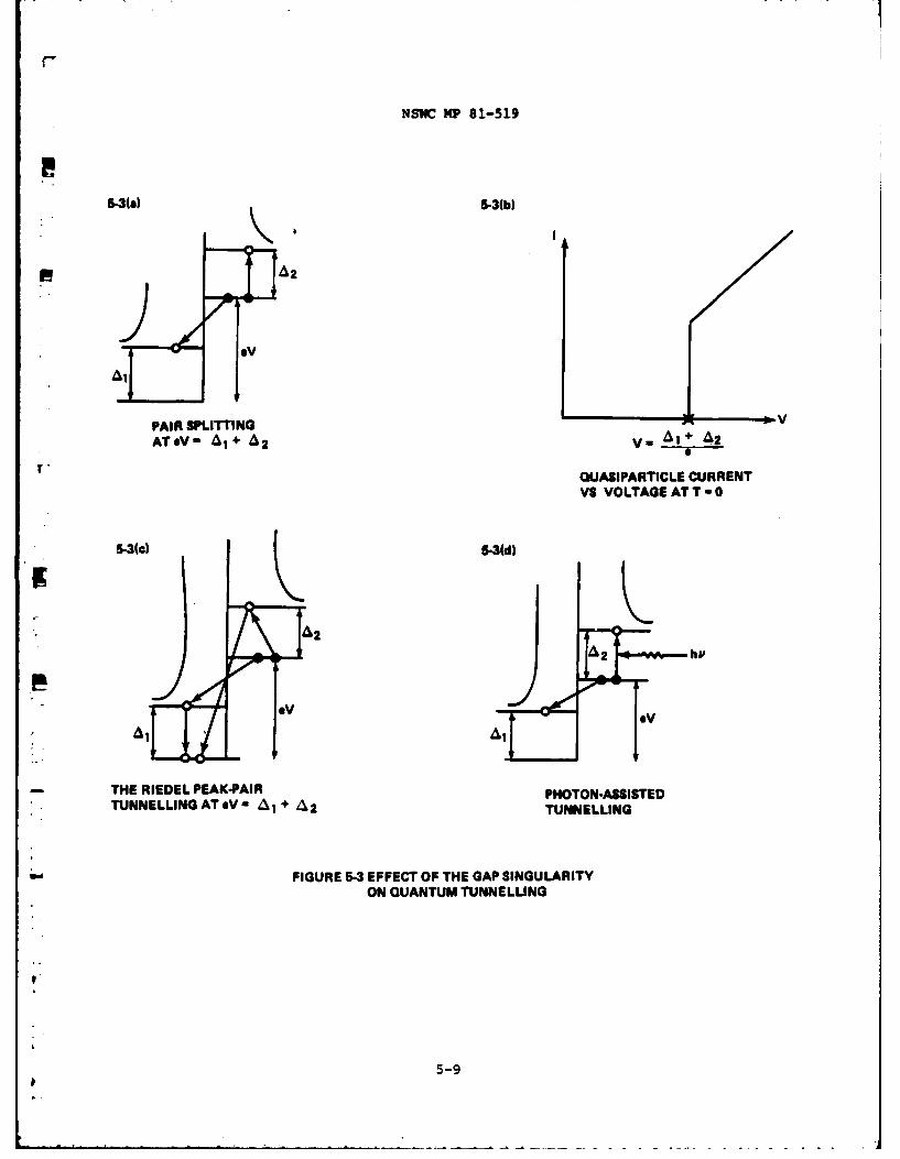
r
NSWC MP 81-519
5-31ol 5-3(b)
PAIR SPLITTING -
AT.V" A 1+ & 2 V- &1
+ 12
OUASIPARTICLE CURRENTVS VOLTAGE AT T -0
-3(0) 5-3(d)
A2
A2 hp'
V iV
THE RIEDEL PEAK-PAIR PHOTON-ASSISTEDTUNNELLING AT V- A I + A 2 TUNNELLING
FIGURE 5-3 EFFECT OF THE GAP SINGULARITYON QUANTUM TUNNELLING
5-9
V
NSWC MP 81-519
tunnel junction. This is sketched in Figure 5-3c. The supercurrent is
represented by the transfer of a pair across the barrier via an intermediate
state. In second order perturbation theory, the probability of this transfer
is proportional to the inverse of the difference between the energy of the
original state and that of the intermediate state. For a given bias level,
the probability is dominated by the intermediate state contribt,'ions in which
the difference between these two energies is at or near zero. When
eV - AI + A2, the intermediate state for which the energy difference
is zero can coincide with the singularity in the density of states at the gap
edge. The Riedel peak in the supercurrent at eV - A1 + a2 arises from
this coincidence.
Figure 5-3d shows a single excitation crossing the barrier for a voltage
eV less than A + a 2. The extra energy required to break a pair is
provided by a photon. In the sketch, the photon has just enough energy to
create excitations at the edge of the excitation spectrum, where the density
of states is singular. In this case the photon must provide energy
hv = (A1 - eV) + A2
This photon-assisted tunnelling causes steps to appear in the time-
averaged I-V characteristic of the junction at the voltages
eV - A1 +a2 + nhv (5-2)
where n is an interger.
At this point we can discuss the existence of structure at submultiples
of the energy gap voltage (A1 + a2 )/e. If the photon assisted
5-10

NSWC MP 81-519
tunnelling described above is caused by the feedback of current at
multiples of the Josephson frequency from the source impedance, as opposed
to being provided externally by photons of arbitrary frequency, then
there will be a relationship between the energy of the photons and the
bias voltage. This results in the presence of various structure in the5
time-averaged current-voltage characteristic of the junction. For
example, if the junction is biased through a finite source impedance at an
average value eV, then photons will be available at all multiples of the
Josephson frequency hfj - 2eV. (Strictly speaking, DC supercurrent can
only exist when the source impedance is nonzero. In the constant voltage
limit, there is no time average supercurrent, and the effects we are
discussing will not be apparent in the DC I-V characteristic.) These
photons can contribute to additional pair splitting, and at certain bias
levels this effect is enhanced by the singularity in the density of
states at the gap edge.
For example, Figure 5-4a shows a photon of energy hf (generated by the
transfer of a pair across the barrier as in Figure 5-1g) being fed back to the
junction via a complex interaction with the source impedance. If the bias
voltage is such that the energy hf is just enough to split a pair andJ
create excitations at the gap edge, then this feedback effect will be
enhanced by the singularity at the gap edge. That is, when
hf A - eV+A 2 (5-3)
When the pair recombines, a rhoton must be emitted with energy mhfj
(m is an integer) such that
5-11

NSWC MP 81-519
5-4a
GENERATION OFa+ASUB-GAP STRUCTURE AT eV
1/1/
1.0
11.0
0.
0.5m 1.0 1.5 2.0. 1__ _ _
V R/RN 20
5-4b ODD SUB-GAP STRUCTURE VIN A CUR RENT-BIASED 5-4c EXAMPLE OF EVENTUNNE L JUNCTION SUB-GAP STRUCTURE(A FTE R MCDONA LD, ET A L) 2 DUE TO THE PRESENCE
W OF A MATTIS-BARDEENSUPERCONDUCTING LOAD
(AFTER MCDONALD, ET. AL.) 2L. FIGURE 5-4 SUB-GAP STRUCTURE
5-1

r
NSWC MP 81-519
mhfj - hfj + 2eV (5-4)
Since hfj - 2eV, we have m - 2. In the general case, the splitting
of a pair with a photon of energy hf is enhanced by the gap singularity
whenever
nhfj - 1 + A2 - eV (5-5a)
or
eV - (AI + A2 )/(2n + 1) (5-5b)
The emitted photon has an energy
mhfj - nhf + 2ev (5-5c)
or
m- n + 1 (5-5d)
For the case where n - 0, we have the Riedel peak at eV -1 + A2. For
n > 0, we see "images" of the Riedel peak at sub-gap voltages given by
eV - (Al + a )/(2n + 1) (5-5e)1 2
For a current biased junction, this odd series shows up as extra
structure in the time-averaged I-V characteristic (cf. Fig. 5-4b). This
feedback of Josephson photons back to the junction via the source
39impedance is sometimes referred to as "frequency dependent self-coupling".
An additional effect which is of interest occurs at even submultiples
of the gap voltage 2A/h. In this case, currents at multiples of the
p- Josephson frequency are affected by the sharp rise in the surface impedance5
of the junction electrodes at the gap frequency. This rise, which is
5-13

1-
NSWC MP 81-519
relatively broad compared to the sharp structure associated with the Riedel
peak, shows up in the time-averaged I-V characteristic as broad structure
at the voltages eV - 2A/2n, where n is an integer. In the case of a jumction
comprised of different superconductors, structure appears at voltages
eV = 2A /2n and 2A 2/2n. This broad structure is shown in Figure 5-4c
as calculated for a junction comprised of identical superconductors having
a surface impedance of the type described by Mattis and Bardeen.2
Another process which will yield an odd series of sub-gap structure
can result from higher order, multiparticle tunnelling as shown in
Figure 5-1f. The energy required to split a pair and create two quasi-
particles (one of which crosses the barrier) is generated by the simultaneous
direct transfer of one or more pairs across the barrier. 2,5 This is
enhanced by the gap singularity when
2neV -1 - eV + A2 (5-6a)
or
eV - (A1 + A 2)/(2n + 1) (5-6b)
As discussed earlier, this process is not included in either
* Josephson's or Werthamer's treatment of the tunnelling problem.
One of the shortcomings of the Werthamer theory is that it ignores
non-BCS effects in, for example, lead tunnel junctions, where strong-
* coupling effects are present. Some of these effects can be incorporated
into the Werthamer theory by modifying the functions J and J 2 In the
simplest case, this would mean adjusting these functions so that the I JRN
* product and gap frequency agree with experimental observation.40 Kulik,41
et al. have carried this a step further by modifying the individual
5-14
W-
NSWC MP 81-519
response curves to account for anisotropy and relaxation effects, and the
influence of electrode inhomogeneity.
Another effect which is not included in the Werthamer theory is
phonon-assisted tunnelling. However, this is of little consequence in
junctions comprised of weak-coupling superconductors (e.g., tin), and42
disappears in all types of junctions as T approaches zero.
In any event, deviations from BCS are not expected to change the
basic nature of the frequency, temperature, and voltage dependences described
by Werthamer. Furthermore, in junctions comprised of weak-coupling
superconductors,which are well described by the BCS theory, one would
expect the Werthamer description to be quite good. As for multiparticle
and any anomalous effects, the current experimental situation seems to be
that people are striving to fabricate junctions that conform with the theory,
as opposed to developing more complex theories that describe nonideal
junctions. The conclusion is that for tunnel junctions which are currently
of interest, the theoretical model used by Werthamer is sound, and
represents a substantial improvement over the RSJ model. (As pointed out
in an earlier chapter, other types of weak links, such as microbridges, are
more adequately described by the RSJ model. One would expect that the
theories of microbridges and tunnel junctions might differ substantially,
so this is not necessarily a criticism of the Werthamer formulation.
5.4 Experimental Corroboration of the Werthamer Theory
Surprisingly, there is not a great deal of experimental evidence to
support the finer details of the Werthamer theory. There is also experimental
evidence that is in direct disagreement with it. Most of the difficulty
5-15

NSWC MP 81-519
arises from the presence of the shunt capacitance in a tunnel junction.
This causes the time-averaged current-voltage characteristic to be highly
hysteretic, with the result that most of the structure predicted by the
theory is hidden. For example, the Riedel peak and corresponding sub-gap
structure are completely wiped out for even relatively small values of
shunt capacitance. This is shown in Figure 5-5.2
On the other hand, the presence of the highly nonlinear quasiparticle
curve is clearly demonstrated in the high capacitance limit. In a tunnel
junction, this current is often in good agreement with the prediction that
I approaches Im J1 as the source impedance is lowered. 1 7
The most significant disagreement between theory and experiment seems
to be the question of whether the cosine phi term is positive or negative
with respect to the quasiparticle term in the low frequency, low voltage
limit. 1 Most experimental evidence suggests that the sign of the cos phi
term is negative, whereas the Werthamer theory clearly predicts it will be
positive. 8,9, 43, The interpretation of the experimental evidence has
been done on the basis of the RSJ model with modification to include the
cosine phi term, however. As discussed in the next chapter, this can
lead to important errors in both the qualitative and quantitative
evaluation of the data. However, taking this into account does not
resolve the discrepancy.
There are two popular explanations for the discrepancy. First of these
is the suggestion that "relaxation effects" introduce a negative cos4 term
in much the same way the low pass filter in the Bak analogue does. This
argument is generally put forth with little or no theoretical justification
or discussion.43 '45 Although relaxation processes having a negative cos*
5-16

NSWC MP 81-519
1/31/5
0.
I RC/.025
FIGURE 5-5 EFFECT OF SHUNT CAPACITANCE ON THE I-V CHARACTERISTIC.
To h /20A. (AFTER McDONALD, ET. ALA2
5-17
NSWC MP 81-519
term may well exist in other types of weak links (e.g.- microbridges),4 6
relaxation effects are already built into the Werthamer theory in the first
place by including the time dependence of the superconducting response
6 7 functions throughout the entire derivation. There may be other relaxation
effects that have not been considered properly, but the ad hoc addition of
a negative cosine phi term due to relaxation seems unjustified at this
time.
The second explanation, put forth by theorists, 41 suggests that one
or more factors (such as gap anisotropy or electrode inhomogeneity)cause a
smearing of the Riedel peak. This in turn affects the response function
Im J2 via the Kramers-Kronig relationship. This argument seems plausible,
and it leads to the conclusion that the cos phi term will be positive near
the transition temperature of the junction, and then go negative as the
temperature is reduced. This is in qualitative agreement with many
experimental results, but the predicted temperature at which the transition
from positive to negative occurs is substantially different from thatme e As it stands now, the problem with the-: measured experimentally,
sign of the cos phi term is still an unresolved controversy.
The support for the Werthamer theory comes from three major
observations: the strong nonlinearity in the quasiparticle current as
described by the function Im Jl, observation of sub-gap structure in the
measured current-voltage relationships of a tunnel junction, and measurement
of step heights. In a sense, the first observation predates the
Werthamer theory, as one need not derive the Josephson effects to derive the
quasiparticle current. However, one of the key points in the Werthamer
theory is that the response function Im Jl is intimAtely connected to the
*N. F. Pedersen personal communication
5-18

NSWC MP 81-519
other response functions (i.e., the earlier theoretical and experimental
work by Giaever and others is really a limiting case of the Werthamer
theory). Anyway, there is good agreement between the observed quasiparticle
characteristics of tunnel junctions and those predicted by theory. 1 7 (When
there are strong quantitative disagreements, they can often be explained
by well understood processes such as gap anisotropy, phonon-assisted
tunnelling, and strcng-couplinq effects. In addition, changing the
conditions under which the junction is oxidized will often improve the
agreement.)UP-
With respect to the second of the three lines of support mentioned
above, the observation of sub-gap structure has generally been consistent
with the Werthamer theory. The difficulty arises from the fact that it is
Ialso in agreement with the behavior predicted for multiparticle tunnelling
as described in the previous section. The most important work on the
subject is that of Giaever and Zeller, who used a tunnel junction having a
Plight sensitive barrier to vary the tunnelling probability for the47
electrons. Using arguments similar to the discussion of multiparticle
tunnelling in section 5.2, they demonstrated that Werthamer's explanation
of sub-gap structure based on frequency dependent self-coupling is a
better argument than that of multiparticle tunnelling.
In his investigation of the high frequency theory, Hamilton measured
the power and frequency dependence of both the microwave induced Josephson
steps and the photon-assisted quasiparticle steps in a junction's DC
characteristic. 21 He wac able to show the existence of the Riedel peak, as
well as good agreement between theory and experiment for the dependence of
step heights on both frequency and RF power. His measurements, made using
5-19

NSWC MP 81-519
tin tunnel junctions, indicated some smearing of the Riedel peak. This
offers support to the theoretical efforts to explain the cosine phi
problem in these terms.
With the exception of the cosine phi controversy, the Werthamer theory
seems to be on relatively firm ground, even though there is not an
overpowering amount of experimental evidence either to deny or support it.
As the state-of-the-art in junction fabrication progresses, the size and
capacitance of tunnel junctions will decrease substantially, and there will
1W be more direct experimental evidence to either support or refute the
V Werthamer theory. There is a strong case to be made that some of the
earlier experiments done to verify the theory should be repeated using the
smaller, improved junctions that can be fabricated today. This will
eliminate much of the controversy concerning self-field limiting effects, poor
tunnelling barriers, and unknown junction parameters.
5.5 Electronic Modelling of the Werthamer Theory
The basic promise of this thesis is that it is possible to accurately
model the Werthamer theory. There has been some skepticism that a non-
quantum device such as the analogue can successfully model quantum
phenomena such as photon-assisted tunnelling. It is safe to say that
anything that is in Wrthamar' s equation for the current through a tunnel
junction will be modelled by the analogue. The accuracy with which this is
done will depend on the linearity and dynamic range of the electronic
circuitry, the accuracy with which the functions J 1and J 2are modelled,
and noise pickup. The "classical" nature of the analogue is nct a
limitation, as we are dealing with average macroscopic quantities, and not
5-20

NSWC MP 81-519
with individual quantum fluctuations. For example, the analogue cannot
model the response of a junction to a single photon, which has an element
of uncertainty to it. But the same is true of the Werthamer theory
itself, and of all quantum theory. The analogue is an accurate model
for the predictions of the Werthamer theory, but the theory can only
predict how a junction behaves on average. Fortunately, we are in
practice concerned only with large currents and photon densities, and
the quantum statistical fluctuations can be safely ignored.
As an example of what goes on inside the analogue when it is
modelling what are essentially quantum phenomena, consider the generation
of photon-assisted tunnelling steps. If the analogue is biased with a
constant voltage, the output of the voltage controlled oscillator will be
sinusoidal. The outputs of the J 1 and J2 filters will also be sinusoidal,
and the only DC current will be that drawn by the quasiparticle resistance.
If photons are added (by biasing the analogue with an RP signal generator
as well as a DC voltage source), then the VCO output will no longer be
purely sinusoidal. The sine phi and cosine phi signals will contain
harmonics of all of the sum and difference frequencies of the Josephson
frequency and the applied Rl. At particular combinations of DC bias
(which controls the Josephson frequency) and applied PI, the sine #/2 and
cosine #/2 signals will contain harmonics which coincide with the gap
frequency. When this happens, the outputs of the J3 filters will be
enhanced by the discontinuity in Im J The J3 outputs will also be
phase shifted in such a way that the time average cf the products of their
outputs at the gap frequency with the original sine 0/2 and cosine f/2
5-21

V,
NSWC MP 81-519
signals will be nonzero. This causes additional DC current to be drawn
from the source, resulting in a photon-assisted tunnelling step.
Josephson steps also arise from the non-sinusoidal output of the
VCO. However, Josephson steps do not depend on the shape of the J or J2
filter responses for their existence (although the filters affect their
heights), but are a result of phase-locking between the Josephson
frequency and the applied RF signal.
6
X7
5-22
V

NSWC MP 81-519
CHAPTER 6
THE COSINE PHI PROBLEM
6.1 Introduction
In section 2.2 it was noted that the Josephson effects are often
described by the equation
I(V) = aoV + a1VcSo + IJsin (6-1)
where there is significant controversy concerning the amplitude Lid sign
of a1 with respect to a .41,43,44 In this section we review this
problem from the point of view of the Werthamer formulation of the
Josephson effects, as opposed to the more commonly used RSJ model. The
*following points will be brought out:
1. Adding the cos phi term to the RSJ model on an ad hoc basis is often
.incorrect and misleading.
2. The use of the Werthamer theory instead of the RSJ model can lead to
a substantial change in the interpretation of existing experimental
data. This casts doubt on the conclusions published in at least one
important paper on the subject.
3. If one takes the high frequency effects into account, there is still
a discrepancy between theory and experiment. To date, this cannot.
be explained by modifying the theory to include non-BCS phenomena
such as broadening of the Riedel peak.
-, The discussion that follows begins with a section on the nature of
the cos phi problem, followed by a brief review of the various experi-
mental results relevant to the issue. One of the experiments is then
discussed in detail in terms of the Werthamer theory. This is followed
6-1
p
/

NSWC MP 81-519
by a very brief description of some recent theoretical work. The chapter
concludes with a short summary of the current cos phi situation, and a
suggestion for future work.
6.2 Relevance of the Werthamer Theory
As shown in equation 2-3, under voltage bias conditions (source
impedance = 0 and V = constant), the current through a tunnel junction is
given by
I(V) Im J + ReiJ 2 sino + Im J2COSO (6-2)
where J and J2 can be written as either functions of voltage or
frequency (because f = 2eV/h).
In the RSJ limit,
Im JM(V) = a V
Im J2 (V) = 0 (6-3)
Re J 2 (V) = Ij
and we have I = IjsinO + V/R (6-4)
where o = 1/RN, and RN is the normal state resistance given by IjR =
1A/(2e), where both I and delta are evaluated at zero frequency and zero
temperature.
* As pointed out in Chapter 2, this model leaves out many important
details concerning temperature and frequency. However, this is the model
most often used in interpreting microwave experiments done using tunnel
W junctions.
The cosine phi term is usually written as
I(V) = Jsini + aoV + a VCOSO (6-5a)
6-2
W

NSWC MP 81-519
or I(V) = Ijsino + a V(l + ycosO) (6-5b)
In the RSJ limit, gamma is taken to be the limit as V, f, and T go
to zero of the ratio
y = Im J2/Im J1 (6-6)
The quantity Im J2 (f)/Im J1 (f) is shown in Figure 6-la for a tunnel
junction comprised of identical superconductors, and in Figure 6-lb for a junc-
tion made of different superconductors. (The apparent sign difference
is a result of different sign conventions used in calculating each figure.
U' Figure 6-la has been annotated so as to agree with Figure 6-lb, and with the
sign conventions used throughout this thesis). Several points should be
noted:
lit 1. At the frequency (or voltage) corresponding to 1 - a2' there is
noticeable structure in the curves. When A1 A21 this happens at
f = V -0.
2. Although related to the loqarithmic sinqularity in the density of
states at the edge of the energy gap, this structure is finite.
3. WhenA =2' the V = f = 0 limit yields a value of f = +,
independent of temperature.
4. I is both temperature and frequency dependent.
5. For frequencies and voltages below the gap Ii.e., V < 2A(T)/e and f
*2A(T)/h), Y is always positive.
Item number 5 above is at the crux of the problem. Experiments done
at a variety of temperatures at frequencies of the order 10 GHz consistent-
W ly indicate that gamma is negative.9 '4 1'4 3'4 4 This has been the
6-3
w'
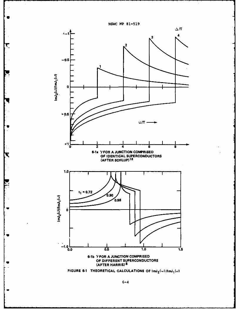
14SWC MP 81-519A/T
3 4~
.22
+0
U3
+10, 2 4 68
6-la )'FOR A JUNCTION COMPRISEDOF IDENTICAL SUPERCONDUCTORS(AFTE R SCH LUP) 18
.00.10
0.b72 O JNTINCMPIE
-16-4

NSWC MP 81-519
case for both lead and tin junctions of varying sizes measured using a
variety of techniques. These experiments are reviewed below.
6.3 Experimental Background
The major experin ental efforts to measure gamma for a tunnel junction
involve measuring the microwave response of a junction in the small signal
limit at frequencies well below the gap frequency 2A/h. The junction is
DC current biased within the zeroth order step, with an RF signal applied
such that the phase phi makes small excursions about the equilibrium
phase . In this case, the cos phi amplitude gamma contributes in a
* simple way to the RF impedance of the junction. As cosine phi can be
varied by changing the DC current bias, it is possible to systematically
vary the effect of gamma and hence separate its effect on junction
performance from that of other parameters.
Since tunnel junctions have an intrinsic shunt capacitance, it is
extremely useful to exploit the plasma resonance, whose frequency depends
on both C and cosine phi as
2W = (2 eIJcos o)AC (6-7)
The first experiment, done by Pedersen, Finnegan, and Langenberg,
involved measuring the Q of the plasma resonance at several values of9
cosine phi (and hence f P). The Q of the resonance is simply Q = 2ifpCR,
where R is given by
1 +R ( + ycos0 ) = (1 + YcOS o)/ (6-8)
The slope of a plot of f p/Q versus cosine phi for several values ofppcosine phi should yield a value for gamma from the formula
6-5
yrI
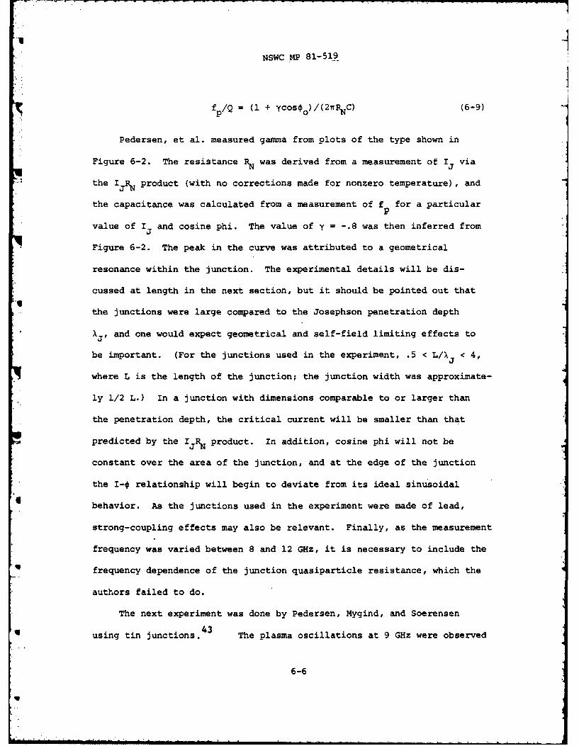
NSWC MP 81-519
f p/Q = (1 + ycOSO )/(21C) (6-9)
Pedersen, et al. measured gamma from plots of the type shown in
Figure 6-2. The resistance R N was derived from a measurement of I via
the IjR product (with no corrections made for nonzero temperature), and
the capacitance was calculated from a measurement of f for a particular
value of I and cosine phi. The value of y = -.8 was then inferred from
Figure 6-2. The peak in the curve was attributed to a geometrical
resonance within the junction. The experimental details will be dis-
cussed at length in the next section, but it should be pointed out that
the junctions were large compared to the Josephson penetration depth
Xi. and one would expect geometrical and self-field limiting effects to
be important. (For the junctions used in the experiment, .5 < L/X < 4,
where L is the length of the junction; the junction width was approximate-
ly 1/2 L.) In a junction with dimensions comparable to or larger than
the penetration depth, the critical current will be smaller than that
predicted by the IjR product. in addition, cosine phi will not be
constant over the area of the junction, and at the edge of the junction
the I-0 relationship will begin to deviate from its ideal sinusoidal
behavior. As the junctions used in the experiment were made of lead,
strong-coupling effects may also be relevant. Finally, as the measurement
frequency was varied between 8 and 12 GHz, it is necessary to include the
q frequency dependence of the junction quasiparticle resistance, which the
authors failed to do.
The next experiment was done by Pedersen, Mygind, and Soerensen
43using tin junctions. The plasma oscillations at 9 GHz were observed
6-6
V- n " n*° i . , ' - -. - - , . .L. .
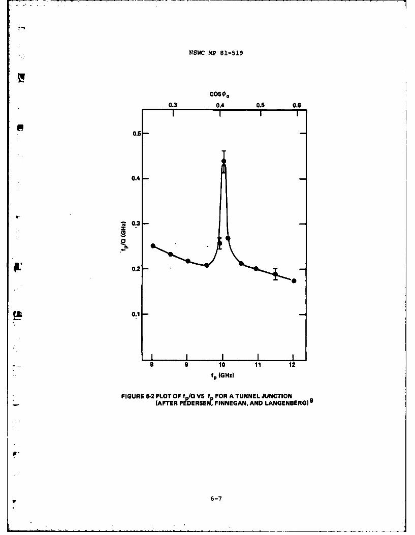
NSWC MP 81-519
COS o
0.3 0.4 0.5 0.6I I I I
0.5
OA
9-J
0.2-
0.1
8 9 10 11 12
fp (GHz)
FIGURE 6-2 PLOT OF f-/Q VS f. FOR A TUNNEL JUNCTION(AFTER PLDERS.I, FINNEGAN, AND LANGENBERG) 9
6-7

NSWC MP 81-519
over a small range of temperatures near T = T c Measurements included:
1. Exciting the junctions at 4.5 GHz and measuring their response at
9.0 GHz.
2. Observing the mixing between signals at 9 and 18 GHz.
3. Measuring the threshold conditions for half-harmonic oscillations at
an applied frequency of 18 GHz.
This last measurement was complicated by the onset of "noise rise"
due to complicated instability effects associated with the Josephson sine
phi term.4 9 However, using results from the first two measurements,
Pedersen, et al. were able to infer a temperature dependent value forV
gamma. This is shown in Figure 6-3a. The figure indicates that gamma is
positive near T - Tc, changes sign near T-o96T , and approaches -1 as T
is decreased further. At 4.2K, this is in qualitative agreement with the
work by Pedersen, Finnegan, and Langenberg for lead junctions.
9
Figure 6-3b shows the corresponding RF resistance of the junction.
The results in Figures 6-3a and 6-3b were arrived at via a complex
series of curve fits of measured junction response (e.g., mixing
efficiency, RF impedance, etc.) to equations such as 6-5, 6-6, and
6-8. Although high frequency modifications to the RSJ model were notS
considered directly, the junction parameters R and C, as well as gamma,
were treated as variables in the fitting process. This indirectly
allowed any difference between the high and low frequency values of R
and gamma to be taken into consideration. However, the many degrees
of freedom when fitting the curves allowed for excellent fits to the
observed data for more than one set of values of gamma, R, and C, as
shown in Figure 6-3c. The choice of solutions was determined by a
6-8
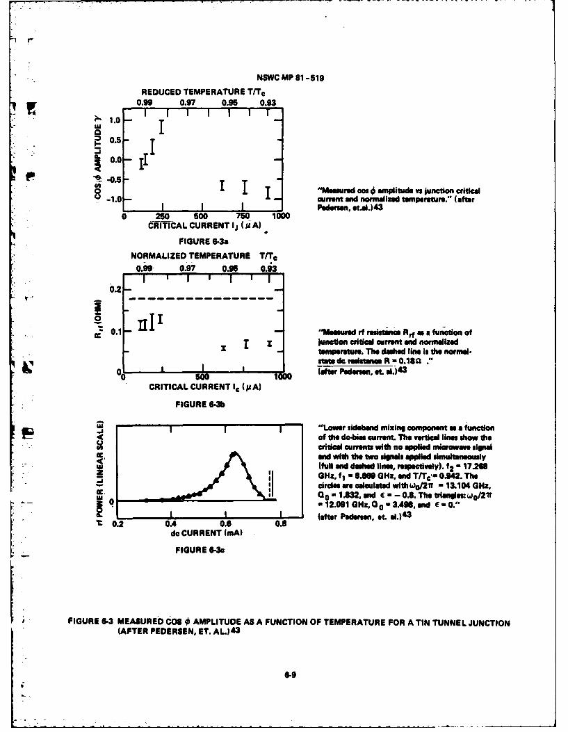
NSWC MP 81 -519
REDUCED TEMPERATURE T/T0
0.99 0.97 0.96 0.93
?1.0
0.5 j0o.0 I
8"Masuvred coo amplude vs junction critical-1.0current and normalized temperature.,* (after
Padersn, etai.)430 250 500 750 1000
CRITICAL CURRENT IJ (JA A)
FIGURE 6-.NORMALIZED TEMPERATURE T/T0
0.99 0.97 0.95 0.93
0.
0.1- "Msred rf resistance R,.1 a a funcation ofI zJunction critoal currn andw normelied
state dc resistanw R -0.18n .
(after Pedersen, et al)4 3
CRITICAL CURRENT Ic (;&A)
FIGURE 6-3b
I I "Lower sideband mixing component a a functionof the dc-bias current. The vertical lines show thecritical current with no applied microan signal
U and with the two signals applied simultaneously(full enddashedlines, rePectively). f2 17.2668GHz, f I 8.66 GHz, &d TMec 0.942. The
- s~~ircles are calculae withwg/i - 13.04 OHz.0 0i 0 - I JIM,andW E-.. The tianges: Lj/21r
12.091 OIz,Go .3.498, and E 0."c I I after Pedersen, at al.)43
.2 OA~0 0.6 0.8do CURRENT (mA)
FIGURE 6-3c
FIGURE 6-3 MEASURED COS 0 AMPLITUDE AS A FUNCTION OF TEMPERATURE FOR A TIN TUNNEL JUNCTION(AFTER PEDERSEN, ET. AL)43
6.9

NSWC MP 814519
complicated process of reconciling the calculations with the theoretical
Itemperature dependences of the plasma frequency and critical current.
(Although the Junction capacitance was a variable in the curve fitting
program, it was assumed to be independent of temperature.) The RF
resistance shown in Figure 6-3b is in disagreement with the
prediction that the IF resistance should be greater than the DC normal
state resistance and should increase with decreasing temperature (cf.
Sections 2.6 and 6.4). In addition, there seems room for skepticism
for an experimental analysis that contains so many degrees of freedom. An
independent measurement of the junction capacitance would be an obvious
first improvement to the experiment. 't should be noted that Pedersen
has a good deal of faith in the results of this particular experiment,
whereas he agrees that there are problems with the interpretation of
the results in the Pedersen, Finnegan, and Langenberg paper.
The last important experiments were done by Rudner and Claeson,
who measured the response of small lead junctions (18 micron by 18
micron) over a wide range of temperature. 4 Their primary measurement
was the microwave reflection from a single junction connected to a
* microwave stripline. The frequency (approximately 10 GHz) was fixed
while the temperature and magnetic field were varied. (The temperature
was changed between 4.2K and 7.2K.)
W As in the previous experiments, gamma, R, and C were used as
parameters in a sophisticated curve fitting routine. The results are
presented in Figure 6-4. It should be noted that Figure 6-4 supersedes
the authors' original interpretation of their microwav data.
*N. F. Pedersen, private communication
6-10
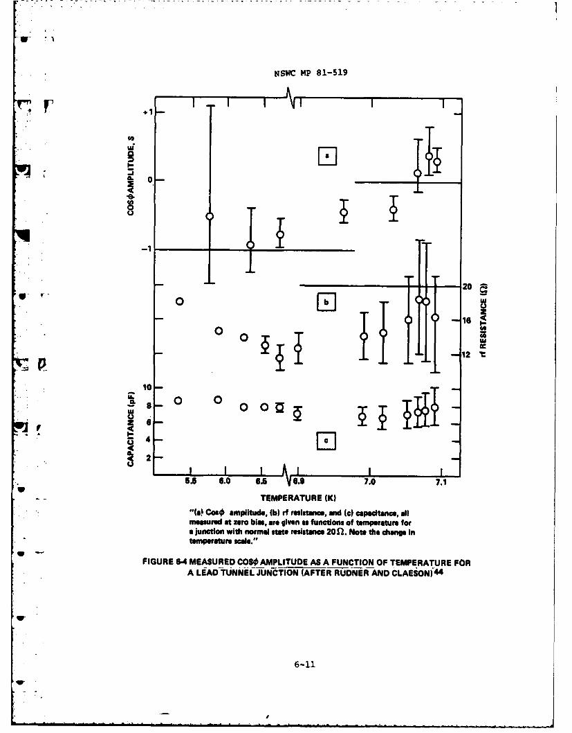
NSWC MP 81-519
-A1V
- - 20
0
II12 V
10
8-0 0
*0 0
65 6.0 6A V5 . 7.0 7.1
TEMPERATURE (K
"(01 COSO amplitude, (b) rf resistance, and (c) capacitance, allmeasured at zero bin, are given as functions of temperature fora junction with normal state resistance 20fl. Note the change intemperature scale."
FIGURE 6-4 MEASURED COSO MPLITUDE AS A FUNCTION OF TEMPERATURE FORA LIEAD TUNNiEL JNTION (AFTER RUDNER AND CLAEiON) 44
6-11

• *1
NSWC MP 81-519
As in the Pedersen, Mygind, and Soerensen experiment, there seems good
reason to be skeptical of an experimental technique that relies on the
accurate fit of so many variables to a theory that is at best an
approximation. For one thing, the curve fit depends on an extremely
accurate assessment of the VSWR and insertion loss of the microwave
circuitry external to the cryostat. In addition, there might be un-
recognized problems associated with the use of an external magnetic field
as the independent parameter (e.g., problems with screening and trapped
flux).
The plot of capacitance versus temperature in Figure 6-4 seems
reasonable, as C is expected to be independent of T. However, one would
expect the RF resistance to increase dramatically as T is reduced (cf.
Figure 6-5, equation 6-12). This is not the case, and the peculiar
fluctuation of RN with T in Figure 6-4 suggests that there are some
problems with the experiment.
However, the results of Rudner and Claeson are qualitatively con-
sistent with those of Pedersen, Mygind, and Soerensen and Pedersen,
Finnegan, and Langenberg. Given that the experiments were done by
measuring different quantities on different sized junctions--made of both
0 lead and tin, there seems little doubt that there is a genuine discrepancy
between the actual and theoretical values of the cosine phi amplitude.
6.4 High Frequency Corrections to the Plasma Resonance Experiment
W At this stage it is worth investigating the Pedersen, Finnegan,
and Langenberg experiment in detail. Unlike the other two experiments,
the microwave frequencies at which the junction respon.se was measured
W varied over a wide range. However, the frequency dependences of the
6-12
VP

NSW MP 81-519
41J
w.T 10 0.9
6.5(b)0.1-
0.05-
y *0.0047 +0.4579x
L. 0.I
FIGURE 645 IffJ (W) AS A FUNCTION OF FREQUENCY ANDTEMPERATURE (AFTER YOUNG)52
6-13

NSWC MP 81-519
quasiparticle resistance and the cosine phi term were not taken into
account. This can be done using the Werthamer theory, and is shown
below. As the Pedersen experiment was done using lead tunnel junctions
at liquid helium temperatures, the following discussion has been
specifically directed to lead junctions at 4.2K.
The Pedersen experiment was done at frequencies between 8 and 12
GHz. Normalized to the measured gap frequency 2A/h of 616 GHz for lead,
we have a reduced frequency that varies between .0260 and .0390 on the
graph of Im J versus frequency in Figure 6-5 (after M. Young52). The
transition temperature of lead is given by Rickayzen as 7.2K, whichI 48yields a reduced temperature of .58. The line for T/T in Figure 6-5c
for T = .6 was digitized for the interval .026 < f < .039 to yield y -
.0047 + .4579X. Scaled to the gap parameter and critical current, this
gives an expression for Im J1(f) of:
Im Jllf- 2 I (0){.0047 + .4579hf/A} (6-10)
1 wJ
(If the graph had slope -1 and y intercept = 0, as in the RSJ limit,
then we would have Im J (f) - (2/w)lIj(0)(hf/4). At f - 26/h, Tm Jl(f) -
(4/w)I (0), which is consistent with an IjR product of ! .)
f For the plasma resonance experiment,
f /Q - l/(2wRC) , whz /R - (1/Rf) (1 + ycos* 0 1 (6-11)' p
* where Rf is the quasiparticle resistance at a particular frequency.
It is important to remember that the ratio gamma, as well as co,
depends on frequency. In the argument that follows, gamma will be treated
* as a constant, and we will be concerned with the frequency dependence
6-14
- - - - - -- - - -mm m lm~m mu . .,

NSWC MP 81-519
of ao. The frequency dependence of gamma will then be added in a
qualitative manner. Werthamer and Harris give a derivation of the high
frequency quasiparticle resistance which leads to the following" . 5,15
expression (cf. section 2.2):
1 e Im J (f ) (6-12)RN hf 1(f
So,
p 1 e 2 hfx - x -I.j(0) (.0047 + .4579 (1 + Ycos*O ) (6-12)21rC h r
where I (0) is related to RN by I(0) = TA/(2eRN).
Thus:
1 E.c 47A(O) + .457 (l + ycos o ) (6-15)
NOTE THAT FOR y = 0, f /Q WILL DECREASE WITH FREQUENCY.p
Cosine phi can be written as
COs = .hCfp (6-16)eI (T)
Note that I is the measured value of I at a particular temperature.
This will be different from Ij(0). (As Young's calculations were scaled
with respect to A(0), RN, and Ij(0), it is correct to use 1T(0)/( 2 eR) =
1 (0) for calculating Im Jl(f) at T not equal to zero.) For the time
being, let I (T = .6Tc) = I (0). Any inaccuracy this causes can be
subsequently corrected by modifying gamma slightly, as YcosO =
y7rhCf p2/e I
We now have
6-15
NSWC MP 81-519
fI
1 .0047A(o) + 4579} (1 + l,2rhc2 (6-17)27C hfP e P
Pedersen, et al. give RN - .46 ohm, and C = 1.5nFd (8). A(0)/h is
308 GHz. Rewriting whC/eI as (2NC)/[A(0)/h] we have
f .2307 C2 (6-18)-F- + .46] [1 + y x 4.48 x 10- f 2 IP pp
where f pis in Gigahertz. This is plotted against Pedersen's results
for several values of gamma in Figure 6-6. (Pedersen's graph is not
very accurate, as evidenced by the disagreement between his line for
1/121%C) and a replotted l/(2nRNC) - .2307. Presumably, the inaccuracy
is a result of artistic license when the graph was prepared for
publication-)
Figure 6-6 is based on the assumption that gamma is constant. With
reference to Figure 6-1, it can be seen that gamma decreases with
increasing frequency. In terms of f /Q versus fp, this means that onep /
should draw a "load line" on Figure 6-6 reflecting this decrease. This
will have the effect of shifting the line for f p/Q versus fp downwards with
increasing f for positive values of gamma, and upwards with increasingp
f for negative values of gamma.
Figures 6-7 and 6-8 show f /Q versus f repeated for T - .6Tc andPp
for T = .7T (also based on Young's calculations). Note that the linec
for gamma = -1 is by no means the obvious choice for explaining theV
data of Pedersen, et al. It is also interesting that f p/Q is so sensitive
to the reduced temperature. (The frequency dependence of gamma has not
been included in Figure 6-7 or 6-8.)
6-16
U t

NSWC MP 81-519
Cos4G.
0.3 0.4 0.5 0.6
I I I I
0.5
0.4
PEDERSEN,et. al. LINEFOR
0.3 21rRNC
- -- - - -- RNC 01.=7
y -+0.5
0.1-
Y- -10
"* 0 I I I I8 9 10 11 12
fp (GHZ)
FIGURE 64 PLOT OF fo/Q VS fo FOR A TUNNEL JUNCTION, INCLUDINGCALCULATIONS OFf,/O - 3(1+Ycoa) (AFTER PEDERSEN,FINNEGAN, AND LAIGENBERG) 9
6-17P".,.I

NSWC MP 81-519
0.5
T/ -_0.6
0.4
f,,/, -10.2307 [1.4/fp +10.461 [1 +Y x 4.48 x 10³f (f i .GHz)
0.3 1
-, : /21YRNC -
- I+1
0.2
7" 0
0.1 '7 - -0.5
7 -1
l . . . I I , I9 10 11 12
FIGURE 6-7 fp/Q VS FOR TtTr-. 0.6
6-18

NSWC MP 81-519
0.5 IF fp IS IN GHz, THEN
f,,/a .i.23o7 [L*-r1, 0.721 [1 +Y (4.48,1 x 1-3)]fp 0 -023- 5
0.4 T/Tc 0.7
..- ' -+1
- 0.3
0 ' -0.5
- -/2"rr-R-NC 0.2307
. 0.2 7-'0
0.2 - - - 0
p----1
II I ia 9 10 11 12
fl (GHz)
FIGURE 64 fp/0 VS fp FOR T/T0 - 0.7
6-19
rq

U
NSWC MP 81-519
It is difficult to draw any definite conclusions from the above
analysis without knowing more details for the experiment. However, the
foregoing discussion suggests that the RSJ model is inadequate for
analysis of the cosine phi problem. Several other points concerning the
data merit discussion.
First, Pedersen, et al. computed RN from the IjEN product using the
value for I measured at T = 4.2K. They did not take into account that
( 'A (T) [A(T)]I s(T ) _ 2 e x ta L -- -- (6-19)
JeR 2kT(
If we assume that A(4.2K) = .9A(0), and 2A(0)/kT = 4.1 (after
Rickayzen 4 8 ), then
I j(4.2k) = .82 I j(0) (6-20)
This change in I would cause a corresponding change in the calculated
value of RN such that RN - .38 ohm, instead of .46 ohm. This would have
the effect of shifting l/(2wRNC) upwards in Figure 6-6.
On the other hand, lead is a strong-coupling superconductor, and a
lead junction is expected to have a critical current that is approximately
4015% lower than that predicted by BCS (see Ginsberg and Harris j. This
Wwould mean using a value of I(0) that is 15% lower than the BCS value
when computing the IjR product. In other words, the temperature
correction of I is offset by the strong-coupling correction, and the
value of .46 ohm for RN is probably reasonable. (According to Pedersen,
neither of these corrections was taken into account.*)
Second, the normal-state resistance was not measured independently
Vduring the course of the experiment. Nor were the DC I-V characteristics
*N. F. Pedersen, private communication
6-20
W

NSWC MP 81-519
recorded. The quality of the junctions was ascertained by comparing
the height of the zero voltage supercurrent with the height of the
current "knee" at V = 2A/e. (This agreed with theory, including the
strong-coupling correction for lead.)
Third, there is an inconsistency between two sets of measurements
reported in the Pedersen paper. The authors present a plot of the inverse
Q of the plasma resonance versus the critical current at fixed frequency.
The data was obtained from several junctions having different values of
I. V The RSJ theory predicts that the inverse Q should vary with critical
current as
1 (1 + Ycos4o)/(21TfRfC) (6-21)
where Rf is the resistance of the junction at the plasma frequency and is
given by
* Rf = hf/[eImJl(f)] evaluated at f = f (6-22)1 p
' Substituting
coso - fICW 2 /[2eI (T)] and RN = 2ej(O)
p e J(0
we have
1*c 2
1 = [2eI (O)/(27T2f CA(0))] il + -I2)Q p R 2e1 (T)
Note that as I j approaches zero, 1/Q approaches
1= RNY§- [2fif 1 (0) 1/[DTA(0) I(T)I (6-24)
p J
6-21
wI

U4
NSWC MP 81-519
The published graph (cf. Figure 6-9) suggests that at Ij - 0, l/Q
is approximately .001. If we assume that Ij (T) - I j (0) and Rf=RN, then
1/Q should approach
Q 7TA(0) (6-25)
For lead, A(0)/h = 308 GHz. In the experiment, f M 9 GHz. If 1/Q =p
.001 when I is zero, then Figure 6-9 suggests that gamma - .11.J
On the other hand, if gamma is -1, then 1/Q for Ij M 0 should be
approximately -.01. Figure 6-9 suggests that this is clearly not the
case.
Finally, the lead tunnel junctions used in the experiment were quite
large with respect to the Josephson penetration depth:
.5A J < L< 4A J
This suggests that geometrical and self-field effects could have a major
effect on "the experiment (cf. section 6.3). This is supported by the
observation of the resonant peak observed in f p/Q versus f p measurements.
6.5 Theoretical Work
In the previous sections we have discussed the various cosine phi
measurements. They have obvious shortcomings, but the conclusion that
gamma is negative when theory predicts it to be positive is difficult
to refute. In an effort to provide a theoretical basis for the
experimental observations Kulik, Schrieffer, Likharev, et al. have
q reanalyzed the Werthamer theory in terms of the derivations of the
41response functions J (M) and J 2 () . As Im J2 () is related to Re J 2 (w)
via the Kramers-Kronig relations, Kulik, et al. surmise that a broadening
of the Riedel peak in Re J 2 (b) can lead to regions where Im J 2 (W), and
6-22
q

NSWC MP 81-519
H
T m4 2K/
9- . I 1
a .*71f /
-[.05 /
* .0"p *I 'H~ 4t.0
.02 H - 13
T - 4.2K
1 -S GHz
0 4 8 12 16 20 24
Ij (mR)
!FIGURE 6-9. 1/0 VS I FOR A TUNNEL JUNCTION (AFTERPEDERSEN, ET AL, REF 9)
6-23
NSWC MP 81-519
consequently gamma, are negative below the gap frequency. Of the various
causes of smearing of the Riedel peak, they conclude that inhomogeneity
of the materials comprising the junction electrodes leads to the cosine
phi behavior most consistent with experimental results.
Pedersen and Rudner-do not believe that the Kulik explanation fits
the cosine phi behavior they have observed in their different experi-
ments.* Kulik, et al. conclude that smearing of the Riedel peak
will cause gamma to be positive at high temperatures, but negative as T
approaches zero. However, the temperature at which gamma switches sign
is near T = T in the experiments. The Kulik theory apparently cannotW c
explain the occurrence of the sign change at a temperature so close to Tc
Another explanation as to why gamma might be negative is the popular
relaxation effect which arises from time-dependent Ginzburg-Landau theory
in connection with microbridges.45,46 This theory seems to have no basis
for a tunnel junction (cf. Chapter 5).
6.6 Suggestions for Future Work
The final conclusion of this chapter is that there is still a major
discrepancy between theory and experiment concerning the amplitude of the
cosine phi term. Of the three experiments, the original Pedersen,
"* Finnegan, and Langeberg experiment seems to be the most amenable to
theoretical interpretation, as opposed to complex numerical analysis.
However, the original experiment was done using large junctions made of a
Sw strong-coupling superconductor. Unfortunately, many of the quantities
necessary for an accurate interpretation of the data were not measured
(e.g., the DC I-V characteristics measured under current and voltage
* gbias conditions), and the high frequency corrections to the RSJ model
'Private communications with N. F. Pedersen and S. Rudner
6-24
F-

NSWC MP 81-519
were not taken into account. Furtheimxore, to account properly for
geometric and large junction effects could be extremely difficult.
it seems likely that if the Pedersen, Finnegan, and Langenberg
experiment was repeated more carefully, over a wider range of frequencies,
and with smaller junctions, it would yield much useful information. The
use of lead, tin, and lead/tin combination junctions in the same geometry
would allow one to identify any anomalous effects that might occur due
to geometry or peculiarities of the material. Finally, the direct
measurement of RN and Im J 1(V) from the I-V characteristics, as well as
an independent assessment of the junction capacitance, should remove some
of the doubts about existing experimental results. In conclusion, there
seems to be a good case for repeating the original plasma resonance
* . experiment.
6-25/6-26
I2NSWC MP 81-519
CHAPTER 7
1FILTER DESIGN
7.1 Introduction
The numerical technique that was used to design the filters for
T = 0 failed consistently when attempts were made to design filters that
model J (W) and J (w) for finite temperature. The numerical calculations1 2
yielded Pade approximates for J and J2 that were neither accurate nor
- causal. It is not difficult to show that the expressions for J and J1
are causal, so one can be confident that an accurate approximation to J
* and J2 will also be causal, or can be made to be causal with only slight
modification. However, there was the distressing possibility that J and
J for finite temperature could not be modelled accurately without an
inordinate number of poles. This turned out not to be the case, and the
synthesis problem was finally solved by using the existing numerical
F, design technique with a new twist. The resulting Pade approximates for
L J1 and J2 at finite temperature are quite good, and have since been trans-
formed into electronic filters. The improved version of the electronic
analogue can model the Josephson effects at T = 0, T = .72T andc
ST = .9T.c
In this chapter, we discuss the design and evaluation of the new
* filters. However, before describing the actual methods involved, there
is a brief section on some of the basic properties of the functions
k J () and J () "
F It should be remembered that although the design of these filters
is engineering, and not physics, this subject is crucial to the
development of the analogue. The synthesis techniques described herein
are, to the best of the author's knowledge, completely new and are not
I

NSWC MP 81-519
based on standard electrical engineering techniques. The idea for this
method was not suggested to the author by anyone, although in retrospect
it seems like an obvious route to pursue.
7.2 Discussion of J and J2
The Werthamer paper presents a derivation of the functions J1 and
J2 in terms of the BCS theory and the assumptions about tunnelling
presented in Chapters 2 and 5. However, Werthamer and subsequent
authors say little about two properties of these functions that are5,8,18,19
central to the design of the electronic analogue. First, it
has tacitly been assumed that as functions of time, j 1 (t) and j 2 (t) are
causal. Second, it has been assumed that the functions are real.
If the functions j 1 (t) and j 2 (t) were not causal, it would be impos-
sible to build filters which could be connected in such a way as to
model the current through the junction. However, as the values for jl(t)
and j2 (t) for t < 0 have no effect on the current through a tunnel junc-
tion (cf. eq. 7-1), these functions can always be modified so as to be
causal. Fortunately, the expressions for Jl( ) and J () as derived by1 2
Werthamer and others already satisfy the Kramers-Kronig relations, and
need no modification.
I(t) - {e Jl 2 (t-t')dt' +.e 2 e j 2 (t-t')dt'} (7-1)
If the functions were causal, but not real, it would still be
possible to build the analogue. Substitution of a complex function for
i(t) or J2 (t) would complicate matters, but one could still model
w Equation 7-1 electronically. This would require construction of
7-2
Vq

NSWC MP 81-519
separate filters for the real and imaginary parts of each function, which
would then be connected to the proper combination of sin phi and cos phi
signals.
As it turns out, j1 (t) and j2 (t) can be regarded as being real.
In the case of tunnel junction comprised of identical superconductors,
this can be demonstrated for j2 (t) using the condition that the junction
must be insensitive to the polarity of the bias voltage, and the current
- must, therefore, be an odd function of voltage. In the voltage bias
limit, we have
f - 2eV/h (7-2a)
and
I(V) - ImJI1 (V) + ReJ2 (V)sinO + ImJ2 (v) coso (7-2b)
By inspection, we see that Re J 2(V) must be an even function of
voltage, as phi changes sign when V does, and sino is, therefore, odd.
Likewise, Im J 2(V) must be odd, because cos is even. The inverse
Fourier transform of a function whose imaginary part is odd and real
part is even is a real function of time.
Although Re J (V) does not show up explicitly in equation 7-2b, one is
tempted to believe that a similar macroscopic argument also holds for
J (t).•
In the microscopic limit, the derivation of jI(t) and j2 (t)
involves the sum over states of both hole and electron like excitations.
Completely unrelated to the argument concerning bias polarity, one can
show that the existence of symmetry between these hole and electron
states will result in j1 (t) and j2 (t) being real in the general case,
regardless of whether the junction is comprised of identical super-
7-3
'U
. . . nu m j
j lm n mu -mmunm

NSWC MP 81-519
conductors. * This hole-electron symmetry allows a one-for-one pairing
between hole states at a particular energy below the Fermi energy, and
electron states at the corresponding energy above the Fermi energy.
This correspondence results in the sum over states, and hence, j 1 (tM and
j2 (t), being real.
Strictly speaking, the hole-electron symmetry is not exact. How-
ever, because the Fermi energy of a superconductor is so large compared
to the range of energies that contributes to the summation described
above, it is a very good approximation (e. g. , good to one part in ten
thousand), and it is sufficient to say that hole-electron symmetry, as
well as the parity requirements placed on the bias voltage, make it
valid to treat j 1(t) and j2(tW as real functions of time.
7.3 The Design Problem
The previous failure of the Pade approximate technique was a
result of two things. First, the choice of data points was not
always consistent with the frequency resolution attainable by a Pade
approximate having a given number of poles. Second, accuracy limitations
of the data used for the calculations were not taken into account.
The first problem is related to the fact that there are no
analytic pole/zero expansions for J 1andJ2#enfoT-0.Ial
likelihood, this means that it is ir'possible to model the functions
exactly with a Pade approximate having a finite number of poles. The
limitation that this places on the choice of data points can be under-
stoodJ from the following properties of Pade approximates.
*J. R. Waldram, Personal communication
7-4

NSWC MP 81-519
p1. The number of poles in the Pade approximate is equal to the number
of frequencies at which the approximate is set equal to the original function
(e.g., the number of data points used in the calculation).
2. If the Pade approximate has less poles that the function being modelled,
the approximate need not be causal.
3. If one uses a sufficient number of data points, it is possible for the
Pade approximate to have more poles that the function being modelled. For
example, if data at ten frequencies are used to calculate an approximation
to a function having six poles, the Pade will contain four pairs of poles and
zeros having the same location in the complex frequency plane. These extra poles
and zeros need not lie in the left half of the complex frequency plane
(i.e., the, causal half-plane). The Pade approximate will remain causal, as the
excess poles are cancelled by the zeros at the same locations, and have no
effect on the Pade approximate.
If we are interested in modelling J 1 or 12with a Pade approximate
having a finite number of poles, the data points must be chos".n so as
to represent a function having no more than this number of poles.
Roughly speaking, this suggests that to model accurately a function
over a bandwidth f using n data points, no details requiring frequency
resolution better than f/n should be included in the calculation. In
thecae o J1 nd J 2 P this means that there is some limitation on the
accuracy with which the gap singularity can be modelled simultaneously
with the broad structure away from the gap for a given number of data
points. If one tries to model too much of the curve with too few data
points, the resulting Pade approximate will be neither accurate nor
7-5

NSWC MP 81-519
causal, even though it will fit the original function at all of the data
points. (Nevertheless, practical experience indicates that more data
points should be taken from near the Riedel peak than from regions con-
taining no fine structure.)
The second problem is more subtle. Assuming that the Pade approxi-
mate has more than enough poles to model the original function with
the desired resolution, there will be extra pole/zero pairs lying in
both the left and right half-planes. These will be in addition to the
poles and zeros, which are not paired, which represent the original
functions. If the real and imaginary parts of the input data are subject
to small, uncorrelated error, the poles and zeros will move from their
original positions. In the case of the unpaired poles and zeros, the
shift in position will equate to random noise in the Pade approximate.
However, all of the unpaired poles should remain in the left half-plane.
At the same time, the paired poles and zeros will move slightly, such
that they are still approximately paired, but no longer identical. This
ILWJ will also appear as random noise. However, as the right half-plane
poles are no longer matched by zeros, the Pade approximate will
become noncausal. From a slightly different point of view, the
* uncancelled poles in the right half-plane result from the essentially
non causal error to the original data.
An increase in the number of data points used in the calculation
* will result in two benefits. First, the amount of detail that can be
modelled will increase. Second, the effect of inaccurate data will
decrease. Using simple statistical arguments, one would expect the
V accuracy of the overall fit to improve as the square root of the number
of data points.
7-6
NSWC MP 81-519
7The new filter design technique is based on using 15
judiciously chosen data points to calculate a Pade approximate, and
then removing any noncausal poles and their closest zeros. In addi-
tion, there will usually be a comparable number of causal poles which,
along with their closest zeros, can be removed with little effect on
the Pade approximate. The resulting seven or eight pole function is
then used as the basis for an electronic filter.
An example of such a calculation is shown on the next few pages.
Data for J 2(w) at 15 frequencies is obtained by digitizing
published graphs. 8,5The data, plotted in Figure 7-1 with the graph
from which it was obtained, is used to calculate a 15 pole Pade approxi-
mate (cf. Table 7-1). This is factored to yield its poles and zeros,
which are plotted in Figure 7-2. After deletion of the paired poles
and zeros (circled in the figure), the Pade is reconstructed (cf.
Table 7-2). Figure 7-3 compares a plot of the original 15 pole Padi;
approximate, which is noncausal, with the new seven pole approximate,
which is causal.
Figure 7-4 shows a comparison of the original function with the
measured response of an electronic filter designed using the results
in Table 7-2. (The gap frequency of the filter is 1 kHz; the plot
was obtained using a computer controlled frequency response analyzer,
and the difference between the computed and measured filter response
is negligible.) The overall fit of the filter response to the original
function could be improved by using additional data points near the
gap singularity. However, this would have resulted in a more complex
filter, and it was felt that the design of filters containing more than
7-7
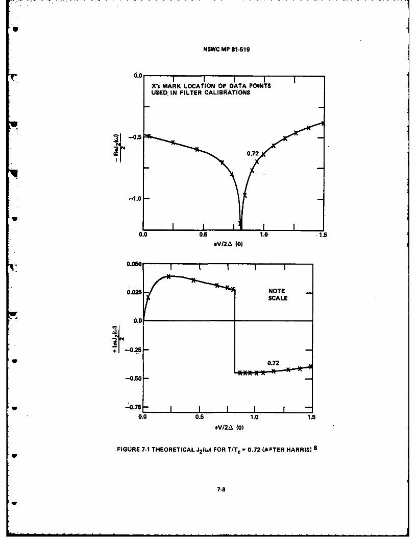
NSWC MP 81 -519
0.0 IX's MARK LOCATION OFDATA POINTSUSED IN FILTER CALIBRATIONS
7;
CC 0.72
000.5 1.0 .1.5oV/2A (0)
0.025-NOTESCALE
0.72
000.5 1.0 1.5
9V/2,1 (0)
FIGURE 7-1 THEORETICAL J2(wo) FOR T/Tc 0.72 (AFTER HARRIS) 8
w
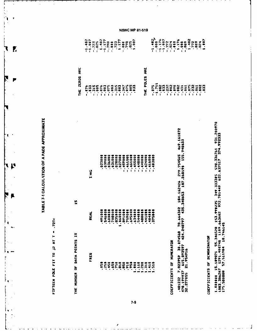
Y
NSWC MP 81-519
° 4c . . . .* o4 .N w -. °.
W 4
co0 hw 0 .
isw :1WS aw ace ~ p .w "4 ISM -a~e~A:eMI ~V I-till l 'I lot ll 4!
Z °
in
I- -
II -u 0o
a I
0~1 In In -
: .4
0 W %vv
4! ..C !'OC -
o 11.4111IS i4w
I4 PL a0f
4n Co .aj r0
c we
.1 P 1 a M- .0to ow 0I..1 Sin,
I- W In 'a a w N .4 4 w in 4
4l IPI 40.4
to~~t N444.
Cc i .41 I- ew 1" .4 4 U4 v0x -. Z CDI"
4C = U Mco W CDI.- Z W~0 U;o oc I). CoMi. a NJ
La Llfl41l4Uin4.. 0 .0 CDtW ~ ~ 0................................ .. . . .. C *Cw .4 IS
J444... P- I-. t- Is cC1 m in 0 z Ncc1 1Y ISI "a

I-INSWC MP 81.519
0 0%
U o.- o-
0 0 0I-
UL
Naz
LU
NN
IWI
7-10

LLL NSWC MP 81-519
20 me
v .
Lu -*...I-0'd~' eeleeee
I.-.LA.a
zIn n * q.@4 10 *pNulaue0
.4 1Fcm P t
0 Owcc a
Lu CCq
'A
00O 0
I • y) 4OO.
I.Lu
ILU
II
LulE. 00 :
.60
0 a7e1
I "e- Cee7-11

NSWC MP 81 -519
2 SOLID F IFTEEN POLE, NONCRUJSRL[ ORSHED -SEVEN POLE, CRUSRL
1.3 ae3
-2
FIGURE 7-3 ATTEMPT TO FIT J2AT TIT, 0.72
7-12

NSWC MP 81 -519
0.0 I
$ 0.72
0.0 0.5 1.0 1.5
SLWI2Ao
0.025 NOTESCALE
0.0
-00.72
0.0 0.5 1.0 1.5
1ftI/2AO
FIGURE 7-4 MEASURED RESPONSE OF THE ELECTRONICFILTERS FOR J2 (W) AT T - 0.72 Tc (THEORETI-CAL CURVES AFTER HARRIS)
7.13

NSWC MP 81-519
seven or eight poles would not be practical. Figures 7-5 and 7-6
show measured responses of the filters that model tunnelling at
T - .72T cand T - .9T * A photograph of the most recent version
-. of the analogue, which contains these filters, is shown as the
frontispiece of this dissertation. Results obtained using the analogue
with these filters are presented in Chapter 9.
7-14

NSWC MP 81-519
LO
I--
44L
0 q 00
0 L
0 :3
4q 4to
toF
lr* NV4 NU
(O)v (M~)rINU 3 (01 vz/(Cn~)zg. WJI N
0U.
C!CU-.
00
aa z4 Mo
MA
I- I I I MA
j OP)/Z/((II Ir wl Nil-N.1*E M *o g
7-15
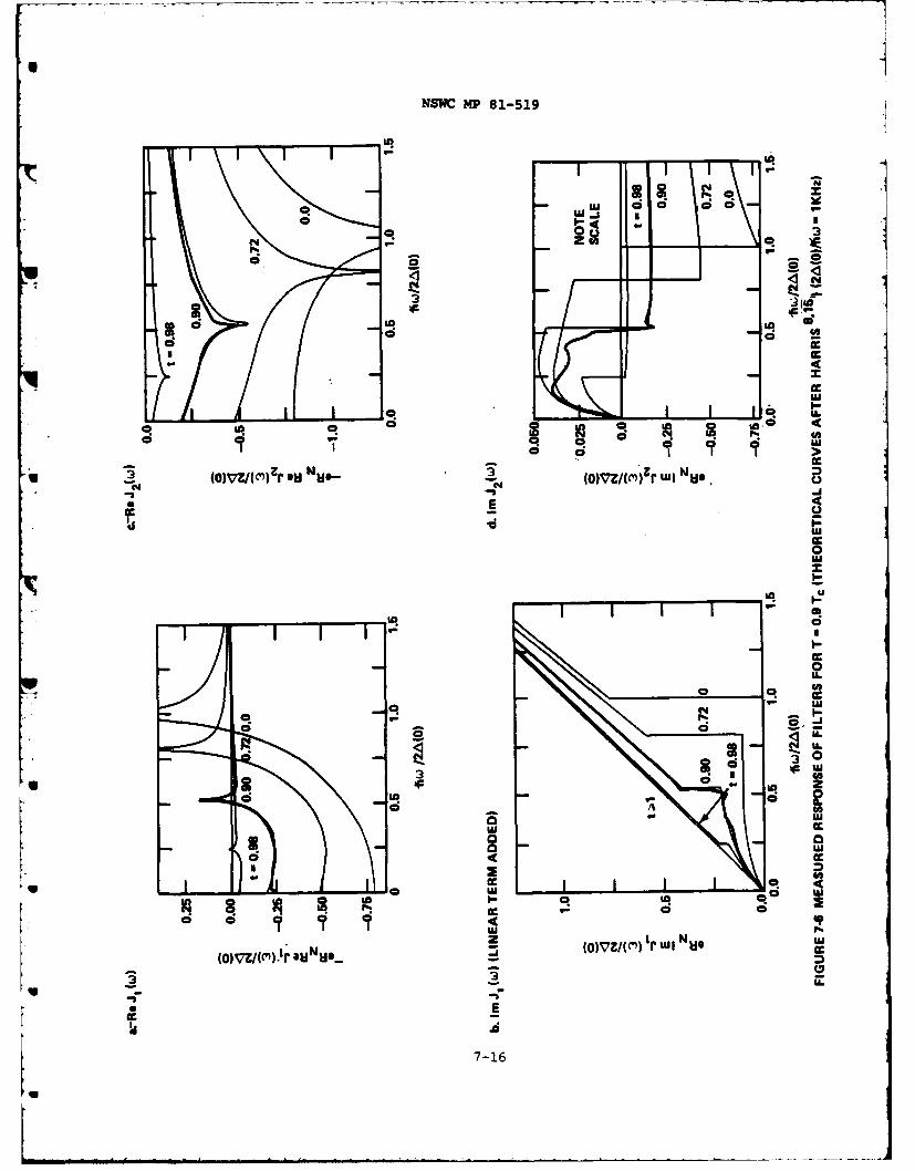
NSWC MP 81-519 *
32~k@0
I-.
0 >~cc
N3 - .Mcn 3 e ml-( M I M w 9
Sj30
<
I 0 0U -
.
01, 4c u
U
LU.
0*to?, cc
au3 u
N~~~~S 'FVA)IrW sc
C7 1

NSWC MP 81-519
CHAPTER 8
ACCURACY OF THE ANALOGUE
8.1 Introduction
The results presented in previous chapters indicate that the
electronic analogue is capable of providing a good qualitative fit to the
Werthamer theory. However, efforts to obtain good quantitative data were
complicated by several problems, such as noise within the VCO, the
unwanted cos phi term introduced by the phase shift of the low pass
filters, errors resulting from difficulties in adjusting the DC offsets
of the multiplier chips, and an assortment of measurement problems. After
additional study, these problems were overcome, and it became possible to
compare the performance of the analogue with other calculations and data
in a quantitative, as opposed to a qualitative, manner.
In this and the next chapter, we describe how these problems were
overcome, and discuss the results that have since been obtained. The
discussion begins in this chapter with a summary of the various improve-
P ments to the circuit design, and an assessment of the accuracy of the
analogue. This is followed in Chapter 9 with a comparison of results
obtained using the analogue with an assortment of theoretical and
experimental results.
8.2 Sources of Error in the Analogue
The accuracy of both the RSJ and Werthamer analogues is affected
by several factors, which are listed briefly below:
1. Component Accuracy
2. Multiplier Accuracy
3. VCO Harmonic Distortion
8-1
0 .,

Ui
NSWC MP 81-519
4. LO Harmonic Distortion
5. VCO Gain Linearity
6. Transconductance linearity of the voltage controlled current source
(vccs)
7. Output impedance of the VCCS
8. Temperature drift of the LO and VCO center frequencies
9. Op Amp accuracy
10. Phase shift introduced by the low pass filter (LPF)
11. High-frequency rejection of the LPF
12. Noise pickup
13. VCO phase jitter
14. Accuracy of the phase shift between the sin phi and cos phi signals
15. Accuracy of the J and J2 filters
Many of the above quantities can immediately be characterized in
terms of percent accuracy. For example, the resistors and capacitors used
in the analogue are rated at 2%. The multipliers have an accuracy of .25%
over the bandwidth used in the circuit. The harmonic distortion of both
the VCO and LO is less than 1%, and the VCO gain is linear to approximately
1%. The transconductance of the voltage controlled current source is also
constant to within 1% over the operating range of the analogue.
Other items from the above list must be described in terms of the
operating parameters of the analogue. For example, t.e output impedance
of the VCCS appears in parallel with the shunt resistance of the analogue,
and can be considered as an error to the value of the shunt resistance.
The VCCS output impedance is easily adjusted to be greater than 200 kilohm,U
which has less than a one percent effect on the apparent value of the
8-2
L

NSWC MP 81-519
U Josephson shunt resistance, which is typically 1500 ohms or less. (However,
at voltages less than the gap voltage, the resistance is considerably
higher than R., and the output resistance of the VCCS could be important.J
This turns out not to be the case, and in any event, one can always measure
the effective resistance directly from an I-V curve.)
Another important factor which can be a source of error concerns the
temperature stability of the VCO and LO. This determines whether the
operating point of the analogue will drift with time. For example, a
change in either the VCO or LO center frequencies will have the same effect
* on the junction current as a change in input voltage. The VCO and LO used
in the analogue are commercial units and have extremely low temperature
drift. Over the course of several minutes, there is no observable change
in the bias point; even over a period of several hours, drift is almost
negligible.
The remaining sources of error are more complicated, and will be
IL discussed individually in the next sections.
8.3 Accuracy of the Op Amps and Multipliers
Inaccuracies due to op amps generally result from two things. First,
most circuits that use op amps are designed on the assumption that the
-gain of the op amp is infinite. This is not a good assumption at high
frequencies, but is quite reasonable at the frequencies at which the
analogue operates. The second problem is the effect of the phase shift
introduced by the compensation capacitor inside the op amp. This
capacitor, which prevents parasitic oscillations, causes the op amp to
behave as a single-pole low pass filter, and introduces a slight cosine
phi term having negative am~plitude. This term can be made negligible by
8-3

NSWC MP 81-519
yr using an op amp having a very high cutoff frequency. However, the higher
the cutoff frequency of the op amp, the more susceptible it is to noise
pickup and instability.
Fortunately, the phase shift due to the accumulation of op amps, each
contributing a slight phase shift, has a negligible effect on most
measurements done using the analogue. For one thing, many of the circuits
used in the analogue have a considerable amount of capacitative feedback
anyway, as in the case of a biquadratic filter. Second, many of the op amps
in the analogue are nested in multiple feedback loops, which reduces the
influence of the compensation capacitors very dramatically.
The influence of op amp phase shift was noticed in the evaluation
of an improved low pass filter circuit, and in some of the plasma
resonance experiments. These effects could have been reduced almost
totally by using op amps having a cutoff frequency higher than that of
the ubiquitous 741 type ampliier. However, the op amps are not the major
source of cos phi error (the LPF is), and in the interests of minimizing
noise pickup and instability, it was decided not to change to a different
op amp. (Quantitative details about these effects are included in the
discussion of the lowl pass filter design in Appendix D, and in the
presentation of plasma resonance data in the next chapter.)
Related to the discussion of op amp accuracy is the question of
multiplier accuracy. As mentioned above, the multipliers used in the most
recent versions of the high frequency and RSJ analogues are specified as
being accurate to .25%. This is a considerable improvement over the
multipliers used in the previous version of the analogue, which were quoted
at 2%. However, the more important practical consideration is that the new
8-4

NSWC MP 81-519
multipliers are internally trimmed, and do not require external potentio-
meters. This results in an elimination of 18 adjustments which, in the
earlier analogue, were difficult and time consuming. The new multipliers
p (Analog Devices Model AD534) were considerably more expensive ($50 as
opposed to $14 each), but were well worth it, and their accuracy seems to
be more than adequate. Hopefully. the results presented later will present
a convincing argument for this.
8.4 VCO Considerations
The next four items from the list of possible sources of error are
interrelated in a complex manner. The LPF, which determines how well the
unwanted VCO center frequency is removed from the sine and cos phi signals,
and what the unwanted cosine phi amplitude will be, is designed in
accordance with the choice of the center frequency of the VCO. In turn,
the choice of VCO center frequency is related to the problems of noise
pickup and VCO phase jitter. In this section, we consider the operating
'A parameters of the VCO.
Generally speaking, there was no difficulty in arranging the signal
levels in the VCO circuitry so that the signal to noise ratio was
acceptable. However, noise at the input to the VCO is of special interest,
as it causes errors in the phase phi. With the VCO as originally set up,
it was difficult to keep the noise pickup at the input at a sufficiently
low level. The problem was solved b deliberately reducing the VCO gain
constant, while increasing the level of the input signal.
Related to the noise pickup is the problem of phase jitter within the
VCO. This results from the internal operation of the VCO, which in tne
case of the analogue is not really an oscillator, but a voltage controlled
8-5

AD-Ai2@ 753 ELECTRONIC SIMULATION OF THE JOSEPHSON EFFECTSU NAVAL 3/4SURFACE WEAPONS CENTER SILVER SPRING MD D JABLONSKI81 DEC 81 NS&C/MP-1-519 SBI-RD-F500 877
UNCLASSIFIED F/G WIG/10
mh1h0E1hEEnsiE
III - - lt
111.25 11.4 1. -- 6
MICROCOPY RESOLUTION TEST CHART
MICROCOPY RESOLUTION TEST CHART i NATIONAL BUREAU OF STANDM'RS-1963-ANATIONAL BUREAU OF STANDARDS-;963-A
--... ,.O -,.-,,.,, ,,-.
1I2LA
~IL~ L111'25 LA ".
MICROCOPY RESOLUTION TEST CHART.... ,". .. NATIONAL BUREAU OF STANDARDS-1963-A --
1. 6 j1.02 d 1ME11= 7..i 1
1J.2~* Im IA w.ma '1, , I" J@,!
//
MICROCOPY RESOLUTION TEST CHART MICROCOPY RESOLUTION TEST CHARTNATIONAL BUREAU OF STANDARO-1963-A NATIONAL BUREAU OF STANDAOG-1i963-A
NSWCMP 81-519-
:function generator. Instead of modulating a tuned LC network with a
varactor diode, the function generator relies on a complicated network of
threshold detectors and trigger circuits to determine the output frequency.
Unlike varactor diode oscillators, which are primarily radio frequency
devices, the voltage controlled function generators operate very well at
the frequencies at which op amp techniques are useful. Unfortunately, the
threshold voltage at which the trigger circuits fire varies slightly from
cycle to cycle, and a certain amount of phase jitter is inevitable.
Reducing the VCO center frequency does not eliminate the phase jitter, but
seems to reduce its effect on the performance of the analogue. Presumably,
this is because the overall error in one cycle of the Josephson frequency
is due to the sum of many jitter errors, one for each half cycle of the
VCO. If these errors are random and unbiased, statistical arguments
suggest that the cumulative error at the end of one Josephson cycle
would be proportional to (f ) where f is the VCO frequency. (This is
based on the assumption that the total jitter error for N jitters is
proportional to Nh.) Thus a small reduction in the VCO center frequency
can yield a large reduction in the inaccuracy due to phase jitter.
It turns out that for a commercial function generator, reducing the
VCO gain center frequency is consistent with reducing the VCO gain constant.
For example, lowering the center frequency from 100 kHz requires switching
the front panel scale factor, which causes the VCO gain constant to
decrease from 10 kHz/volt to 1 kHz/volt, a factor of 10. Although it
would be possible to design a home-made circuit in which the VCO center
frequency and gain constant are independent, a home-made circuit would
* lack the quality of design of a conmercia] unit, particularly with respect
8-6

NSWC MP 81-519
to temperature stability. (It might be noted that the other circuits
used in the analogue, such as filters, adders and current sources, are not
subject to the noise and temperature problems that are characteristic of
oscillators 'and function generators.)
8.5 LPF Considerations
Reducing the VCO center frequency and gain constant alleviated the
problems due to noise pickup and phase jitter, but introduced problems
with the design of the low pass filters. In particular, lowering the
center frequency makes it much more difficult to design an LPF having a
minimal phase shift at low frequency. Additionally, the relative band-
width for which the LPF must attenuate the signal becomes larger as the
VCO center frequency is reduced relative to the Josephson frequency. For
example, if the characteristic frequencies of the sine phi and con phi
signals are 1 kHz, the LPF will need to filter out signals in the range
2f - 1kHz. As f is reduced, this becomes a more challenging problem.0 0
As a first step towards making the necessary improvements to the LPF,
the four pole Butterworth filters used in the original high frequency
analogue were replaced by twin-T filters. The twin-T is a notch filter
* that is noted for having low phase shift away from the notch frequency.
In addition, it is quite simple to build, and requires no active circuits
or inductors. The twin-T is discussed in more detail in Appendix D, but
it is worth noting that its transfer function is given by
2 3-F(s) - 1 +8s+3 s +s 8-1
1 + 5s + 5s + s3
where s - J/Wo and o is the notch frequency of the filter.0 0
8-7
-° . . - . .. - . . . I -

NSWC MP 81-519
The equivalent cos phi amplitude of the twin-T is found by expanding
the transfer function for low frequencies, and equating it to that of a
single pole RC type filter (cf. Chapter 3). For a VC0 center frequency of
100 kHz, the twin-T will have a null at 200 kHz; relative to a Josephson
frequency of 1570 hz (which corresponds to the gap frequency of 1000 hz),
the amplitude of the cosine phi term is -. 031x Ij (cf. Chapter 6). A filter
with these characteristics was used in an improved RSJ analogue used for
some of the experiments described in this and the next chapter.
•*.For the high frequency analogue, the use of a VCO center frequency of
o . 100 kHz was unsatisfactory. Phase jitter and noise pickup caused the
device to operate unsatisfactorily at frequencies less than the gap
frequency of 1 kHz. (In the case of the RSJ analogue, this problem was
circumvented by adjusting the other parameters such that the frequencies
of interest in the operation of the analogue were greater than . kHz. In
the high frequency analogue the gap frequency was fixed, and this option
was not available.) The VCO center frequency was lowered to 30 kHz, and
a mre sophisticated low pass filter was designed. (As pointed out above,
reducing the VCO center freq from 100 kHz to 30 kHz causes a factor
of ten reduction in the VCO ga. stant, with a corresponding improve-
ment to the problem of noise pickup. Reducing the center frequency by
this factor of 3.33 yields approximately a factor of 10 reduction in the
effects of phase jitter, as discussed ingection 8.4. From the point of view of
designing an LPF, further reduction of the VCO center frequency is
undesirable.)
The design details of the improved low pass filter are discussed in
Appendix D. However, a few of the details bear mentioning here. First,
8-8
V ;-*.-
NSWC MP 81-519
th, filter was designed to minimize the low frequency phase shift, while
maintaining a relatively wide notch at 60 kHz (twice the VC0 center
frequency). After some mathematical analysis, it was decided to build a
filter having the following transfer function:
F(s) 1 l+s +2+ s 3 (8-2)1 + s + 58 + s
This transfer function retains many of the properties of the twin-T,
most notably the notch at s - 1. However, the low frequency phase shift of
the filter is zero to first order. Realizing a filter having the response given
above is complicated by the fact that jF (9)I can be greater than one (which
is not true for the twin-T). Consequently, the filter must include some
sort of circuit which sums the outputs of filters which model the
biquadratic components of F(s). It was decided to use the network topology
shown in Figure 8-1, in which three passive circuits are operated in
parallel. By using passive components, including inductors, the circuit
can be made to operate with a null at 60 kHz, a frequency which is quite
high in terms of op amp design. By incorporating the op ampps in the manner
shown, the individual filters are buffered from each other, and their out-
puts are summied in such a way that the limited performance of the op amps
at 60 kliz does not affect the existence of the null. At low frequencies,
* the op, amps introduce a phase shift similar to that of a single pole RC
filter.
* An important consequence of this design is that the null frequency
and the low frequency phase shift of the improved filter are theoretically
independent of each other. The null is determined by the passive
8-9

NXWC MP81-619
VcoN.=mF(s)-1*s+s 2 +s3 I~s+52*s 3 .snjw/o wo-21r(O0k~a)
me~ 3x 0.36 mH500 Pf 1200 Pf 2 p
1150 3x03nI13 1.0p
3x 10K
FIGURE 3.1 IMPROVED LOW PAU FILTER
8.10

!.'vr
NSWC MP 81-519
components, and the phase shift by the op amps. Unfortunately, in practice,
the phase shift is determined primarily by the accuracy with which the
passive components are matched. However, the filter of this type used in
the analogue was a substantial improvement over the twin-T, in that the
twin-T has a relative cos phi amplitude of -.031 for a notch frequency of
200 kHz, whereas the improved filter has a measured cos phi amplitude of
-. 025 for a notch frequency of 60 kHz. There is little doubt that this can
be improved further by taking greater care in the matching of components.
In particular, it would make sense to incorporate some adjustable components
into the filter, so as to permit final compensation of phase shift errors
due not only to LPF component inaccuracy, but to cumulative phase error
throughout the remainder of the analogue as well. However, the filter
proved quite adequate for using the analogue to obtain the results
presented in this and the next chapter. In passing, it is interesting to
note that-two of the sub-filters in Figure 8-1 have the same resonant
frequency. Unfortunately, it was impossible to consolidate the two sections
and still realize the particular transfer function required.
The last consideration related to the LPF is the question of high
frequency feedthrough near the notch frequency 2f 0 , and at the local
oscillator and VCO center frequency f . Some of the mixer outputs at 2fo±00
KV will get through the filter, as will any carrier feedthrough atfo..Thisin 0
' latter signal is of concern because f is not only well below the notch0
frequency, but is in the region where the filter amplifies, instead of( .
attenuates, the signal. Fortunately, the carrier feedthrough of the
multiplier is essentially zero, provided that the outputs of the LO and
VCO have no DC offset. As most signal generators produce some DC at their
8-11

NSC MP 81-519
output, trimer circuits were added to the analogue to compensate for this.
With proper adjustment, the feedthrough at fo was unnoticeable in the sine
*/2 and cosine #/2 signals at the outputs of the low pass filters.
Feedthrough at the notch frequency of the filters was noticeable, as
was expected. However, over the range of operation of the analogue, this
unwanted signal had an amplitude less than five pereent of that of the
desired :sino/2 and cos */2 signals. Under current bias conditions, this
high frequency feedthrough will be fed back into the VCO in an amount
roughly equal to five percent of I times R. Mathematically,
V - (.05)IjRsin(41rf 0 t + kfVindt) (8-3)
The effect of this unwanted high frequency feedback will be to
remodulate the VCO output frequency. If we consider the effects of
feeding the unwanted signal back into the VCO only once, we have that the
output of the VCO will contain a term proportional .to:
.: 0 5 I jZT-rN + )in sin (2ft + ktVindt) (8-4)
where J is the ordinary Bessel function of the first kind.
This will mix with the LO to generate a low frequency error
proportional to:
.05- )(8-5)
I x, 1 4f + kV B
8-12
. . . .. . , . . "...°
NSWC MP 81-519
Due to the large magnitude of fo, this error is quite small, and may
be neglected. Experimental observations are consistent with this assumption
(cf. Figures 8-2 and 8-3; Table 8-1).
The problem of harmonic distortion of the VCO and LO is related to
Sthe above discussion. Any harmonics of fo present in the outputs of
the LO or VCO can pass through the low pass filters and be fed back to the
input. There is the possibility that the second time through the system,
-- DC components will be generated at the output of the VCO which will affect
• :the current-voltage characteristics of the analogue. Calculations similar
to those above, as well as practical experience, indicate that this is not
a problem.
8.6 Phase Shift Errors
The next source of error to be considered is the consequence of the
sine phi and cosine phi signals not being exactly 90 degrees out of phase.
* To see the possible effect of this, let the analogue be voltage biased
such that:
sin /2 - sin Wt(8-6)
"" cos#/2 - cos wt
where W - kVin'
Introducing a small phase error 6, we have
sin*/2 - sinwt
cosO/2 - cos(wt + 6)
- coswtcos6 - sinwtsin6• (8-7)for 6<<l, coso/2 coswt - 6ainwt
8-13
Ok

* 4. ~ -- r'. -
NCWS141I
U
I'
U141511 FU- *~'~w-:~N M.~
'UU
IUII.
'01I
- IiUmu
~I.
UI'.
2z(.J6muU0U.
8.14
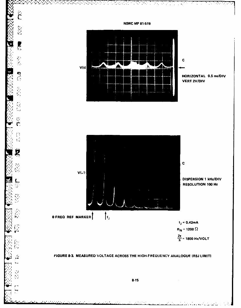
NSWC MP 81-519
~C
Vit) .. b ~. 4
A HORI ZONTAL 0.5 ms/DIV
MEN VERT 2V/DIV
C
L DISPERSION 1 kHz/DIVRESOLUTION 100 Hz
0 FREO REF MARKERt l
I j = 0.42mA
RN = 1200 ~2e
1800 HzNVOLT
* FIGURE 8-3. MEASURED VOLTAGE ACROSS THE HIGH-FREQUENCY ANALOGUE (RSJ LIMIT)
8-15
NSWC MP 81-519
Table 8-1 Numerical Interpretation of Figure 8-3
In the RSJ, current bias limit, the amplitude of the nt h harmonic of
the junction voltage at a particular IDC is proportional to (cf. sec. 2.4):
-(1)
!'- where y I/Ic!.*.,C
The Josephson frequency f j is related to y by- 1, (2)
From 8-7a, the Josephson frequency is measured to be 857 Hz. Using (2)
above, along with the values of I , R, and 2e/h from the figure, y is found
to be y= .727.
The relative amplitudes of the various harmonics of V(t) are found
from 8-7b to be approximately:
f 4.7X - Y (3a)
2f 2.1X - Y2 (3b)
3 fj .95X - Y3 (3c)
4f .45X - y4 (3d)
5f 3 .15X - y (3e)
where X relates the height of the spectral line in centimeters to its
corresponding voltage, and Y is defined in (1) above.
Combining (3a) and (3b), y is found to be y - .745 (compare with y - .727
above). Using (3a) again, X is found to be X - .095. Using this value of X,
rd th ththe amplitudes of the 3 , 4 , and 5 harmonics are .0903, .0428, and .0143.
Using y - .745, the corresponding values of Yn are .0893, .0399, and .0178.
The above cr .culations suggest that the high frequency analogue, when
operating in the RSJ limit, is producing results with an accuracy of 95% or more.
8-164
NSWC MP 81-519
LUsing equation 4-1 for the current through the analogue,'we have
I(V) = ImJ (V) + ReJ (V)sinO + imi 2 (V)coso
(8-8)
- dimJ2 (V)sinO - S(U - coso)ReJ 2 (V)
Note that to a first approximation, the phase shift error does not
affect the terms in Jl" However, it has the effect of mixing the real and
imaginary parts of J 2 "
The local oscillator provides two sine waves whose relative phase can
be varied continuously. It was found that with careful adjustment using a
PSD* and oscilloscope, there were no appreciable discrepancies in the
results obtained with the analogue that could be attributed to this source
of error.
8.7 Accuracy of the J and J2 Filters
The previous discussion has been concerned with what could be called
the "mainframe" of the analogue. The filters for J and J essentially1 2
plug into this mainframe, and for most applications can be considered
separately. This was done in the previous chapter, but with particular
emphasis on the design of filters for T # 0. In this section we continue
the discussion of filter design, but in terms of the T = 0 filters, and
with emphasis on how the accuracy of these filters affects the performance
of the complete analogue. Two problems are addressed. First, it is
important to know how well the electronic filters used in the analogue
model the response functions in the Werthamer theory. Second, the filters
in the analogue occur in duplicate pairs, and one must ask what happens to
the operation of the analogue if the actual response functions of a
particular pair are not identical.
*PSD: Phase Sensitive Detector
8-17p

?ISWC MP 81-519
The first of these questions is answered schematically in Figures 8-4
and 8-5, .which compare the theoretical expressions for J1 and J2 at T-O0
(in terms of the original elliptic integrals, and not the Pade approximates)
with the measured responses of the J 1 and 1J2 filters used in the analogue.
(These are rebuilt versions of the filters discussed in Chapter 4.) (A
comparison of the measured responses with theory for the filters for
T - .72T cand T - .9T cis given in Figures 7-5 and 7-6.) In Figures R-4
and 8-5, the agreement between the measured and calculated response is
good except in three respects. First, the Gibbs type overshoot at the gap
discontinuity is undesirable, particularly in the case of Im ill where it
can cause negative resistance problems (cf. Section 4.6). Second there
is some error caused by the inability of an electronic filter to model the
l/(abs f) behavior in the real parts of J1 and J2 at high frequency.
Third, the discontinuity in Im J.1 at the gap frequency should be equal to
the amplitude of the critical current. However, it is slightly higher,
with the result that photon assisted tunnelling steps will be slightly
larger with respect to Josephson steps than they should be. In terms of
computing the relative step heights of the Josephson and PAT steps as done
in the next chapter, this means that-the PAT steps should be nor-
V malized to the height of the discontinuity in Im J1 at the gap edge.
The question of how well one can match two filters for a particular
function for a given temperature is partially answered by Figures 8-6
10 and 8-7, which show a comparison of the measured responses of the
identical 1J1 and 1J2 filters for T -0. The main disagreement occurs at
the gap singularity, where high Q filters are used to model the Riedel
peak. The high Q biquads are more sensitive to slight errors in component
8-18

° rI
I'0:0
,,cn,. ,~., m9
i~C L 0
ZLIX
Ix 0 I-- LA-
cxcc:3c E u
o Ia I.. a..NLA
41 m0
N'AA
i1-19
• "uu

'0 '
z00 f0
(fU) U)
Ir t-
0. -
I.-.
92 I II-4 U)
0 cr.
V., /1NIA
3.20

F
NmCMP 31413
I a.
r
6~U
U.
-3
0
II.
II'U
=
V
FU
r
'I p
I I
NIA* .LAOA
641
a..
I
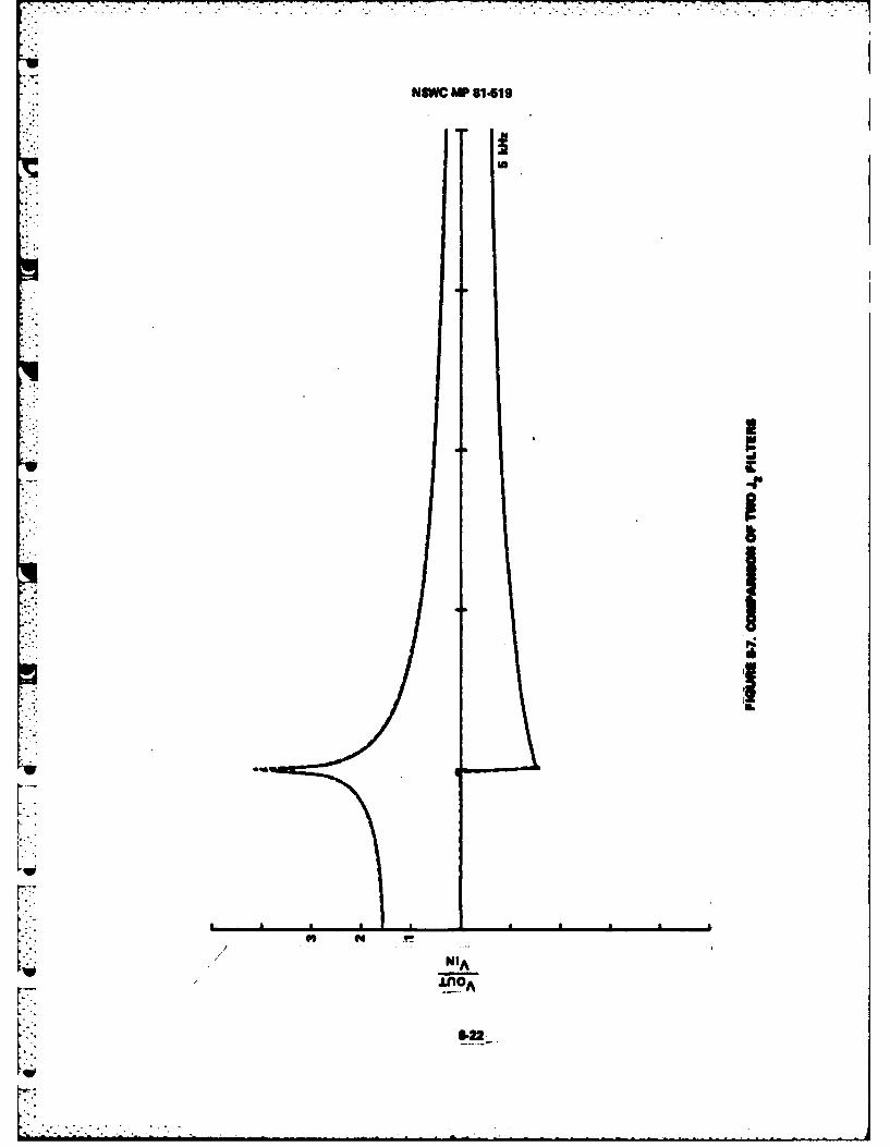
- . - - -
NSWC MP 61419
I.
U
U.IW
S
Ip.6
IV
[p
K / 0I NIA
3.22

NSWC MP 81-519
values than are low Q filters, and it is not surprising that the various
filters disagree. It should be noted that this disagreement can be
recd.-ced if painstaking care is used to match components for the high Q
biquads in each filter. This was not done when these filters were con-
structed; standard 2% components were used with no special attention given
to matching.
To estimate the quantitative effect of mismatch, it is interesting to
* calculate the effect of discrepancies in the two responses for Im Jon
the DC I-V characteristic of a voltage biased junction. Rewriting
equation 2-1 for the current through a tunnel junction in terms of non-
* identical J1 filters, we have:
12
I(t) - Im J + 6 sin 2wt - .sin 2wt (8-9)a r
wher Jaand Jb are the different Jl filters, and 6=Re J Re- b
6 Im J - ' b
We see that the effect of the mismatch is to average the two J 1filter
responses to get the DC response, and that there is an AC error term that
* is proportional to the difference between the two curves. Using numerical
data from the curves in Figures 8-6 and 8-7, we can calculate the DC
average and the error term in the region near the gap. This is shown in
Table 8-2. The error is noticeable, but there is little doubt that with
additional effort, the filters for J1adJ2 cnb ace etrta
they are now. Nevertheless, the results obtained with the analogue have
been quite good, and to a first approximation, this source of error can be
~ ignored. In the case of filters for nonzero temperatures, the Riedel peak
F* diminishes significantly, and the electronic filters do not contain
8-23

NSWC MP 81-519
Table 8-2 Utfect of a Mismatch Between the Measured Responses
of the J IFilters for T- 0
The two a, filters are designated Jr and Jb. F equation 2-1, we
have for the current due to ill
do-s d di dos
...(t) do (n.* Ja) " d2 ioo Jb)
In the voltage biased 1nit, */2 w yt. Letting Sr - me is- Re
-ban 'ii 10ja I b
1(t) In Ja + rSin 2wt " 1sin2wt
I(t) - In Ja - 41/2
For the 2 - 0, 31 filters used In the analogues
941 -.00 -.010 -.03 0
961 -.091 -.006 -.049 0
961 -.214 -.085 -.150 0[2 1001 1.483 .297 .890 1.57
1021 1.634 1.777 1.704 1.62
1041 1.647 1.714 1.662 1.66
-'The appropriate linear term has been added to Is ma and Im 3 b (m section
K-- 4.3)!i 8-24

F
NSWC MP 81-519
difficult-to-match high-Q biquads. As a result, the duplicate filters for
T # 0 match extremely well.
* . There is a final point that bears quick mention in this section. It
was reported in Chapter 4 that the overshoot in Im J for T = 0 at the gap
voltage could produce anomalous results, particularly if there was any shunt
capacitance across the junction. This overshoot is a direct consequence of
the use of a high-Q bandpass filter to model the step discontinuity in
Im J" Removing the relevant biquad would cure the anomaly, at a cost of
decreasing the ability of the analogue to model accurately photon-assisted
tunnelling steps. It is likely that some compromise could be reached, but
only at a cost of redesigning the entire filter. In the meantime, the
T - 0 filters were used with careful attention to any possible problems.
-. . In any event, adding some leakage current by decreasing the I JR. product
will provide a quick fix.
8.8 Preliminary Results
At this stage, we present some simple results obtained using the high
frequency analogue in the RSJ mode (e.g., with the filters disconnected.)
i fFigure 8-2 shows the time averaged I-V characteristics of the analogue
under current bias conditions, plotted against the theoretical solution to
the RSJ equation. The agreement is relatively good, although it could
probably be improved by giving more attention to the various calibration
step. (e.g., adjusting DC offsets and the relative phase of the VCO and
LO, etc.). However, the major disagreement between experiment and theoryr
. may well be due to scaling and plotting difficulties. The choice of
R. - 1280 ohms for the theoretical calculation did not take into account
the possibility of non-infinite source impedance, which would lower the
8-25

.NSWC !'W 81-519
effective R jof the analogue slightly. Also, the superposition of the two
graphs was done in an ad hoc manner using two different plotters, and the
zero voltage steps are not precisely aligned.
Figures 8-3a and 8-3b show photographs of the voltage as a function of
time for a particular value of current, as veil as a photo of a spectrum
analyzer display of the voltage. Comparison of several photos taken at
different values of Icindicates that the harmonic content, as well as the
variation of the amplitude of the fundamental component with DC current,
agree with the theory. Any significant errors would be expected to
show up either as amplitude errors, or by the appearance of spurious
spectral lines. A numerical analysis of Figure 8-3b is given in Table 8-1.
Figures 8-8 and 8-9 are a retake of the impedance data shown in
Chapter 3 for the 383 analogue. The data presented here was obtained
with the simple AMJ analogue (not the high frequency analogue in the 383
mode). However, the low pass filter consisted of a twin-T with a center
frequency of 100 kWz, and an equivalent cosine phi amplitude of -. 031.
The data is plotted against the results of the theoretical calculations
of Auracher and van Duzer. This was done by digitizing graphs from their
original publication, and having a desktop computer plot them on top of
the results obtained using the analogue. The level of agreement is roughly
the same as that in Figure 8-2 for the DC I-V curves of the high frequency
analogue operated in the 383 mode. The close agreement between the
* theoretical and simulated curves indicates not only that the junction
impedance varies as predicted, but that the measured step heights agree
with theory as well. The major disagreement seems to be within the zeroth
* order step. The effect of the unwanted cos phi term immediately comes to
mind, but this has yet to be investigated. (As the analogue is being
8-26

NSWC 141 81-519
cc
UA
IcU. cc
lu 0Zz
us 0
ILUI
I--. 8-27

KS1C MP 81-519 1
AML
P9
0U
w aa
8-28
.. ....

NSWC M4P 81-519
operated in a high-signal limit, the small-signal theory of Chapters 3
arnd 6 does not apply.)
In the time since these measurements were made, some improvements have
been made to the PSD measuring techniques, and to the analogue itself, and
it seems likely that these results could be improved somewhat. Given the
-. constraints of time, this has not been done.
At this stage, the results to be presented begin to fall more into
the category of using the analogue, and less into the category of testing
it. The discussion will be less in terms of electronics, and more in
term of the physics of the Josephson effects. To emphasize this
philosophical transition, the remainder of the results are organized
into a separate chapter.
L
8-29/8-30

NSWC MP 81-519
CHAPTER 9
FURTHER RESULTS
9.1 Introduction
FWith the improvements described in the previous chapter, it became
possible to use the analogue to quantitatively model a wide range of
experiments. In this chapter, results are presented which illustrate the
performance of the analogue in a variety of experimental situations.
Where possible, these results are compared with theoretical calculations,
and with experimental data obtained from real junctions.
The discussion begins with a presentation of current-voltage
characteristics obtained with the analogue using the various filters
under different bias conditions. These results illustrate the temperature
dependence of the energy gap, Riedel peak, and quasiparticle resistance.
-Next is a comparision of analogue data with the step height calculationsr21
published by Hamilton. To the author's knowledge, this is the first time
an electronic analogue has been used to measure the properties of photon-
assisted tunnelling steps.
[This is followed by measurements of the Q of the plasma resonance
versus frequency in the RSJ and T - .72T limits. The results support thec
prediction made in chapter 6 that the nonlinearity of Im J can have a
major effect on the Q of the plasma oscillations.
F Then there is a brief discussion of the effect of series inductance
on the dynamics of a voltage biased junction. It was found that the
L inductance permits parasitic oscillations to occur when the analogue is
biased in the region behind the Riedel peak. These oscillations appear to
L4 be responsible for the ancmalous broadening of the Riedel peak reported in
Chapter 4.
9-1
NSWC MP 81-519
Lastly, an explanation is offered to explain the apparently anomalous
sub-gap structure observed in some of the measured I-V characteristics
of the capacitively shunted analogue.
9.2 Current-Voltage Characteristics at Various Temperatures
Figures 9-1 and 9-2 show the time averaged I-V characteristics of the
analogue with the various filters connected. 'In Figure 9-1, the analogue is
voltage biased, and the curves represent Im 13 as a function of voltage for
T - 0, T - .72T c, and T - .9T c, its well as for the RSJ limit, where the
characteristic is just that of the resistor connected in parallel with the
analogue. Except for switching in the various filters, no adjustments were
made to the analogue, the drive circuitry, or the plotter between the
different measurements. The agreement between Figure 9-1 and the Werthamer
theory is quite good. Note how the gap voltage decreases and the leakage
current increases as the temperature is reduced. The relationship between
gap voltage and temperature is that given by the ECS theory, which is built
into the Werthazer theory.5
The spikes at zero voltage in Figure 9-1 are caused by the J2 filters,
which were left connected for the experiment. It was found that if the
analogue is left very near V - 0, the plotter pen will oscillate between
+I J and -I * This is simply the oscillation of the supercurrent at the
Josephson frequency. For large voltages, the Josephson oscillations are
rapid enough to be eliminated by the low pass filters used to average
V and 1. As V approaches zero, the Josephson frequency is small enough to
be passed by the filters, and the oscillations are slow enough that the
servos in the plotter can trace them out.* In Figure 9-1, the voltage

NSWC !4P 81-519
T flmAInh)
RSJ
* FIGURE 1-1 I-V CHARACTERISTICS OF VOLTAGE BIASED ANALOGUE AT DIFFERENT TEMPERATURES
9-3

NSW~ mp 81-519
T-
FIGURE 9-2 1V CHARACTERISTICS OF THE CURRENT BIASED ANALOGUE AT DIFFERENT TEMPERATURESL-

NSWIC MP 81-519
is swept too rapidly for this to occur to its full extent, but in later
experiments, this effect was used to measure the heights of the Josephson
steps.
~:; rFigure 9-2 illustrates the effect of current bias. No adjustments
were made to the analogue or plotter between plotting Figures 9-1 and 9-2.
A single switch is used to change the external bias circuitry from a
voltage source to a current source. Note how the critical current, as vell
as the gap voltage and the height of the Riedel peak, decrease with
increasing temperature. However, the normal state resistance remains
constant.
Figure 9-3 is a prelude to a comparision of analogue results with21
data published by Hamilton. The figure shows the effect of "microwaves"
rh at 82.*4 Hz on the current and voltage biased characteristics of the
analogue with the T - 0 filters connected. (82.4 Hz in the analogue is
equivalent to 23.4 G~z in a tin tunnel junction.) The current biased
characteristic illustrates the hysteresis and smearing effects discussed in
chapter 4. Upon switching to voltage bias (the characteristic is reversed
in the figure to separate it from the current bias case) the characteristic
- is much more stable. The Josephson steps appear as spikes centered about
* V - 0, and the photon-assisted tunnelling steps appear as steps centered
around the gap voltage. Note that the Josephson steps are spaced twice as
closely as the PAT steps, as predicted by theory (cf. Chapter 5).
in switching from current to voltage bias, the RP source went from
providing .75mA p-p to providing .75V p-p. If the analogue was in the
RSJ limit and the junction resistance was 1000 ohms, then the voltage at the
input to the analogue would have approximately the same amplitude (although
9-5

NSI 14P 81-519
II
I-
0 V,a.c
6 0
9-6-

NSWC NP 81-519
different harmonic content) in each case. (In the example shown, the
normal state resistance is 1150 ohms.) However, when the T - 0 filters are
used, the RP resistance at frequencies below the gap frequency will be
considerably greater than R J(cf. eqn. 2-25 and 6-12), and switching from
voltage to current bias without adjusting the bias amplitude will cause a
big change in the RP voltage at the input to the analogue. Thus, when the
analogue is biased at frequencies below the gap frequency 2A/h, switching
* from voltage to current bias can be expected to cause a substantial change
in the RF impedance and the step heights.
A similar effect occurs if the analogue is current biased at an RF
frequency below the gap frequency 2A/h, and the analogue is switched from
the RSJ to the T -0 limit. in this case, the large increase in the quasi-
particle resistance below the gap frequency causes a large change in the
input- voltage, and hence a large change in the RF impedance and step heights.
On the other hand, if the frequency of the WI bias is greater than the
gap frequency, switching in the T - 0 filters does not cause a dramatic change
in the amplitude of the R? voltage for a given level of FS current bias.
Thus, if the applied frequency is greater than 2A/h, switching from the RSJ
* to the T - 0 limits would not be expected to cause as dramatic a change in
the RP impedance of the analogue as when the applied frequency is less than
2A/h.
* ~ This helps explain an apparent anomaly in the impedance data presented
in chapter 4. The impedance was measured at a particular level of RP current
* bias with the analogue in the RSJ limit. The T - 0 filters were then
* ,. switched in, but the 1W input current was left unchanged. Figure 9-4 shows
* * this for an applied frequency of .4 times the Josephson frequency 2eIJR/h
9-7

RESISTANCEO
REACTANCE
FIGUE 94HIGHFREQENCYISTEANCEI
CD
.09-8
WETAE

NSWC MP 81-519
P (cf. Fig. 3-12). The Josephson frequency is w/2 times the gap frequency,
which means that .4 f is less than 2A/h. Note that there is a substantial
change in the RP impedance in the two limits.
Upon further investigation, it was found that if the RP bias level was
scaled downward to compensate for the increase in the quasiparticle resist-
ance, the impedance became similar to the original impedance measured in the
RSJ limit (e.g. - inductive instead of capacitive in the zeroth order step).
Conversely, it was found that at certain bias levels the impedance in the RSJ
limit will be capacitive, instead of inductive, in the zeroth order step;
_ - thus, the capacitive reactance shown in Figure 9-4 is not a unique consequence
of the Werthamer theory. Furthermore, it was determined that in the high
frequency limit, switching off the Jl filters (e.g. - lowering the RP quasi-
particle resistance) had approximately the same effect as reducing the RP
current.
Figure 9-5 offers further evidence to support the above argument.
In this case, the frequency of the applied RP is equal to the Josephson
frequency, and hence greater than the gap frequency. As the analogue is
switched between the RSJ and T - 0 limits, the change in the R? impedance,
particularly in the zeroth order step, is much less drastic than that shown
-"in Figure 9-4.
9.3 Simulation of the Hamilton Experiments
Hamilton has performed a series of experiments directly aimed at verify-
*ing certain aspects of the Werthamer theory, most notably the frequency
dependence of ReJ 2 , 21 Using frequencies in the 25 GHz range, he measured the
power and frequency dependences of the Josephson and photon-assisted tunnell-
ing steps in tin tunnel junctions. His results, which were compared with
9-9

NSac mI 81-51i
RSJ
RESISTANCE
IC
DIRECTION~OF CURRENT
REACTANCE. ;SWEEP
WERTIIAMER
w
FIGURE~ "tHIHREClUENCYIMPEDANClE Il-
9-10

NSWC MP 81-519
theoretical calculations, offer strong support for the Werthamer theory.
As 25 GHz is only a small fraction of the gap frequency 26/h of 284
GHz for tin, most of the high frequency corrections to the RSJ model were
quite small, and required extremely careful measurement to be observed. For
this reason, an electronic simulation of Hamilton's experiments proved to be
a challenging test for the electronic analogue. In this section, we describe
the results of this test.
Hamilton's data was obtained by measuring the time averaged I-V
characteristics of tin tunnel junctions under DC current bias conditions.
r- Although the junctions were small (10 - 6 2 ), their capacitance was presumed
sufficient for the microwave radiation to be treated as a voltage source.
This assumption, which was validated by the close agreement between experi-
ment and calculation, greatly simplifies theoretical calculations.
Figure 9-6 shows two I-V characteristics obtained using the analogue
with the T - 0 filters. The first curve was obtained with the analogue volt-
age biased with a DC and an RP signal. Both the R? frequency and the RP
voltage are scaled to the levels used in Hamilton's experiments. The second
curve shows the analogue under current bias conditions, but with a 4 micro-
farad capacitor across the input. This value was scaled to the estimated
capacitance of Hamilton's tin tunnel junctions. Comparison of the step
heights in the two cases suggests that Hamilton's assumption that the
capacitance causes the junction to look voltage biased at high frequencies
is valid. Examination of V(t) on an oscilloscope indicated that harmonics of
the applied RP frequency were observable until C was increased to approximately
10 microfarads. However, at C = 4 microfarads, the harmonic distortion was
only about ten percent. In a real junction, the microwave source impedance
9-11
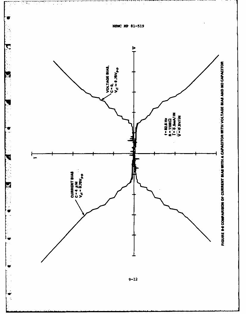
z I-
.8102
IC* c
9-1-
- -- ---- ---

NSWC MP 81-519
in the absence of a capacitor is unlikely to be as high as the source
impedance of the current source in the analogue. Thus, Hamilton's assumption
is probably more valid for a real junction than it is for the case described
above.
Because of the existence of supercurrents, the relationship between the
applied WF current and the RF voltage across the analogue was extremely non-
linear at low values of RP current. This made it difficult to accurately
adjust the voltage across the analogue by varying the current. In addition,
it was found that the I-V characteristics under current bias conditions were
often unstable, and exhibited much hysteresis, sub-gap structure, and
complicated interactions between photon step. and Josephson steps. Further-
more, when capacitance was added, half harmonic steps began to appear. (The
appearance of h~lf -harmonic structure when there is shunt capacitance is
predicted by the RSJ model. It its not surprising to observe it in the high
sofrequency model as well.) The net result of all this is that the current
biased characteristics are quite complicated and difficult to interpret,
whereas the voltage biased characteristics behave in a relatively simple
and predictable manner. For this reason, it was decided to simulate the
Hamilton experiments using the analogue with a voltage source and no
capacitance.
In Figure 9-6, the Josephson steps show up as spikes whose heights could
be measured by changing the voltage very slowly, and allowing the plotter to
sweep out the Josephson oscillations as f became very small. To make sureJ
that the spikes were fully traced out, 50 ohms of series resistance was added
to the voltage source. This reduced the slope of the load line which traces
out the spike, and ensured that the current at a spike didn't change too
9-13

NSWC MP 81-519
rapidly for the servo motors in the plotter to respond. It was verified that
the 50 ohm resistance has a negligible effect on the amplitude and harmonic
content of the input voltage. It might be noted that the change in the spike
shape upon introduction of the additional 50 ohms indicates that the original
output impedance of the voltage source is quite small. Some typical current-
voltage relationships obtained in this way are shown in Figure 9-7. Note
that the supercurrent Josephson spikes, which depend on Re J2 ' are quite
different from the photon-assisted tunnelling steps, which can be looked
upon as images of the discontinuity in Im J1 " Most of the data on step heights
was obtained from plots such as those in Figure 9-7,
Before presenting any further results, it is useful to review some
aspects of the Werthamer theory that are relevant to the measurement of step
heights. Equations 9-1 and 9-2 show the theoretical expressions for the DC
current at a step for the cases of pair tunnelling and quasiparticle tunnell-21
ing, respectively. Equation 9-3 shows the expression for the DC current of
a Josephson step in the RSJ limit. (There are no PAT steps in the RSJ limit.)
I d (V dc It I Y (a) J Nn(G)RGJ2 ((2n - N)f)I 6(V d + Nhf/2e) (9-1)
dc d dc)mn n 21o
-U
Idc(Vdc) - ReJ 2 (0)IJN (2a)[6(Vdc + Nhf/2e) (9-3)
U where delta is the Kronecker delta function, and a - eVrf/hf-9-1
. 9-14

NSWC NP 81-519
9. CL
CLF
LU
U,
0w
04
'I
II 0
9-1-

NSWC MP 81-519
Note that the Josephson steps occur at Vdc - Nhf/2e. The photon-assisted
tunnelling steps occur when the argument of Im J1 is equal to 2f/e, which is
when Vdc = A/e + nhf/e).
The above equations are obtained by letting the junction voltage -
Vdc + Vrf cos 21ft and solving for the current using equations 2-1 and 2-4.
Note that the step heights in the high frequency case are proportional to J 2(a)q n
as opposed to J (2a), as predicted by the RSJ theory.* This results from then
use of the quantities sin /2 and cos /2 in the Werthamer theory, instead of
sin 0 and cos * as in the RSJ theory. If the amplitude of Re J2 and theW2
slope of Im Jl are treated as being constant, then the summations in 9-1 will
converge to that of 9-3. Because there is no discontinuity in Im J1 in the
RSJ limit, the PAT steps disappear.
The photon-assisted tunnelling steps are readily apparent in the measured
characteristics of the analogue. However, the effect of the Riedel singularity
on the heights of the Josephson steps is minimal until large values of alpha
are reached. This is shown in Figure 9-8a, where Hamilton has used equations
9. 1 and 9-3 to calculate the variation of the height of the N = 0 Josephson21
step as a function of input power for both the RSJ and Werthamer cases.
Note that no differences are observed until the seventh zero of the step
height has occurred.
Figures 9-8b and 9-8c show results obtained with the analogue in both the
RSJ and T - 0 cases. The horizontal axis corresponds to the RF voltage, as
measured with a lock-in amplifier. The vertical lines were obtained by
letting the plotter pen oscillate for several seconds as the analogue remained
biased in the zeroth order step. The 50 ohm source impedance was deleted, and
a- eVrf/hf 9-16

NSWC MP 81-519
1.0
-- WERTHAMER THEORY
---.. RSJ
Lu
= =0.5CL N-0I-
oo2 -0 10 20 30 40 50
9-4a. THEORETICAL PREDICTION (AFTER HAMILTON5 9 )
' " 2s. Vff
- 1800 Hz/VOLT cx - f 90 Hzhf
VRF lVp.p 2 Vp.p 3Vp.p 4Vp.p
m-
9-8b. ANALOGUE IN WERTHAMER LIMIT, T -0
* VRF 1Vp 2Vp 3V 4V
I1111i I .1i I , liJi ~ i*l..lll..,l ..,ll,.,,ll. if .,, l 'Ii'm,
94hc. ANALOGUE IN RSJ LIMIT
FIG. 94 VARIATION OF N -0 JOSEPHSON STEP WITH R-F VOLTAGE
9-17

NSWC MP 81-519
the measurement of the step height is relatively inaccurate. However, note
the good qualitativ, agreement between the analogue and calculations based on
equations 9-1 and 9-3, particularly in the 2 to 4 volt region.
The VCO gain constant of the analogue was such that e/h was 900 Hz/volt.
The dimensionless quantity a - eVf/ (hf) scales quite well between the
analogue and Hamilton's calculation. The difference in relative step heights
between the T - 0 and RSJ limits is a fact or of ir/2, which is the DC gain
of the J 2 filters used in the analogue. (Removing the J 2 filters for the
RSJ case lowers the critical current by this amount.)
Figure 9-9a shows the height variation of the N - 3 Josephson and the
n - 3 PAT steps, as calculated by Hamilton using equations 9-1 and 9-2. The
circles are experimental points obtained by Hamilton using a tin tunnel
junction at 1.3K with applied RF at 23.5 Q~z. Note that Hamilton was only
able to obtain data for large values of a for the N - 3 Josephson step, and
small values of a for the n - 3 PAT step. The former limitation resulted
from hysteresis in the current biased characteristic at low power levels,
which made some of the Josephson steps inaccessible to measurement. The
latter restriction arose from the problem of Josephson steps obscuring the
PAT steps at large values of RF power. (As the RI' power is increased,
Josephson steps begin to appear away from V M 0, whereas PAT stepsdc
begin to appear away from Vd M 2,&/. Eventually, the two interfere with
each other.)
Neither of the above restrictions applied to the analogue. As the
analogue was voltage biased, hysteresis wasn't present. When the Josephson
*spikes started interfering with the PAT steps, either the J 1 or J 2 filters
could be temporarily disconnected. (Note that equations 9-1 and 9-2 are
completely independent. In the voltage biased limit, disconnecting one set
9-18

NSWC MP 81-519
0.4 o - TUNNEL JUNCTION - 235 GHzT - 1.3*K
0 .10 20 30 40 5 0/ 2sVrt hf
0.2 - Vrf - 2 A/,
(a) n - 3 QUASIPARTICLE STEP
00
0
0 5 10 is 20 - 25
(b)
f - 23.5 GHz~T ,, 1.3°K0.4 X -ANALOGUE
x N - 3 JOSEPHSON STEP
x
b. 0 10 20 30 40 - 0
0.2- Vrf 24 lo 2Vr/hf
"-- (a)
n - 3 QUASIPARTICLE STEP
x
0 . 10 15 20 -. 25I eVrf/hf
p (b)
FIGURE 9-9 VARIATION OF N , 3 JOSEPHSON AND n 3 PAT STEPS WITH R-F POWgR
(AFTER HAMILTON) 2 1
9-19
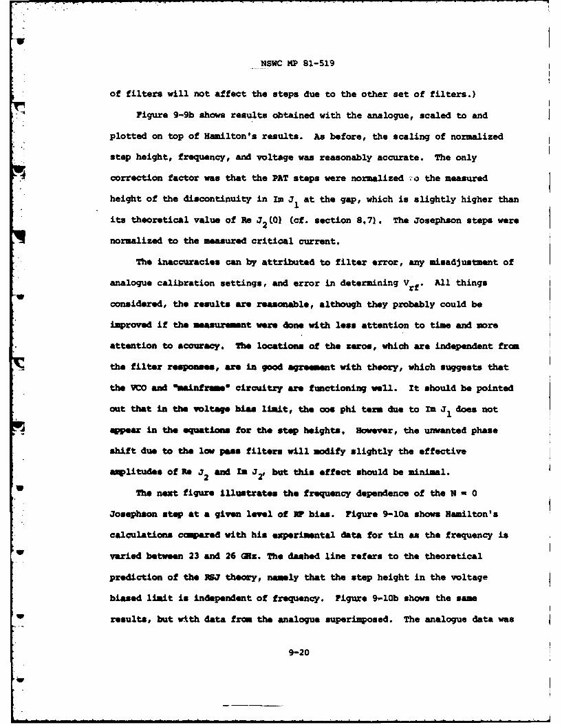
NSWC MP 81-519
of filters will not affect the steps due to the other set of filters.)
Figure 9-9b shows results obtained with the analogue, scaled to and
plotted on top of Hamilton's results. As before, the scaling of normalized
step height, frequency, and voltage was reasonably accurate. The only
correction factor was that the PAT steps were normalized :o the measured
height of the discontinuity in Im J at the gap, which is slightly higher than
its theoretical value of Re J2 (0) cf. section 8.7). The Josephson steps were
normalized to the measured critical current.
The inaccuracies can by attributed to filter error, any misadjustment of
analogue calibration settings, and error in determining Vrf* All things
considered, the results are reasonable, although they probably could be
improved if the measu t were done with less attention to time and more
attention to accuracy, The locations of the zeros, which are independent from
the filter resposes, are in good agreement with theory, which suggests that
the VCO and *mainframe* circuitry are functioning well. It should be pointed
out that in the voltage bLas linit, the 006 phi term due to In J does not
appear in the equations for the step heights. However, the unwanted phase
shift due to the low pass filters will modify slightly the effective
amplitudes of Re J2 and In J2 but this effect should be minimal.
The next figure illustrates the frequency dependence of the N - 0
Josephson stop at a given level of 1W bias. Figure 9-10a shows Hamilton's
calculations compared with his experimental data for tin as the frequency is
V varied between 23 and 26 G~z. The dashed line refers to the theoretical
prediction of the Ps theory, namely that the step height in the voltage
biased limit is independent of frequency. Figure 9-10b shows the same
results, but with data from the analogue superimposed. The analogue data was
9-20
iw
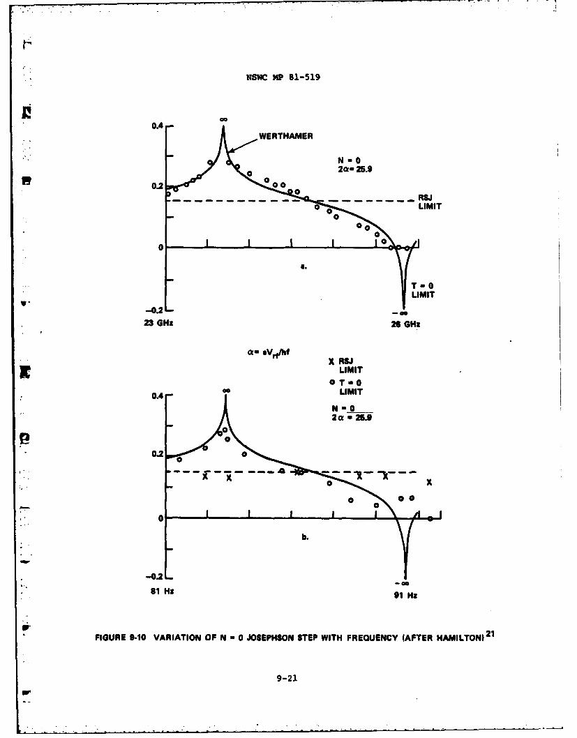
NSWC 1l@ 81-519
0.T-O
0 Gci-225.9
LIMITIN0
-~ 25.9
23 1H 261Hz
p. ve ~ SFIGUE 9.0 VAIATON O N -0 JSEPHON SEPIFEUNCIATRHAITNT
9-21-

NSWC MP 81-519
obtained by varying the frequency from 81 to 91 Hz at a particular level of
RP voltage. The measurement is very sensitive to slight variations in Vrf
and misadjustment of Vr is probably the prime source of error. (Note that
Hamilton's calculations allow for negative step heights; the absolute value
should be taken-as shown in 9-l0b.)
The last figure in this section (Fig. 9-11) is a comparison of an I-V
characteristic calculated on a desktop computer with a measurement done using
the analogue. The analogue measurement is presented both separately and as
an overlay to the digital computation. The J2filters were disconnected, and
the analogue was voltage biased. Using equation 9-2, it took the Hewlett-
Packard 9835 system several hours to calculate the curve. The analogue
completed the measurement in less than 15 seconds.
As it stands, the results presented above could almost certainly be
improved. However, it was decided not to dote on the measurement of step
heights, but to proceed with measurements of the plasma resonance using some
of the finite temperature filters.ME
9.4 The Plasm Resonance
The improvements to the analogue described in the previous chapter,' as
*well as the availability of improved measuring equipment, made it worthwhile
to repeat the plasm resonance experiments discussed in Chapter 4 (cf. Fig. 4-32
and 4-33). The experimental setup is relatively simple, and is outlined in
U Figure 9-12. The analogue is shunted with a capacitor, and current biased
within the zeroth order step. At low input levels, the device behaves as a
parallel PLC network whose inductance is determined by the equilibrium value
W of cosine phi, which in turn is determined oy the DC current. A frequency
response analyzer (FMA) is used to generate the AC current. The voltage at
9-22
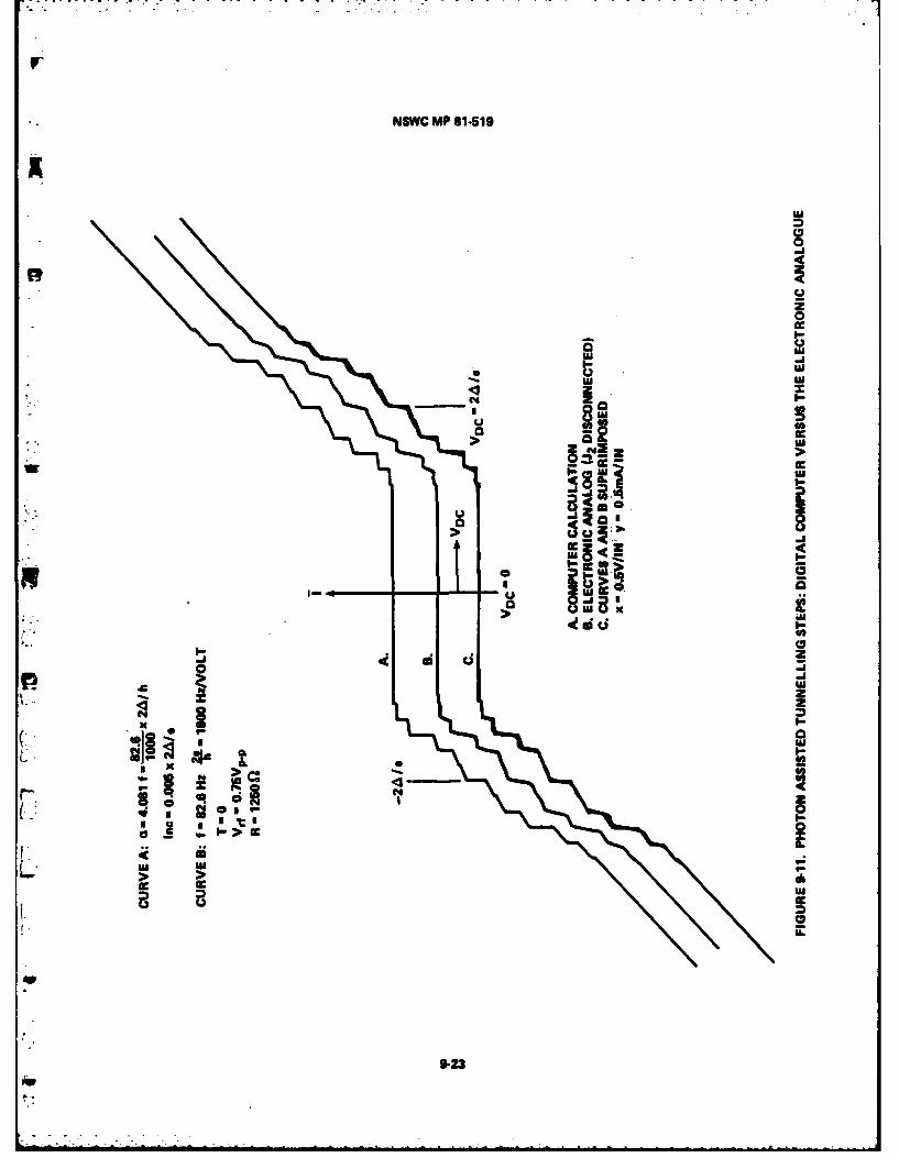
NWC MP 81519
Bz z0
S U &
4 2 z
o U
Z d z0 iI-
d I-
a j 4 UI-
>2
o >I
9.2APa

NSIC lIP 81-519
'Uc
I 4
'Uu
cc C
CJ IL
3 w=
ui g-3 I>
aJ z
LW'U
zac 4i 44
ccU... 1
9-24.

NSWC MP 81-519
the input to the analogue is returned to the FRA, which measures its amplitude
and phase relative to the current. This information is stored in a desktop
computer, and is processed upon completion of a series of measurements.
The first experiments were done using a simple RSJ analogue containing a
twin-T filter. Typical results are shown in Figure 9-13, which shows the
impedance as a function of frequency for several values of cosine phi. At
resonance, the height of an im ped ance curve in Figure 9-13 is proportional to
the resistance. In the figure, a height of 1 corresponds to R - R * When the
height is greater than 1, as is the case for large values of cos phi, it
means that the negative cos phi amplitude is causing the apparent value of
the junction resistance to increase. Since Q w RC, the amplitude of the
impedance at resonance is proportional to the Q.The variation of R with
cos phi is given by-
LrR - Rj/(l + Ycos#) (9-.4)
This curve is plotted for y - -.057 as the envelope containing the maxima
of the curves for the real part of the impedance. This represents a "best
fit" to the data. However, the predicted value of gamm was -.031. This was
verified by independent measurement of the low pass filter response. It
turned out that the cumulative phase shift of the remainder of the analogue
was responsible for the remaining contribution to gamma.
To emphasize the effect of a negative cos phi amplitude on the impedance
of the analogue, the low pass filter was replaced by a filter having a relative
cos phi amplitude of -.83. The effects of this are illustrated in Figure 9-14.
Note that for cosine phi - 1, the junction's resistance is almost six times
as great as R. An envelope to the impedance maxima based on a value of
9-25

Ns1c NP 81-519
R Y10.5
@os 0.0.660 U0.9 1 i . cos~'
1.0 - - - - - - - - - -4+
130 Hz
FIGURE 9-13 IMPEDANCE VS FREO FOR THE RSJ ANALOGUESHUNTED BY A CAPACITOR (SMALL-SIGNAL LIMIT)
9-26

NSWC Hp 61-519
6 DECREASING Q
5
4I
3 R 1i
-3
-4
FIGURE 9-14 EFFECT OF LOW PASS FILTER ON 0 OF PLASMA RESONANCE
9-27

NSWC MP 81-519
gaa --. 88 is plotted in the figure. Note that as cosine phi goes to zero,
the junction resistance approaches R.. The difference between the predicted
gaa of -,83 mid the value of -. 88 can be attributed to a combination of
extra phase shift contributions in the circuit, and conservatism in fitting
the envelope curve.
Measurements of the Q of the resonance curves from the bandwidth of the
impedance curves are consistent with measurement of Q from the resistance of
the analogue at resonance, These results are summarized in Table 9-1.
The above measurements were repeated using the high frequency analogue
with the T - . 72T cfilters at a nom~inal plasm frequency of 500 Hz. At this
frequency, the cos phi amplitude is small (approx. + .026), and is expected
to have relatively little effect on the apparent resistance of the analogue.
The measurements were first made using only the J 2 filters, so that the shunt
resistance was constant, independent of frequency. The experiment was then
repeated with no changes except to connect the Jfilters to introduce a
frequency dependent value of shunt resistance.
Figure 9-15 shows the I-V characteristics of the analogue in the
T - .72T mode with both Jand i connected, with and without capacitance;c 1 2
and with only the J2filter connected, with and without cxpacitance. The
voltage biased limit, with both iland J 2 connected and C - 0, is also shown
to illustrate the variation of Im J1with voltage (and frequency).
Figure 9-16 shows the variation of impedance with cosine phi with the
1filters disconnected. Note the small variation of the impedance at
resonance with cos phi. This indicates that the effect of the Im J2cos phi
amplitude is minimal, as expected. In this and the next figure, the vertical
axis is scaled in units of 1000 ohms. The amplitudes of the maxima are
9-28

NSWC MP 81-519
TABLE 9-1 F AND F /Q FOR THE RSJ ANALOGUE FOR TWOp p
DIFFERENT VALUES OF COS PHI COEFFICIENT
Vin(rms) cos phi Fp(meas) Fp(predl Fp/Q(meas) Fp/Q(pred)
With only a Twin-T filter:
(Fp/Q(pred) is calculated using gamma - -. 03)
.05 1 236 237.7 45 45.3
.015 .9 225 225.5 46 45.4
.025 .9 225 225.5 44 45.4
5 .05 .8 210 212.6 46 45.6
II .05, .66 187 193.1 46 45.8
.025 .5 168 168.1 46 45.0
With the addition of a low pass filter:
(Fp/Q(pred) based on gamma -. 83)
I .015 1 230 237.7 8 7.9
[ .025 1 226 237.7 9 7.9
.015 .9 220 225.5 11 11.8
.015 .8 208 212.6 15 15.7
.015 .66 190 193.1 24 21.1
.015 .5 168 168.1 24 27.3
(Note, the measurement of F /Q with the LPF connected is suspect,as some of the curves were showing non-Lorentizan behavior, andit was not always obvious what value should be used for the halfpower bandwidth.)
9-29

NSWC MP 81-519
4
Q cc I--
Io N
00
U
I.-
IC
U-U
UIA
I-n
zU
zC0
z
z 0ccU
9-30
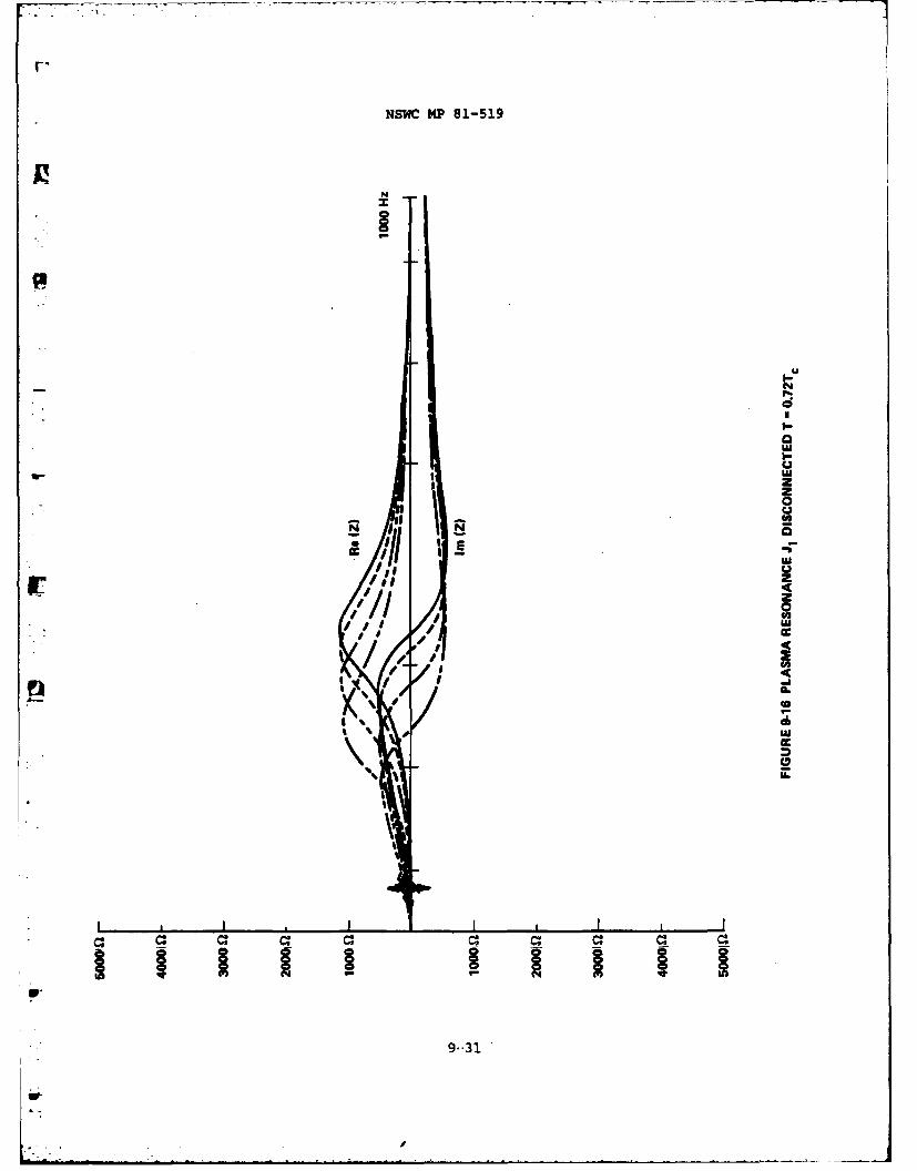
NSWC MP 81-519
zz
z
0UAc-
I-
LUU- I cc
c! C C: : C: a C: C: C
9-31
.... ... ...
UI
NSWC MP 81-519
consistent with the value of shunt resistance of 1150 ohms.
Figure 9-17 shows the same measurement, but with the J filters
connected. Note the large increase in the apparent resistance of the
analogue, as well as the strong .frequency (as opposed to cosine phi)
dependence of the amplitude and bandwidth of the resonance. (The interference
at 60 Hz and its multiples is mains pickup.) The discussion in section 6.4
explains this dependence, and its similarity to the effect of a negative cos
phi amplitude, in terms of the frequency dependence of Im Jl" A quantitative
analysis of the data in Figures 9-16 and 9-17 is shown in Table 9-2.
* There is good agreement between the above results and the theory
described in Chapter 6 for the effect of Im J on the plasma resonance. The
particular choice of parameters, in terms of temperature, frequency, junction
resistance, and capacitance, represents a situation that should be realizable
using real tunnel junctions.
The above experiment, if repeated using tunnel junctions as described
in section 6.6, would confirm the relationship between Im J1 V), as measured
from the current-voltage characteristic of a junction, and Im J1(f), which
determines the resistance of the junction at microwave frequencies. Addition-
ally, the experimental results could shed considerable light on the still
unresolved cosine phi controversy.
In other experiments done to measure the relationship between the
quasiparticle conductance (Im J1 ) and the cos phi term (Im J 2) , the frequency
is generally fixed (cf. Chapter 6). The above experiment, however, would
investigate the frequency dependence of these terms, and thus yield information
of considerable inportance in verifying the accuracy of the Werthamer theory.
Furthermore, performing measurements at more than one frequency would aid in
9-32
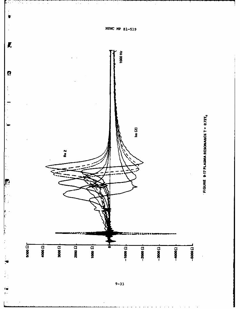
U
NSWC HP 81-519
N
UI-
- I-wU220U,w=
U0)
-Ja.g~.I-
w=C,
C-
t - -
1~
9-33

NSWC MP 81-519
TABLE 9-2 PLASMA RESONANCE, T .72 Tc
a. J FILTERS DISCONNECTED, Ij = .45 mA (measured)
2e/h - 1800 Hz/volt R - 1150D
C - .81ufd (measured)
cos_ 0 f (theor) f (meas) R (theor) R (meas)
1 399 405 1150 1153
.914 381 380 1150 1139
.785 353 335 1150 1116
.475 275 275 1150 1086
b. 1 FILTERS CONNECTED, Ij - .43 mA (measured)
2e/h - 1800 Hz/volt R - 1150
C - .81ufd (measured)
cos #0 f (theor) f (meas) R (theor) R (meas)p P
1 391 400 3500 3923
• .88 367 375 3336 3582
.81 352 360 3306 3421
.63 311 315 3125 3106
* .46 265 260 2833 2828
2e1I OBTAINED FROM A MEASUREMENT OF24w f- co Im J1(V), T - .72 T
p~ _M lii (f)
f - eV/h
9-34

NSWC MP 81-519
the elimination of spurious data.
9.5 Anomalous Broadeninq of the Riedel Peak
To conclude this chapter, we discuss further observations of the effect of
* series inductance on the performance of the analogue in the voltage biased
limit. With the T - 0 filters, it was found that the shape of the back of the
Riedel peak could be observed. (In the current biased limit, this region is
* inaccessible). However, as the inductance was increased, the Riedel peak became
- broader and higher than predicted by the shape of Re J(cf. Figures 4-17 and
4-18).
Observation of the junction current and voltage indicated that the negative
slope of Re J2behind the Riedel peak was causing a com~plicated series of
oscillations. Figure 9-18 shows this anomalous broadening of the Riedel peak#
along with the tine dependent current and voltage at various bias points.
In qualitative terms, it appears that the negative slope of the I-V
characteristic behind the Riedel peak causes the bias point to drift towards the
gap singularity when the analogue is biased at DC voltages slightly greater than
2A/e. A small decrease In voltage causes a slight increase in current, which
causes an additional decrease in voltage, and so on.
The analysis of the problem is complicated by the different time scales
involved. At any instant, the Josephson oscillations appear to satisfy an
instantaneous version of the 883 equation. That is, the individual oscillations
in the photographs in Figure 9-18 look like those predicted by the RBJ model for
particular values of I 3 and RN. However, the frequency, amplitude, and DC
offset of these oscillations vary in a time frame that is slow relative to an
individual Josephson oscillation (e.g., one over the gap frequency), but quite
fast relative to the time constants associated with measuring the DC I-VFlo
characteristic.
9-35

NSW~ M 81-519
a we
N.0
aj
01I-Z
mu 0
-N-
>mos 1*
'U I
9-36

NSWC MP 81-519
Measurement of the Josephson frequencies from Figure 9-18 indicates that
the oscillations spend much of the time near the gap frequency of 1 khz.
However, the sharp decrease in current seems to be accompanied by a short burst
of high frequency oscillations and a momentary rise in the "average* voltage.
p This suggests that the temporary operating point is jumping to a voltage greater
than the applied voltage, and the current is decreasing in accordance with the
change in Re J beyond the Riedel peak. The operating point then appears to
drift back pest the bias voltage to repeat the cycle.
Measurement of the frequency spectrum of the oscillations is consistent
with this argument. Figure 9-19a slowa the frequency domain representation of
the series of oscillations shown in Figure 9-19b. Although the photograph
doesnt make it entirely obvious, the spectral response seems to be a collection
of the spectra of RMJ-type oscillations at various values of the Josephson
frequency (see Figure 6-7).* These spectra are offset from each other with a
spacing equivalent to the repeat frequency of the envelope of the signal in
Figure 9-19b.
The frequency of this cycle Increases as the external bias voltage
approaches the region where dX/EV In the characteristic Is no longer negative.
(This corresponds to the bottom of the hysteresis region in the current biased
characteristic of the analogue.) As the external bias is increased past this
trough the oscillations abruptly cease.
For large values of Inductance# the negative resistance oscillations
sometimes follow a very complicated pattern* as illustrated in Figure 9-20. The
reason for this is not understood.
9-37
41

U
NSW MP 81-519
0 FREG REF 4 KHxI .
CENTER FREQ - 4000 HzDISPERSION - 1 KHz/DIV
- -- 1- -RESOLUTION 50 Hz
a. - - : "
"" I
VERT 9 1V/DIVHORIZ 2ms/DIV
Is.
Rs-0
L 2.5hBIAS PT A (SEE FIGURE 9-18) BPTA
I
FIGURE 9-19 SPECTRAL ANALYSIS OF THE RIEDEL PEAK OSCILLATIONS
9-38

NSVc MP 81-519
L *5 HENRY
VERT I V/DIVHORIZ -2ms/DIV
L *10 HENRY
Lu 2.5h
L -. O ARROWS INDICATE BIAS POINT
II L *10.0h
V
FIGURE 9.20 EFFECT OF CHANGING THE INDUCTANCE
f. 9-39

NSWC MP 81-519
The study of the effects descriked above has not been pursued very far.
The intent of this section has been to identify the nature of the problem,
and to verify that the phenomena is not due to a fault with the analogue.
It appears that the oscillations are a genuine consequence of the Werthamer
theory, although due to the effect of shunt capacitance, it is unlikely that
these oscillations could easily be observed in a real junction, (The
capacitance will reduce the effective AC source impedance; the oscillations
depend on the presence of a high AC source impedance, namely the inductor.
If the inductor was removed, the I-V characteristic would be equal to Im L
and the Riedel peak and supercurrent effects would not be noticeable.)
9.6 SGS in the Capactively Shunted Analogue
As a final discussion point, it is interesting to analyze the appearance
of apparently anomalous structure in the I-V characteristics of the high
frequency analogue when shunted with a capacitor. In Figure 4-22b, repeated
here as Figure 9-21a, there is a noticeable discontinuity at V - 1/3 x 24/0.
A similar structure is evident in the I-V characteristic in Figure 9-15b.
Investigation of the latter revealed that the structure occurs precisely
at 1/3 the gap voltage, and is accompanied by an increase in the component of
the RF voltage at the third harmonic of the Josephson frequency, which is
equal to the gap frequency 2A/h. As the current is reduced, the voltage
decreases to 1/3 the gap voltage, and then abruptly jumps towards V - 0,
This suggests that the apparent discontinuity in the current appears at the
cusp of a sub-gap structure. Since the analogue is current biased, the
opposite side of the structure is not accessible as the current is reduced,
Nor is it accessible as the current is increased from I m O, as the zero
voltage supercurrent is traced out instead.
9-40

I"
NSWC MP 81-519
p
f R. 1000
C - l~fd I
aI. b. a
V
FIGURE 9-21 EFFECT OF CAPACITANCE AND LEAKAGE RESISTANCE ON SUB-GAP STRUCTURE
9-41
tnw-! '| . . n- ' d• .. ,;.m mm m m m a l mlm -
rb

NSWC MP 81-519
Figure 9-.21b shows calculated results for the I--.V characteristic under
current bias conditions at T m 0 4n the presence of a shunt capacitance
(after McDonald, et al. 2 ) In a real situations the negative resistance
regions in the characteristic would be inaccessible, and would show up as
hysteresis loops in the characteristic.
If an ohmic leakage current were present, the characteristics in Figure
9-21b would slope upward, and a typical characteristic, including hysteresis,
might look like Figure 9-21c. In the case of Figure 4-22b, such a leakage
current was deliberately introduced into the analogue to prevent any problems
due to the overshoot in Im J1at the gap frequency in the T -0 filters
(see Figure 4-21). In the case of Figure 9-15b, the leakage current is already
present by virtue of the nonzero temperature.
1W 9-42

NSWC MP 81-519
CHAPTER 10
U SUMMARY AND CONCLUSIONS
10.1 The Electronic Analogue
In the previous chapters, we have demonstrated that electronic cir-
7 cuitry can be used to model Werthamer's formulation of the Josephson
effects with good accuracy. Due to the complicated nature of the
response functions J 1 and J 2, this was not obvious at the outset of the
- project. A technique for designing filters that model these functiors
was successfully developed, and at the time of writing the electronic
analogue is probably the only electronic simulator of the Josephson
effects which can model accurately the effects of temperature and the
superconducting energy gap.
* Using the analogue, it has been possible to confirm and extend
many of the calculations done by others using the high frequency theory.
* - The close agreement between results reported by Hamilton, McDonald, and
others with results obtained using the analogue indicates that the
electronic analogue can be used to obtain both qualitative and quantita-
tive results. In many cases, such as the calculation of the heights of
* photon-assisted tunnelling steps, the analogue is sic ificantly faster
U than a digital computer.
The analogue is very useful for modelling the dynamic behavior of
a tunnel junction. For example, the analogue exhibits the hysteresis
* behavior characteristic of a real junction, but which is not evident
from a digital computation. Other dynamic effects, such as the plasma
oscillations, are quite well modelled by an analogue. Lastly, the analogue.
* has exhibited dynamic behavior that has not been reported before, namely
10-1

NSWC MP 81-519
the complex oscillations that occur at the Riedel peak when the analogue
* is biased through an inductor.
There is no doubt that improvements can be made to the design and
construction of the analogue. However, the results obtained thus far
indicate that the analogue, at its current level of performance, is
sufficiently accurate and versatile to be an important tool with which
to investigate the properties of tunnel junctions. In this regard, it
is hoped that many of the results presented in previous chapters will
speak for themselves.
10.2 The High Frequency Theory
V The predominant concern of this project has been the implementation
of Waldram's scheme for modelling the Werthamer theory, as opposed to
a justification of the theory. Although Werthamer's basic equation is
limited to junctions comprised of weak-coupling superconductors, and
no geometrical effects are included, the theory is appropriate for many
of the junctions that are currently of interest for both applications
4 and research (e.g. - small tin junctions). However, strong-coupling
effects that occur in lead junctions, for instance, can be modelled by
the analogue in an ad-hoc manner (e.g. - by adjusting the IJRN Product,
* or by modifying the filter responses). Although it would be difficult
to include the geometrical effects observed in large junctions, it is
fortuitous that most of the practical applications of the Josephson
* effects require junctions that are small enough to exclude geometrical
factors.
In any event, the usefulness of the analogue seems to be diminished
* only slightly by the shortcomings inherent in the Werthaxner theory.
10-2

NSWC MP 81-519
Certainly, when one is concerned with a tunnel junction, the Werthamer
theory represents an improvement over the RSJ model.
At this stage, it is worthwhile to summarize the differences between
the Werthamer and RSJ formulations:
1. The RSJ model can be derived from the high frequency theory.
2. The main differences between the I-V characteristics of the two models
under current bias conditions are the presence of the Riedel peak and sub-gap
structure.
3. Under voltage bias conditions, the time averaged I-V characteristic
of the RSJ model is linear (i.e., Ohmic). The characteristic of the high
frequency theory is very nonlinear, with a sharp reduction in current at
voltages less than the gap voltage 26/e.
4. A shunt capacitance causes the I-V curves of each theory to be hysteretic.
*For a given amount of capacitance, the hysteresis in the high frequency case
will be much more pronounced, due to the larger effective RC product.
5. In the high frequency calculations, one should replace I j in the RSJ model
with a value obtained using a combination of the DC and high frequency values
o of Re J ( W).
* 6. In the high frequency theory, there is a reactive term that depends
on [Re JI(I - Re J1 (0) , where w is the frequency of oscillation of
the junction voltage. Provided that w is much less than the gap frequency
2A/h, this term can be ignored.
7. The quasiparticle resistance in the high frequency theory is both
voltage and frequency dependent.
10-3
p
NSWC MP 81-519
8. The amplitude of the cos4 term is comparable, at low frequency, with
the amplitude of the quasiparticle conductance. As Harris has pointed out,
8the effect of this term is negligible much of the time, but it is significant
from the point of view that experimental evidence contradicts the theory. The
cosO term can have a noticeable effect on the small signal AC impedance of a
junction.
10.3 Circuit Considerations
As with any electronic device, there will always be improvements
that can be made to the design of the electronic analogue. However,
at its current level of design, there do not seem to be any majorV
problems concerning the accuracy of the analogue. The problems that
had previously existed concerning multiplier calibration and an
excessively high cos phi amplitude have been reduced to the point where
for most purposes they can be ignored.
The peculiar negative resistance problem associated with the over-
shoot in the response of ImJ1 in the nine pole T = 0 filter is still
a nuisance. However, it appears to be an unavoidable consequence of
the sharp discontinuity in ImJ at the gap frequency. For the most
part, this overshoot does not cause any difficulties. Where necessary,W
any unwan*-d effects can be removed by decreasing the IJRN product, which
corresponds to adding a leakage current at frequencies and voltages
below the gap. This problem does not exist when the T is not equal to
Wzero filters are used.
With careful design, the effective cosine phi amplitude of the
analogue can be reduced further. This would involve rebuilding the
Wexisting low pass filters using extremely accurate components. The
10-4
U
NSWC MP 81-519
main difficulty would be in matching the values of several inductors to within
a percent or so. With enough effort, there is no doubt that this can be done,
but the necessity for doing this is questionable.
There are undoubtedly other parts of the design which could be improved,
but as it stands, the electronics of the analogue are both simple and
reliable, and the device is more than adequate for modelling a wide variety of
situations easily and with high accuracy.
10.4 Suggestions for Future Work
In addition to the results presented in earlier chapter., there are
several areas which deserve further investigation. Some of these are listed
below.
1. Investigation of sub-gap structure in the I-V characteristics of the
analogue. Qualitatively, the analogue is in good agreement with the
* predictions of Werthamer, McDonald, Harris, and others. However, no careful
* observations have been made using the analogue of the shape and amplitude of
this structure as a function of source impedance, temperature, etc.
2. Investigation of non-steady-state behavior. The analogue is ideal
*for studying the dynamic behavior of a Josephson junction. The unexpected
negative-resistance oscillation observed when the analogue is voltage-biased
* through an inductor are an excellent example of this. These oscillations are
quite complex, and need to be investigated further. There is a slight chance
that this phenomenom may have some practical application.
3. The cosine phi problem. As predicted in Chapter 2, and demonstrated
in Chapter 9, the response function Im J 1 (w) can cause frequency
10-5

NSWC MP 81-519
dependent effects similar to those predicted for a negative cos phi term.
This is a factor that was neglected in the interpretation of the Pedersen,
Langenberg, and Finnegan experiment to measure the cos-phi amplitude for a
9lead tunnel junction. It would be worthwhile for this experiment to be
repeated, preferably using much smaller tunnel junctions. Performing and
interpreting the experiment from the viewpoint of the Werthamer theory, as
opposed to the RSJ model, might lead to a substantially different result
concerning the cosine phi amplitude.
4. Measurement of the performance of a quasiparticle mixer. The most
promising microwave application of a Josephson junction is the QPPAT, or
quasi-particle photon assisted tunnelling mixer. 51 This device depends on
the frequency dependence of both Im J W and Re J1 () for its
operation. To the author's knowledge, the electronic analogue is the only
electronic simulator in existence which models properly the frequency
dependence of Re J1 (u) and In J1(u). Hence, it is a unique and
valuable tool for investigating the practicality of QPPAT devices.
5 Noise effects. The influence of noise on junction dynamics is an
extremely complicated but important subject which can be studied using the
analogue. In particular, the various instabilities inherent to Josephson
devices are closely related to noise phenomena and are of much interest.4 9
The above list is by no means comprehensive and is only meant to
illustrate area that the author considers to be important and
10-6
q 'mm~ m ,- ".mw ',, ' ,.,,- -m.- H .,,,,. .,.

NSWC MP 81-519
interesting. There are undoubtedly many other applications of the analogue
that have been overlooked.
10.5 Conclusion
6.7 This thesis has been concerned primarily with the behavior predicted
by the high frequency theory, as opposed to the behavior observed in
real tunnel junctions. Until recently, real tunnel junctions have had
such a large shunt capacitance that most of the effects which require the
high frequency theory for their explanation are masked. However, as the
technology of fabricating smaller, less capacitive tunnel junctions
improves, these effects will become more and more apparent.
In one of his many excellent papers on the high frequency
theory, Harris comments, "The theoretical expression for the current
through a small Josephson tunnel junction is quite complicated and
seemingly defiant to intuitive physical interpretation." isAlthough
the previous chapters have been more concerned with the mathematical
expression itself than with its physical interpretation, it is hoped
that this thesis has helped to shed some light on the problem.
10-7/10-8

NSWC MP 81-519
REFERENCES
1. Sullivan, D. B., *The Role of Superconductivity in the Space Program: AnAssessment of Present Capabilities and Future Potential," NBSIR 78-885, May1978.
2. McDonald, D. G., Johnson, E. G., and Harris, R. L., aModeling JosephsonJunctions," Physical Review B, Vol. 13, No. 3, 1 Feb 19767, p. 1028.
3. Adler, R., "Locking Phenomena in Oscillators,' Proceedings of the Institutefor Radio Engineers, Vol. 34, 1946, p. 351.
4. Bak, C. K., and Pedersen, N. F., "Josephson Junction Analog andQuasiparticle-Pair Current," Applied Physics Letters, Vol. 22, No. 4, 15Feb 1973, p. 149.
5. Werthamer, N. R., gNonlinear Self-Coupling of Josephson Radiation inSuperconducting Tunnel Junctions,' Physical Review, Vol. 147, No. 1, 8 Jul1966, p. 255.
6. Waldram, J. R., in "A Theoretical Survey of Josephson Frequency Mixers forHeterodyne Reception in the Subillimetre Wavelength Range,' ed. Blaney,National Physical Laboratory, U.K., 197F.
7. -Josephson, B. D., "Possible New Effects in Superconductive Tunnelling,"Physics Letters, Vol. 1, No. 7, 1 Jul 1962, p. 251.
8. Harris, R. B., 'Cosine and Other Terms in the Josephson TunnellingCurrent,' Physical Review B, Vol. 10, No. 1, 1 Jul 1974, p. 84.
9. Pedersen, N. F., Finnegan, T. F., and Langenberg, D. N., 'Magnetic FieldDependence and Q of the Josephson Plasma Resonance,' Physical Review B,Vol. 6, No. 11, 1 Dec 1972, p. 4151.
10. Rudner, S., and Claeson, T., 'Basic Josephson Tunnel Parameters at" .Microwave Frequency-Strong Temperature variations," Journal of ApDlied
Physics, Vol. 50, No. 11, Nov 1979, p. 7070.
11. Waldram, J. R., "The Josephson Effects in Weakly-Coupled Superconductors",Reports on Progress in Physics, Vol. 39, 1976, pp. 751-821.
- 12. Ashcroft, N. W., and Mermin, N. D., Solid State Physics (New York: Solt,Rinehart, an Winston, 1976), pp. 725-256.
" 13. atisoo, J., 'Superconducting Computers', Scientific American, May 1980.
14. Aslamazov, L. G., and Larkin, A. I., "Josephson Effect in SuperconductingPoint Contacts,' Soviet JETP Letters, Vol. 9, No. 2, 20 Jan 1969, p. 87.
15. Harris, R. E., 'Josephson Tunnelling Current in the Presence of aTime-Dependent Voltage,' Physical Review B, Vol. 11, No. 9, 1 May 1976,p. 3329.
11-1
NSWC MP 81-519
REFERENCES (Cont.)
16. Harris, R. E. *Intrinsic Response Time of a Josephson Tunnel Junction,"Physical Review B, Vol. 13, No. 9, 1 May 1976, p. 3818.
17. Shapiro, S., Smith, P. H., Nicol, J., Miles, J. L., and Strong, P. F.,"Superconductivity and Electron Tunnelling," IBM Journal of Research andDevelopment, Jan 1962, p. 34.
18. Schlup, W., 'Possible Influence of the Quasiparticle-pair Interference Termon the Current-Voltage Characteristics of Oxide Barrier JosephsonJunctions," Solid State Communications, Vol. 12, No. 7, 1973, p. 631.
19. Poulsen, U. K., 'Quasiparticle Interference Current in JosephsonJunctions," Physics Letters, Vol. 41A, No. 3, 25 Sep 1972, p. 195.
20. Tucker, J. R., uPredicted Conversion Gain in Superconductor-Insulator-Superconductor Quasiparticle Mixers," Applied Physics Letters, Vol. 36,No. 6, 15 Mar 1980, p. 477.
21. Hamilton, C. A., uFrequency Dependence of the Josephson Current,* PhysicalU Review B, Vol. 5, No. 3, 1 Feb 1972, p. 912.
22. Thompson, E. D., uPerturbation Theory for a Resistively Shunted JosephsonElement,* Journal of Applied Physics, Vol. 44, No. 12, Dec 1973, p. 5587.
23. Claasen, J. H., Taur, Y., and Richard, P. L., *Noise in Josephson PointContacts with and without RF Bias,8 Applied Physics Letters, Vol. 25,No. 12, 15 Dec 1974, p. 759.
24. Longacre, A., 'The Cavity-Coupled Josephson Device," Journal of AppliedPhysics, Vol. 50, No. 10, Oct 1979, p. 6451.
25. Tuckerman, D. B., RAnalog Simulator of a Josephson Quantum InterferenceDevice,R Review of Scientific Instruments, Vol. 49, No. 6, Jun 1978, p. 835.
26. Taunton, J. C., and Halse, M. R., OA Josephson Junction AnalogueIncorporating the Effects of Thermal Noise and Phase-DependentConductivity,8 Journal of Physics E, Vol. 10, No. 5, May 1977, p. 505.
27. Hamilton, C. A., 'Analog Simulation of a Josephson Junction,' Review ofScientific Instruments, Vol. 43, No. 3, Mar 1972, p. 445.
28. Maerlein, J. B.; 'Accurate Josephson Junction Analog,' Review ofScientific Instruments, Vol. 49, No. 4, Apr 1978, p. 486.
W29. Yagi, A., and Kurosawa, I., 'Precision to Analog Simulator for a Josephson
Junction,' Review of Scientific Instruments, Vol. 5, No. 1, Jan 1980, p. 15.
30. Werthamer, N. R., and Shapiro, S., 'Aanlog-Computer Studies of JosephsonRadiation Effects,O Physical Review, Vol. 164, No. 2, 10 Dec 1977, p. 523.
11-2

NSWC MP 81-3±4
REFERENCES (Cont.)
I31. Bak, C. K., "An Electronic Equivalent Scheme of a Josephson Junction,"Revue de Physigue Appliouee, Vol. 9, 1974, p. 15.
32. Prober, D. E., Slusky, S. E. G., Henry, R. W., and Jackel, L. D.,"Simulation of I-V Curves of Small Josephson Tunnel Junctions with FiniteCapacitors,* Journal of AWlied Physics, Vol. 56, No. 6, p. 4145, Jun 1981.
33. Waldram, J. R., Pippard, A. B., and Clarke, J., *Theory of theCurrent-Voltage Characteristics of SNS Junctions and other SuperconductingWeak Links," Philosophical Transactions of the Royal Society, No, 268.
34. Auracher, F., and Van Duzer, T., "RF Impedance of Superconducting WeakLinks," Journal of Applied Physics, Vol. 44, No. 2, Feb 1973, p. 848.
35. Jablonski, D. G., and Waldran, J. R., 'An Electronic Analogue of a HighFrequency Theory of the Josephson Effect,* SQUID '80, ed. Hahlbohm, H., andLubbig, H., (New York: Walter do Gruyter & Co., 1980), p. 115.
36. Tow, J., "Active RC Filters - A State-Space Realization,* Proceedings ofthe I.E.E.E., Vol. 56, No. 6, Jun 1968, p. 1137.
37. Thomas, L. C., "The Biquad: Part I - Some Practical DesignConsiderations, I.E.E.E. Transactions of Circuit Theory, Vol. CT-18,No. 3, May 1971, p. 350.
38. Mukhopadhyay, P., -Study of Subharmonic Gap Structure in Both Symetric andAsymoetric Superconducting Tunnel Junctions Based on Oxidised PbInElectrodes," Journal of Physics F, Vol. 9 No. 5, 1979, p. 903.
39. Weitz, D. A., Skocpol, W. J., and Tinkham, M., "High-Frequency Behavior of'Ideal' Superconducting Point Contacts," Physical Review Letters, Vol. 40,No. 4, 23 Jan 1978, p. 253.
40. Harris, R. E., Dynes, R. C., and Ginsberg, D. N., 'Strong-couplingCorrection to the Jump in the Quasiparticle Current of a SuperconductingTunnel Junction,* Physical Review B, Vol. 14, No. 3, 1 Aug 1976, p. 993.
1
- 41. Zorin, A. B., Kulik, 1.0., Likharev, K. K., and Schrieffer, J. R., "On theSign of the Quasiparticle-Pair Interference Current in SuperconductingTunnel Junctions,' Fiz. Nizk. Temp., Vol. 5, 1979, p. 1138.
42. Solymar, L., Superconductive Tunnelling and Aplications (London: Chapman* "* and all, 1972).
43. Pedersen, N. F., Soerensen, 0. H., and Mygind, J., OTemperature Dependence
of the Cos* Conductance in Josephson Tunnel Junctions Determined fromPlasma Resonance Experiments," Physical Review B, Vol. 18, No. 7,1 Oct 1978, p. 3220.
44. Feldman, M. J., Rudner, S., and Claeson, T., "Basic Josephson TunnelParameters at Microwave Frequency -- A Reassessment," Journal of AppliedPhysics, Vol. 51, No. 9 Sep 1980, p. 5058.
11-3

NSWC MP 81-519
REFERENCES (Cont.)
45. Stephen, M. J., *The Pair-Quasiparticle Interference Current inSuperconducting Junctions,* Physics Letters, Vol. 46A, No. 4, 31 Dec 1973,p. 289.
46. Deaver, B. S. Jr., Boone, B. G., and Rifkin, R., 'Nonequilibrium Effects inSuperconducting Weak Links,' Physics Letters, Vol. 57A, No. 2, 31 May 1976,p. 186.
47. Giaever, I., and Zeller, H. R., "Subharmonic Structure in SuperconductingTunnel Junctions,' Physics, Vol. 55, 1971, p. 455.
48. Rickayzen, G., Theory of Superconductivity (New York: John Wiley and Sons,1965).
49. Chaio, R. Y., Feldman, M. J., Peterson, D. W., Tucker, B. A., and Levinsen,M., in Proceedings of Future Trends in Superconducting Devices (AmericanInstitute of Physics, 1978).
50. Hamilton, C. A., and Johnson, Z. G. Jr., *Analog Computer Studies ofU Subharmonic Steps in Superconduction Weak Links,' Physics Letters, Vol.
41A, No. 4, 9 Oct 1972, p. 393.
51. Richards, P. L., Shen, J. N., Harris, R. E., and Lloyd, F. L.,'Superconductor-Insulator-Superconductor Quasiprticle Junctions asMicrowave Photon Detectors,' Apvlied Physics Letters, Vol. 36, No. 6,15 Mar 1980, p. 480.
52. Young, M., Ph.D. Thesis, Cambridge University, 1979 (unpublished).
1
U
U
1i 11-4

NSWC MP 81-519
APPENDIX A
REPRINT OF AN ELECTRONIC ANALOGUE OF A HIGH
FREQUENCY THEORY OF THE JOSEPHSON EFFECT,0
BY D. G. JABLONSKI AND J. R. WALDRAM
(PRESENTED AT IC SQUID, BERLIN 1980)
Note: The sign conventions for Jl(w) and J2 (w) in this reprint differ
from those used throughout the rest of this dissertation. However, the sign
convention used in performing the convolution integrals is different as well.
All results involving current and voltage are consistent with those in the rest
of this dissertation, as well as with results in the general literature.
INTRODUCTION
A prototype electronic analogue has been built which models Josephson tunneling
between identical superconductors at T - 0 and, with modification, at higher
temperatures. Unlike simulators reported in the literature,A ,A-' -2 this
device includes high frequency and gap effects, the Riedel peak, and non-linear
quasiparticle tunneling. It is based on the high frequency form of Josephson's
A-3 A-4theory as developed by Wethamer and later extended by
. Harris A 5 FA-6,A-7 and McDonald, Johnson, and Harris. A 8 The principle on
which this analogue was based was first described by one of us in 1978 .A9
The circuit uses a phase-locked loop of the type described by BakA - 1 in a new
way.
We begin this paper with a brief review of the high frequency theory. This
is followed by a description of the design and construction of the device.
Simple results are presented to show the limitations and overall accuracy of the
analogue. A comparison is made with previously published results obtained
numerically. Finally, there is a discussion of how the analogue can be
A-1

V
NSWC MP 81-519
improved, and what part the analogue might play in the continuing development of
Josephson technology.
THEORY
The current in a Josephson junction can be written asA -7,Al10
I zt) - Inep-l,- ep(i~lj~ - t')dt' (A-1)2 - 2
exp (i 2(t))_ fexp(it(t')i 2 (t - t)dt'
where M. 2V, and jl(t) and J2(t) are real response functions determineddt
by the gap parameter, density of states, Fermi factors, etc.If the voltage V is held constant, we may write .1(t) - wt, where i -ev,
2and w is one half the usual Josephson frequency. Equation (A-l) becomes
I(V) - Im Jl(W) - sin * Re J2 (w) + cos# Im J2 (w) (A-2)
where Jl(w) and J2(w are the Fourier transforms of j1 t) and j2 (t).
The following points should be noted:
1. There is a direct correspondence between w and V when V is constant.
2. J() describes the excess currents first described by
Josephson.A- 3 -Re J2( ) is the critical supercurrent, and Im J2 (w) is
the coefficient of the cos# term.
3. In .l(o) describes the ordinary tunnel current. If Im Jl(W)
* w, then this term is equivalent to an ohmic resistance where I a V.
4. Re J (W) 6oes not affect the current if V is constant.
The widely-used resistively-shunted junction (RSJ) model is obtained from
equation (A-2) if we set In Jl1 W a w, Re J2(w) - constant, and Is
A-
A- 2l

NSWC MP 81-519
J2(w) M 0. It is important to realize that there is no limit in which the
RSJ model is correct. The RSJ model always ignores the cos* term and the
large nonlinearities in the quasiparticle current.
Equation (A-l), on the other hand, not only includes all quasi-particle
F tunnelling and the cos# term, but is also valid at all frequencies and for all
forms of V(t).
The analogue is based on the follows idea. Equation (A-l) can be written
I(t) - cosl(sirn * il) - sin.(cos± * Jl) + sin±(cos * J2 )
2 2 2 2 2 2
+ cos-(sinl * J2) (A-3)2 2
where the terms in the brackets represent convolution integrals of the form
(sin#. * ji) - ft siAL Ja.l (t - t')dt' (A-4)2 - 2
If the voltage signals representing sini and cosd are available, these2 2
integrals may be simulated by applying the voltages to electronic filters whose
fA pulse responses have the form jl(t) or j2 (t) as appropriate. The filter
output then represents the integral. Note that this part of the simulator is
entirely linear in operation. j1 (t) and j2(t) are real, and may be regarded
as being zero for negative argument. Thus filters with pulse responses j1 (t)
and J2 (t) can, in principle, be constructed. (It is worth noting that Re
J 1 M and Im Jl(1), the Fourier transforms of j1 (t), are
Kramers-Kronig conjugates, as are Re J2( W and Im J2( ).)
The complete simulation of equation (A-3), including the generation of the
sidn an cost voltages, is done using an elaboration of the phase-locked loop2 2
A- 3

NSWC MP 81-519
A-iloop circuit described by Bak, as shown in Figure A-I. With no input
voltage, the voltage controlled oscillator (VCO) in Figure A-i oscillates at
frequency wo. With a voltage present at the input, the output of the VCO
has the form
V1 - A sir, (w 0 t + kfVindt) (A-5)
where A, w., and k are constants determined by the circuit designer. The
local oscillator produces a signal
VL - B sin(w0 t) (A-6)
This is phase shifted to produce an additional signal
V2 a B cos(w 0t) (A-7)0i
(The gain and phase of the phase shifter are frequency dependent. The phase
shifter is calibrated to produce a unity-gain, 900 phase shift at frequency
W0.) These two signals are each multiplied by the VCO output, each
producing signals at the sum and difference frequencies of the LO and VCO. Low
pass filters remove the sum frequencies, leaving signals proportional to
sin. and cosk, where A- - 2 kVin.2 2 dtThese signals are then filtered, multiplied, and added according to
equation (A-3). The resulting voltage is converted to a current by the voltage
controlled current source (VCCS), which is connected back to the input. Current
from the input flows into the VCCS and shunt resistor, but not into the VCO,
which is a high input impedance device.
The remaining problem is to synthesize filters whose pulse response
functions have the form j1 (t) and j2 (t). Even using very simple filters of
the type shown in Figure A-2, j1 (t) and j 2(t) can be approximated
surprisingly well. The dashed lines in Figure A-3 show Werthamer's resultsA-4
for JI(w) and J2 (w) at T - 0 for identical superconductors. The solid
A
A-4

NSWC MP 81-519
lines in Figure A-3 show the corresponding response curves for the filters
actually used in the analogue. The difference between the theoretical JI (W)
and the corresponding response function is deliberate. It will be noted that a
VINLFaFi
~FIGURE A-i. BLOCK DIAGRAM OF THE ANALOGUE
VCO VOLTAGE CONTROLLED OSCILLATORLO LOCAL OSCI LLATORPS PHASE SHIFTERVCCS VOLTAGE CONTROLLED CURRENT SOURCE
j LPF LOW PASS FILTER
resistor has been placed in parallel with the input to the analogue (cf.
Figure A-l). This resistor is equivalent to a linear term in Im J (W),
which would have been inconvenient to model as a filter response. When this
linear term is added to the response of the J (w) filter one gets a
reasonable appioximation to the theoretical curve. A linear term in Im
Jl(W)adds a constant to Re JI(w), as can be seen from the
A-5

NSWC MP 81-519
Kramers-Kronig relations. However, we see from Equation A-1 that an arbitrary
constant in Re Jl(w) has no effect on the observed tunnel current. For
comparison purposes, the theoretical expression for Im J (w) minus its
linear component, is plotted as a dotted line in Figure A-3b.
V12 12V2 V22
11 .. .
1-4v2 i i V22 + V21-- Ii 42(w) 1
FIGURE A-Z RLC MODELS FOR JI(M) AND J2(w)
II
At this stage, it is worthwhile to emphasize certain points about the
synthesis of jl(t) and J2 (t).
1. Analytic expressions for J () and J2(W exist only at T - 0.
HarrisA-5 'A-6 and Shapiro& '11 have calculated these functions numerically
for nonzero temperatures. Figure A-4 shows Jl( ) and J2(w) for
identical superconductors at T - .7TC . CJ2. The divergence at 16 - 2A (the Riedel peak) is related to the
singularity in the density of states at the gap edge in the superconductors.
This is a weak, integrable singularity. J3. There is a problem concerning the high frequency behavior of J W
and J2 (m). For example, expansion in powers of i shows that (at T - 0, at
least) Re J2 (w), which is an even runction, falls off as1I at high
frequencies. This behavior cannot be modeled by a filter containing a finite
number of elements. It arises in Werthamer's theory through the use of the
A-6q hi

NSWC MP 81-519
Im ji I J2 ((d)
'0
/i
FIUR A3 TEOEICAL FCTION Im() N J2 (w)COPRDWTREONEF
THE CORRESPONDING FILTERS
A-7

NSWC MP 81-519
* / T -0.7T
I' I mJ
T - 07 Te aj (W
T-07T0 rR. 2 r (a'
FIGURE A-4. THEORETICAL RESPONSE FUNCTIONS FOR T -0.7 T,
A4S
NSWC MP 81-519
weak-coupling approximation in which one treats the gap parameter A k as a
constant and ignores the fact that A kis modified at excitation energies of
the order of the phonon frequency. In the spirit of the weak-coupling
approximation, it seems best to use filters which are as accurate as possible at
frequencies comparable with the Riedel peak frequency, but whose frequency
response at the highest frequencies is inaccurate.
4. An ideal way to synthesize the filters would be to find continued
fraction expansions of the expressions for J 1(w) and J 2(w). This would
yield the poles and zeros of the filter responses, and standard synthesi&
techniques would be applicable. However, no exact continued fraction expansions
U of the analytic expression at T - 0 seem to exist, and we have used more
empirical methods to obtain suitable filters.
5. By designing filters with response functions ({J - 21an
(1 + 1 2 It it would be possible to reduce the number of complete filters
in the'analogue from four to two. However, this would prevent separate
measurement and control of the pair and quasiparticle currents, which is a
useful feature of the analogue.
CIRCUIT CONSIDERATIONS
The prototype analogue was built using conventional integrated circuit
technology (op amps, integrated circuit multipliers, and function generator
chips). Table A-1 shows the operating parametersi of the analogue compared with
their counterparts in a typical tunnel junction. A-2The gap frequency of the
analogue is 1000 Hz. The analogue is designed to operate at input frequencies
up to five times this with reasonable accuracy. The local oscillator frequency
A- 9

UI
NSWC MP 81-519
is about 100 kHz. These frequencies are arbitrary, but reflect various
tradeoffs in circuit design. The predominant consideration was to keep the
frequencies in a range where simple op amp design and breadboarding techniques
work well. However, there are several other considerations which affect the
TABLE A-1 PARAMETERS OF ANALOGUE COMPARED WITH THOSE OF ATYPICAL TUNNEL JUNCTION
Vgap "2 A 2e fgap 2A• Rn h h
TypicalJunction12 1 ma 3 mV 100 2 483 MHz 725 GHzMV
Analogue 1 ma .6 m 560 a 3125 LIE 1000 GHzV
accuracy and stability of the device. These are straightforward, and are
encountered in any phase-locked loop design. They will not be discussed here.
The filter circuits warrant special discussion. Figure A-2 shows the RLC
models for Jl( M and J2(w) at T - 0. Figure A-5 shows the circuit
actually used in the analogue for Jl(w). Instead of the six components
shown in Figure A-2, the circuit in Figure A-5 has almost 30 components. But it
is actually the simpler of the two circuits to build and incorporate into the
analogue. It requires no additional interface circuitry, whereas the RLC
equivalent would require a current source to drive it, and another circuit for
subtracting the output voltages. The circuit in Figure A-5 contains no
inductors. At the low frequencies involved, the necessary inductors would be
very large and prohibitively expensive. The circuit in Figure A-5 is both
inexpensive and easy to design. This circuit consists of two "biquad"
filters.A-13,A-14 The biquad gets its name from its transfer function, which
is the ratio of two quadratics. It is an extremely flexible circuit, and with
appropriate resistor values can be used to model almost any RLC network.
A-10

NSWC MP 81-519
FIGURE A-5. SCHEMATIC OF CIRCUIT USED FOR J1 (WO) IN ANALOGUE
A* 11

NSWC MP 81-519
The versatility of the biquad opens up many possibilities for the
electronic analogue. The accuracy of the analogue depends largely on how good
the filters are. Extremely accurate filters will be very complicated, and may
require ten or more biquads per filter. But the technology now exists to make
custom designed biquads in small quantities for as little as $2 each.A-1 5
To adjust the "temperature" of the analogue, it is necessary to modify the
filter functions (cf. Figure A-4). This can easily be accomplished using
variable resistors in the biquads. The most practical approach, however, seems
to be to design specific filters for each of a limited number of temperatures.
A general purpose set of variable filters would provide greater flexibility, but
would be difficult to calibrate.
SIGNS
A brief word about signs is in order. The literature is full of
discrepancies concerning the sign conventions for JI(t) and J2 ( W).
A-6Harris has discussed this in detail. In the analogue, the signs largely
take care of themselves. The real filters in the analogue will always satisfy
causality requirements, and the signs adjust themselves accordingly. It is not
possible for the designer to influence the sign relation between the real and
imaginary parts of Jl(w) and J 2 (w). What signs one uses in describing
these functions depends largely on convention. Bowever, the designer can add an
overall sign change to either or both J1 (w) and J 2(w). This will affect
both the real and imaginary parts of each function. Changing the sign of
0 J1 (w) will make the quasiparticle resistance look negative instead of
positive, an obviously unphysical situation. The overall sign of J2 M,
however, has no effect on the input/output characteristics of the analogue. It
does affect whether the VCO phase-locks at 00 or 1800 with respect to the LO
when the analogue is biased within the zeroth order step.
A-12
w 1 I~lll I ] I~lII m li ol-mlm - -l m m ae e ... ' .' .. . . . .

NSWC MP 81-519
As for the sign of the cos# term, the real issue is whether the cos
term increases or decreases the dissipation of energy within the junction. If
the cos# term serves to increase the Q of the plasma resonance, its sign is
considered to be negative.A - 1 6 However, it should be remembered that the
p coefficient of the cos term is a function of frequency, voltage, and
temperature. While the overall effect of this term can often be neglected, one
must still be careful about treating the coefficient as a constant.
A
C
-- . I'" . IV
FIGURE A4a. ANALOGUE RESULTS FIGURE Ab. CALCULATED RESULTS(AFTER McDONALD, at al.A
FIGURE A.. EXPERIMENTAL AND CALCULATED I-V CHARCTERISTICS
S- RESULTS
Figure A-6a shows the an I-V characteristic of the current biased
analogue. Curve A shows the total DC current, and curve b the DC Josephson
currents. Hysteresis is present in the characteristic in the regions where the
A-13

U
NSWC MP 81-519
slope of curve I (the total current) Is negative. Under current bias
conditions, regions of negative differential resistance are inaccessible.
However, in regions where the total differential resistance (i.e., the slope of
curve &) is positive, negative differential resistance regions of curve k (the
Josephson current) are accessible. The fine structure and divergence shown in
Figure A-6b are not present in the curves of Figure A-6a as a consequence of the
crudeness of the prototype filters used in the analogue. Curve c in Figure A-6A
*shows the effect of shunt capacitance on the total current. The capacitor serves
to short out the higher harmonics of the AC voltages across the junction. At
the same time, it provides a return path for AC currents through the junction,
u which otherwise could not flow. In other words, the capacitor serves to reduce
the source impedance, moving the junction from current bias towards the
condition of voltage bias. In the voltage biased limit, a plot of average
current versus average voltage is identical with In Jl(I), the quasiparticle
current. The strong nonlinearity of this current is apparent in the figure.
FUTURE WORK
Work is currently underway to improve the existing filters for T = 0, and
to design filters for nonzero temperature. This is being done using empirical
techniques of curve-fitting. But more sophisticated numerical techniques (i.e.,
use of Pade approximates) may be attempted in the future. Some preliminary work
has been done to model various experiments. Briefly, these include:
1. Observation of the plama resonance. This is simple if doneq
qualitatively, but accurate measurements will require care. These measurements
may provide some insight into the ambiguity of the results of experiments done
A- 16to measure the sign of the cos* term. Unlike experiments involving real junctions,
A-14
q
NSWC MP 81-519
geometrical considerations may be ignored, greatly simplifying the experiment.
If need be, the non-linear quasiparticle resistance can be made linear as well.
2. Investigation of quasiparticle mixing. Recent workA-17 indicates
- that use of the nonlinear quasiparticle resistance for microwave mixing will
result in an extremely low-noise device. The analogue will be ideal for
modeling the performance of this and other microwave devices.
3. Investigation of computer switches. Josephson junctions can be used as
extremely fast switching devices.A-18,A'I9 These devices require a hysteretic
junction with a highly nonlinear quasiparticle resistance. The analogue can be
used to model a computer switch with the addition of a circuit for controlling
the amplitude of the J2(w) filter response. Varying this amplitude is
analogous to applying a magnetic field to the junction. A suitable nonlinear
network could be added to model the sin 4ependence of critical current on
magnetic field. An additional filter added to this network coul. nodel the
-. propagation delays associated with a superconducting stripline in a real
device. Simple switching action has already been observed using the analogue,
and it is hoped that quantitative results will be available in the near future.
* ACKNWLEDGMENTS
The authors would like to acknowledge helpful discussions with
R. E. Harris, C. Hamilton, D. G. McDonald, and their colleagues at the National
-.Bureau of Standards, Boulder, Colorado. Mr. P. Sinclair assisted with the
design and testing of the prototype filters. We would also like to acknowledge
the financial support of the Hirst Research Centre of the General Electric Co.
* Ltd., of England for one of the authors, D. G. Jablonski.
A-15
qi

i
NSWC MP 81-519
REPERENCES
A-I. Bak, C. K., Rev. de Phys. Appi. 9, 15 (1974).
A-2. Hamilton, C.A., Rev. Sci. Inst. 43, 445 (1972).
A-3. Josephson, B. D., Phys. Lett. 1, 251 (1962).
A-4. Werthamer, N. R., Phys. Rev. B. 147, 255 (1966).
A-5. Harris, R. E., Phys. Rev. B 10, 84 (1974).
A-6. Harris, R. Z., Phys. Rev B 11, 3329 (1975).
A-7. Harris, R. E., Phys. Rev. B 13, 3818 (1976).
A-8. McDonald, D. G., Johnson, E. G., Harris, R. E., Phys. Rev. B 13, 1028(1976).U
A-9. Waldram, J. R., A Theoretical Survey of Josephson Frequency Mixers forHeterodyne Reception in the Submillimetre Wavelength Range, ed. Blaney,National Physical Laboratory, U.K. 1976.
A-10. Waldram, J. R., Rep. Prog. Phys. 39, 751 (1976).
A-11. Shapiro, S., Smith, P. H., Nicol, J., Miles, J. L., Strong, P. F., IBM J.Res. Dev. 6, 34 (1962).
A-12. Waldram, J. R., Pippard, A. B., and Clarke, J., Phil. Trans. Roy. Soc.A268, 265 (1970).
A-13. Tow, J., Proc. IEEE (Lett.) 56, 1137 (1968).
A-14. Thomas, L., IEEE Trans. CT-18, 350 (1971).
A-15. Thomas, L., Bell Labs., Holmdel, N. J., personal communication.
A-16. Pedersen, N. F., Finnegan, T. F., Langenberg, D. N., Phys, Rev. B 6, 4151(1972).
A-17. Richards, P. L., Shen, T. M., Harrs, R. E., Lloyd, F. L., Appl. Phys.Lett. 34, 345 (1979).
A-18. Matisoo, J., Sci. Amer., May 1980.
A-19. Anacker, W., IBM J. Res. Dev., Mar 1980.
q
A- 16 =

NSWC MP 81-519K APENDI .6HIGH FREQUENCY APPLICATIONS OF JOSEPHSON DEVICES
The research described in this thesis was originally intended to be
investigation of parametric effects in Josephson junctions. As the work
progressed, it became apparent that Josephson parametric devices were not going
to be as practical or useful as had been anticipated. This, combined with the
difficulties involved in setting up even a simple parametric amplifier
experiment (i.e., fabricating junctions, procuring equipment, etc.), led to the
conclusion that another line of research would be more profitable. However, it
is worth sumarizing a few aspects of the behavior of parametric amplifiers and
other high frequency devices.
First, the motivation for using Josephson junctions for high frequency
applications is that they are highly nonlinear, very fast, and hopefully low
noise devices. Unfortunately, dependable Josephson junctions are difficult to
fabricate. They have low dynamic range, and their unusual properties often
result in poor noise performance despite their cryogenic operation. The only
major high frequency application where a Josephson device seems practical is
that of a submillimeter wavelength low noise mixer for radio astronomy
applications. High dynamic range is not essential, and the noise performance
and frequency response may prove to be better than those of competing
semiconductor devices. B-1
Amplifiers based on Josephson junctions have, however, been a
disappointment, as they are much noisier than first expected. B2Much of this
problem can be attributed to nonthernial noise mechanisms which are difficult to
K understand. And the effect of thermal noise is abnormal, in that the noise
B- 1

NSWC MP 81-519
temperature of the amplifier depends on the nature of the input signal. As a
result, the original expectations of a high bandwidth, low noise, high frequency
paramp have never been realized.B-1
Two kinds of Josephson junction mixer and the Josephson junction parametric
amplifier are discussed below.
The conventional Josephson junction mixer takes advantage of microwave
induced steps in the current biased I-V characteristic of the junction. The
junction is usually DC current biased between the zeroth and first order steps.
The relative heights of these steps depends on the power level of an applied
local oscillator signal. A signal of sLtsiantially less power, but
approximately the same frequency as the local oscillator is applied. This
causes the DC characteristic to be modulated at the difference between the LO
and signal frequencies. This IF signal can be detected using a low frequency
circuit. Provided that suitable matching conditions exist, the mixer can
theoretically exhibit gain. But achieving these conditions is quite difficult.
This type of mixer has been extensively studied by Blaney and others.3
A second type of high frequency mixer utilizes the nonlinearity of the
quasiparticle conductance in a tunnel junction. The Josephson, or pair
tunnelling, is usually suppressed using a magnetic field. This device is
similar to a nonlinear diode in many respects, but because of the reactance
associated with Re J (w, it can exhibit gain. Richards, et al. have made
measurements on a real device, and Tucker has investigated the theory. 3 4'3
A lot of work has been done on the unbiased Josephson parametric
amplifier.B- 6'B- 2'B-7 This amplifier usually takes the form of an array of
tunnel junctions or microbridges in a superconducting thin film stripline. By
using an array, the problem of matching is less severe, and the dynamic range isB
B- 2
.!
NSWC MP 81-519
increased. The junctions are unbiased in the sense that the DC voltage and
current are zero. The amplifier is operated as a reflection type,
doubly-degenerate negative resistance paramp. That is, the signal, pump, and
idler frequencies are related by
2f p f + f
fp =- fs = i
A circulator is required to separate the input and output signals. Unless
cooled to cryogenic temperatures, this circulator can be a major source of
thermal noise.
There are several problems with this type of Josephson junction paramp.
First, it is difficult to manufacture reliable arrays of Josephson junctions.
Second, the gain of the device is critically dependent on pump power. Third,
the de, ice is extremely noisy. The mixing efficiency is such that even small
quantities of wideband thermal noise at the input will saturate the
amplifier.B -2 There are also several nonthermal mechanisms by which noise is
generated. These are difficult to understand, but are apparently a result ef
instabililities inherent in the sin* nonlinearity of the Josephson
effect.B -8 All things considered, this amplifier does not look very provisinc
There have been attempts to use other modes of amplification (i.e.,
degenerate and nongenerate). These have not been investigated as muc A.
doubly degenerate case, but it is unlikely that they will bv .Q-
better. For a more complete review of these and other Icv; .
devices, the reader is referred to the review arti.--

AD-R120 753 ELECTRONIC SIMULATION OF THE JOSEPHSON EFFECTS(U) NAVAL 4/4SURFACE WEAPONS CENTER SILVER SPRING ND D JABLONSKISi DEC 8i NS&C/MP-8i-5i9 SBI-RD-F588 877
UNCLASSIFIED F.'G 28/ig N
7mhmm~EEE-EhiE

--
1111&6 1.0 e W26E~
ML N TS w
ji.0
II25 l1i411LLE~~ii25 1. 1" Al-l -~
MICROCOPY RESOLUTION TEST CHARTMICROCOPY RESOLUTION TEST CHART INATIONAL BUREAU OF STANDARDS-1963-A
NATIONAL BUREAU OF STANDARDS-1963-A
1.0 ,m Wi "--M 1 2"-
limo
11111 .2 1 1-
MICROCOPY RESOLUTION TEST CHARTNATIONAL BUREAU OF STANDARDS-1963-AT-
1 .01 EM II28 .5 1 .0 EM 128
1111 1220 asi milE
,... r.ft
.8.
MICROCOPY RESOLUTION TEST CHART 4MICROCOPY RESOUTION TEST CHARTNATIONAL BUREAU OF STANDARDS-1963-A I NATIONAL BUREAU OF STN40)DC-IN"-
" "..Q ';- . • " "'"" " 00.. .. " . . . .,, . .. ". . . . . . , ,, ' " -- : ,, ,.- ,,, ,,. ... ,, .. ,,, ,..- - --, ,

NSWC MP 81-519
B-1. Sullivan, D. B., The Role of Superconductivity in the Space Progran: AnAssessment of Present Capabilities and Future Potential, National Bureau ofStandards UBSIR 78-885 (May 1978).
B-2. Feldman, M. J., J. Appl. Phys. 48, 1301 (1977).
B-3. Waldram, J. R., A Theoretical Survey of Josephson Frequency Mixers forHeterodyne Reception in the Submilluetre Wavelength Range, ed. Blaney,National Physcial Laboratory, U. K. (1976).
B-4. Tucker, J. R., Appl. Phys. Lett. 36, 477 (Mar 1980).
B-S. Richards, P. L., Shen, J. M., Harris, R. 3., and Lloyd, F. L., Appl. Phys.Lett. 36, 480 (1980).
3-6. Rudner, S. and Claeson, T., J. Appl. Phys. 50,7070 (1979).
B-7. alhsten, S., Rudner, S., and Claeson, T., Appl. Phys. Lett. 30, 298 (1977).
B-8. Chiao, R. Y., Feldman, N. J., Peterson, D. W., Tucker, B. A., and Levinsen,N., Proc. Future Trends in Supercond. Devices, Charlottesville, AIP (1978).
B- I
-. I
o-3-

L, NSWC MP 81-519
V APPENDIX C
FABRICATION OF SUPERCONDUCTING TUNNEL JUNCTIONS
In connection with the study of parametric effects described in Appendix B,
a preliminary investigation was made into methods of fabricating tunnel
junctions. In addition to experiments done using conventional thin film
techniques, a novel technique was Investigated for fabricating tunnel junctions
on anodically oxidized bulk tantalum. This technique involved the development
of various processes which may be of use to future researchers. The processes
include the construction of a simple photolithography facility, techniques of
iLelectropolishing, and the use of anodic oxide films. This appendix is a brief
description, of the tantalum tunnel junctions, followed by a review of these
techniques.
TANTALUM TUNE JUNCTIONS
* The motiva-ion behind the use of the bulk tantalum for tunnel junctions was
the need for a simple-method of making temperature recyclable tunnel junctions.
The major difficulty in fabricating tunnel junctions using thin film techniques
is in maintaining reproducible conditions for the evaporation and oxidation of
the junction electrodes. And .ven when successful junctions are made, they
F often fail to work after one or more recyclings to helium temperature.
Valve metals such as niobium, tantalum, and aluminum, are noted for their
robust oxides. Of these metals, only aluminum can be evaporated easily. But
its transition temperature is too low for it to be used easily in a standard
helium 4 system. Niobium and tantalum have transition temperatures above 4.2k,
but must be RF sputtered or evaportated using an 3-beam.
A.
vC-4
e, .7.

S.'J
NSWC MP 81-519
It is quite easy to put thin oxide layers onto either tantalum or niobium
using anodic techniques. The thickness can be controlled precisely without the
need for expensive equipment. This suggests the use of anodic oxide films for
tunnelling barriers in Josephson junctions. Since no 31 sputtering or 3-beam
equipment was readily available, it was necessary to use bulk material. From a
metallurgical point of view, this was more satisfactory than the use of thin
films anyway. Thin film don't always superconduct at low texperatures, and an
electropolished surface can be better than that obtained by sputtering or
.* evaporation. The main disadvantage of using bulk material is the
difficulty in making a small area junction without resorting to point contact
techniques. A way around this problem was found, but the resulting junctions
had an inherently high shunt capacitance. The use of the substrate as one of
the electrodes of the junction limits the technique considerably in terms of
multiple junction applications. Dowever, the method may prove useful for some
- . applications, and the preliminary results are described below. In the
* experiments, tantalum was used. It was readily available, a'-8 there is a wealth
of information about its anodic oxidation.c2
The procedure for making a tantalum tunnel junction starts with preparation
of the tantalum by electropolishing. This serves to smooth the surface, and to
remove any oxide or Impur present. The saple Is then anodically oxidized
to put an insulating layer ... 2 ,j, approximately 1000 Angstroms thick on
the surface. However, part of the surface is shielded by a thin strip of
photoresist during this process. The photoresist is removed with acetone
afterwards, leaving a canyon in the Ta20 . The bottom of this canyon is
then anodized to an oxide thickness of between 10 and SO Angstroms. Finally, a
K7 C-2
NSWC MP 81-519
. tin or lead counterelectrode is evaporated at right angles to the canyon.
Overall, the system looks like a tantalum electrolytic capacitor. But the oxide
layer at the bottom of the canyon is sufficiently thin that Josephson tunnelling
can occur there.
Figure C-1 shows the I-V characteristics for two representative
tantalum-tin junctions, along with a sketch and an enlarged photograph of the
junction. In the photograph, the canyon in the oxide is visible as the lighter
* .region of the substrate. The tin counter-electrode is the almost vertical line
running through the center of the picture.
The two I-V characteristics both exhibit a DC supercurrent, but are quite
different in other respects. To verify that the Josephson effects are reallyr
what are being observed, it would be useful to radiate the junctions with
. microwaves and look for step behavior. Unfortunately, it was not possible to do
this at the time the measurements were made. However, the presence of what
appears to be energy gap structure in the second I-V characteristic suggest that
tunnelling is indeed occurring.(.
Other samples were tested, with similar results. However, it wasn't
possible to correlate the junction characteristics with the oxide thickness and
Junction area from the small number of samples that were tested. Thedevelopment of this technique was discontinued in favor of researching the high
-i frequency analogue.
RISELANDUSTUCHNIQUzS
1. BLECTROPOLISHING OF TANTALUM.
A mixture of nine parts concentrated sulphuric acid and one part 40
percent hydrofluoric acid Is used as the polishing solution. Either a platinum
or carbon anode can be used, and the tantalum Is polished for between 10 and 15
C" C-3
P.

NSWC MP 81-519
1. ATWALWMTIN TUNNIEL JUNCTION
JUNCTION REGION
1UK TANLUMA
A00140 THICK TIN.*5=O A THICK
- ~If. I-V CHARACTERISTICS OF TWO
CURRUNTIMASED JUNCTIONS IT~ 2.1 K)
1 .2mA~div
V. .5m V/div
.o2 mA/div
*~ V- lmV/div
* FIGURE C-1 CURRENT-VOLTAGE CHARACTERISTICS OF A TANTALUMA-TIN TUNNEL JUNCTION
c-4

NSWC MP 81-519
• hA/urnC-3minutes at a current density of 100 mA/cm. It Is Important to keep the
temperature of the solution at between 35 and 45 degrees centigrade, and
stirring of the polishing solution is essential. To accomplish this, the
plastic beaker of H/H 2 804 Is placed in a crystallizing basin filled with
water, which Is then placed on a magnetic stirrer. The water is heated with amsmall Immersion heater. (Hot plates are not very good for temperatures this
low.) The immersion heater Is switched on and off as required.
As polishing progresses, a diffusion layer in the form of a white film will
appear on the tantalum. This must be rinsed off promptly after the sample is
removed, or it is apt to stick.
Etching of the tantlum is sometimes preferred to polishing. No electric
currents are used, and the tantalum is simply inmersed in a combination of 6
parts 40 percent HF, 2 parts 98 percent H2 S04 , and 1 part 70 percent
HNO 3. With a large sample, the resulting chemical reaction is spectacular.
After polishing or etching, the sample should be rinsed thoroughly, and
C.i then leached in boiling water for 10 to 30 minutes. This last step removes a
leftover residue from the surface of the tantalum. This residue will reduce theIC-2
adhesion of any oxide layers subsequently placed on the surface.C - 2
Figure C-2 shows a photograph of a sample of tantalum after various
treatments. The first photograph shows the original surface finish of sm
tantalum sheet. dorizontal rolling marks are visible. The second photograph
shows the effect of etching the sample. The rolling marks disappear, and grain
boundaries become apparent. The third photograph shows ao electropolished
surface. The sample appears quite dull, as there are few Imperfections for
light to diffuse from. The "orange peel' structure of the surface is typical of- ' C-2electropolished tantalum. The last photograph shows the effect of
c-5
L4.

NSWC NP 81-519
ORIGINAL MATERIAL ETCHED
*POLISHED PITTEDI
FIGURE C2 PREPARATION OF BULK TANTALUM
C-'

NSWC MP 81-519
polishing at too high a current density. Large chunks of material are removed
at once, resulting in a pitted surface.
When working with hydrofluoric acid, it is essential that adequate safety
precautions be observed. This means always using a fume cupboard, being
extremely carful not to spill or splash HP or other acids, and wearing glovesp.* that can stand up, at least temporarily, to the acids involved. Many types of
gloves are not adequate. Concentrated sulphuric acid will go through almost any
type of glove given time. H will not go through neoprene, but neoprene gloves
are prone to tearing. Rubber gloves are quite a bit stronger, but less HF
resistant and more prone to pinholes. What type of gloves one should use
depends on the particular nature of work. But in any event, gloves must be
regarded as short term protection only. Proper first aid supplies should be
available (i.e., calcium gluconate gel for HF burns), and one should be familiar
with proper first aid treatment. It should be realized that the average medical
U doctor may not be familiar with the treatment of XF burns, and that it is up to
F the experimenter to ensure that adequate preparation has been made to cope with
an accident. An extremely thorough set of guidelines for the use of HP Is
available from Zest Anglia Chemicals, and probably from any other chemical
supply company.
2. POT___OG___ _.
The basic requirements for photolithography are a room shielded from white
light, a photoresist spinner, some means of baking the resist, and a bright
light for exposing the resist. A sink and some beakers are sufficient for
handling the various chemicals and developing solutions. For masks, it is
possible to use anything from a commercial mask to a metal frame with an
appropriate pattern drilled through it.
c-7
I -

NSWC MP 81-519
-1Or the photolithography work done by the author, no special equipment was
purchased. The spinner was made from a sixty pence DC motor run by a variable
power supply. Speeds between 100 and 3000 RPM were easily obtained, and the
-.. substrate was held in place with double-sided tape. The resist was baked under
* .an infrared heat lamp, and exposed using an overhead projector lamp. A safe
light was made by covering fluorescent lamp with a green gel.
o . The basic chemicals needed are the photoresist, developing solution, and
acetone. The first two items, along with instructions for their use, were
obtained from Shipley.C -4 Depending on the details of the work being done,
* various etching solutions may be needed, but these are easily obtainable.
To put a photoresist stencil onto tantalum, the following procedure was
* used. Shipley AZ 13501 photoresist vas spun onto the substrate at 1500 RPM for
30 second. The sample was baked for approximately 10 minutes at 40-75 degrees
*centigrade. Exposure times were adjusted so that the pattern in the resist
. could be developed in 2 minutes using a 50 percent dilution of Shipley AZ
Developer with water. This criterion, suggested by the manufacturer, usually
meant an exposure tim of 3 to 5 minutes using a 300 watt projector lamp
• .6 inches from the substrate. Line widths of 25 microns were achieved with no
difficulty, and it seems likely that significantly better resolution could be
easily obtained. Dust was not a problem, even though no attempts were made to
eliminate it. To remove the photoresist after processing, it is sufficient to
wash the substrate with acetone. All things considered, the use of photoresist
was surprisingly successful.
* 3. ANODIC OXIDATION OF TANTLUM
This is relatively simple. The tantalum is used as the anode in
- electrochemical cell. The electrolyte is a .03 percent citric acid solution,
C-s
V

NSWC MP 81-519
and the cathode is either gold or platinum. For tantalum, it is often assumed
that 17 Angatroms of Ta2 05 will form for every volt of applied potential.
This is an over-simplification, but is a good indication of the potential that
one should apply to achieve a given oxide thickness. Tb determine the oxide
a thickness, both capacitance and charge measurements were performed. For the
latter, the electric current as a function of time is plotted while the sample
in being anodized. The thickness of the oxide vill be proportional to the net
amount of charge passed (i.e., the area under the current vs. time curve.) A
i'j. complete discussion of the anodic properties of tantalum, niobium, and other
metals is in the textbook by Young.C 2
C.
oc-9
rNSWC MP 81-519
C-1. Evans, D., Hirst Research Centre, Wembley, England, privare comunication.
C-2. Young, L., Anodic Oxide Films# Academic Press (1961).
C-3. Tegart, W. J., Electrolytic and Chemical Polishing of Metals, Pergamon
(1956).
C-4. Shipley Chemicals, Ltd. Coventry, England.
C- 10

NSWC MP 81-519
APPENDIX D
LOW-PASS FILTER CONSIDERATIONS
Several different low-pass and notch-type filter networks have been
-used in the various versions of the analogue. The single pole RC and
three pole Butterworth filters have been discussed previously (cf. sec. 3.3).
The four pole Butterworth is similar to the three pole, except that it has
a steeper high-frequency rolloff and larger cosine phi amplitude for a
given half-power frequency.
To reduce the cos phi amplitude while maintaining good rejection at the
second harmonic of the local oscillator frequency, it was decided to
* investigate the use of notch filters. The twin-T, which is a well know
notch filter, was used in an improved version of the RSJ analogue. Its
transfer function is given below, and is plotted in Figure D-la. A
schematic of the filter is shown in Figure D-lb. For the twin-T,
F(s) l+ S+s + 8 (D-1)
where s -Jw/w , and wis the notch frequency of the filter (as opposed to
half-power frequency). Note that F(s) - 0 when s - 1, and that IF(s)I
never exceeds 1. The latter point is essential if the filter is to be realized
r,
using only passive components.
The equivalent cos phi amplitude of the twin-T is found by expanding
F(s) for s << 1. we have
F(s) 41-1 (D-2)
From equations 3-13 and 3-14, the equivalent cos phi amplitude will be
m ~ ~ ~ ~ ~ ~ ~ ~ ~ ~ 4 usdi h aiusv4if te nlge h inl oeR n
three~~~ poeJtewrhfleshv endsusdpeiul o.sc .)
The~~ forpl(uD-w3hi)smlrt etrepoe xet hti a
a~~~~~ stee0ihfeunyrlofad agrcsn h mltd o
i gien hlf-pwer requn-1

NoWC MP 81419
+2
01 2
:" -2 '1+s +s 2 + s$3
-'Fls) :5 + &a. 1 +6 +r6 s
2R 2R
Vin C C Y PASSIVE REALIZATIONy.n -~ -OF A TWIN-T FILTER.
R 2C
b.
+3
ReI.I
012
I.
-3 1 +s+8 +s 3
F(s) =. 1+ + 83
FIGURE D-. CHARACTERISTICS OF NOTCH FILTERS USED IN THE ANALOGUE
D-2

r iNSWC MP 81-519
as compared with y -w/W 0 for the RC filter.
f is the Josephson frequency 2eIJR /h, and is typically 1570 Hz
(w/2 times the gap frequency, in the case of the high-frequency analogue).
Note that f0 is the notch frequency of the filter, which is twice the
* local oscillator frequency. For the RC and other low-pass filters, f
corresponds to the half-power frequency, which of necessity is a factor of
" three to ten below the local oscillator frequency. Thus for the twin-T,
the factor of 4 increase in the numerator of (D-3) over the RC case is
offset by a comparable increase in f0
As an improvement to the twin-T, a notch filter was designed with
F ( ) 3(D-4)
1 + s + 5s2 + a3
Note that the low frequency phase shift is zero to second order.
* However, the notch at s - I is degraded somewhat from the twin-T case,
and IF (s) I can now exceed 1. This is plotted in Figure D-lc.
As discussed in section 8.5, this new filter requires active components.
As the filter must operate at frequencies that are large by op amp
standards, careful thought had to be given to the design problem.
By expanding F Cs) as a series of partial fractions, the response can
be rewritten as the sum of three second order responses, which are
implemented using the circuit shown in Figure 8-1. The signals
corresponding to the individual response functions are summed using
standard op amps. The circuit is intentionally designed so that the
limited performance of these op amps affects each filter section in an
b. identical manner. Although the shape of the actual response function
is modified by the limitations of the op amps, there is still a notch at.D-3
* ..

NSWC MP 81-519
s 1. Mathematically, the overall response of the filter can be
written as
G(s) = H(s)F(s) (D-5)
where F(s) is given by D-4, and H(s) is determined solely by the
properties of the op amps. Note that for low frequencies, the op amps
will have near-ideal behavior, and H(s) will equal 1. Provided that H(s)
at high frequencies doesn't distort grossly the shape and width of the
' notch, the op amp limitations will not affect the overall performance of
the analogue.
The next step is to investigate the properties of H(s). To
aminize noise pickup and prevent instabilities, op amps are frequency
compensated w:th a capacitor. This results in an individual op amp having
an open loop response similar to that of a single pole RC filter, with
" the gain of the op amp given by
AA () A+3 (D-6)
where s - jw.
The DC open loop gain of the op amp is AO/3, and in typically 200,000
for the 741 type op amps used in the analogue. The frequency at which
IA(s)l - 1 (e.g.- the unity gain bandwidth) is of the order of 1 MKs. Thus
AO/2w - 10 , and B - 2w z 5. This shows that the open loop half-power
bandwidth of a 741 is typically 5 Hz.
The magic ingredient to an op amp circuit is feedback. For example,
an op amp voltage follower (cf. Figure _D.-2a) has a transfer function
given by
D-4

NSWC MP 81-19
Vout Vin
a. VOLTAGE FOLLOWER
.VR 2 R
VIn *A Vin, R
b. INVERTING AMPLIFIER
10K
3 x1OK
Vb voutVc
S. SUMMING AMPLIFIER
FIGURE D-2. OP AMP CONFIGURATIONS USED IN THE ANALOGUE
D-5
,F ", ;" - - ." .' .' .- . . • . '• I .

NSVC P 81-519
V A
outo
K(s) - Ot - 10(D-7a)Vin I + 1/A() A0 + 9 + B
Since A > > B,0
A A0 (D-)-: x(a) -7b n-)
'. A + ,0
Thus the half-power bandwidth of the voltage follower in equivalent .,,
to the open-loop unity gain bandwidth of the op ap. In general, the
gain-bandwidth product of the op amp remains constant. By using feedback
to decrease the gain, the bandwidth is increased. In the case of the
voltage follower, the feedback causes a factor of 200,000 decrease in
gain, and a corresponding increase in bandwidth.
For the inverting amplifier, shown in Figure D-2b, the transfer
function is given by
-RL 1) - 2(D-)
R1, + Ca1 + R 2)/A (a)
This can be generalized to the suming amplifier used in the low-pass
filter (cf. Figure D-2c) in the following manner. First, Ri s set equal to the
value of the parallel combination of the multiple input resistors. For a
three input saming amlifier having unity gain, this gives
L (a) 3 0 (D-9a)1 + 4/A(s) A0 + 4s
Next, the gain must be renormalized to 1, so that
F D-6

NSWC MP 81-519
L ~ 0~ (D-9b)AO + 49
This in only an ad hoc technique that has not been fully justified
- an a theoretical basis. However, it seems to suit the purpose at hand.
- Continuing, we have for the op amp network in Figure 8-1,
A 0AO
ails - ~ x 0 44 (D-10)
where a - jo.
To compute the overall response of the low pass filter, it is
necessary to normalize a to the notch frequency of the passive network.
As an ezaimple, consider a low pass filter designed with a notch frequency
of 200 kfg. The unity gain bandwidth of the 741 type op aimps used in the
buffer and suming circuits was sasured to be approximately 815 k~z.
bsnormalizing H(s) such that s - jw/w , where wis the notch frequency
of the filter, we have an overall transfer function given by
1 s+ 2 +83 4.74051+.. ) x 475 x (;7 D-11)2 3 4.075 + s 4.7* 4sF ~1 + a +5s s
This is plotted in figure D-3, along with the original F(s). Data
Lobtained from an actual filter having the par meters used above is plotted
as well. Note that the low-pass effect of the op amps enhances the notch.
In addition, equation (D-11) indicates that the low frequency phase shift,
and hence the coo phi aimplitude, is determined primarily by the op amps,
whereas the notch frequency is determined by the pas@4ve components.
Mfortunatelyr this is not quite the case in practice. Careful measurmients
0-7

NSWC MP 81419
UlU
Ro
0
U.
ISI
+ .
,",
"k *i '
i i ' i
=° -
: i i
II
_ , I l
.-1 . ~. -'*, -;,,** ..'-- -.'_ . .. .. " "." ," . .",- - , , , ,_ - . . . . ... . .. .
NSWC NP 81-519
* at low frequencies indicate that the primary source of phase shift is due
to component inaccuracy in the passive network. Nevertheless, the filter
described above represents a significant improvement over previous filters
used in the analogue.
* -
* I-.
* F'.
C
D-9/D-10
-,. ..........

[-NSWC MP 81-519
DISTRIBUTION
ConDies ConDies
. Cheif of Naval Research Yale University - Becton CenterAttn: ONR-414 (E. Edelsack) 1 Department of Engineering and800 North Quincy Street Applied PhysicsArlington, VA 22217 Attn: Dr. D. Prober
P.O. Box 2157CoamandiLg Officer Yale StationNaval Research Laboratory New Haven, CT 06520Attn: Code 6854 (M. Nisenoff) 2Washington, D.C. 20375 Cornell University
Department of PhysicsNational Bureau of Standards Attn: H. Roukes{ Cryogenics Division 275.08 Ithaca, NY 14853Attn: Dr. R. E. Harris 2Boulder, CO 80302 Massachusetts Institute of
TechnologyNational Bureau of Standards Attn: Dr. J. BostockBldg. 220, Ru. B258 Bldg. 6-204Attn: Dr. B. Taylor 2 77 Massachusetts AvenueWashington, D.C. 20234 Cambridge, MA 02139
University of California Massachusetts Institute ofDepartment of Physics TechnologyAttn: Dr. P. Richards 2 Attn: Dr. M. L. A. Macvicar
L Berkeley, CA 94720 Bldg. 8-20177 Massachusetts Avenue
University of California Cambridge, MA 02139Department of PhysicsAttn: Dr. J. Clarke 1 Westinghouse Research CenterBerkeley, CA 94720 Attn: Dr. R. Blaugher
1310 Beulah RoadIBM Thomas J. Watson Research Center Pittsburgh, PA 15235Attn: Dr. M. Pomerantz 1P.O. Box 218 Defense Technical InformationYorktown Heights, NY 10598 Center
Cameron StationIBM Thomas J. Watson Research Center Arlington, VA 22314 12Attn: Dr. H. Zappe 1P.O. Box 218 Library of CongressYorktown Heightst NY 10598 Attn: Gift and Exchange
Division 4Washington, D.C. 20540
[(1)
-K.. . ........

NSWC MP 81-519
DISTRIBUTION (cont'd)
CopiesInternal DistributionR04 (J. Pastine) 1R40 (I. Blatatein) 1R43 (D. Jablonski) 27X21 9X22 3E35 1
(
: (2)
I
I