electronic-photonic packaging
TRANSCRIPT

Electronic-Photonic Packaging
Flip-chip onto FR4 PCB using C4 bumps
Selective substrate removal of optical transceiver regions
Die-thinned chip with selective substrate removal
Processor
and SRAM
regions
WDM
transceiver
regions Epoxy
Slide 25

Chip with selectively-removed substrate boots Linux at 1 GHz Slide 27
Linux Boot on Substrate Removed Chip

Optical Memory System Demo
Chip 1 acts as processor, Chip 2 acts as memory Custom memory controller, DRAM interface emulator
Takes advantage of full duplex (as opposed to half-duplex) memory interface
Mem
ory
Co
ntr
olle
r
PD
50/50 Power SplitterP
D
Transmitter
Transmitter
Receiver
Receiver
Inte
rfac
e
RIS
C-V
Pro
cess
or
1M
B M
emo
ry A
rray
Chip (Processor Mode) Chip (Memory Mode)
Processor to memory link
Command + address + write data
Memory to processor link
read data
OpticalAmplifier
OpticalAmplifier
Laser
Single-Mode Fiber
1MB Memory Array (Inactive)
RISC-V Processor (Inactive)
Slide 29
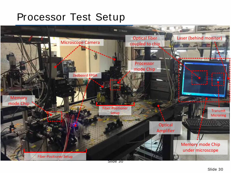
Processor Test Setup
Memory mode Chip
Processor mode Chip
Optical Amplifier
Memory mode Chip under microscope
Fiber-Positioner Setup
Fiber-Positioner Setup
Zedboard FPGA
Laser (behind monitor)Optical fiber coupled to chip
Transmit Microring
Microscope Camera
Slide 30
Slide 30
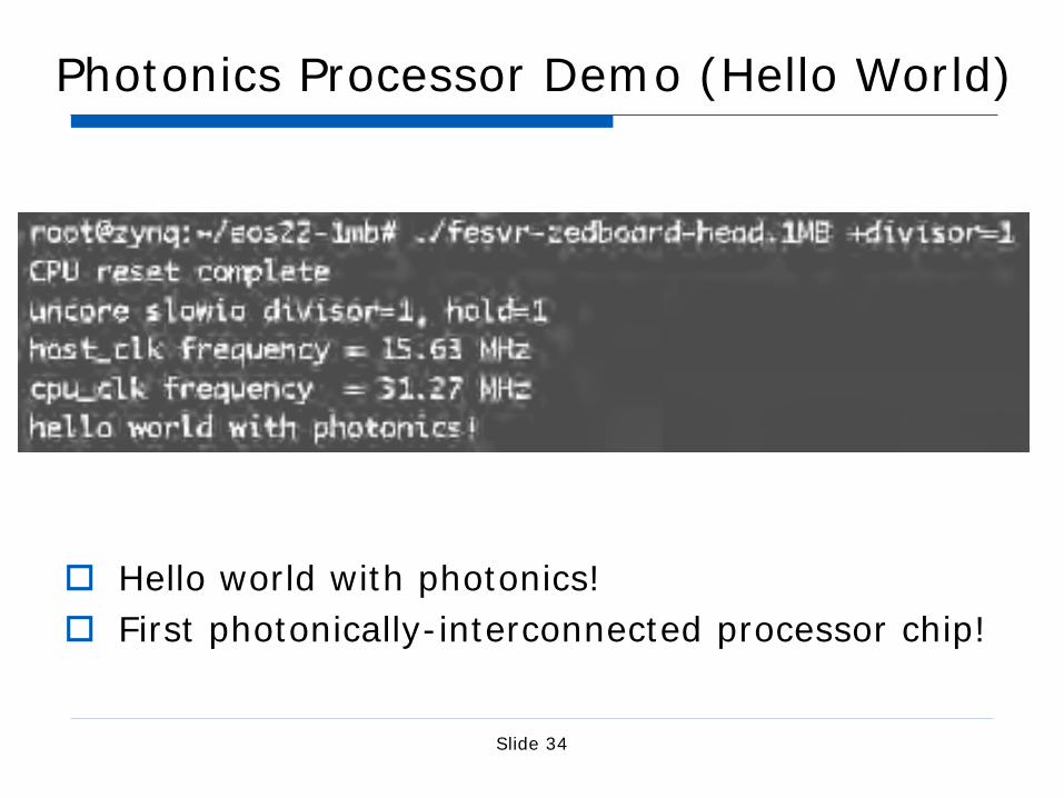
Photonics Processor Demo (Hello World)
Hello world with photonics!
First photonically-interconnected processor chip!
Slide 34

Photonics Processor Demo (STREAM)
Memory to Processor Link
Processor to Memory Link Slide 35
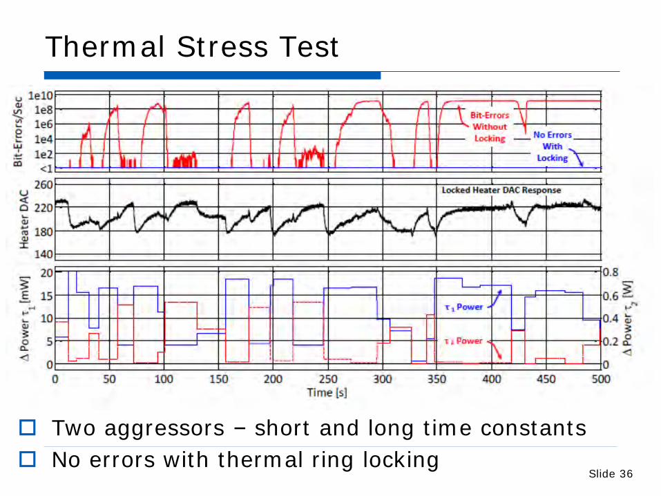
Thermal Stress Test
Two aggressors – short and long time constants
No errors with thermal ring lockingSlide 36

Platform Performance Symmary
Metric [Beamer ISCA 2010]Conservative Estimates
45nm SOI Platform
Bulk Photonics Platform*
Waveguide Loss 4 dB/cm 3.7 dB/cm 10.5 dB/cm
Vertical Coupler Loss 1 dB 1 dB 3 dB
Tx Data Rate 10 Gb/s 8 Gb/s 5 Gb/s
Tx Energy Per Bit 120 fJ/b 30 fJ/b 350 fJ/b
Rx Data Rate 10 Gb/s 10 Gb/s 5 Gb/s
Rx Energy Per Bit 80 fJ/b 297 fJ/b 1700 fJ/b
Rx Sensitivity 10 μA 8.3 μA 36 μA
PD Responsivity 0.9 A/W 0.1 A/W 0.2 A/W
Thermal Tuning Efficiency 1.6 μW/GHz 3.8 μW/GHz 10 μW/GHz
*considerably slower process than one assumed in [Beamer ISCA 2010]
• Comparison to a proposal for the processor-memory system we published 5 years ago
• Meeting/exceeding most system specsSlide 37

Monolithic Platform Summary
Demonstrated world’s first photonically connected processor chip
Demonstrated world’s first photonic link in a bulk CMOS process
Bulk and SOI photonic platforms are ready
Zero-change SOI photonics in commercial foundry
Bulk platform ready for porting to advanced process nodes
Slide 38

DRAM: Bulk photonics integration
DTI adjacent to STI
Meade et al. VLSI14, OIC13
Deep Trench Structure
Deep Trench
STI STISTI
Backend Dielectrics
Bulk Si
Poly Waveguide
FET
1.2μm
Slide 40

Process development platform
DTI adjacent to STI Micron Reticle
Independent
Photonics
Structures
Independent
Photonics
Structures
Independent
Photonics
Structures
4x
Integrated
Photonics-
Electronic
Mini-chips
24
mm
24 mm
Meade et al. VLSI14, OIC13
Slide 41
Full-reticle- Photonic device sites- Electronic-photonic
templates

Modulator in bulk process
100ps FO4 delay
Modulator Device
VREF
INO
INE
CK
VDD
Modulator Driver
Case 2Case 1VDD
VREF
ExtinctionInsertion Loss
2.5V2.1V
7.67dB1.63dB
2.0V1.5V
6.79dB2.15dB
Case 1
Case 2
5 Gb/s Tx Eye
(Case 2)
7.6dB
1.22 pJ/bit
Modulator Device
VREF
INO
INE
CK
VDD
Modulator Driver
Case 2Case 1VDD
VREF
ExtinctionInsertion Loss
2.5V2.1V
7.67dB1.63dB
2.0V1.5V
6.79dB2.15dB
Case 1
Case 2
5 Gb/s Tx Eye
(Case 2)
7.6dB
1.22 pJ/bit
42
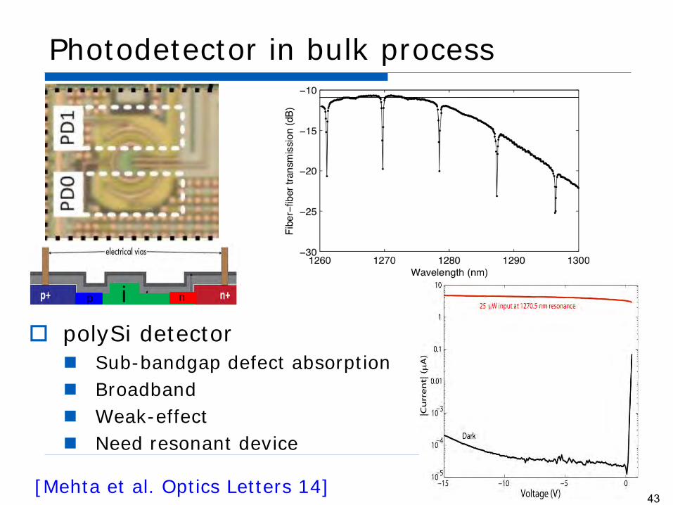
polySi detector
Sub-bandgap defect absorption
Broadband
Weak-effect
Need resonant device
Photodetector in bulk process
30[Mehta et al. Optics Letters 14]
ip n
43

Photodetector performance
20% responsivity
Further improvements with optimized cavity design
Bias-dependent bandwidth >1GHz44

Receiver in bulk process
45

Chip-to-Chip Link
Tx Macro
Modulator Driver
Receiver
Hea
ter
Dri
ver
8:2 Ser. 2:8 Des.
BER Checker
Tuning PRBS
Generator
Output Coupler
Modulator Driver
Receiver
Hea
ter
Dri
ver
8:2 Ser. 2:8 Des.
BER Checker
Tuning PRBS
Generator
Vertical Coupler
Microring Detector
Dummy Detector
Tx Macro
Vertical Coupler
Microring Modulator
Tx Macro
l1 Laserl1
Chip
100 μm 100 μm
Single-Mode Fiber
Single-Mode Fiber
Rx Macro
l1
Chip
Rx Macro
Rx Macro
46
5Gb/s, 2.8 pJ/bit circuits, 5pJ/b optical
Sun et al, VLSI14, JSSC15

WDM in bulk-photonics - Tx
All slices BER checked at 5Gb/s
45Gb/s per fiber
47
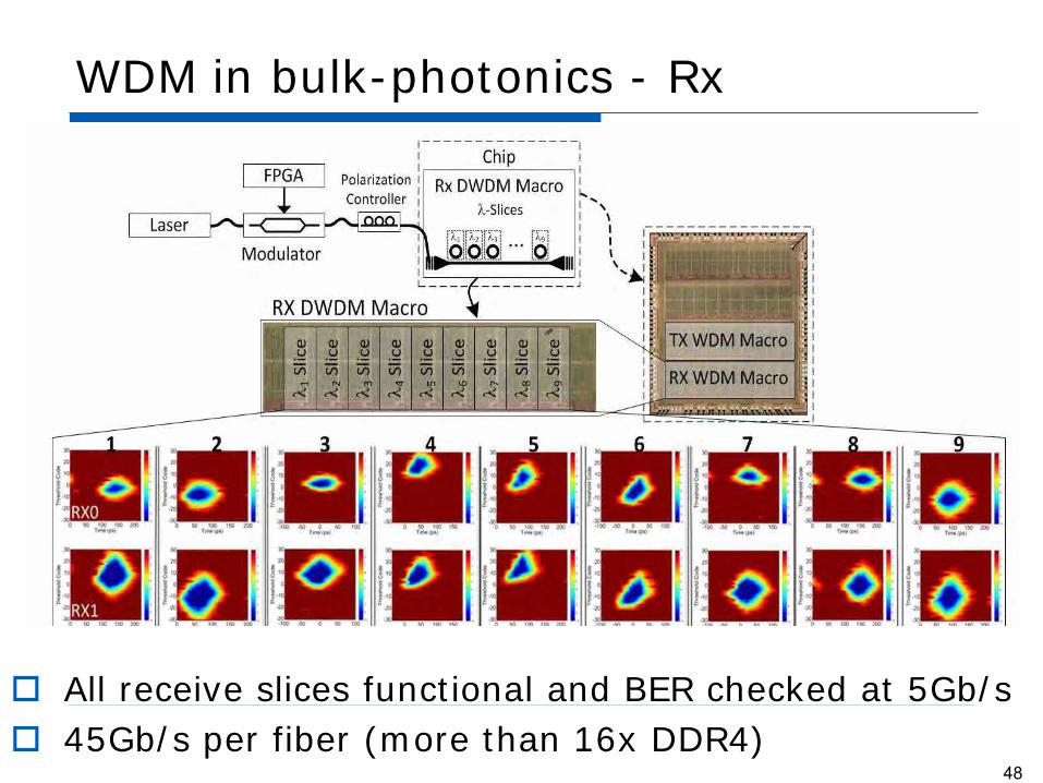
WDM in bulk-photonics - Rx
All receive slices functional and BER checked at 5Gb/s
45Gb/s per fiber (more than 16x DDR4)48