electronic band structures and phase transitions of
TRANSCRIPT

Chapter 6
Electronic Band Structures and Phase Transitions of
Ferroelectric and Multiferroic Oxides
Zhigao Hu, Junhao Chu, Yawei Li, Kai Jiang andZiqiang Zhu
Additional information is available at the end of the chapter
http://dx.doi.org/10.5772/52189
Provisional chapter
Electronic Band Structures and Phase Transitions of
Ferroelectric and Multiferroic Oxides
Zhigao Hu, Junhao Chu,
Yawei Li, Kai Jiang and Ziqiang Zhu
Additional information is available at the end of the chapter
1. Introduction
Perovskite ferroelectric (FE) materials have attracted considerable attention for a wide rangeof applications, such as dynamic random access memories (DRAM), microwave tunablephase shifters and second harmonic generators (SHGs). [1–3] Moreover, materials thathave coupled electric, magnetic, and structural order parameters that result in simultaneousferroelectricity, ferromagnetism, and ferroelasticity are known as multiferroics. [4–6] Thesemultiferroics materials have attracted a lot of attention in recent years because they canpotentially offer a whole range of new applications, including nonvolatile ferroelectricmemories, novel multiple state memories, and devices based on magnetoeletric effects.Although there are some reports on the electrical and magnetic properties of perovskite-typeferroelectric and multiferroics materials, optical properties and electronic transitions have notbeen well investigated up to now. On the other hand, phase transition is one of the importantcharacteristics for the ferroelectric/multiferroics system. As we know, the phase transition isstrongly related to the structural variation, which certainly can result in the electronic bandmodifications. Therefore, one can study the phase transition of the above material systemsby the corresponding spectral response behavior at different temperatures.
Among these materials, barium strontium titanate (BST) has been considered to be one ofthe most promising candidates for devices due to its excellent dielectric properties of highdielectric functions, low leakage current and an adjustable Curie temperature Tc throughvariation of the composition between barium titanate (BT) and strontium titanate (ST).However, the limited figure of merit at high frequency microwave region restricts the BSTpractical applications. In order to improve the physical properties of the BST materials,introducing small compositions of dopants has been used for several decades. Manyexperimental and theoretical studies have been performed on the dielectric properties ofBST in the ferroelectric state by adding dopants such as Magnesium [7, 8], Aluminum [9],Manganese (Mn) [10–12], Samarium [13], and different rare earth [14], In particular, the Mn
©2012 Hu et al., licensee InTech. This is an open access chapter distributed under the terms of the CreativeCommons Attribution License (http://creativecommons.org/licenses/by/3.0), which permits unrestricted use,distribution, and reproduction in any medium, provided the original work is properly cited.© 2013 Hu et al.; licensee InTech. This is an open access article distributed under the terms of the CreativeCommons Attribution License (http://creativecommons.org/licenses/by/3.0), which permits unrestricted use,distribution, and reproduction in any medium, provided the original work is properly cited.
2 Advances in Ferroelectrics
doping BST shows some advantages in reducing the dielectric loss, enhancing the resistivity,and increasing dielectric tunability. It can significantly improve the dielectric properties,which makes it a potential candidate for microwave elements. For example, the Mn dopingcan cause the variation of the oxygen vacancy, which is the crucial role in modifying thedielectric loss mechanism. On the other hand, the doping of Mn can also reduce the dielectricconstant peak and broaden the dielectric phase transition temperature range, which resultsin a smaller temperature coefficient of capacitance in BSMT materials. [10] Therefore, it isimportant to further investigate the physical properties of BSMT materials in order to developthe potential applications.
Meanwhile, many research groups have focused on the doping effect on the fabrications anddielectric properties for strontium barium niobate SrBi2Nb2O9 (SBN) materials. [15–20] Thesubstitution of Ca ions in the Sr site for the SBN ceramic induced the TC increasing, which isuseful for the application in high-temperature resonators. [15, 18] However, the substitution
of some rare earth ions such as La3+ or Pr3+ for Bi3+ in the Bi2O2 layers can result in a shiftfor the TC to lower temperature. [16, 20, 21] It is found that the behavior of the Nd-dopedSBN ceramic tends to change from a normal ferroelectrics to a relaxor type ferroelectricsowing to the introduction of Nd ions in the Bi2O2 layers. [16, 17, 20, 22] Up to now, adetailed understanding of the lattice dynamic properties and the phase transition behaviorof Nd-doped SBN ceramics are still lacking. Raman spectroscopy is a sensitive techniquefor investigating the structure modifications and lattice vibration modes, which can givethe information on the changes of lattice vibrations and the occupying positions of dopingions. Thus, it is a powerful tool for the detection of phase transition in the doping-relatedferroelectric materials. [22, 23]
The optical properties such as the dielectric functions provide an important insight ondielectric and ferroelectric behaviors of the material and play an important role in design,optimization, and evaluation of optoelectronic devices. [24–27] In addition, the doping ofMn or Nd can induce more defects in the lattice structure, which can affect its electronicband structures and optoelectronic properties. Hence, the doping composition dependenceof optical properties for BST and SBN ceramics is technically important for practicaloptoelectronic device development. Compared to film structure, the optical properties ofbulk material (single crystals and dense ceramics) are not affected by interface layer, stressfrom clamping by the substrate, non-stoichiometry and lattice mismatch between film andsubstrate. Hence, it is desirable to carry out a delicate investigation regarding the opticalproperties of the BSMT and SBNN ceramics. Note that spectroscopic ellipsometry (SE),Raman scattering, and transmittance spectra are potentially valuable techniques for thestudies of ferroelectric materials due to their high sensitivity of local structure and symmetry.Compared with the other techniques, they can provide dielectric functions of the materials.SE and transmittance spectra can provide optical band gap and optical conductivity, whereasRaman spectra can provide Raman-active modes of the materials. [28–31]
On the other hand, bismuth ferrite (BiFeO3, BFO) is known to be the only perovskite materialthat exhibits multiferroic at room temperature (RT). At RT, it is a rhombohedrally distortedferroelectric perovskite with the space group R3c and a Curie temperature (TC) of about 1100K. [32–36] Since the physical properties of BFO films are related to their domain structure andphase states, which is sensitive to the applied stress, composition, and fabrication conditionfor BFO materials. PLD technique has the ability to exceed the solubility of magneticimpurity and to permit high quality film grown at low substrate temperature. Recent studiesof photoconductivity, [35] photovoltaic effect, [37] and low open circuit voltage in a workingsolar device, [38] illustrate the potential of polar oxides as the active photovoltaic material.
Advances in Ferroelectrics110

Electronic Band Structures and Phase Transitions of Ferroelectric and Multiferroic Oxides 3
In spite of the promising properties, there are no systematical reports focused on the opticalproperties of BFO films. In order to make BFO useful in actual electrical and optoelectronicdevices, the physical properties, especially for electronic band structure and optical responsebehavior, need to be further clarified.
The objectives of the chapter will tentatively answer the interesting questions: (1) Is therean effective method to directly analyze electronic structure of FE materials by opticalspectroscopy? (2) What kind of temperature dependence have FE oxides from band-to-bandtransitions? (3) Can spectral response at high-temperature be used to judge phase transition?Correspondingly, this chapter is arranged in the following way. In Sec. 2, detailed growthsof Ba0.4Sr0.6−xMnxTiO3 (BSMT), SrBi2−xNdxNb2O9 (SBNN) ceramics and BFO films aredescribed; In Sec. 3, solid state spectroscopic techniques are introduced; In Sec. 4, electronicband structures of BSMT ceramics are presented; In Sec. 5, phase transitions of SBNNceramics are derived; In Sec. 6, temperature effects on electronic transitions of BFO filmshave been discussed; In Sec. 7, the main results and remarks are summarized.
2. Experimental
2.1. Fabrications of FE ceramics
The ceramics based on Ba0.4Sr0.6−xMnxTiO3 (with x = 1, 2, 5 and 10%) specimens wereprepared by the conventional solid-state reaction sintering. High purity BaCO3 (99.8%),SrCO3 (99.0%), TiO2 (99.9%), and MnCO3 were used as the starting materials. Weightedpowers were mixed by ball milling with zirconia media in the ethanol as a solvent for 24 hand then dried at 110 ◦C for 12 h. After drying, the powders were calcined at 1200 ◦C for 4h, and then remilled for 24 h to reduce the particle size for sintering. The calcined powderswere added with 8 wt.% polyvinyl alcohol (PVA) as a binder. The granulated powders werepressed into discs in diameter of 10 mm and thickness of 1.0 mm. The green pellets werekept at 550 ◦C for 6 h to remove the solvent and binder, followed by sintering at 1400 ◦C for4 h. More details of the preparation process can be found in Ref. [39]. On the other hand,the SBNN (x=0, 0.05, 0.1, and 0.2) ceramics were prepared by a similar method, and SrCO3,Bi2O3, Nb2O5, and Nd2O3 were used as the starting materials. Details of the fabricationprocess for the ceramics can be found elsewhere. [17, 40]
2.2. Depositions of BFO films
The BiFeO3 films were deposited on c-sapphire substrates by the PLD technique. The BiFeO3
targets with a diameter of 3 cm were prepared through a conventional solid state reactionmethod using reagent-grade Bi2O3 (99.9%) and Fe2O3 (99.9%) powders. Weighed powderswere mixed for 24 h by ball milling with zirconia media in ethanol and then dried at 100 ◦Cfor 12 h. The dried powders were calcined at about 680 ◦C in air for 6 h to form the desiredphase, and followed by sintering at about 830 ◦C for 2 h. Before the deposition of the BFOfilms, c-sapphire substrates need to be cleaned in pure ethanol with an ultrasonic bath toremove physisorbed organic molecules from the surfaces, followed by rinsing several timeswith de-ionized water. Then the substrates were dried in a pure nitrogen stream before thefilm deposition. A pulsed Nd:YAG (yttrium aluminum garnet) laser (532 nm wavelength,5 ns duration) operated with an energy of 60 mJ/pulse and repetition rate of 10 Hz wasused as the ablation source. The films were deposited immediately after the target was
Electronic Band Structures and Phase Transitions of Ferroelectric and Multiferroic Oxideshttp://dx.doi.org/10.5772/52189
111

4 Advances in Ferroelectrics
20 30 40 50 60 70 80
Inte
nsity
(arb
.uni
t)
2 (Deg.)(1
10)
(100
) (111
)
(200
)
(210
) (211
)
(220
)(3
00)
(310
)
1%
2%
5%
10%
Ba0.4Sr0.6-xMn
Figure 1. The XRD patterns of the BSMT ceramics with the Mn composition of 1, 2, 5 and 10%, respectively.
preablated in order to remove any surface contaminants. The distance between the targetand the substrate was kept at 3 cm. The deposition time was set to about 30 min. Finally,the films were annealed at 600 ◦C in air atmosphere by a rapid thermal annealing process. Adetailed preparation of the films can be found in Ref. [6].
3. Optical spectroscopy
The ellipsometric measurements were carried out in the photon energy range of 0.7-4.2 eV(300-1700 nm) with a spectral resolution of 5 nm by near-infrared-ultraviolet (NIR-UV) SE(SC630UVN by Shanghai Sanco Instrument, Co., Ltd.). The measurements were performedunder the incident angle of 67◦ for all the ceramics corresponding to the experimentaloptimization near the Brewster angle of the BSMT. Raman scattering experiments werecarried out using a Jobin-Yvon LabRAM HR 800 UV micro-Raman spectrometer, excitedby a 632.8 nm He-Ne laser with a spectral resolution of 0.5 cm−1. Temperature dependentmeasurements from 80 to 873 K were performed using the Linkam THMSE 600 heating stage,and the set-point stability is of better than 0.5 K. The normal-incident transmittance spectrawere recorded using a double beam ultraviolet-infrared spectrophotometer (PerkinElmerLambda 950) at the photon energy from 0.5 to 6.5 eV (190-2650 nm) with a spectral resolutionof 2 nm. The samples at 5.3-300 K were mounted into an optical cryostat (Janis SHI-4-1) forvariable temperature experiments. [41]
4. Electronic band structures of BSMT ceramics
The XRD patterns of the BSMT ceramics with different Mn composition are shown in Fig. 1and no secondary phase appears within the detection limit of the XRD. Besides the strongest(110) peak, some weaker peaks (100), (111), (200), (210), (211), (220) can be also observed,which indicate that the ceramics are polycrystalline with single perovskite phase. Thediffraction patterns are fitted by the Gaussian lineshape analysis to extract the peak positionsand full width at half maximum (FWHM). The lattice constant a of the BSMT ceramics,which can be estimated from the (110) diffraction peak, is calculated to be about 3.954 Å. [39]The ionic radius of Mn2+ (1.27 Å) is smaller than that of Sr2+ (1.44 Å) and Ba2+ (1.61 Å),and is larger than that of Ti4+ (0.61 Å), which can be attributed to the change of the latticeconstant. When the Mn composition is below 5%, the (110) diffraction peak positions shiftfrom smaller angles to larger angles and the lattice constant slightly decreases, which can be
Advances in Ferroelectrics112
Electronic Band Structures and Phase Transitions of Ferroelectric and Multiferroic Oxides 5
6
12
18 1% 2% 5% 10%
(Deg
.)
(a)
1 2 3 440
80
120 (D
eg.)
Figure 2. Experimental ellipsometric data (a) Ψ and (b) ∆ for the BSMT ceramics from near-infrared to ultraviolet photon energy
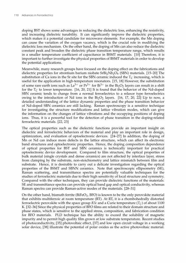
region at the incident angle of 67◦. (Figure reproduced with permission from [39]. Copyright 2012, Springer.)
4
6
8
1
(a)
1 2 3 4
2
4
6
2
Photon energy (eV)
(b)
1% 2%
Figure 3. The (a) real and (b) imaginary parts of the NIR-UV dielectric functions for the BSMT ceramics with different Mn
composition. (Figure reproduced with permission from [39]. Copyright 2012, Springer.)
ascribed to the fact that Mn occupies the A site together with Ba2+ and Sr2+. In order toreduce distortion of the crystal lattice, the Mn mainly substitutes Sr2+ because the differencesin ionic radius between Mn ion and Ba ion is larger than that between Mn and Sr. On theother hand, when the Mn composition is larger than 5%, the excess Mn can also substitutethe Ti site, which results in the increase of the lattice constant and the smaller shift of thepeak position. It can be concluded that the Mn ions substitute Sr sites of the BST lattice atfirst, then occupy Ti sites when the Mn composition is beyond 5%.
The experimental ellipsometric spectra of Ψ and ∆ recorded at an incident angle of 67◦ forthe BSMT ceramics are depicted in Figs. 2(a) and (b), respectively. The observed changesin the Ψ and ∆ data for different Mn composition may be attributed to the lattice distortionand variation in atomic coordinate. Because the sample is bulk material with a thickness ofseveral millimeters, the dielectric functions of the BSMT ceramics can be directly calculated
Electronic Band Structures and Phase Transitions of Ferroelectric and Multiferroic Oxideshttp://dx.doi.org/10.5772/52189
113

6 Advances in Ferroelectrics
2.0 2.5 3.0 3.5 4.00
2
4
1% 2%
5% 10%
(E)
2 /(x1
012eV
2 cm
-2)
Photon energy (eV)
(eV)0 5 10
3.45
3.60
Mn Composition (%)
Figure 4. Absorption coefficient vs. incident photon energy near the optical band gap of the BSMT ceramics. The insert isthe optical band gap Eg with the different Mn composition. (Figure reproduced with permission from [39]. Copyright 2012,
Springer.)
according to the ellipsometric spectra Figs. 3(a) and (b) show the real (ε1) and imaginary (ε2)parts of the dielectric functions in the photon energy range of 0.7-4.2 eV, respectively. Theevolution of ε with the photon energy is a typical optical response behavior of ferroelectricand/or semiconductors. The optical band gap (Eg) of the BSMT ceramics is one of theimportant optical behaviors, which is calculated by considering a direct transition from theVB to the CB when the photon energy falls on the materials. In the BSMT system, theVB is mainly composed of the O 2p orbital and the CB is mainly composed of the Ti 3dorbital. It should be noted that because of the splitting of the Ti 3d conduction bands intot2g and eg subbands, the lowest CB arises from the threefold degenerate Ti 3d t2g orbital,which has lower energy than the twofold degenerate Ti 3d eg orbital. [42] The absorptioncoefficient related Eg of the BSMT ceramics can be determined according to the Tauc’s law:
(αE)2 = A(E− Eg), where A is a constant, α and E are the absorption coefficient and incident
photon energy, respectively. For the allowed direct transition, the straight line between (αE)2
and E will provide the value of the band gap, which is extrapolated by the linear portionof the plot to (αE)2=0, as seen in Fig. 4. The Eg is estimated to 3.65, 3.57, 3.40 and 3.60 eVcorresponding to x=1, 2, 5 and 10% for the BSMT ceramics, respectively, as shown in theinset of Fig. 4. The results suggest that the band gap of the BSMT ceramics decreases andthen increases with increasing Mn composition.
As we know, the optical band gap can be affected by some factors such as grain size, oxygenvacancy, stress and amorphous nature of the materials. [2] The decreasing trend of theband gap with the Mn composition below 5% can be attributed to the increase of the grainsize and the smaller lattice constant, which are caused by the Mn introduction in the Asites. When the Mn composition is 10%, there is a sharp increase in the optical band gapbecause the excess Mn will substitute the Ti site at the Mn composition of 10%, causing theincrease of the oxygen vacancies. In addition, the creation of an oxygen vacancy which isassociated with the generation of free charge carriers can be described as the following:
MnO(−TiO2) → Mn′′
Ti + V··
O + OO; OO → V··
O + 2e− + 1/2O2, where V··
O represents thedoubly charged oxygen vacancy, OO is an oxygen ion at its normal site, e− is the freeelectronic charge generated through the vacancy formation. [9, 43] The heavy doping blocksthe lowest states in the CB and the effective band-gap increases, which is known as theBurstein-Moss (BM) effect. [44] When a large number of vacancy-related charge carriers are
Advances in Ferroelectrics114

Electronic Band Structures and Phase Transitions of Ferroelectric and Multiferroic Oxides 7
200 400 600 800
x=0.2x=0.1x=0.05
Inte
nsity
(arb
. uni
ts)
Raman shift (cm-1)
61
97
179
207
281310 456 579
835
x=0
(a)
435
0.0 0.1 0.2200
210
Nd composition
834
840
A1g[Nb]
A1g[O](b)
Figure 5. Raman scattering spectra of the SBNN ceramics with different Nd composition (x) recorded at RT. The dashed linesclearly indicate some Raman-active phonon modes. The inset shows the peak frequency variation of the A1g [Nb] phonon modeat about 207 cm−1 and the A1g [O] phonon mode at about 836 cm−1 as a function of Nd composition. (Figure reproduced with
permission from [46]. Copyright 2012, Wiley.)
generated in the system, the lowest lying states in the CB are filled and the vertical distanceneeded for the optical transition increases. [44] Hence, it can be concluded that, when the Mncomposition is 10%, the sharply increase in the band gap may be attributed to the BM shiftcaused by electrons generated by oxygen vacancies. Besides, the grain size for the ceramicdecreases induced by the heavy doping with the Mn composition of 10%, which may alsoresult in a sharply increase of the optical band gap. It can be concluded that the differenceof the optical band gap could be due to the dopant composition, the oxygen vacancies, andthe crystallinity of the BSMT ceramics.
5. Phase transitions of SBNN ceramics
The general formula of bismuth layer structure ferroelectrics (BLSFs) is given as (Bi2O2)2+
(Am−1BmO3m+1)2−, where A and B are the two types of cations that enter the perovskite
unit, and m is the the number of perovskite unit cell between bismuth oxide layers. [20]SBN, which is known to be m=2 member of BLSFs family, has been regarded as a promisingferroelectric material due to low dielectric constants and excellent fatigue resistance. [40] Fig.5(a) shows the Raman spectra of the SBNN ceramics with different Nd compositions at RTin the spectral range of 50 − 950 cm−1. The Raman selection rules allow 18 phonon modes(4A1g + 2B1g + 6B2g + 6B3g) for SBN ceramics at RT. [45] However, less than 10 phononmodes are observed because of the possible overlap of the same symmetry vibration or theweak feature of some vibration bands. [46, 47] According to the assignment of SrBi2Nb2O9
single crystal, [45] the Raman phonon modes at about 61, 207 and 835 cm−1 can be assignedto the A1g phonon mode, the vibrations at about 179 and 579 cm−1 can be assigned to the Eg
phonon mode. However, the assignment of other phonon modes are still not clear now. Theinternal vibrations of NbO6 octahedra occur in the high-frequency mode region above 200cm−1 because the intragroup binding energy within the NbO6 octahedra is much larger thanthe intergroup or crystal binding energy. [15] The composition dependence of the frequenciesfor two typical phonon modes is illustrated in Fig. 5(b). Note that the A1g[Nb] phonon mode
at 207 cm−1, which arises from the distortion of NbO6 octahedra, generally decreases withthe Nd composition, whereas the A1g[O] phonon mode at 835 cm−1 mode corresponding tothe symmetric Nb−O stretching vibration, increases with the introduction of Nd ions.
Electronic Band Structures and Phase Transitions of Ferroelectric and Multiferroic Oxideshttp://dx.doi.org/10.5772/52189
115

8 Advances in Ferroelectrics
100 200 300
**(c)
Raman shift (cm-1)
x=0.2
80-873 K
600 900
## (d)
A1g[O]
100 200 300
*
A1g[Nb]x=0
Inte
nsity
(arb
.uni
ts)
(a)
A 1g[B
i]Eg[Nb]
*
600 900
# (b)
873 K
80 K
A1g[O]#
Figure 6. Temperature dependence of the SBNN ceramics with the composition of (a)(b) x=0 and (c)(d) x=0.2. The solid arrowsindicate the temperature increasing from 80 K to 873 K, and the dash arrows show the shift of the frequency for the phononmodes with the temperature. The symbol asterisk (∗) and pound sign (#) indicate the two weak Eg phonon modes in the range
of 281-310 cm−1 and 435-456 cm−1, respectively. (Figure reproduced with permission from [46]. Copyright 2012, Wiley.)
In order to further understand the effect of Nd3+ ion substitution on the phonon modes, Fig.6 presents the temperature dependence of the Raman spectra for the SBNN ceramics withtwo Nd compositions of x=0 and 0.2 in the temperature range from 80 to 873 K. It suggeststhat the intensities for all the phonon modes increase with the temperature except for thephonon mode at about 579 cm−1, whose peak has been overwhelmed at high temperature.The broadening band can be assigned to a rigid sublattice mode, in which all the positive andnegative ion displacements are equal and opposite. [48] It is found that a strong broadeningpeak can be observed at 80 K due to the combined effects of two modes splitting from the Eg
character mode. However, with increasing the temperature, the frequency and intensity ofthe mode present a decreasing trend. Because the mode is assigned to the asymmetric Nb−Ovibration, it can be concluded that the NbO6 octahedra is sensitive to the temperature. On theother band, the phonon modes at about 281 and 310 cm−1 (labeled by ∗), which are associatedwith the O−Nb−O bending, become more difficult to be distinguished as the temperatureincreases and disappear at high temperature. Similar phenomena can be observed for thephonon modes in the range of 435-456 cm−1 (labeled by #). The band at about 456 cm−1,which is described to a Ti−O torsional mode, has been assigned as the Eg character and splits
into two phonon modes centered at 435 and 456 cm−1 at lower temperature. As pointed outby Graves et al., [45] it can be ascribed to the fact that the several Eg phonon modes split intothe B2g and B3g phonon modes during the tetragonal to orthorhombic transition. Moreover,the splitting of the phonon modes reveals the structural changes in the SBNN ceramics withthe temperature.
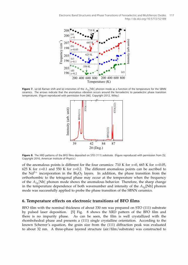
Considering that the phase transition temperature is related to the distortion extent of theNbO6 octahedra for the SBNN ceramics, the temperature dependence of the Raman shiftfor the A1g[Nb] phonon mode is plotted in Fig. 7(a)-(d). For all the SBNN ceramics, thedecrease of the A1g[Nb] phonon mode can be observed as the temperature is increased. Notethat an obviously anomalous vibration occurs around the phase transition temperatures: theRaman shift sharply increases with increasing the temperature. In addition, the temperature
Advances in Ferroelectrics116
Electronic Band Structures and Phase Transitions of Ferroelectric and Multiferroic Oxides 9
200208
710 K
x=0(a)
198207
(b)
Freq
uenc
y (c
m-1)
665 K
x=0.05
196203
(c)
625 K
x=0.1
200 400 600 800196203
(d)
Temperature (K)
550 K
x=0.2200 400 600 800
(e)
Inte
nsity
(arb
.uni
ts)
Figure 7. (a)-(d) Raman shift and (e) intensities of the A1g [Nb] phonon mode as a function of the temperature for the SBNNceramics. The arrows indicate that the anomalous vibration occurs around the ferroelectric to paraelectric phase transition
temperatures. (Figure reproduced with permission from [46]. Copyright 2012, Wiley.)
39 42 84 87
STO
(222
)
BFO
(222
)
STO
(111
)
Inte
nsity
(arb
. uni
t)
2 (Deg.)
BFO
(111
)
Figure 8. The XRD patterns of the BFO films deposited on STO (111) substrate. (Figure reproduced with permission from [5].
Copyright 2010, American Institute of Physics.)
of the anomalous points is different for the four ceramics: 710 K for x=0, 665 K for x=0.05,625 K for x=0.1 and 550 K for x=0.2. The different anomalous points can be ascribed tothe Nd3+ incorporation in the Bi2O2 layers. In addition, the phase transition from theorthorhombic to the tetragonal phase may occur at the temperature when the frequencyof the A1g[Nb] phonon mode shows the anomalous behavior. Therefore, the sharp changein the temperature dependence of both wavenumber and intensity of the A1g[Nb] phononmode was successfully applied to probe the phase transition of the SBNN ceramics.
6. Temperature effects on electronic transitions of BFO films
BFO film with the nominal thickness of about 330 nm was prepared on STO (111) substrateby pulsed laser deposition. [5] Fig. 8 shows the XRD pattern of the BFO film andthere is no impurity phase. As can be seen, the film is well crystallized with therhombohedral phase and presents a (111) single crystalline orientation. According to theknown Scherrer’s equation, the grain size from the (111) diffraction peak was evaluatedto about 32 nm. A three-phase layered structure (air/film/substrate) was constructed to
Electronic Band Structures and Phase Transitions of Ferroelectric and Multiferroic Oxideshttp://dx.doi.org/10.5772/52189
117

10 Advances in Ferroelectrics
2.4 2.80.0
0.3
0.65.3 K
150 K
Tran
smittan
ce
Photon energy (eV)
300 K
BiFeO3
1 2 3 4 5 60.0
0.4
0.8
Photon energy (eV)
+0.2
Figure 9. Experimental (dotted curves) and fitting (solid curves) transmittance spectra at temperatures of 300 and 5.3 K,
respectively. The inset shows the enlarged band gap region of the BFO film at temperatures of 300, 200, and 5.3 K, respectively.
(Figure reproduced with permission from [5]. Copyright 2010, American Institute of Physics.)
simulate the transmittance spectra of the BFO film. It should be emphasized that thenormal-incident transmittance spectra cannot be sensitive to the thinner surface rough layer,which could be several nanometers and much less than the film thickness. Therefore,the surface rough layer can be reasonably neglected owing to a slight contribution in theevaluation of the optical properties. The optical constants of the BFO film can be expressedusing four Tauc-Lorentz (TL) oscillators. [50] As an example, the experimental and fittingtransmittance spectra of the BFO film at 300 and 5.3 K are shown in Fig. 9 with the dottedand solid curves, respectively. Note that the symmetrical interference period indicates thatthe film is of good uniformity and crystallization. From Fig. 9, it can be observed that theabsorption edge remarkably shift toward the lower energy with increasing the temperature,suggesting that the OBG of the film has a negative temperature coefficient. Note thatthe shift at high temperature region (100-300 K) is larger than that at low temperatureregion (5.3-100 K). This is because the quantities of the conduction band downward andthe valence band upward are different under the distinct temperature regions. Especially,two broadening shoulder structures appear and the intensities become much stronger withdecreasing the temperature. The similar phenomena have been observed at 2.5 eV when thetemperature decreases to about 4 K, which represents the onset of the optical absorption.[51] Furthermore, the shoulders are simply low-lying features of the electronic structure orevidence for excitonic character.
Based on the theoretical calculations and experimental observations, the four energy bandscan be uniquely assigned to the following electronic transitions: (1) on-site Fe3+ d to dcrystal field transition; (2) majority channel Fe 3d to O 2p charge transfer excitation; (3)minority channel dipole-allowed O p to Fe d charge transfer excitation; and (4) stronghybridized majority channel O p and Fe d to Bi p state excitation, respectively. [51–55]Within the experimental error bars, the energy positions shift toward the higher energy at thetemperature of 5.3 K except for the second excitation, which can be attributed to the energyband variations. Nevertheless, the origin of the abnormal shift for the second excitation isunclear in the present work. Under the influence of the tetrahedral crystal field, the Fe 3dorbital states split into t2g and eg state and the t2g state strongly hybrided with the O p orbital.[52] With decreasing the temperature, the t2g and eg states can be located at different level in
Advances in Ferroelectrics118
Electronic Band Structures and Phase Transitions of Ferroelectric and Multiferroic Oxides 11
-10
0
10
20 5.3 K 200 K 300 K
1
1 2 3 4 5 60
10
20
30
0 100 200 300
2.66
2.68
2.70
(eV)
Temperature (K)
BiFeO3/SrTiO3
Eg
Figure 10. The dielectric functions of the BFO films in the photon energy range of 0.5-6.5 eV at 300, 200, and 5.3 K,
respectively. The inset shows the temperature dependence of the Eg (dotted curve) and Bose-Einstein model fitting result (solid
curve). (Figure reproduced with permission from [5]. Copyright 2010, American Institute of Physics.)
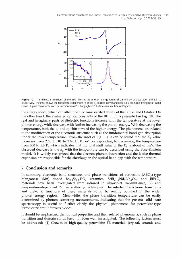
the energy space, which can affect the electronic excited ability of the Bi, Fe, and O states. Onthe other hand, the evaluated optical constants of the BFO film is presented in Fig. 10. Thereal and imaginary parts of dielectric functions increase with the temperature at the lowerphoton energy while decrease with further increasing the photon energy. With decreasing thetemperature, both the ε1 and ε2 shift toward the higher energy. The phenomena are relatedto the modification of the electronic structure such as the fundamental band gap absorptionunder the lower temperature. From the inset of Fig. 10, it can be found that the Eg valueincreases from 2.65 ± 0.01 to 2.69 ± 0.01 eV, corresponding to decreasing the temperaturefrom 300 to 5.3 K, which indicates that the total shift value of the Eg is about 40 meV. Theobserved decrease in the Eg with the temperature can be described using the Bose-Einsteinmodel. It is widely recognized that the electron-phonon interaction and the lattice thermalexpansion are responsible for the shrinkage in the optical band gap with the temperature.
7. Conclusion and remarks
In summary, electronic band structures and phase transitions of perovskite (ABO3)-typeManganese (Mn) doped Ba0.4Sr0.6TiO3 ceramics, SrBi2−xNdxNb2O9, and BiFeO3
materials have been investigated from infrared to ultraviolet transmittance, SE andtemperature-dependent Raman scattering techniques. The interband electronic transitionsand dielectric functions of these materials could be readily obtained in the widerphoton energy region. Meanwhile, the phase transition temperature can be easilydetermined by phonon scattering measurements, indicating that the present solid statespectroscopy is useful to further clarify the physical phenomena for perovskite-typeferroelectric/multiferroics oxides.
It should be emphasized that optical properties and their related phenomena, such as phasetransition and domain status have not been well investigated. The following factors mustbe addressed: (1) Growth of high-quality perovskite FE materials (crystal, ceramic and
Electronic Band Structures and Phase Transitions of Ferroelectric and Multiferroic Oxideshttp://dx.doi.org/10.5772/52189
119
12 Advances in Ferroelectrics
film); (2) Theoretical model and explanations; (3) Improved experimental methods. As forsolid state spectroscopic technique, however, it can uniquely discover the electronic bandstructure of FE system. One can think that the electronic transition will be changed duringthe phase transition process owing to the crystal structure variation. Thus, we can checkthe status by recording the spectral response. Evidently, some optical setup at elevatedtemperatures are necessary because most of FE materials have the high TC. In our researchgroup, Transmittane/Reflectance, SE, and Raman systems from LHe temperature to about800 K have been developed. Our next goal is to characterize the physical information of sometypical FE materials in a wider spectral and temperature ranges, which play an importantrole in clarifying the structure transitions and the intrinsic origin.
Acknowledgments
The authors would like to thank Dr. Wenwu Li for valuable discussions. This workwas financially supported by the Major State Basic Research Development Program ofChina (Grant Nos. 2011CB922200 and 2013CB922300), the Natural Science Foundationof China (Grant Nos. 11074076, 60906046 and 61106122), the Program of New CenturyExcellent Talents, MOE (Grant No. NCET-08-0192) and PCSIRT, the Projects of Science andTechnology Commission of Shanghai Municipality (Grant Nos. 11520701300, 10DJ1400201and 10SG28), and the Program for Professor of Special Appointment (Eastern Scholar) atShanghai Institutions of Higher Learning.
Author details
Zhigao Hu1,⋆, Junhao Chu1,2,⋆,Yawei Li1, Kai Jiang1 and Ziqiang Zhu1
1 Key Laboratory of Polar Materials and Devices, Ministry of Education, Department ofElectronic Engineering, East China Normal University, Shanghai, People’s Republic of China2 National Laboratory for Infrared Physics, Shanghai Institute of Technical Physics, ChineseAcademy of Sciences, Shanghai, People’s Republic of China
References
[1] Nagaraj, B.; Sawhney, T.; Perusse, S.; Aggarwal, S.; Ramesh, R.; Kaushik, V. S.; Zafar, S.;Jones, R. E.; Lee, J. -H.; Balu, V. & Lee, J. (1999). (Ba,Sr)TiO3 thin films with conductingperovskite electrodes for dynamic random access memory applications. Appl. Phys.Lett., 74, 21, 3194-3196
[2] Roy, S. C.; Sharma, G. L. & Bhatnagar, M. C. (2007). Large blue shift in the opticalband-gap of sol-gel derived Ba0.5Sr0.5TiO3 thin films. Solid State Commun., 141, 5,243-247
[3] Kozyrev, A. B.; Kanareykin, A. D.; Nenasheva, E. A.; Osadchy, V. N. & Kosmin, D. M.(2009). Observation of an anomalous correlation between permittivity and tunability ofa doped (Ba,Sr)TiO3 ferroelectric ceramic developed for microwave applications. Appl.Phys. Lett., 95, 01, 012908(1-3)
Advances in Ferroelectrics120
Electronic Band Structures and Phase Transitions of Ferroelectric and Multiferroic Oxides 13
[4] Catalan, G. & Scott, J. F. (2009). Physics and applications of bismuth ferrite. Adv. Mater.,21, 24, 2463-2485
[5] Li, W. W.; Zhu, J. J.; Wu, J. D.; Gan, J.; Hu, Z. G.; Zhu, M. & Chu, J. H. (2010).Temperature dependence of electronic transitions and optical properties in multiferroicBiFeO3 nanocrystalline film determined from transmittance spectra. Appl. Phys. Lett.,97, 12, 121102(1-3)
[6] Jiang, K.; Zhu, J. J.; Wu, J. D.; Sun, J.; Hu, Z. G. & Chu, J. H. (2011). Influences of oxygenpressure on optical properties and interband electronic transitions in multiferroicbismuth ferrite nanocrystalline films grown by pulsed laser deposition. ACS Appl.Mater. Interfaces, 03, 12, 4844-4852
[7] Su, B. & Button, T. W. (2004). Microstructure and dielectric properties of Mg-dopedbarium strontium titanate ceramics. J. Appl. Phys., 95, 03, 1382-1385
[8] Xu, S.; Qu, Y. & Zhang, C. (2009). Effect of Mg2+ content on the dielectric properties ofBa0.65−xSr0.35MgxTiO3 ceramics. J. Appl. Phys., 106, 01, 014107(1-5)
[9] Kim, S. S. & Park, C. (1999). Leakage current behaviors of acceptor- and donor-doped(Ba0.5Sr0.5)TiO3 thin films. Appl. Phys. Lett., 75, 17, 2554-2556
[10] Yuan, Z.; Lin, Y.; Weaver, J.; Chen, X.; Chen, C. L.; Subramanyam, G.; Jiang, J. C. &Meletis, E. I. (2005). Large dielectric tunability and microwave properties of Mn-doped(Ba,Sr)TiO3 thin films. Appl. Phys. Lett., 87, 15, 152901(1-3)
[11] Zhang, J. J.; Zhai, J. W. & Yao, X. (2009). Dielectric tunable properties of low-lossBa0.4Sr0.6Ti1−yMnyO3ceramics. Scripta Mater., 61, 07, 764-767
[12] Liu, M.; Ma, C.; Collins, G.; Liu, J.; Chen, C.; Shui, L.; Wang, H.; Dai, C.; Lin, Y.;He, J.; Jiang, J.; Meletis, E. I. & Zhang, Q. (2010). Microwave dielectric properties withoptimized Mn-doped Ba0.6Sr0.4TiO3 highly epitaxial thin films. Cryst. Growth Des., 10,10, 4221-4223
[13] Li, Y. L. & Qu, Y. F. (2009). Dielectric properties and substitution mechanism ofsamarium-doped Ba0.68Sr0.32TiO3 ceramics. Mater. Res. Bull., 44, 01, 82-85
[14] Zhang, J. J.; Zhai, J. W.; Chou, X. J. & Yao, X. (2008). Influence of rare-earth addition onmicrostructure and dielectric behavior of Ba0.6Sr0.4TiO3 ceramics. Mater. Chem. Phys.,111, 02, 409-413
[15] Huang, S. M.; Li, Y. C.; Feng, C. D.; Gu, M. & Liu, X. L. (2008). Dielectric and structuralproperties of layer-structured Sr1−xCaxBi2Nb2O9. J. Am. Ceram. Soc., 91, 09, 2933-2937
[16] Huang, S. M.; Feng, C. D.; Chen, L. D. & Wen, X. W. (2005). Dielectric properties ofSrBi2−xPrxNb2O9 ceramics (x=0, 0.04 and 0.2). Solid State Commun., 133, 6, 375-379
[17] Sun, L.; Feng, C. D.; Chen, L. D. & Huang, S. M. (2007). Effect of substitution ofNd3 for Bi3 on the dielectric properties and structures of SrBi2−xNdxNb2O9 bismuthlayer-structured ceramics. J. Appl. Phys., 101, 08, 084102(1-5)
Electronic Band Structures and Phase Transitions of Ferroelectric and Multiferroic Oxideshttp://dx.doi.org/10.5772/52189
121
14 Advances in Ferroelectrics
[18] Wu, Y.; Forbess, M. J.; Seraji, S.; Limmer, S. J.; Chou, T. P.; Nguyen, C. & Cao, G.(2001). Doping effect in layer structured SrBi2Nb2O9 ferroelectrics. J. Appl. Phys., 90,10, 5296-5302
[19] Liu, G. Z.; Wang, C.; Gu, H. S. & Lu, H. B. (2007). Raman scattering study of La-dopedSrBi2Nb2O9 ceramics. J. Phys. D: Appl. Phys., 40, 24, 7817-7820
[20] Fang, P.; Fan, H.; Li, J. & Liang, F. (2010). Lanthanum induced larger polarizationand dielectric relaxation in Aurivillius phase SrBi2−xLaxNb2O9 ferroelectric ceramics.J. Appl. Phys., 107, 06, 064104(1-4)
[21] Verma, M.; Sreenivas, K. & Gupta, V. (2009). Influence of La doping on structural anddielectric properties of SrBi2Nb2O9 ceramics. J. Appl. Phys., 105, 02, 024511(1-6)
[22] Speghini, A.; Bettinelli, M.; Caldino, U.; Ramírez, M. O.; Jaque, D.; Bausa, L. E. & Sole,J. G. (2006). Phase transition in SrxBa1−xNb2O6 ferroelectric crystals probed by Ramanspectroscopy. J. Phys. D: Appl. Phys., 39, 23, 4930-4934
[23] Tenne, D. A.; Bruchhausen, A.; Kimura, N. D. L.; Fainstein, A.; Katiyar, R. S.; A.Cantarero,; Soukiassian, A.; Vaithyanathan, V.; Haeni, J. H.; Tian, W.; Schlom, D. G.;Choi, K. J.; Kim, D. M.; Eom, C. B.; Sun, H. P.; Pan, X. Q.; Li, Y. L.; Chen, L. Q.; Jia, Q. X.;Nakhmanson, S. M.; Rabe, K. M. & Xi, X. X. (2006). Probing nanoscale ferroelectricityby ultraviolet Raman spectroscopy. Science, 313, 5793, 1614-1616
[24] Zhu, J. J.; Li, W. W.; Xu, G. S.; Jiang, K.; Hu, Z. G. & Chu, J. H.(2011). A phenomenalogical model of electronic band structure in ferroelectricPb(In1/2Nb1/2)O3-Pb(Mg1/3Nb2/3)O3-PbTiO3 single crystals around morphotropicphase boundary determined by temperature-dependent transmittance spectra. ActaMaterialia, 59, 17, 6684-6690
[25] Zhang, W. J.; Li, W. W.; Chen, X. G.; Hu, Z. G.; Liu, W.; Wang, G. S.;Dong, X.L. & Chu, J.H. (2011). Phonon mode and phase transition behaviorsof (1 − x)PbSc1/2Ta1/2O3-xPbHfO3 relaxor ferroelectric ceramics determined bytemperature-dependent Raman spectra. Appl. Phys. Lett., 99, 04, 041902(1-3)
[26] Zhu, J. J.; Li, W. W.; Xu, G.S.; Jiang, K.; Hu, Z. G.; Zhu, M. & Chu, J. H. (2011).Abnormal temperature dependence of interband electronic transitions in relaxor-basedferroelectric (1− x)Pb(Mg1/3Nb2/3)O3-xPbTiO3 (x=0.24 and 0.31) single crystals. Appl.Phys. Lett., 98, 09, 091913(1-3)
[27] Chen, X.; Jiang, K.; Hu, Z. G.; Chen, X. F.; Wang, G. S.; Dong, X. L. & Chu, J. H.(2012). Abnormal electronic transition variations of lanthanum-modified lead zironatestannate titanate ceramics near morphotropic phase boundary: A spectroscopicevidence. Appl. Phys. Lett., 101, 01, 011914(1-5)
[28] Liao, Y. Y.; Li, Y. W.; Hu, Z. G. & Chu, J. H. (2012). Temperature dependent phononRaman scattering of highly a-axis oriented CoFe2O4 inverse spinel ferromagnetic filmsgrown by pulsed laser deposition. Appl. Phys. Lett., 100, 07, 071905(1-4)
Advances in Ferroelectrics122

Electronic Band Structures and Phase Transitions of Ferroelectric and Multiferroic Oxides 15
[29] Li, W. W.; Yu, Q.; Liang, J. R.; Jiang, K.; Hu, Z. G.; Liu, J.; Chen, H. D.; & Chu, J. H.(2011). Intrinsic evolutions of optical functions, band gap, and higher-energy electronictransitions in VO2 film near the metal-insulator transition region. Appl. Phys. Lett., 99,24, 241903(1-3)
[30] Han, M. J.; Jiang, K.; Zhang, J. Z.; Li, Y. W.; Hu, Z. G. & Chu, J. H. (2011). Temperaturedependent phonon evolutions and optical properties of highly c-axis oriented CuGaO2
semiconductor films grown by the sol-gel method. Appl. Phys. Lett., 99, 13, 131104(1-3)
[31] Yu, W. L.; Jiang, K.; Wu, J. D.; Gan, J.; Zhu, M.; Hu, Z. G. & Chu, J. H. (2011). Electronicstructures and excitonic transitions in nanocrystalline iron-doped tin dioxide dilutedmagnetic semiconductor films: an optical spectroscopic study. Phys. Chem. Chem. Phys.,13, 13, 6211-6222
[32] Wang, J.; Neaton, J. B.; Zheng, H.; Nagarajan, V.; Ogale, S. B.; Liu, B.; Viehland, D.;Vaithyanathan, V.; Schlom, D. G.; Waghmare, U. V.; Spaldin, N. A.; Rabe, K. M.; Wuttig,M. & Ramesh, R. (2003). Epitaxial BiFeO3 multiferroic thin film heterostructures.Science, 299, 1719-1722
[33] Singh, M. K. & Katiyar, R. S. (2011). Phonon anomalies near the magnetic phasetransitions in BiFeO3 thin films with rhombohedral R3C symmetry. J. Appl. Phys., 109,07, 07D916(1-3)
[34] Choi, S. G.; Yi, H. T.; Cheong, S. W.; Hilfiker, J. N.; France, R. & Norman, A. G. (2011).Optical anisotropy and charge-transfer transition energies in BiFeO3 from 1.0 to 5.5 eV.Phys. Rev. B, 83, 10, 100101(R)(1-4)
[35] Basu, S. R.; Martin, L. W.; Chu, Y. H.; Gajek, M.; Ramesh, R.; Rai, R. C.; Xu, X. &Musfeldt, J. L. (2008). Influence of sample processing parameters on thermal boundaryconductance value in an Al/AlN system. Appl. Phys. Lett. 92, 09, 091905(1-3)
[36] Balke, N.; Choudhury, S.; Jesse, S.; Huijben, M.; Chu, Y. H.; Baddorf, A. P.; Chen, L.Q.; Ramesh, R. & Kalinin, S. V. (2009). Deterministic control of ferroelastic switching inmultiferroic materials. Nature Nanotechnology, 4, 12, 868-875
[37] Yang, S. Y.; Martin, L. W.; Byrnes, S. J.; Conry, T. E.; Basu, S. R.; Paran, D.; Reichertz, L.;Ihlefeld, J.; Adamo, C.; Melville, A.; Chu, Y. H.; Yang, C. H.; Musfeldt, J. L.; Schlom, D.G.; Ager, I. J. W. & Ramesh, R. (2009). Photovoltaic effects in BiFeO3. Appl. Phys. Lett.,95, 06, 062909(1-3)
[38] Choi, T.; Lee, S.; Choi, Y. J.; Kiryukhin, V. & Cheong, S.-W. (2009). Switchableferroelectric diode and photovoltaic effect in BiFeO3. Science, 324, 5923, 63-66.
[39] Jiang, K.; Zhang, J. Z.; Yu, W. L.; Hu, Z. G. & Chu, J. H. (2012). Manganese dopingeffects on interband electronic transitions, lattice vibrations, and dielectric functions ofperovskite-type Ba0.4Sr0.6TiO3 ferroelectric ceramics. Appl. Phys. A-Mater. Sci. Process.,106, 04, 877-884
[40] Zhu, M.; Sun, L.; Li, W. W.; Yu, W. L.; Li, Y. W.; Hu, Z. G. & Chu, J. H. (2010).Lattice vibrations and dielectric functions of ferroelectric SrBi2−x,NdxNb2O9 bismuth
Electronic Band Structures and Phase Transitions of Ferroelectric and Multiferroic Oxideshttp://dx.doi.org/10.5772/52189
123
16 Advances in Ferroelectrics
layer-structured ceramics determined by infrared reflectance spectra. Mater. Res. Bull.,45, 11, 1654-1658
[41] Yu, W. L.; Li, W. W.; Wu, J. D.; Sun, J.; Zhu, J. J.; Zhu, M.; Hu,Z. G. & Chu, J. H. (2010). Far-infrared-ultraviolet dielectric function, latticevibration, and photoluminescence properties of diluted magnetic semiconductorSn1−xMnxO2/c-sapphire nanocrystalline films. J. Phys. Chem. C, 114 , 18, 8593-8600
[42] Kohiki, S.; Arai, M.; Yoshikawa, H.; Fukushima, S.; Oku, M. & Waseda, Y. (2000).Energy-loss structure in core-level photoemission satellites of SrTiO3, SrTiO3:La, andSrTiO3:Nb. Phys. Rev. B, 62, 12, 7964-7969
[43] Warren, W. L.; Vanheusden, K.; Dimos, D.; Pike, G. E. & Tuttle, B. A. (1996). Oxygenvacancy motion in perovskite oxides. J. Am. Ceram. Soc., 79, 02, 536-538
[44] Burstein, E. (1954). Anomalous optical absorption limit in InSb. Phys. Rev., 93, 03,632-633
[45] Graves, P. R.; Hua, G.; Myhra, S. & Thompson, J. G. (1995). The Raman modes of theAurivillius phases: Temperature and polarization dependence. J. Solid State Chem., 114,01, 112-122
[46] Jiang, K.; Chen, X. G.; Li, W. W.; Zhan, Z. N.; Sun, L.; Hu, Z. G. & Chu, J. H. (2012).Doping effect on the phase transition temperature in ferroelectric SrBi2−xNdxNb2O9
layer-structured ceramics: A micro-Raman scattering study. J. Raman Spectrosc., 43, 04,583-587
[47] Liang, K.; Qi, Y. J. & Lu, C. J. (2009). Temperature-dependent Raman scattering inferroelectric Bi4−xNdxTi3O12 (x=0, 0.5, 0.85) single crystals. J. Raman Spectrosc., 40, 12,2088-2091
[48] Dobal, P. S. & Katiyar, R. S. (2002). Studies on ferroelectric perovskites and Bi-layeredcompounds using micro-Raman spectroscopy. J. Raman Spectrosc., 33, 06, 405-423
[49] Kitaev, Y. E.; Aroyo, M. I. & Mato, J. M. P. (2007). Site symmetry approach tophase transitions in perovskite-related ferroelectric compounds. Phys. Rev. B, 75, 06,064110(1-11)
[50] Jellison, G. E. Jr. & Modine, F. A. (1996). Parameterization of the optical functions ofamorphous materials in the interband region. Appl. Phys. Lett., 69, 03, 371-373. Erratum:”Parameterization of the optical functions of amorphous materials in the interbandregion”. 69, 03, 2137
[51] Basu, S. R.; Martin, L. W.; Chu, Y. H.; Gajek, M.; Ramesh, R.; Rai, R. C.; Xu, X. &Musfeldt, J. L. (2008). Photoconductivity in BiFeO3 thin films. Appl. Phys. Lett., 92, 09,091905(1-3)
[52] Chen, P.; Podraza, N. J.; Xu, X. S.; Melville, A.; Vlahos, E.; Gopalan, V.; Ramesh, R.;Schlom, D. G. & Musfeldt, J. L. (2010). Optical properties of quasi-tetragonal BiFeO3
thin films. Appl. Phys. Lett., 96, 13, 131907(1-3)
Advances in Ferroelectrics124

Electronic Band Structures and Phase Transitions of Ferroelectric and Multiferroic Oxides 17
[53] Xu, X. S.; Brinzari, T. V.; Lee, S.; Chu, Y. H.; Martin, L. W.; Kumar, A.; McGill, S.; Rai, R.C.; Ramesh, R.; Gopalan, V.; Cheong, S. W. & Musfeldt, J. L. (2009). Optical propertiesand magnetochromism in multiferroic BiFeO3. Phys. Rev. B, 79, 13, 134425(1-4)
[54] Ramirez, M. O.; Kumar, A.; Denev, S. A.; Podraza, N. J.; Xu, X. S.; Rai, R. C.; Chu, Y. H.;Seidel, J.; Martin, L. W.; Yang, S. -Y.; Saiz, E.; Ihlefeld, J. F.; Lee, S.; Klug, J.; Cheong, S.W.; Bedzyk, M. J.; Auciello, O.; Schlom, D. G.; Ramesh, R.; Orenstein, J.; Musfeldt, J. L.& Gopalan, V. (2009). Magnon sidebands and spin-charge coupling in bismuth ferriteprobed by nonlinear optical spectroscopy. Phys. Rev. B, 79, 22, 224106(1-9)
[55] Ramirez, M. O.; Kumar, A.; Denev, S. A.; Chu, Y. H.; Seidel, J.; Martin, L. W.; Yang,S. -Y.; Rai, R. C.; Xue, X. S.; Ihlefeld, J. F.; Podraza, N. J.; Saiz, E.; Lee, S.; Klug, J.;Cheong, S. W.; Bedzyk, M. J.; Auciello, O.; Schlom, D. G.; Orenstein, J.; Ramesh, R.;Musfeldt, J. L.; Litvinchuk, A. P. & Gopalan, V. (2009). Spin-charge-lattice couplingthrough resonant multimagnon excitations in multiferroic BiFeO3. Appl. Phys. Lett., 94,16, 161905(1-3)
Electronic Band Structures and Phase Transitions of Ferroelectric and Multiferroic Oxideshttp://dx.doi.org/10.5772/52189
125
