electronic and magnetic properties of two …
TRANSCRIPT

I
ELECTRONIC AND MAGNETIC PROPERTIES OF
TWO DIMENSIONAL ELECTRON GASES AT COMPLEX
OXIDE INTERFACES FOR DIFFERENT POLAR SYSTEMS
AND CRYSTALLOGRAPHIC ORIENTATIONS
ANIL ANNADI
M. TECH
(INDIAN INSTITUTE OF TECHNOLOGY
KHARAGPUR, INDIA)
A THESIS SUBMITTED
FOR THE DEGREE OF DOCTOR OF PHILOSOPHY IN
SCIENCE
DEPARTMENT OF PHYSICS
NATIONAL UNIVERSITY OF SINGAPORE
2013

II
DECLARATION
I hereby declare that the thesis is my original work and it has been
written by me in its entirety. I have duly acknowledged all the sources
of information which have been used in this thesis.
This thesis has also not been submitted for any degree in any
university previously.
Anil Annadi
24 August 2013
i
Table of Contents
Acknowledgements ............................................................................................... v
Abstract ............................................................................................................... viii
List of publications .............................................................................................. xii
List of figures ...................................................................................................... xvi
List of symbols and abbreviations .................................................................. xxiv
Chapter 1 ............................................................................................................... 1
Introduction ........................................................................................................... 1
1.1. Introduction to complex oxides ................................................................ 1
1.2. Novel phenomena at oxide interfaces ...................................................... 2
1.3. Scope and outline of the thesis ................................................................. 4
Chapter 2 ............................................................................................................. 13
The LaAlO3/SrTiO3 interface ............................................................................ 13
2.1. ABO3 perovskite oxides ......................................................................... 13
2.1.1 SrTiO3 ............................................................................................. 15
2.1.2 LaAlO3 ............................................................................................ 16
2.1.3 BaTiO3 ............................................................................................ 17
2.1.4 Site termination control of ABO3 oxides ........................................ 20
2.2. 2DEG at the LaAlO3/SrTiO3 oxide interfaces........................................ 21
2.3. Origin of the 2DEG ................................................................................ 23
2.3.1 The polarization catastrophe picture ............................................... 24
2.3.2 Oxygen vacancy creation and cationic intermixing ........................ 26
2.4. Superconductivity and magnetism ......................................................... 28
2.5. Device concepts...................................................................................... 33
2.6. Spin-orbit interaction.............................................................................. 34
Chapter 3 ............................................................................................................. 45
Thin film fabrication and characterization ...................................................... 45
3.1. The Pulsed Laser Deposition ................................................................. 45
3.1.1 Thin film growth methodology ....................................................... 46

ii
3.1.2 RHEED monitoring of growth process ........................................... 48
3.2. Atomic force microscopy ....................................................................... 51
3.2.1 Substrate surface analysis ............................................................... 53
3.3. Structural characterization...................................................................... 55
3.3.1 X-ray diffraction ............................................................................. 55
3.3.2 Rutherford back scattering .............................................................. 58
3.4 Electrical transport measurements ......................................................... 60
3.4.1 Magneto resistance measurements .................................................. 64
3.4.2 Electric field effect .......................................................................... 68
Chapter 4 ............................................................................................................. 73
Investigation of carrier confinement and electric field effects on magnetic
interactions at the LaAlO3/SrTiO3 interfaces................................................... 73
4.1. Introduction ............................................................................................ 75
4.2. Transport properties of the LaAlO3/SrTiO3 (100) interfaces ................. 75
4.2.1 LaAlO3 thickness dependence ........................................................ 75
4.2.2 Growth oxygen pressure dependence ............................................. 78
4.3. Magnetic interactions at the LaAlO3/SrTiO3 interface .......................... 80
4.3.1 In-plane magneto transport ............................................................. 82
4.4 Anisotropic magneto resistance and planar Hall effect at the
LaAlO3/SrTiO3 interface ................................................................................... 83
4.4.1 Magnetic field and temperature dependence of AMR .................... 84
4.4.2 Current dependence of AMR .......................................................... 87
4.4.3 Electric field effect on AMR........................................................... 88
4.4.4 Planar Hall effect ............................................................................ 90
4.4.5 Carrier confinement effects on AMR ............................................. 92
4.5 Summary ................................................................................................ 97
Chapter 5 ........................................................................................................... 103
Investigation of 2DEG at the interfaces of various combinations of polar and
non-polar oxides ................................................................................................ 103
5.1. Introduction .......................................................................................... 105
5.2. Fabrication of polar and non-polar oxide interfaces (ABO3/SrTiO3, A=
Nd, Pr, La, B= Al, Ga) .................................................................................... 105

iii
5.3. Electrical transport of NdAlO3/ SrTiO3 interfaces ............................... 107
5.4. Comparison of various polar/non polar oxide interfaces ..................... 109
5.5. Electronic correlation and strain effects ............................................... 110
5.6. Thickness dependence study of the NdAlO3/SrTiO3 interfaces ........... 115
5.7. Strong localizations and variable range hopping transport .................. 119
5.8. Summary .............................................................................................. 124
Chapter 6 ........................................................................................................... 131
Anisotropic two dimensional electron gas at the LaAlO3/SrTiO3 (110)
interface ............................................................................................................. 131
6.1. Introduction .......................................................................................... 133
6.2. Growth and characterization of LaAlO3/SrTiO3 (110) thin films ........ 134
6.3 Electrical transport properties .............................................................. 136
6.4 LaAlO3 thickness dependent insulator-metal transition ....................... 139
6.5 Density functional theory ..................................................................... 141
6.6 Transmission electron microscopy of the (110) interface .................... 146
6.7 Anisotropic conductivity at LaAlO3/SrTiO3 (110) interfaces .............. 148
6.8 Electric field effect on LaAlO3/SrTiO3 (110) interfaces ...................... 151
6.9 Summary .............................................................................................. 155
Chapter 7 ........................................................................................................... 163
Nature of spin-orbit interaction at the LaAlO3/SrTiO3 (110) interface ....... 163
7.1. Introduction .......................................................................................... 164
7.2. Spin-orbit interaction with respect to crystallography ......................... 165
7.3. Magnetic field direction dependeece of spin-orbit interaction............. 169
7.4. Summary .............................................................................................. 170
Chapter 8 ........................................................................................................... 175
Tuning the interface conductivity at the LaAlO3/SrTiO3 interfaces using
proton beam irradiation ................................................................................... 175
8.1. Introduction .......................................................................................... 176
8.2. LaAlO3/SrTiO3 sample preparation for ion beam irradiation .............. 177
8.3. Proton beam irradiation effects on properties of 2DEG ....................... 179
8.3.1 Electric transport and electron localization effects ....................... 179

iv
8.3.2 Magneto resistance analysis .......................................................... 182
8.4. Raman spectroscopy of irradiated LaAlO3/SrTiO3 interface ............... 184
8.5. Raman spectroscopy of irradiated SrTiO3 ............................................ 187
8.6. Structuring of LaAlO3/SrTiO3 interface ............................................... 189
8.7. Summary .............................................................................................. 193
Chapter 9 ........................................................................................................... 197
Conclusion and scope of future work .............................................................. 197
9.1 Conclusion ............................................................................................ 197
9.1.1 Magnetic interactions .................................................................... 197
9.1.2 Strain and correlation effects at polar/non-polar oxide interfaces 197
9.1.3 Anisotropic conductivity at (110) interfaces ................................. 198
9.1.4 Tuning the interface conductivity with ion beam irradiation ........ 199
9.1.5 Nature of spin-orbit interaction ..................................................... 199
9.2 Scope of future work ............................................................................ 200
9.2.1 Role of crystallography on orbital reconstructions and magnetism
200
9.2.2 Exploring the 2DEG properties at anisotropic surfaces ................ 200
9.2.3 Towards single step nano-structuring of interfaces with ion beams
201

v
Acknowledgements
The achievement and final outcome of this thesis work required a lot of assistance
and support from many people and I am extremely fortunate to have them all
around me during my PhD. Whatever I have achieved through this PhD is all with
the assistance and support they provide and I would not forget them all to
acknowledge.
First and foremost I would like to express deepest admiration to my supervisor
Asst. Prof. Ariando. I thank him for showing continuous support and belief in me.
He always gave me a chance to get elevated to come up and I have no second
opinion to say that without his support and ideas in designing the projects this
research work would not at all have possible to realize and made it within the time
frame. Especially the patience he showed towards me during my initial stage of
my PhD. I always enjoyed our regular project discussions and his open approach
towards the research projects really helped me to design most of the current
research work.
I would like to express my gratitude to Prof. T. Venkatesan, greatly called as Prof.
Venky for his supervision. Apart from research I must say Prof. Venky’s
influence in my individual personality development is wordless. I must say that
the research experiences in his carrier and tips that he shared with us during the
discussion sessions are great valuable and cannot be learned from any textbooks. I
used to attend his discussion sessions whenever there is an opportunity to get
motivated and to improve myself.
I would like to thank all my Nanocore colleagues for their motivation and kind
help during my research work. I appreciate Dr. Gopi and Dr. Arkajit and Dr.
Wang Xiao for their moral support during my initial days. The research and
interpersonal skills learned from them helped me a lot to pick up the pace in
research. A special thanks to Adi putra who associated with me in performing
some of experimental works. A personal thank to my colleague Amar with whom
I shared most of the research hours and discussions in the Lab. I thank my other

vi
lab collegues Dr.Surajit, Dr.Sinu Mathew, Dr. Abhimanyu, Pranjal and Tarapada.
I was very lucky to have them as Post doctoral fellows. I would like to thank my
group members Liu Zhiqi, Dr. Wieming, Shengwie Zheng, Dr. Zhen Huang,
Yongliang, Teguh, Michal Dykas, Abijit and Harsan Ma. I would like to express
gratitude to Dr. Dhar, Dr. Andrivo for their valuable inputs to the research and
project discussions.
I am glad to associate with the NUSNNI-Nanocore institute which often described
by Prof. Venky as “Bell Core” in Singapore. The research culture in the Institute
gave me the liberty to think out of box to design some of my projects. The
institute really gave me an opportunity to work closely with distinguished and
highly regarded professors in the research community which I believe would have
not possible for me without the association with the Nanocore institute. I thank
Prof. Hans Hilgenkamp for his valuable inputs in my research projects during his
visits to Nanocore. I thank my research collaborators Prof. S. Meakawa, Prof. J.
Levy, Prof. J. M. D. Coey, Dr. S. Yunoki, Dr. B. Gu and Dr. Q. Zhang for their
support in collaboration works which made my PhD thesis a complete work. I am
very thankful for the institute for providing the financial aid all throughout my
PhD tenure to participate in many international conferences that gave me an
opportunity to present my research work at international level and excel myself.
The institute offered me an excellent opportunity to work with various ethnic
groups that gave an opportunity to learn different work ethics that helped me
personally to improve in all aspects especially to work in and as a group. I thank
all the institute staff for the help and support.
The most important driving force of motivation is obviously my family. Being
known as home sick guy it was very difficult for me to be in abroad and carry on
studies, it was a tough decision to take at that time to do PhD abroad and I thank
all my family members who encouraged me for my desire to pursue higher
education abroad with no second opinion. Special thanks to my father and sisters
who always motivated me and had faith in me that I can do well. Their ever

vii
continuous love and affection showed towards me was made it to complete my
PhD.
They may be last in the list but not least, my friends, who are actually a little
world for me in Singapore. I express my deepest appreciation towards my dear
friends Mahesh, Sudheer, Prashanth, Malli, Girijha, Sandhya, Durga, Chandu,
Pawan, Bablu, Satyanarayana, Vinayak, Suresh and Ashok. The journey with
them in these 4 years in Singapore has been memorable in my personal life. The
discussions regarding to social life, science and research were a great process of
learning for me.
Finally I would like to express my thankfulness to National university of
Singapore for giving me this opportunity to pursue the PhD degree and for its
financial aid provided during the PhD tenure and for the conferences. Special
thanks especially to the department of Physics which provided me an opportunity
to carry out the research work under various grant programs and utilizing various
facilities.

viii
Abstract
Owing to structural, charge, orbital or spin reconstruction at their interfaces,
complex oxide heterostructures have emerged as an avenue for creation of exotic
phenomena that are absent in their bulk constituents. One of the most exciting
among such heterostructures is the interface between two band insulators LaAlO3
and SrTiO3. When these two perovskite type oxides are brought together along
the (100) orientation, a highly conducting two dimensional electron gas (2DEG)
emerges at their interface. Further, this interface has also been shown to host
various exotic phases such as tunable metal-insulator ground state,
superconductivity and magnetism. Thus far these entire novel properties that are
discussed at the LaAlO3/SrTiO3 interfaces have been studied extensively based on
the interfaces constructed using ABO3 type polar LaAlO3 on non-polar (100)-
oriented SrTiO3 only. The main objective of this thesis is to explore the electronic
and magnetic properties of the two dimensional electron gases at such interfaces
along different crystallographic orientations and in various combinations of
polar/non-polar oxide interfaces, providing us further understanding of the nature
of carrier confinement, magnetic interactions and origin of conductivity of the two
dimensional electron gases.
In order to understand the nature of magnetic ordering, the LaAlO3/SrTiO3 (100)
interfaces were studied under various growth parameters such as LAO layer
thickness and oxygen pressure during the growth. The nature of magnetic
interactions at the interface is investigated through specific magneto transport
measurements such as anisotropic magneto resistance (AMR) and planar Hall
effect (PHE). A specific fourfold oscillation in the AMR and the observation of
large PHE is observed. The carrier confinement effects of electron gas on the
AMR are evaluated and it was found that the fourfold oscillation appears only for
the case of 2DEG samples while it is twofold for the 3D conducting samples.
These confinement effects suggest that the magnetic interactions are predominant
at the interface, and further indicate the in-plane nature of magnetic ordering
ix
possibly arising from Ti 3dxy orbitals. Further the AMR behaviour is found
sensitive to the external gate electric field which offers tunability of magnetic
interactions via gate electric fields. The gate tunability of the magnetic
interactions infers the significant role of spin-orbit coupling at these interfaces. As
the fourfold oscillation fits well to the phenomenological model for a cubic
symmetry system, this oscillation behaviour is attributed to the anisotropy in the
magnetic scattering arising from the interaction of itinerant electrons with the
localized magnetic moments coupled to the crystal symmetry via spin-orbit
interaction. The tunability of magnetic interactions with external electric fields via
anisotropic magneto resistance shows the potential of the LaAlO3/SrTiO3
interface system for spin-based electronics.
The role of the A and B cations of the ABO3 type polar layer on interface
characteristics has been investigated using various combinations of polar/non-
polar oxide (NdAlO3/SrTiO3, PrAlO3/SrTiO3 and NdGaO3/SrTiO3) interfaces
which are similar in nature to the LaAlO3/SrTiO3 interface. Significantly, these
interfaces were found to support formation of 2DEG. It is further understood that
the combined effects of interface strain provided by the lattice mismatch of polar
layers to SrTiO3 and electron correlations arising from octahedral distortions in
SrTiO3 appear to control the characteristics of the 2DEG. Further, a metal-
insulator transition in conductivity is observed for NdAlO3/SrTiO3 interfaces with
NdAlO3 film thickness. This suggests that polarization discontinuity induced
electronic reconstruction could also be the possible origin of conductivity for
these interfaces. The NdAlO3 film thickness dependent transport study of 2DEG
at NdAlO3/SrTiO3 interfaces reveals an emergence of two-dimensional variable
range hopping at low temperatures, suggesting the strong role of interface strain
in governing its electronic properties.
As previously discussed, the occurrence of 2DEG at the LaAlO3/SrTiO3 interface
is believed to be driven by polarization discontinuity leading to an electronic
reconstruction. In this scenario, the crystal orientation plays an important role and
no conductivity would be expected, for example for the interface between LaAlO3
x
and (110)-oriented SrTiO3, which should not have a polarization discontinuity.
Here we demonstrate that a high mobility 2DEG can also arise at this
LaAlO3/SrTiO3 (110) interface. The (110) interface shows transport property and
LaAlO3 layer critical thickness for the metal-to-insulator transition similar to
those of (100) interfaces, but with a strong anisotropic characteristic along the two
in-plane crystallographic directions. This anisotropic behaviour is further found to
be sensitive to the oxygen growth condition. Density functional theory calculation
reveals that electronic reconstruction, and thus conductivity, is still possible at this
(110) interface by considering the energetically favourable (110) interface
structure, i.e. buckled TiO2/LaO, in which the polarization discontinuity is still
present. Along with lifting the crystallographic constraint, the observed highly
anisotropic nature of the 2DEG at LaAlO3/SrTiO3 (110) interface is potential for
anisotropic superconductivity and magnetism, and offers a possibility for 1-D
device concepts. The nature of spin-orbit interaction was investigated at the
LaAlO3/SrTiO3 (110) interface through magneto conductance analysis in the
weak localization regimes. It was found that a spin relaxation mechanism is
operating at this interface, and the Rashba type spin-orbit interaction. However it
was also observed that a significant anisotropy in spin-orbit coupling is present
for the (110) interfaces with respect to crystallographic directions. Further
significant difference in strength of spin-orbit interaction between the in-plane
and out-of-plane external magnetic fields is observed, suggesting multiple
contributions for spin-orbit interactions.
Patterning of 2DEG at the LaAlO3/SrTiO3 remains as one of the key issues in
transforming this interface to device applications. The potetial of using energetic
ion beam exposure for structuring the interface was investigated. It was found that
this method can be utilized to manipulate the conductivity at the LaAlO3/SrTiO3
interface by inducing localizations, enabling us to create an insulating ground
state through the localization of mobile electrons via structural changes in SrTiO3.
These structural changes in SrTiO3 were revealed by the appearance of first-order
polar TO2, and TO4 vibration modes associated with Ti-O bonds in the Raman
spectra. A resist-free single step direct patterning of conducting oxide interface

xi
LaAlO3/SrTiO3 utilizing ion beam exposure is demonstrated, which is of
importance for oxide electronics.

xii
List of publications
[1] A.Annadi, Q. Zhang, X. Renshaw Wang, N. Tuzla, K. Gopinadhan, W.M.
Lu, A. Roy Barman, Z.Q. Liu, A. Srivastava, S. Saha, Y.L. Zhao, S.W. Zheng, S.
Dhar, E. Olsson, B. Gu, S. Yunoki, S. Maekawa, H. Hilgenkamp, T. Venkatesan,
Ariando*, Anisotropic two dimensional electron gas at the LaAlO3/SrTiO3 (110)
interface. Nature Communications 4, 1838 (2013). Selected as Science
Magazine Editors' Choice: Jelena Stajic, Unexpected Conductivity, Science 14
June 2013: Vol. 340 no. 6138 p. 1267.
[2] S. Mathew*, A. Annadi*, T. Asmara, T. K. Chan, K. Gopinadhan, A.
Srivastava, Ariando, M. B. H. Breese, A. Rusydi, T. Venkatesan, Tuning the
interface conductivity of LaAlO3/SrTiO3 using ion beams: An approach for the
oxide patterning. (Equal contribution), ACS Nano, DOI: 10.1021/nn4028135,
(In press).
[3] A. Annadi, Z. Huang, K. Gopinadhan, X. Wang, A Srivastava, Z.Q. Liu,
H. Ma, T. Sarkar, T. Venkatesan, Ariando*, Anisotropic Magneto Resistance and
Planar Hall effect at the LAO/STO Heterointerfaces: Effect of Carrier
Confinement on Magnetic Interaction. Physical Review B 87, 201102 (2013) -
Rapid Communications.
[4] A. Annadi, A. Putra, A. Srivistava, X. Wang, Z. Huang, Z.Q. Liu, T.
Venkatesan, Ariando*, Evolution of variable range hopping in strongly localized
2DEG at the NdAlO3/SrTiO3 heterostructures. Applied Physics Letters, 101,
231604 (2012).
[5] A. Annadi, A. Putra, Z.Q. Liu, X. Wang, K. Gopinadhan, Z. Huang, S.
Dhar, T. Venkatesan, Ariando*, Electronic correlation and strain effects at the
interfaces between polar and nonpolar complex oxides. Physical Review B 86,
085450 (2012).
[6] A. Roy Barman, A. Annadi, K. Gopinadhan, W.M. Lu, Ariando, S. Dhar,
T. Venkatesan*, Interplay between carrier and cationic defect concentration in
ferromagnetism of anatase Ti(1-x)Ta(x)O(2) thin films. AIP Advances 2, 012148
(2012).
[7] Ariando, X. Wang, G. Baskaran, Z.Q. Liu, J. Huijben, J.B. Yi, A. Annadi,
A. Roy Barman, A. Rusydi, S. Dhar, Y.P. Feng, J. Ding, H. Hilgenkamp, T.
Venkatesan, Electronic Phase Separation at the LaAlO3/SrTiO3 Interface. Nature
Communications 2, 188 (2011).

xiii
[8] X. Wang, W.M. Lu, A. Annadi, Z.Q. Liu, S. Dhar, K. Gopinadhan, T.
Venkatesan, Ariando*, Magnetoresistance of 2D and 3D Electron Gas in
LaAlO3/SrTiO3 Heterostructures: Influence of Magnetic Ordering, Interface
Scattering and Dimensionality. Physical Review B 84, 075312 (2011).
[9] A. Roy Barman, M.R. Motapothula, A. Annadi, K. Gopinadhan, Y.L.
Zhao, Z. Yong, I. Santoso, Ariando, M.B.H. Breese, A. Rusydi, S. Dhar, T.
Venkatesan*, Multifunctional Ti1-xTaxO2: Ta Doping or Alloying? Applied
Physics Letters, 98, 072111 (2011).
[10] Z.Q. Liu, C.J. Li, W.M. Lu, X.H. Huang, Z. Huang, S.W. Zeng, X.P. Qiu,
L.S. Huang, A. Annadi, J.S. Chen, J.M.D. Coey, T. Venkatesan, Ariando*, Origin
of the two dimensional electron gas at LaAlO3/SrTiO3 interfaces- The role of
oxygen vacancies and electronic reconstruction. Physical Review X 3, 021010
(2013).
[11] Z.Q. Liu, D.P. Leusink, Y.L. Zhao, X. Wang, X.H. Huang, W.M. Lu, A.
Srivastava, A. Annadi, S.W. Zeng, K. Gopinadhan, S. Dhar, T. Venkatesan,
Ariando*, Metal-Insulator Transition in SrTiO3-x Thin Film Induced by Frozen-
out Carriers. Physical Review Letters, 107, 146802 (2011).
[12] Z.Q. Liu, W.M. Lu, X.Wang, B. M. Zhang, Z. Huang, K. Gopinadhan, S.
W. Zeng, A. Annadi, T. Venkatesan, Ariando*, Tailoring electronic properties of
the SrRuO3 thin films in SrRuO3/LaAlO3 superlattices. Applied Physics Letters,
101, 223105 (2012).
[13] S.W. Zeng, X. Wang, W.M. Lu, Z. Huang, M. Motapothula, Z.Q. Liu,
Y.L. Zhao, A. Annadi, S. Dhar, H. Mao, W. Chen, T. Venkatesan, Ariando*,
Metallic state in La-doped YBa2Cu3Oy thin films with n-type charge carriers.
Physical Review B 86, 045124 (2012).
[14] Z.Q. Liu, W.M. Lu, X. Wang, A. Annadi, Z. Huang, S.W. Zeng, T.
Venkatesan, Ariando*, Magnetic-field induced resistivity minimum with in-plane
linear magnetoresistance of the Fermi liquid in SrTiO3 single crystals. Physical
Review B 85, 155114 (2012).
[15] A. Srivistava, T.S. Herng, S. Saha, B. Nina, A. Annadi, N. Naomi, Z.Q.
Liu, S. Dhar, Ariando, J. Ding, T. Venkatesan*, Coherently coupled ZnO and
VO2 interface studied by photoluminescence and electrical transport across a
phase transition. Applied Physics Letters, 100, 241907 (2012).
[16] Z.Q. Liu, Z. Huang, W.M. Lu, K. Gopinadhan, X. Wang, A. Annadi, T.
Venkatesan, Ariando*, Atomically flat interface between a single-terminated

xiv
LaAlO3 substrate and SrTiO3 thin film is insulating. AIP Advances 2, 012147
(2012).
[17] W.M. Lu, X. Wang, Z.Q. Liu, S. Dhar, A. Annadi, K. Gopinadhan, A. Roy
Barman, T. Venkatesan, Ariando*, Metal-Insulator Transition at A Depleted
LaAlO3/SrTiO3 Interface: Evidence for Charge Transfer Variations Induced by
SrTiO3 Phase Transitions. Applied Physics Letters, 99, 172103 (2011).
[18] Z.Q. Liu, D.P. Leusink, W.M. Lu, X. Wang, X.P. Yang, K. Gopinadhan,
L.Y. Teng, Y.L. Zhao, A. Annadi, A. Roy Barman, S. Dhar, Y.P. Feng, H.B. Su,
G. Xiong, T. Venkatesan, Ariando*, Resistive Switching Mediated by The
Formation of Quasi Conduction Band in A Large Band Gap Insulating Oxide.
Physical Review B 84, 165106 (2011).
[19] Y. L. Zhao, A. Roy Barman, S. Dhar, A. Annadi, M. Motapothula,
Jinghao Wang, Haibin Su, M. Breese, T. Venkatesan, and Q. Wang. Scaling of
flat band potential and dielectric constant as a function of Ta concentration in
Ta-TiO2 epitaxial films. AIP Advances 1, 022151 (2011).
Submitted
[1] A. Annadi, K. Gopinadhan, A. Srivastava, T. Venkatesan, Ariando, Study
on Anomaly transport behavior of 2DEG at the LAO/STO (110) interface: Impact
of electric field and structural phase transitions of STO.
[2] A. Annadi, T. Venkatesan, Ariando, Investigation of Surface
Reconstructions at SrTiO3 (110) Using Reflection High Energy Electron
Diffraction (RHEED) Technique. Procedia Engineering.
[3] K. Gopinadhan*, A. Annadi, Q. Zhang, B. Gu, S. Yunoki, S. Maekawa,
Ariando, T. Venkatesan, Nature of spin orbit coupling at LAO/STO (110)
interfaces. (equal contribution)
[4] T. C. Asmara, A. Annadi, I. Santoso, P. K. Gogoi, A. Kotlov, H. M.
Omer, M. Rübhausen, T. Venkatesan, Ariando, A. Rusydi, Charge transfer
mechanisms in LaAlO3/SrTiO3 revealed by high-energy optical conductivity.

xv
Conference presentations
1. ICMAT-2011, Singapore. (Poster presentation: Two-dimensional electron
gas at the LAO/STO interfaces, crystallographic and strain effects, received
best poster award)
2. International school of oxide electronics-2011, Corsica, France. (Poster
presentation: Unexpected 2-dimensional electron gas at the LAO/STO (110)
interfaces)
3. APS March meeting-2012, Boston, USA. (Oral presentation: Unexpected
2-dimensional electron gas at the LAO/STO (110) interfaces).
4. World oxide electronics (WOE-19), Apeldoorn, The Netherlands -2012.
(Poster presentation: Electron correlation and strain effects at polar non
polar complex oxide interfaces).
5. MRS-Singapore, Singapore, 2012. (Poster presentation: Nature of spin-
orbit coupling at LAO/STO (110) interface).
6. ICMAT-2013, Singapore. (Poster presentation: Symmetry and carrier
confinement effects on magnetic interactions at LAO/STO interface).

xvi
List of figures
Figure 2.1: (a) Sketch of cubic ABO3 perovskite structure, (white: oxygen, blue:
A-site and purple: B-site atoms respectively). (b) Schematic of the BO6
octahedron structure where B-atom is surrounded by 6 oxygen atoms.
Figure 2.2: (a) Spontaneous lattice distortion of STO with temperature associated
with various structural phase transitions. From Lytle et al. [2]. (b) Temperature
dependece of dielectric constant of STO. From Muller et al. [5].
Figure 2.3: (a) Variation of lattice parameters of BTO as a function of temperatura
associated with structural phase transitions. From Kingery et al. [25]. (b) Typical
polarization versus electric field response of BTO thin film, showing the
hysterisis a charecteristic of ferroelectric behavior. From Wang et al. [26].
Figure 2.4: (a) Schematic of the ABO3 perovskite as sub unitcell AO and BO2
layers along (001) orientation. Sub unitcell representation for (b) a non-polar
SrTiO3 and (c) for a polar LaAlO3 [28]. The electrostatic net charge (0, +1, -1) on
each sub unitcell layer in both cases is also shown.
Figure 2.5: (a) The mobility variation with temperature for the 2DEG formed at
the LAO/STO interface. From Ohtomo et al. [14]. (b) Transmission electron
microscopy (TEM) observation of mixed valence of Ti (3+, 4+) at the interface.
From Nakagawa et al. [28]. (c) Schematic representation of the two types of
LAO/STO interfaces, AlO2-LaO-TiO2-SrO interface and LaO-AlO2-SrO-TiO2
interface respectively. (d) The experimental observación of conductivity at the
interface LaO-TiO2 and insulating behavior at the AlO2-SrO interface. From
Huijben et al. [30] and [14].
Figure 2.6: The polarization catastrophe picture for the case of a n-type AlO2-
LaO/TiO2-SrO interface before reconstruction (top left) and after reconstruction
(top right). A case of p-type LaO-AlO2/SrO-TiO2 interface before reconstruction
(bottom left) and after reconstruction (bottom right). From Nakagawa et al. [28].
Figure 2.7: (a) Superconducting transition of the LAO/STO interface under
different magnetic fields. From Reyren et al. [46]. (b) Electric field tuning of the
superconducting ground state to normal state at the LAO/STO interface. From
Caviglia et al. [47].
Figure 2.8: (a) Magnetic kondo behaviour at the LAO/STO interface. From
Brinkman et al. [48]. (b) Magnetic moment measured with SQUID-VSM for the

xvii
LAO/STO samples deposited at various pressures. From Ariando et al. [49]. (c)
Direct imaging of magnetic dipoles using scanning SQUID microscope. From
Bert et al. [50]. (d) Torque magnetometry measurement on the LAO/STO
interface samples. From Lu Li et al. [51].
Figure 2.9: Schematic of the Ti 3d orbital picture for STO at the LAO/STO
interface. The energy levels splits into eg and t2g states due to crystal field, and
further splitting of t2g into in-plane (dxy) and out of plane (dyz, dzx) orbitals due to
the interface strain and z-confinement.
Figure 2.10: (a) Writing process of a conducting line (positive voltage to AFM
tip). (b) Erasing process of a conducting line (negative voltage to AFM tip) using
AFM lithography. From Cen et al. [55].
Figure 3.1: A schematic diagram of a pulsed laser deposition system consisting of
target, substrate holder and RHEED set up. Pulse laser deposition system with
RHEED facility used for the current study in our laboratory.
Figure 3.2: (a) Schematic of the RHEED process where the electrons incident on
the crystalline material surface and the obtained diffraction pattern collected by a
CCD camera. (b) RHEED oscillation period with respect to the coverage of the
surface of the film in layer by layer growth mode. From ref. [3].
Figure 3.3: RHEED oscillation obtained during the growth of 3 unit cells of LAO
on STO (100) oriented substrates. The RHEED patterns obtained before and after
the growth of LAO on STO. The pattern obtained for after the growth shows a
streak like pattern represent the 2D growth mode for the film with layer by layer
by growth mode.
Figure 3.4: Lennard-Jones potential curve
Figure 3.5: Schematic of the AFM set up with the basic components.
Figure 3.6: (a) AFM topography image of the STO (100) surface after treatment.
(b) The AFM height profile showing the step height is equal to a unit cell spacing
of (100) STO of 0.39 nm. (c) AFM topography image of the STO (110) surface
after treatment.(d) AFM height profile showing the step height is equal to a unit
cell spacing of (110) STO of 0.278 nm.
Figure 3.7: (a) The XRD of the LAO/STO (100) sample with 15 nm LAO
thickness. (b) The reciprocal mapping image for the LAO/STO (100) sample with
20 uc LAO, showing a coherent growth of LAO film on STO with a strain in
LAO layers.

xviii
Figure 3.8: (a) Schematic of the Rutherford backscattering (RBS) process. (b)
Typical intensity of backscattered α particles versus energy spectrum in a RBS
process.
Figure 3.9: The obtained RBS spectrum for the NAO thin film grown on STO
(100) substrate, the red curve shows the fitting to the experimental data.
Figure 3.10: Electrical contact geometries: (a) a Van der Pauw geometry, and (b)
linear four point geometry.
Figure 3.11: Rxy versus magnetic field performed on LAO/STO interface.
Figure 3.12: Different MR measurement geometries: (a) out of plane MR (b) in-
plane MR with I and H are parallel, (c) in-plane MR with I and H perpendicular
to each other.
Figure 3.13: Measurement and contact geometry for AMR and PHE.
Figure 3.14: Schematic of the electric field effect measurement configuration for
the LAO/STO interface sample.
Figure 4.1: Room temperature conductivity and carrier density, ns of LAO/STO
samples as a function of number of LAO unit cells.
Figure 4.2: The Rs (T) behavior of the LAO/STO samples with various LAO
thicknesses.
Figure 4.3: Temperature dependence of transport properties of LAO/STO samples
grown at different oxygen pressures. (a) Sheet resistance, Rs (T). (b) Carrier
density, ns (T). (c) Mobility, (T).
Figure 4.4: Magneto transport properties of LAO/STO interface simple prepared
at 1×10⁻⁴
Torr. (a) The Rs (T) measured with the in-plane magnetic field of 0 and
9 T. (b) In-plane magneto resistance (MR) measured with fixed angle (θ =0ο,
90ο) between I and H at 2 K and 9 T.
Figure 4.5: Schematic of AMR measurement geometry.
Figure 4.6: (a) AMR measured at 2 K with varying magnetic field 3-9 T. (b)
AMR measured at 9 T with varying temperature for the LAO/STO interface
sample grown at 1×10⁻⁴
Torr.
Figure 4.7: (a) A phenomenological model formula fit to the AMR obtained at 9 T
and 2 K. (b) Sin2 fit for the AMR obtained at 3T and 2 K.

xix
Figure 4.8: AMR measured with different magnitudes of current (I) for the
LAO/STO interface sample prepared at 1×10⁻⁴
Torr at 2 K and 9 T.
Figure 4.9: AMR measured with various back gate voltages at 3 K and 9 T for the
LAO/STO interface prepared at 1×10⁻⁴
Torr.
Figure 4.10: Schematic of PHE measurement geometry.
Figure 4.11: (a) PHE measured at 9 T with various temperatures for the
LAO/STO interface prepared at 1×10⁻⁴
Torr. (b) Sin 2θ fit for the PHE obtained at
2 K and 9T.
Figure 4.12: AMR measured at 9 T with varying temperature for the LAO/STO
interface sample grown at 1×10⁻³
Torr.
Figure 4.13: AMR measured with varying temperature at 9 T for the LAO/STO
interface samples grown at 1×10⁻⁵
Torr.
Figure 4.14: AMR measured with varying temperature at 9 T for the LAO/STO
interface grown on NGO (110) substrate.
Figure 5.1: Schematic representation of the polar/non-polar ABO3/SrTiO3
interfaces.
Figure 5.2: (a) RHEED oscillations obtained during the growth of polar oxides on
STO substrates. (b) AFM topography image of the NAO/STO 10 uc sample,
clerarly show the preserved step flow structure.
Figure 5.3: Temperature dependence of sheet resistance, Rs for the NAO/STO
interfaces grown under different oxygen pressures.
Figure 5.4: Temperature dependence of carrier density ns and mobility µ for the
NAO/STO interfaces grown under different oxygen pressures.
Figure 5.5: Temperature dependence of sheet resistance, Rs, carrier density, ns,
and mobility, µ, for various combinations of polar/non-polar oxide interfaces.
Figure 5.6: Variation in carrier density with Rare Earth (RE) cations (in ABO3
polar layer) at the various polar/non-polar oxide interfaces.
Figure 5.7: Schematic diagram showing the lattice constants of polar oxides and
SrTiO3.
Figure 5.8: (a) Mobility µ and (b) Carrier activation energy as a function of the
lattice mismatch at polar/non-polar oxides.

xx
Figure 5.9: NAO layer thickness dependence of conductivity for the NAO/STO
interfaces.
Figure 5.10: Temperature dependence of sheet resistance, Rs for the NAO/STO
interfaces with different NAO thicknesses (6, 12, and 16 uc).
Figure 5.11: Temperature dependence of carrier density ns and mobility µ for the
NAO/STO interfaces with different NAO thicknesses (6, 12, and 16 uc).
Figure 5.12: The ln (Rs) vs. (1/T)1/3
graph for 12 and 16 uc NAO/STO samples,
and a 2D variable range hopping (VRH) fit to the experimental data in the
temperature range of 2-20 K.
Figure 5.13: (a) Out-of-plane MR measured at different temperatures for 12 uc
NAO/STO sample. Inset: scaling of MR at 9 T with temperature for negative MR
part. (b) MR (out of plane) measured at 2 K with magnetic field showing linear
variation at high magnetic fields and Inset: a B2 dependence at low magnetic
fields.
Figure 5.14: In-plane MR measured at different temperatures for 12 uc NAO/STO
sample.
Figure 5.15: Angle dependence of Rs at 2 K and 9 T with angle between magnetic
field to current changed from in-plane to out of plane).
Figure 6.1: Layout of the polar catastrophe model for LaAlO3/SrTiO3 interface,
on (a), (100) and (c), (110)-oriented STO substrates, where planes are segmented
as planar charge sheets. In the case of (100), charge transfer is expected while in
the case of (110) there is no polarization discontinuity and hence no charge
transfer. (b) and (d), Atomic picture of the interfaces for representations (a) and
(c), respectively.
Figure 6.2: Atomic force microscopy (AFM) images of the STO (100) and (110)
substrates. Images of step flow surfaces of treated (a) STO (100), and (b) STO
(110) substrates. Inset in (b) is the surface morphology of 12 uc LAO/STO (110)
sample with visible step flow.
Figure 6.3: XRD pattern for the thin film of (15 nm) LAO/STO (110).
Figure 6.4: Temperature dependence of the sheet resistance Rs (T) of the
LAO/STO interfaces, for different oxygen partial pressures (PO2) during growth
on (a), (110) and (b), (100)-oriented STO substrates.

xxi
Figure 6.5: (a) Carrier density ns and mobility µ variation with temperature for
LAO/STO (110) and (b) for LAO/STO (100) samples grown at different PO2.
Figure 6.6: LaAlO3 thickness dependence of sheet conductivity. The room
temperature sheet conductivity as a function of number of unit cells of LaAlO3 for
the LAO/STO (110) samples, clearly showing the insulator to metal transition at
about 4 uc (data points marked with open red circle are for a sample initially
having 3 uc of LaAlO3, followed by the growth of 2 more uc making it 5 uc in
total).
Figure 6.7: Schematic of the various possible terminations considered for the STO
(110). (a) TiO, (b) Sr, (c) O2, (d) O, (e) SrTiO terminations. The calculations
showed that the TiO termination is the energetically most stable.
Figure 6.8: (a), and (b) shows the RHEED patterns collected for STO (110)
surface prior to deposition along the , and [001] directions, respectively,
showing the signature of a (1×3) reconstruction on the surface.
Figure 6.9: Density functional theory calculations. (a) Schematic cell structure of
LAO/STO (110) interface with TiO terminated STO (110). (b) The total density
of states for different numbers N of LAO monolayers deposited on STO (110),
clearly shows the band gap decrease with increasing N and an insulator to metal
transition occurring at 4 uc. (c) The partial density of states for O-2p projected
onto each layer for N=6 monolayers of LAO deposited onto TiO terminated (110)
STO.
Figure 6.10: High-angle annular dark-field scanning transmission electron
microscopy (TEM) images of the LAO film on the STO (110) substrate shows an
epitaxial growth of the LAO/STO (110) heterostructure (A-site atoms La and Sr
are indicated by red and blue, respectively, and the B-site Al and Ti by orange and
purple, respectively). A magnified view of the elemental mapping across the
interface is also shown on the right side.
Figure 6.11: Proposed atomic picture for LAO/STO interface on (110)-oriented
STO, considering the (110) planes of STO and LAO as buckled sheets.
Figure 6.12: Anisotropic conductivity of the LAO/STO (110) interfaces. Rs(T)
measured along (a), and (b), [001] directions for the LAO/STO (110)
samples grown at different oxygen partial pressures. (c) Schematic view of The Ti
chain arrangement along the ] and [001] directions. (d) Deposition oxygen
pressure dependence of Rs at 2 K measured along the and [001] directions.
xxii
Figure 6.13: Directional dependence electrical transport in case of LAO/STO
(100) interfaces. Rs(T) measured along [010] (a), and [001] (b), directions for the
LAO/STO (100) samples grown at different oxygen partial pressures.
Figure 6.14: (a) and (b) show the voltage (V)-current (I) characteristics of the
sample along [001] and direction at a temperature of 1.9 K.
Figure 6.15: Sheet resistance of the LAO/STO (110) interface as a function of
back gate voltage in (a) and (b) [001] directions measured at 1.9 K for 5
repeated measurements.
Figure 6.16: Drain current (Ids) vs back gate voltage (VG) as a function of source-
drain voltage (Vds) along (a) [001] and (b) showing the anisotropy in the
electrical properties measured at 1.9 K. (c) Carrier density (ne) and (d) mobility
(µe) as a function of back gate voltage (VG) along [001] and directions.
Figure 7.1: Magneto-conductance ( ) vs. applied field H as a function of back
gate voltage (VG) along (a) [001] and (b) directions measured at 1.9 K. A fit
to Maekawa-Fukuyama theory is also shown in the figure. The estimated spin-
orbit field (HSO) and inelastic field (Hi) along (c) [001] and (d) directions as
a function of back gate voltage (VG).
Figure 7.2: Estimated spin relaxation time (so) and inelastic relaxation time (i) as
a function of back gate voltage (VG) along (a) [001] and (b) directions.
Figure 7.3: Estimated spin splitting () and coupling constant (α) as a function of
back gate voltage (VG) along (a) [001] and (b) . (c) Magneto-conductance
(MC) at different angles of the magnetic field H ranging from out of plane (θ =
0ο) to in plane (θ = 90
ο). (d) Fitting parameters, Hso and Hi, as a function of the
angle of the magnetic field. Inset is a schematic of the co-ordinate system
showing the direction of the applied field H.
Figure 8.1: A schematic of the LAO/STO sample used for ion beam irradiations.
The values represent the ion fluencies used for irradiation.
Figure 8.2: Electrical transport of as-deposited and 2 MeV proton beam exposed
(8 uc) LAO/STO sample sections. (a) Temperature dependent resistance of as-
deposited and ion beam exposed sample sections at different proton fluences. (b)
Variable range hopping fit to transport data of ion irradiated with 2×10¹⁷
ions cm-2
fluence, the inset shows the non-saturating behaviour of corresponding sample
section. (c) Temperature dependence of carrier density (ns) for as-deposited and
2×10¹⁷
ions cm-2
ion fluence. (d) Reduction in carrier density δns with ion fluence

xxiii
at 300 K, here δns defined as the difference in ns of as-deposited and irradiated
sample sections ((δns = ns (as-deposited) - ns (irradiated)).
Figure 8.3: Magnetoresistance (MR) of the (8 uc) LaAlO3/SrTiO3 sample sections
with different proton fluences: (a) Out of plane MR at 2 K for different ion
fluences. (b) Out of plane MR at 2, 5, 10 and 20 K for the sample section
irradiated with 2×10¹⁷
ions cm-2
. (c) In-plane and out of plane MR measured for
the sample section in (b) at 2 K. (d) Angle dependent anisotropic magneto
resistance measurement for the corresponding sample portion.
Figure 8.4: Raman spectrum obtained for (8 uc) LAO/STO interface sample
portions irradiated with different proton ion doses and as deposited portion. The
Transverse TO2 and TO4 modes at 165 and 540 cm-1
and a longitudinal LO4 mode
at about 800 cm-1
emerges with respect to proton ion dose respectively.
Figure 8.5: Raman spectrum obtained for bare STO sample portion with and
without irradiation.
Figure 8.6: Raman spectrum obtained for LAO/STO sample portions irradiated
with different proton ion doses. Schematic represents the 500 m patterns line
made with different proton ion dose.
Figure 8.7: Raman spectrum mapped for a TO4 mode at 540 cm-1
for patterned
lines (500 m) of LAO/STO sample portions irradiated with different proton ion
doses showing a clear intensity difference with ion irradiation dose. The
resistance behaviour with temperature measured for the corresponding patterned
lines displaying the metal to insulator transition with increase in proton ion
irradiation dose.
Fugure 8.8: (a) Scanning electron microscopy (SEM) image of the patterned
LAO/STO sample: (a) using a 2 MeV proton fluence of 6×10¹⁷
ions cm-2
with a
mask of Hall bar geometry (in this case proton beam (6×10¹⁷
ions cm-2
) was
irradiated on to the sample using a tensile metal mask; the irradiated portion
locally become insulating allows patterning the structure). (b) 500 keV helium
ions at a fluence of 1×10¹⁶
ions cm-2
with a gold mask of size 5 m.

xxiv
List of symbols and abbreviations
µ Mobility
ns Carrier density
θ Angle
Ω Ohms
Å Angstrom
Square area
ρ Resistivity
Rs Sheet resistance
V Volts and Voltage
Vg Gate voltage
I Current
H Magnetic field
T Temperature
E Electric field
e Electron charge
Dielectric constant

xxv
uc Unit cell
RHEED Reflection high energy electron diffraction
PLD Pulsed laser deposition
AFM Atomic force microscopy
PPMS Physical property measurement system
VRH Variable range hopping
AMR Anisotropic magneto resistance
PHE Planar Hall effect
PO2 Oxygen partial pressure

1
Chapter 1
Introduction
1.1. Introduction to complex oxides
Most of the current electronic and optical devices are based on semiconductor
technology which has current density as the only knob for tunability. To keep
pace with the growing demand for smarter and faster electronics, miniaturization
of this technology is needed as to be able to incorporate more and more logics in a
single device. However, this trend at some point will hit a brick wall of atomic
size and quantum limit. It is widely suggested that this limitation may be
overcome by introducing multifunctionalities and thus providing multi knobs
(such as magnetism and ferroelectricity) in the device. This thus calls for the
challenge to look for new materials with multifunctionality.
One class of such materials is the metal-oxides, which exhibit properties with a
wide spectrum of tunability, such as from optically opaque to transparent,
electrically insulator to metallic and superconducting, dielectric to ferroelectric
and diamagnetic to ferromagnetic. Most importantly in oxide materials these
properties can co-exist, and some of these properties can be cross-coupled that
can lead to multi-functional devices. In fact most materials found in nature are
oxides, which are crystals made of oxygen and at least one other element bound
together with regular spacing. A few most common examples are silica (silicon
and oxygen), rust (iron and oxygen), and porcelain (aluminum, silicon, oxygen,
and water). A sub class of oxide materials further called complex oxides exhibits
some truly exceptional properties for example high temperature superconductivity
[1], which is the ability to transport the electricity with no power loss even up to
elevated temperatures, although much lower than the freezing temperature of
water.
2
What make complex oxides so unique is the large variety of ways the oxygen and
other atoms can be packed together and the tendency for the electrons to interact
with each other results in the strong electron correlation nature in these oxides.
Unlike free electron systems here the electrons are no more individual and they
are correlated with coulomb interactions, meaning that the electrons may act
collectively instead of on their own. These properties are not present in metals
like gold or the semiconductors used to run modern day computers.
Various methods have been developed to further manipulate the properties in
complex oxides via tuning the electronic correlations. Some examples of novel
properties that have been introduced through manipulating electronic correlations
are the superconductivity in Cu-based oxides [1], colossal magneto resistance
(CMR) in Mn-based oxides [2]. The latter can be introduced by manipulating the
valence of the Mn transition metal. Furthermore, complex oxides can respond
actively to external stimuli for example to elemental doping [1], magnetic field
[2], electric field [3] and strain [4] showing the potential for creating new
functionalities for development of oxide based devices. In recent years, the focus
shifted more to the hetero structures and interfaces constructed from various
combinations of oxide materials that showed fascinating emergent phenomena [5,
6] such as low dimensional superconductivity [7], magneto-electric coupling [8]
and quantum Hall effect [9] making oxide heterostructures and interfaces a new
avenue for creating novel states.
1.2. Novel phenomena at oxide interfaces
With the advancement in the technology of thin film growth, the control for
creating interfaces between dissimilar materials has reached an unprecedented
level of perfection at atomic level. This coupled with the sensitivity of charge,
spin, and orbital degree of freedom to the breaking of their symmetry and atomic
structure at the interface, makes combination of various complex oxide materials
a new playground for creating physical phenomena which are not present in its
constituent materials. In these artificial heterostructures, electronic, orbital, and

3
atomic reconstructions driven by charge transfer, exchange interactions, and strain
effects can lead to exotic electronic states that are bound to the interface [10, 11,
12]. The engineering and/or spontaneous emergence of unique material properties
at the interfaces and their co-existance with various other material properties
made these oxide interfaces a possible candidate for multifunctional oxide
electronics.
Over the years, numerous combinations of oxide heterostructures and interfaces
have been investigated under different parameters. Recent examples are the
emergence of ferromagnetism at the interface between antiferromagnetic (AF)
insulators LaFeO3 and LaCrO3 [13]; in this case the d orbital coupling across the
interface is shown to be the origin for the emergence of the magnetism. Further
examples are magnetism at the interface of CaMnO3 (AF insulator) and CaRuO3
(paramagnetic metal) [14] and magnetism at LaMnO3 (AF) /SrTiO3 (diamagnetic)
interface [15]; a charge transfer mechanism across the interface is shown to be the
responsible mechanism for the above observed phenomena. The orbital
reconstructions at the interface between (Y,Ca)Ba2Cu3O7 and La0.67Ca0.33MnO3
[16], colossal ionic conductivity at interfaces of epitaxial ZrO2:Y2O3/SrTiO3 [17],
superconducting temperature enhancement at the interface between La2CuO4 and
La1.55Sr0.45CuO4 [18], and dielectric constant enhancement at ultrathin PbTiO3
[19] are some more examples of different intriguing properties observed at
complex oxide interfaces which further augment the spectrum of multifunctional
oxides.
Amongst all, the recent discovery of two-dimensional electron gases (2DEG) with
high mobility reported at SrTiO3 [20, 21] and ZnO [22] based systems further set
examples for truly emergent phenomena that can be realized in oxide materials.
The first of such types of 2DEG is demonstrated at the atomically abrupt
interface between two band perovskite insulators LaAlO3 and SrTiO3 by Ohtomo
et al. [21] and then at the interface of Mg doped ZnO/ZnO heterostrucutre [22].
In particular, the observation of the 2DEG with high mobility at the interface
between two insulators LaAlO3 and SrTiO3 is extremely fascinating because it

4
demonstrated a novel path way to generate new properties at the interfaces that do
not exist in either of the bulk materials. In subsequent years this LaAlO3/SrTiO3
interface system is further shown to accommodate several unusual phenomena
such as superconductivity and magnetism that made this system a novel play
ground to explore the interface physics.
1.3. Scope and outline of the thesis
The main aim of this thesis work is to investigate and explore the LaAlO3/SrTiO3
(defined as LAO/STO in later part of discussions) and proto-type heterointerfaces
in new directions; investigating new combinations of oxide interfaces and to tune
the electronic properties in novel approaches. Ever since the discovery of 2DEG
at the LAO/STO interface in 2004, a lot of significant and exciting results have
been demonstrated experimentally. However, the understanding of underlying
physics and origin of most of the properties such as origin of conductivity and
magnetism is lacking which remained as puzzles even till now owing to the
complexness of interface physics. To fully utilize these materials, exploration of
the properties in novel device concepts, a clear knowledge about the origin and
underlying physics of various properties is essential.
Considering the broad scope of research on LAO/STO interface, here we
particularly focus on the topics related to the origin of conductivity through varius
combinations of oxide interfaces, the nature of magnetic interactions and spin-
orbit interaction through electro and magneto transport, and to develop an easy
way to pattern the 2DEG at the LAO/STO interface for device concepts. The
approach adapted to these research directions and the outline of the thesis work is
discussed below.
Since its discovery in 2004, the origin of the 2DEG is still under lively debate due
to the complexness of the interface physics, although it is widely believed that the
conductivity relates to a concept of polarization discontinuity at the interface
where defects also shown to influence the conductivity. To address the issue and
better provide further insights for the understanding of the mechanism, the

5
interface system is explored using different configurations, including using
various crystallographic orientations and different oxide layers which are similar
in nature to LAO/STO. This problem is addressed in two specific approaches, in
crystallographic point of view by investigating the LAO/STO interface along
different orientations specifically (100) and (110), and investigation of various
combinations of polar/non-polar oxide ABO3/STO (A= La, Nd, Pr, B= Al, Ga)
interfaces.
One of the exciting ongoing research areas in LAO/STO based interfaces is the
exploration of the unconventional magnetic ordering and spin-orbit interaction at
the interface. Several experimental techniques reveal the presence of magnetism
at the interface; however there is little knowledge about the nature of the magnetic
interactions. The dilute nature of the magnetism somewhat limit the probing
capability of the magnetic property using conventional magnetization techniques.
In this thesis work the nature of magnetic interactions are investigated with more
specific electro and magneto transport and electric field measurements. Further
the influence of various interface configurations and parameters such as
dimensionality and spin-orbit interaction effects on such magnetic interactions are
examined.
The structuring and patterning of the 2DEG at the LAO/STO interface system has
remained as one of the challenges towards interface device fabrication due to the
difficulty in accessing the buried interface. Thus far all the approaches employed
to pattern the 2DEG involved with multiple step processes during the film growth.
The etching techniques using focused ion beam involving heavy ions are also
undesired for the patterning of these interfaces due to the creation of defect
induced conductivity in STO. Highlighting the fundamental issue to create a
pattern of these conducting regimes involves with achieving insulating states
locally, in this work the properties of LAO/STO interface are investigated using
the low Z-proton beam irradiation technique and the results shows that this
method can be utilized to manipulate the conductivity at the LAO/STO. A resist-

6
free single step direct patterning of conducting oxide interface of LAO/STO
utilizing ion beam exposure has been explored.
During this thesis work, in the course of investigation of above mentioned key
issues, I was able to resolve, discover and explain some new and important
aspects of the LAO/STO interface such as the strong localization behavior, the
anisotropic nature, and the structural property of the STO on the conductivity of
2DEG. These results are discussed herein this thesis work.
These different topics are divided into chapters and are listed below. The
literature review related to LAO/STO based interface system is presented in
chapter 2 and the experimental techniques used for thin film fabrication and
characterization are discussed in chapter 3. Chapter 4 to chapter 8 discusses the
experimental results of this thesis work. The summary of the thesis work and
scope of future work are discussed in chapter 9.
Chapter 2
In this chapter a detailed literature review for the LAO/STO interface system is
presented. The literature review discusses various aspects of the LAO/STO
interface system that includes the origin for the high mobility conduction,
emergent novel phenomena at LAO/STO the interface and demonstrated device
concepts for the technological applications. Here I also discuss perovskite type
oxide materials, and basic properties of commonly known perovskite oxides such
as SrTiO3, LaAlO3 and BaTiO3 are presented.
Chapter 3
This chapter gives a brief description to various experimental techniques that are
employed for characterization of the samples. I will discuss the thin film growth
methodology that includes the pre, post-deposition steps and basic thin film
characterization results. Further a brief background theory for various types of
experimental methods is also presented.

7
Chapter 4
This chapter describes the growth and properties of LAO/STO (100) interface
investigated under various conditions such as thickness of LAO layer and growth
oxygen pressure. The magnetic origin at the interface is probed by more specific
magnetic measurements such as anisotropic magneto resistance (AMR) and
planar Hall effect (PHE). These are further performed with respect to
dimensionality of conducting channel, electric field and growth oxygen pressure.
Interestingly, the evolution of fourfold oscillation is observed in AMR for two
dimensional systems. From the experimental observations, it is shown that the
magnetic interactions are very strong near the interface and electron orbital
occupancies are very much preferred near the interface.
Chapter 5
Thus for studies on polar/nonpolar oxide interfaces have been carried out
extensively which involve a polar LaAlO3 layer. In this study, the role of the A
and B cationic sites of the ABO3 type polar layer investigated by preparing
various combinations of polar/nonpolar (NdAlO3/SrTiO3, PrAlO3/SrTiO3 and
NdGaO3/SrTiO3) oxide interfaces which are similar in nature to LAO/STO
interface. The experimental results illustrated that the properties of the formed
2DEG such as carrier density and mobility can be controlled by electronic
correlations and strain at the interface offered by these polar layers. The highly
mismatch NdAlO3/SrTiO3 interface is further explored under various parameters
such as NdAlO3/ layer thickness and deposition pressure. The results show a
strong localizion for the 2DEG with thickeness of NdAlO3 layers and the magneto
transport reveals an evolution of variable range hopping transport in this strongly
localized regime.
Chapter 6
This chapter reports the growth and properties of the LAO/STO interface grown
on (110) oriented STO substrate. The experiments demonstrate the formation of

8
high mobility 2DEG at the interface. The LAO/STO (110) interface exhibits a
metal-insulator transition with a LAO critical thickness of 4 unit cells. Structural
analysis and theoretical calculations were performed in order to understand the
origin of this unexpected conductivity at the (110) interface. Density functional
theory calculation reveals that electronic reconstruction, and thus conductivity, is
still possible at this (110) interface by considering the energetically favourable
(110) interface structure. The results are compared and contrasted with the (100)
interface, where the (110) interfaces display a strong crystallographic anisotropy
in conductivity. The anisotropic character of the 2DEG is investigated with
respect to the growth pressure, and electric field effect. The (110) interfaces were
further showed the trans-conductance charecteristics similar to field effect
transistor.
Chapter 7
This chapter reports proton beam irradiation studies on the properties of 2DEG at
the LAO/STO (100) interface. In this study, the samples of LAO/STO were
selectively irradiated with various proton beam fluences. The transport properties
reveal that as the ion beam fluence increases the conducting state can be
transformed into an insulating state above a critical ion fluence irradiation. This
metal to insulator transition is induced by the localization of mobile electrons
because of structural changes in STO lattice, revealed by Raman spectroscopy
measurements. In the irradiated regime the centro-symmetry of the STO is broken
which is evidenced by the observation of TO2 and TO4 vibration modes in Raman
spectroscopy which corresponds to Ti-O bonds. The ability to create insulating
ground state locally in the conducting oxides demonstrates a novel way to
structure the buried conducting interface without any extra etching or intermediate
lithography steps.
9
Chapter 8
This chapter discusses the nature of spin orbit interaction at the LAO/STO (110)
interfaces. The intrinsic anisotropy present in the (110) interface system is further
expected to influence the spin-orbit interaction strength at the interface. The
stenght of the spin-orbit interaction is investigated through magneto transport
studies in the weak localization regime with gate elelctric field. Measuremets
were carried out on LAO/STO (110) interfaces and it is found that the spin-orbit
strength is significantly different, and shows anisotropy with respect to the
crystallographic directions. The in-plane and out-of-plane magnetic field
dependence magneto resistance measurement results reveal that there is an
additional contribution to the Rashba spin-orbit interaction.
Chapter 9
This final chapter summarizes the important results and outcome of the thesis
work. Finally, the outlook towards the challenge for the future work in this field
of oxide interfaces will be discussed.

10
References:
[1] M. K. Wu, J. R. Ashburn, C. J. Torng, P. H. Hor, R. L. Meng, L. Gao, Z. J.
Huang, Y. Q. Wang, and C. W. Chu, “Superconductivity at 93K in a new
mixed-phase Y-Ba-Cu-O compund system at ambient pressure,” Physical
Review Letters, 58, 908-910 (1987).
[2] S. Jin, T. H. Tiefel, M. Mccormack, R. A. Fastnacht, R. Ramesh, and L. H.
Chen, “Thousandfold change in resistivity magnetoresistive La-Ca-Mn-O
films,” Science, 264, 413-415 (1994).
[3] C. H. Ahn, J.-M. Triscone, and J. Mannhart, “Electric field effect in
correlated oxide systems,” Nature, 424, 1015-1018 (2003).
[4] K. J. Choi, M. Biegalski, Y. L. Li, A. Sharan, J. Schubert, R. Uecker, P.
Reiche, Y. B. Chen, X. Q. Pan, V. Gopalan, L.-Q. Chen, D. G. Schlom, and C.
B. Eom, “Enhancement of ferroelectricity in strained BaTiO3 thin films,”
Science, 306, 1005-1009 (2004).
[5] H. Y. Hwang, Y. Iwasa, M. Kawasaki, B. Keimer, N. Nagaosa, and Y.
Tokura, “Emergent phenomena at oxide interfaces,” Nature Materials, 11,
103-113 (2012).
[6] J. Chakhalian, A. J. Millis, and J. Rondinelli, “Whither the oxide interfaces,”
Nature Materials, 11, 92-94 (2012).
[7] K. Ueno, S. Nakamura, H. Shimotani, A. Ohtomo, N. Kimura, T. Nojima, H.
Aoki, Y. Iwasa, and M. Kawasaki, “Electric-field-induced superconductivity
in an insulator,” Nature Materials, 7, 855–858 (2008).
[8] H. Yamada, Y. Ogawa, Y. Ishii, H. Sato, M. Kawasaki, H. Akoh, and Y.
Tokura, “Engineered interface of magnetic oxides,” Science, 305, 646–
648 (2004).
[9] Y. Kozuka, A. Tsukazaki, D. Maryenko, J. Falson, S. Akasaka, K.
Nakahara, S. Nakamura, S. Awaji, K. Ueno, and M. Kawasaki, “Insulating
phase of a two-dimensional electron gas in MgxZn1-xO/ZnO heterostructures
below ν = 1/3,” Physical Review B, 84, 033304 (2011).
[10] Y. Tokura, and N. Nagaosa, “Orbital physics in transition-metal oxides,”
Science, 288 (5465), 462-468 (2000).
11
[11] E. Dagotto, and Y. Tokura, “Strongly correlated electronic materials: present
and future,” MRS Bulletin, 33, 1037–1045 (2008).
[12] P. Zubko, S. Gariglio, M. Gabay, P. Ghosez, and J.-M. Triscone, “Interface
physics in complex oxide heterostructures,” Annual Review of Condense
Matter Physics, 2, 141 (2011).
[13] K. Ueda, H. Tabata, and T. Kawai, Ferromagnetism in LaFeO3-LaCrO3
superlattices, Science, 280 1064 (1998).
[14] K. S. Takahashi, M. Kawasaki, and Y. Tokura, “Interface ferromagnetism in
oxide superlattices of CaMnO3/CaRuO3,” Applied Physics Letters, 79, 1324
(2001).
[15] J. Garcia-Barriocanal, F. Y. Bruno, A. Rivera-Calzada, Z. Sefrioui, N. M.
Nemes, M. Garcia-Herna´ndez, J. Rubio-Zuazo, G.R. Castro, M. Varela, S. J.
Pennycook, C. Leon, and J. Santamaria, ““Charge leakage” at
LaMnO3/SrTiO3 interfaces,” Advanced Materials, 22, 627–632 (2010).
[16] J. Chakhalian, J. W. Freeland, H.-U. Habermeier, G. Cristiani, G. Khaliullin,
M. van Veenendaal, and B. Keimer, “Orbital reconstruction and covalent
bonding at an oxide interface,” Science, 318, 1114-1117 (2007).
[17] J. Garcia-Barriocanal, A. Rivera-Calzada, M. Varela, Z. Sefrioui, E.
Iborra, C. Leon, S. J. Pennycook, and J. Santamaria, “Colossal ionic
conductivity at interfaces of epitaxial ZrO2:Y2O3/SrTiO3 heterostructures,”
Science, 321, 676-680 (2008).
[18] A. Gozar , G. Logvenov, L. Fitting Kourkoutis, A. T. Bollinger, L. A.
Giannuzzi, D. A. Muller, and I. Bozovic, “High-temperature interface
superconductivity between metallic and insulating copper oxides,” Nature,
455, 782-785 (2008).
[19] D. D. Fong, G. B. Stephenson, S. K. Streiffer, Jeffrey A. Eastman, O.
Auciello, P. H. Fuoss, C. Thompson, “Ferroelectricity in ultrathin perovskite
films,” Science, 304, 1650-1653 (2004).
12
[20] A. Ohtomo, D. A. Muller, J. L. Grazul, and H. Y. Hwang, “Artificial charge-
modulation in atomic-scale perovskite titanate superlattices,” Nature, 419,
378-380 (2002).
[21] A. Ohtomo, and H. Y. Hwang, “A high-mobility electron gas at the
LaAlO3/SrTiO3 heterointerface,” Nature, 427, 423-426 (2004).
[22] A. Tsukazaki, A. Ohtomo, T. Kita, Y. Ohno, H. Ohno, and M. Kawasaki,
“Quantum Hall effect in polar oxide heterostructures,” Science, 315, 1388
(2007).

13
Chapter 2
The LaAlO3/SrTiO3 interface
In this section I will discuss perovskite-type ABO3 oxides, a special type of oxide
crystal structure mainly investigated during this research work. This chapter
includes the introduction to the crystal structure of perovskites and physical
properties of some of the well known perovskite oxides investigated in this
thesis. Finally, I will give a detailed literature study of complex oxide interfaces,
especially the fascinating LAO/STO oxide interface system which is my main
interface system for research.
2.1. ABO3 perovskite oxides
Perovskite oxide is a class of oxide crystal structure having a chemical formula of
ABO3 with A and B as the cations and comprised of oxygen.
Figure 2.1: (a) Sketch of cubic ABO3 perovskite structure, (white:
oxygen, blue: A-site and purple: B-site atoms respectively). (b)
Schematic of the BO6 octahedron structure where B-atom is
surrounded by 6 oxygen atoms.

14
Perovskite is actually the name of calcium titanium oxide (CaTiO3) mineral
named after Russian mineralogist L. A. Perovski [1]. In figure 2.1, an ideal cubic
unit cell structure of perovskite is shown. The B-site cation generally occupies the
body center position and is caged in oxygen octahedral represented as BO6 as
shown in the figure, whereas A-site cation occupies a corner position of a cube
and shared with oxygen. In terms of symmetry, this cubic-symmetry structure has
the 'B' cation in a 6-fold coordination, surrounded by an octahedron of oxygen
anions, and the 'A' cation in a 12-fold coordination. In this structure A-site cation
is generally larger in size than the B-site cation. The atomic sizes of A, B-site
cations and their bond angles with oxygen are found to be very crucial and shown
to create a wide range of properties.
The nature of A-, B-site cations and combination of both predominantly defines
the property of the perovskite type oxides. Owing to the sensitivity of structural
transitions associated with crystal structure and subtle manipulation of
interactions among charge, orbital, spin degree of freedom, the perovskite
materials exhibit a wide class of physical properties. For example, consider the
the cases of strontium titanate (SrTiO3) and barium titanate (BaTiO3). SrTiO3 is a
quantum paraelectric and insulating material. When the A-site Sr is replaced by
Ba atom, then BaTiO3 behaves as ferroelectric material. These emphasize the role
of A-site cation to the different properties of these materials. Whereas in another
case, when the B-site cation in STO that is Ti is replaced by other transition
metal elements such as Manganese (Mn) and rare-earth Ruthenium (Ru), the
materials SrRuO3 (para magnetic) and SrMnO3 (anti ferromagnetic) show a
magnetic property which arises from the unpaired electron spin. These examples
demonstrate new and multi properties may emerge in perovskite oxide by
modifying the interplay between the charge, spin and orbital degrees of freedom
of the elements.
In this thesis various classes of perovskite-type oxides specially, SrTiO3 and
LaAlO3 have been extensively used and investigated. In the following, the basic
properties and literature of these different classes of material systems will be
introduced.

15
2.1.1 SrTiO3
SrTiO3 (STO) is a band insulator with a band gap of around 3.2 eV, having a
cubic perovskite crystal structure (a=b=c) at room temperature with a lattice
constant of a= 3.905 Å. It undergoes various low symmetry structural phase
transitions at lower temperatures: a cubic to tetragonal phase transition at around
110 K, a tetragonal to orthorhombic phase transition at around 60 K and further
orthorhombic to rhombohedral phase transition at around 30 K [2-4]. A schematic
of spontaneous lattice distortion of STO various phase transitions is shown in
figure 2.2a.
Figure 2.2: (a) Spontaneous lattice distortion of STO with
temperature associated with various structural phase transitions.
From Lytle et al. [2]. (b) Temperature dependece of dielectric
constant of STO. From Muller et al. [5].
One of the most important properties of the STO is its unusual dielectric response.
STO has a dielectric constant value of around 300 at room temperature and
increases to a few thousands at low temperatures [5] (shown in figure 2.2b).
Further the dielectric response is also shown to be tunable by the electric fields
[6]. The large dielectric property of STO made it an ideal material as a gate
dielectric in oxide based field effect devices. All these unusual dielectric
responses are associated with structural phase transitions at low temperatures.
However, eventhough STO undergoes a low symmetry structural phase transitions
when it is cooled, it does not show ferroelectric property because of quantum
16
fluctuations [5] in the material which suppresses the ferroelectric ordering, and
thus it is called a quantum paraelectric. This paraelectric state is very sensitive to
lattice perturbations, thus subtle changes in lattice structure would create a
ferroelectric behavior in STO, the ferroelectricity in STO is shown to be induced
by doping [7,8] and strain effects [9,10].
The STO single crystal is a very attractive substrate material for growing oxide
thin films due to its lattice match with most of oxides and its high dielectric
constant and diamagnetic nature. It has been used as a key substrate for epitaxial
growth of high temperature superconducting [11] and magnetic oxide thin films
[12]. In recent years, the electronic doping in STO emerged as an exciting area of
research in oxides due to the creation of high mobility conduction at the surface
and heterostructures involving with STO [13, 14, 15-18]. The charge doping STO
is achieved by electrostatic doping, electronic reconstructions and defect creation
such as oxygen vacancies. Further advances also include the observation of an
unusual optical response of STO where a wide range of photo luminance can be
induced by creating defects and oxygen vacancies in the crystal [19].
2.1.2 LaAlO3
LaAlO3 (LAO) is also a band insulator with a wide band gap of 5.6 eV. LAO
exists in a rhombohedral phase at room temperature in bulk form and transforms
into a cubic phase at temperatures above 875 K [20, 21]. Further, LAO is a
dielectric material with dielectric constant of about ~20 at room temperature and
it has a low dielectric loss which is suitable for low loss microwave applications
[22]. Similar to STO, LAO single crystal has a good lattice match with various
perovskite materials usefull for epitaxial growth of oxides thin films such as TiO2
[23]. The single crystal of LAO can be grown in a pseudo-cubic form with a
lattice constant of 3.791 Å. In contrast to STO, LAO show a robust electrically
insulating behavior even for defect and vacancy creation in the structure,
however, these defects and oxygen vacancies show optical response [24].

17
2.1.3 BaTiO3
BaTiO3 (BTO) is a special class of perovskite-type crystals with a ferroelectric
character. It exhibits a tetragonal structure at room temperature. The tetragonal
structure is represented by a=b≠ c, where one of the crystallographic axis is
elongated or stretched. The structural phase diagram of BTO as a function of
temperature is shown in figure 2.3a. BTO undergoes several low symmetric
structural phase transitions upon lowering the temperature. Near the low
symmetric phase transitions, lattice parameters show a hysteric behaviour in
cooling and heating temperature cycles. The ferroelectric property of BTO is
associated with a cubic to tetragonal structural phase transition which happens
around 120 °C.
Figure 2.3: (a) Variation of lattice parameters of BTO as a function
of temperatura associated with structural phase transitions. From
Kingery et al. [25]. (b) Typical polarization versus electric field
response of BTO thin film, showing the hysterisis a charecteristic
of ferroelectric behavior. From Wang et al. [26].
In the tetragonal phase, the charge center of Ba atoms moves off-center with
respect to Ti sites that create a net charge dipole in a unitcell which is permanent,
the coupling of these dipoles further create a spontaneous polarization leading to a
ferroelectric property. In bulk case, the room temperature spontaneous
polarization of BaTiO3 is about 15 µC/cm2 with ferroelectric Curie temperature of
18
120 °C. A typical ferroelectric behaviour of BTO with electric field is shown in
the figure 2.3b [26]. The ferroelectric property in perovskite-type oxides has d a
wide range of applications in the ferroelectric based memory, sensors, actuators,
and transducers.
All the above oxides are electrically insulators. However there are few oxides
which are electrical conductors, the two main examples are SrRuO3 and Nb doped
SrTiO3. These conducting perovskite-type oxides are usually used as electronds in
all oxide based devices. The other perovskite type oxides investigated in this
thesis work are namely, NaAlO3, PrAlO3, NdGaO3, LSAT, Nb doped SrTiO3 and
Ba doped SrTiO3. The basic properties of various perovskite oxides are listed in
Table.1.

19
Table.1: Crystal structure (at room temperature), lattice parameters,
electric, magnetic and dielectric properties of various perovskite
oxides. From the data base of Crystec GmbH [27].
Crystal
structure
Lattice
parameters
Electrical
property
Magnetic
property
Dielectric
property
SrTiO3 cubic a=b=c
a= 3.905 Å insulator diamagnetic paraelectric
BaTiO3 tetragonal
a=b≠ c
a= 3.99 Å
c= 4.04 Å
insulator diamagnetic ferroelectric
Nb:SrTiO3 cubic a=b=c
a= 3.905 Å conductor diamagnetic
SrRuO3 orthorombic
a ≠b≠ c
a= 5.56 Å
b= 5.53 Å
c= 7.84 Å
conductor
paramagnetic
ferromagnetic
(<160 K)
LaAlO3 rhombohedral a= 5.366 Å
c= 13.366 Å insulator diamagnetic dielectric
LSAT
cubic
a=b=c
a= 3.87 Å
insulator
diamagnetic
dielectric
NdGaO3 orthorombic
a= 5.43 Å
b= 5.50 Å
c= 7.71 Å
insulator paramagnetic dielectric

20
2.1.4 Site termination control of ABO3 oxides
One of the important properties developed relating to the perovskite structure at
the atomic level is the possibility to obtain and tailor the perovskite ABO3 with
the specific termination of A-site or B-site on its surface. Along the [001]
direction, the ABO3 perovskite unit cell (uc) can be considered as AO and BO2
sub-unit-cells or sublayers as shown in figure 2.4a.
Figure 2.4: (a) Schematic of the ABO3 perovskite as sub unitcell
AO and BO2 layers along (001) orientation. Sub unitcell
representation for (b) a non-polar SrTiO3 and (c) for a polar
LaAlO3 [28]. The electrostatic net charge (0, +1, -1) on each sub
unitcell layer in both cases is also shown.
These specific terminations of AO and BO2 can be achieved by suitable chemical
etching and thermal treatments of the crystal surfaces, details of treatment
methods will be discussed in the subsequent sample preparation section. This
single terminated surface has been utilized for layer by layer growth of the thin
films with an atomic precision and to prepare abrupt interfaces and hetero
structures. Depending on the valence of the cations and the net charge states of
these sublayers, a perovskite crystal can be classified as non-polar or polar. For
example in the case of the SrTiO3 (100), it can be represented as SrO and TiO2
sub layers. Here Sr valence is +2 and Ti is +4 and oxygen is -2. Therefore in
charge state formalism SrTiO3 can be represented as Sr+2
Ti+4
(O-2
)3 with neutral
sublayer stacking of (SrO)0 – (TiO2)
0 – (SrO)
0 – (TiO2)
0 , thus it is called as non-
polar. A schematic representation of SrTiO3 as planar charge sheets along (100) is
21
shown in figure 2.4b. On the other hand for the case of LaAlO3, with La valence
is +3 and Al is -3 and oxygen is -2. LaAlO3can be represented as La+3
Al+3
(O-2
)3 in
charge formalism with a non-neutral sublayer stacking of (LaO)+1
– (AlO2)-1
–
(LaO)+1
– (AlO2)-1
resulting in a polar perovskite along (100) direction (shown in
figure 2.4c). Utilizing the specific termination of the perovskite and abruptness of
the hetero-structures, various combinations of complex oxide interfaces had been
investigated. The best example is the interface between two insulating oxides, the
LaAlO3/SrTiO3 (LAO/STO) interface, which exhibits a 2DEG with high mobility
when the interface prepared by depositing LaAlO3 on TiO2 terminated SrTiO3. In
the following, a detailed literature review for the LAO/STO interface is presented,
including the basic properties of the LAO/STO interface, mechanisms proposed
for the origin of the conductivity, emergent phenomena at the LAO/STO
interfaces, and few device concepts demonstrating that the interface system is a
potential candidate for oxide electronics.
2.2. 2DEG at the LaAlO3/SrTiO3 oxide interfaces
In 2004, Ohtomo and Hwang have demonstrated a high mobility 2DEG for the
first time at the atomically abrupt interface prepared by depositing LaAlO3 on
TiO2 terminated SrTiO3. After the fascinating discovery of 2DEG at the
LAO/STO interface, intensive studies have been conducted to explore different
interface material systems, mechanisms and possible devices. The initial studies
on the LAO/STO interface are summarized in figure 2.5. Figure 2.5a shows the
mobility of the 2DEG at the interface with different sample growth conditions
[14]. The mobility values at low temperature are as high as few thousands at low
temperature.

22
Figure 2.5: (a) The mobility variation with temperature for the
2DEG formed at the LAO/STO interface, here X-coordinate is
temperatura in Kelvin. From Ohtomo et al. [14]. (b) electron
energy loss spectroscopy (EELS) analysis from Transmission
electron microscopy (TEM) showing the mixed valence of Ti (3+,
4+) at the interface. From Nakagawa et al. [28]. (c) Schematic
representation of the two types of LAO/STO interfaces, AlO2-
LaO-TiO2-SrO interface and LaO-AlO2-SrO-TiO2 interface
respectively. (d) The experimental observación of conductivity at
the interface LaO-TiO2 and insulating behavior at the AlO2-SrO
interface. From Huijben et al. [30] and [14].
Regarding the location of electrons at the interface, transmission microscopy [28]
(figure 2.5b) and spectroscopic techniques [29] revealed that electrons occupy Ti
sites near the interface through the observation of Ti+3
states along with Ti+4
[28].
The accecibilty of Ti multivalence (+4 or +3) to accumulate the charge in SrTiO3
allows accommodating 2DEG at the interfaces which further generated the
23
interest of oxide research community to explore such type of interfaces from
various aspects.
In order to understand the interface properties, various combinations of interfaces
have been investigated. Specifically, two different types of interfaces are
investigated in the LAO/STO system: the AlO2-LaO/TiO2-SrO interface and the
LaO-AlO2/SrO-TiO2 interface (Figure 2.5c). The atomically flat interfaces were
constructed by controlling the termination of the STO surface. The remarkable
observation from the above experiment is that AlO2-LaO/TiO2-SrO interface
produces a 2DEG and it is absent in the other structure as shown in Fig. 2.5d [14,
30]. The above results establish that TiO2 termination is a key to produce a perfect
metallic interface, while the interface with SrO termination is shown to produce
an insulating interface [31]. The above observation establishes remarkable
interface effects achieved by interface termination control. These observations of
Ti mixed valence and TiO2 termination effects can help in understanding the
origin of the conductivity at these interfaces.
2.3. Origin of the 2DEG
In spite of extensive research on the LAO/STO interfaces, the origin of high
mobility 2DEG is still one of the highly debated topic in the oxide community.
Researchers approached the problem of origin of the conductivity with different
possible mechanisms. Based on the observations of Ti mixed valence and TiO2
termination effects at the LAO/STO interface, Nakagawa et al. [28] considered
the electrostatic states of LAO and STO across the interface and proposed what is
widely called the polarization catastrophe model. Besides the polarization
catastrophe, other mechanisms are also shown to influence the interface
conductivity. The most prominent mechanisms are oxygen vacancies creation [32-
34] at the interface during the growth, possible cation intermixing [35] and strain
[36] at the interface. In the following a detailed literature review of various
mechanisms suggested for the origin is presented.

24
2.3.1 The polarization catastrophe picture
The model deals with the internal polarizations of the LAO and the STO. The
schematic for the polarization catastrophe model is shown in figure 2.6.
n-type interface
p-type interfce
Figure 2.6: The Polarization catastrophe picture for the case of a n-
type AlO2-LaO/TiO2-SrO interface before reconstruction (top left)
and after reconstruction (top right). A case of p-type LaO-
AlO2/SrO-TiO2 interface before reconstruction (bottom left) and
after reconstruction (bottom right). From Nakagawa et al. [28].
The LAO along the (100) direction is regarded as a polar material stacked by
positively charged sublayers (LaO)+1
and negatively charged sublayers (AlO2)-1
.

25
Here, LaO and AlO2 layers with an alternating net charge in each sub layer
actually acts as a charge dipole. In contrast, STO is a non-polar material stacked
by the neutral sublayers (SrO)0 and (TiO2)
0 with no intrinsic charge dipole. When
the interface structure is AlO2-LaO/TiO2-SrO, according to the polarization
catastrophe model as illustrated in figure 2.6, due to the polarization discontinuity
at the interface, the (001) planes of LAO with alternating net charges (ρ) lead to
an intrinsic electric field (E) in each unit cell of LAO and result in a potential (V)
build up as the LAO thickness increases, leading to a potential catastrophe in the
system. However due to the accessibility of multivalence of Ti states in STO, this
potential build up can be avoided by transferring 0.5 electrons per unit cell (uc) to
the STO leading to the phenomenon so called electronic reconstruction. In this
scenario, after the reconstruction the intrinsic potentials converge within the
layers of LAO as shown in the figure. At the AlO2-LaO/TiO2-SrO interface,
injected electrons results in an n-type conducting interface which is consistent
with the experimental observation. On the other hand, for the LaO-AlO2/SrO-
TiO2 interface structure, the polarization catastrophe model suggests the
formation of a p-type interface by creating 0.5 holes per uc at the interface.
However the experimental observation shows an insulating interface, in this case
a SrO0.75 layer is suggested to form as a result of possible atomic reconstruction.
Furthermore, experimentally, a robust 4 uc critical thickness of LAO is needed to
produce robust 2DEG at the LAO/STO interface by S. Thiel et al. [37], this robust
metal to insulator transition is further theoretically confirmed by the density
functional theory (DFT) calculations [38] through band alignments between LAO
and STO. Here it is shown that the electronic states can be generated in STO for
the thickness of LAO larger than 4 uc where the built in potential due to the
polarization discontinuities exceeds the STO bandgap of 3.2 eV. The conductivity
at the interface for LAO larger than 4 uc samples is also claimed to be stable after
post oxygen annealing conditions which minimize the oxygen vacancy effects to
an extent [37, 39]. These observations drive in favor of electronic reconstructions
mechanism at the interfaces.

26
Although the polarization discontinuity mechanism supports large number of
experimental observations as summarized by Schlom et al. [40], yet there are
several short comings of the model; in the simple picture of electronic
reconstructions there will be an hole gas expected at the surface of the LAO in the
LAO/STO samples and thus far no real experimental evidence is found for the
hole gas on the surface. There have been efforts made to estimate the built in
fields in LAO layers [41, 42]. Capacitance measurements [41] were performed
across the LAO/STO interface which revealed the presence of intrinsic electric
field across LAO of about 80 meVÅ−1
. The band alignments and internal electric
fields investigated with core level spectroscopy found that the electric fields are
very small [42]. Although the above measurements show the presence of built in
fields in LAO layers yet these numbers are significantly small compared to ideal
polarization catastrophe picture.
In the following I discuss some other suggested possible origins of the interface
conductivity; the oxygen vacancy formation in STO and cationic intermixing.
2.3.2 Oxygen vacancy creation and cationic intermixing
In any oxide material preparation the growth parameters especially the oxygen
pressure during the growth is very crucial and can influence the properties to great
effect. Various research groups investigated the interface properties of LAO/STO
interface system under different oxygen growth conditions.
The literature review of the oxygen growth pressure dependence of properties of
the LAO/STO interface samples prepared in a wide range of oxygen partial
pressures (PO2) is summarized below [32-34,39]. Depending on the PO2, the
samples basically fall under two classes, the ones grown at low PO2 (≤ 10-5
mbar)
and the ones grown at high PO2 (≥ 10-4
mbar). The sheet resistance, Rs, of the
samples grown at PO2 ≤ 10-5
mbar (low pressure samples) are ~10 / at 300 K
and ~1 m/ at 2 K with an almost temperature-independent carrier density, ns,
of ~1016
-1017
cm-2
and an increase of Hall mobility, , to ~104
cm2V
-1s
-1 at 2 K.
The large ns of the samples grown in this pressure range indicate 3D like

27
conductivity that is most likely dominated by oxygen vacancies. The Rs of
samples grown at PO2 ≥ 10-4
mbar (high pressure samples) are 9–13 k/ at 300
K and gradually decrease to ~200 / at 2 K; ns is in the order of ~1014
cm-2
at
300 K to 2.0–2.5×10¹³
cm-2
at 2 K, and the increases significantly to ~103
cm2V
-
1s
-1 at 2 K.
The origin of oxygen vacancy in these samples is confirmed by the post thermal
oxygen annealing experiments. The annealed samples show significant reduction
in the carrier densities compared to those for the as-grown samples, which
indicates the presence of oxygen vacancy created carriers at the interface [32, 39].
However, the remaining carrier density after post annealing still suggests that
other mechanisms may be at work and responsible for the carriers at the interface.
The role of oxygen vacancies and the confinement effects of carriers with respect
to the growth pressure are investigated by a conducting-atomic force microscopy
(C-AFM) measurement [43], the confinement of carriers in low oxygen pressure
samples is about a few µm and in the high pressure grown samples and post
annealed samples about a few nano meters from the interface. However, although
the samples LAO/STO deposited at higher pressures up to 10-2
mbar show
conductivity, it is not possible to get conductivity in STO by annealing in PO2
greater than 10-4
mbar [32]. Therefore, the electron gas in LAO/STO prepared in
PO2 above 10-4
mbar does not originate from oxygen vacancy creation but likely
from electronic reconstruction. However resent results show the creation of
conductivity at bare STO surface by vacuum cleaving [18] and chemical
reduction [44] of STO surface by the growth of amorphous over layers results in
oxygen vacancy creation in STO and thus conductivity. The above observation
shows that the oxygen vacancy creation during the surface preparation and growth
of oxide films definitely play a considerable role in governing the conductivity at
the interface.
The other most prominent mechanism proposed for the origin of conductivity is
the possible cationic intermixing at the atomic level at the interface. In this
scenario, the inter diffusion of La into the STO could introduce conductivity due
to the electron doping in STO. This model can be simply considered as a
28
formation of LaxSr1-xTiO3 by atomic intermixing at the LAO/STO interfaces. In
this LaxSr1-xTiO3 structure the mixed valence at A-site can (La+3
and Sr +2
)
manipulates the Ti valence (from Ti+4
to Ti+3
) that create conductivity in this case
[45]. High resolution TEM reports suggest cation mixing at the interface to an
extent up to few unit cells [35]. However this mechanism cannot explain the
critical thickness found for metal-insulator transition and termination effects as
discussed above.
As discussed above each mechanism appears to influence the interface
conductivity in a specific way, One cannot conclude completely a single
mechanism or at least cannot rule out the possibility of multiple mechanisms
operating in these interfaces [40]. Further experiments at the atomic level are
necessary to come to a solid conclusion to reveal the origin of the conductivity.
Nevertheless, this problem of the origin of conductivity challenges the scientific
community to find and explore the interface in some new and novel approaches in
order to understand the interface physics better from what has been learned so far.
Although this still remains as a task to be resolved until today, in recent years the
LAO/STO interface system has further shown several unusual properties which
are far beyond the expectations from the known interface physics. In the
following a brief literature review is presented for emergent phenomena at the
LAO/STO interface that co-exist with the 2DEG.
2.4. Superconductivity and magnetism
The surprising discoveries at the LAO/STO interface were not limited to the
observation of the high mobility 2DEG at the interface. Exploiting the electron
correlation nature and its sensitivity to the external parameters such as growth
parameters, strain and electric fields; novel properties have been reported at the
LAO/STO interfaces. The most fascinating among all are two dimensional
superconductivity and magnetism, and further the co-existence of both at the
interface. Along with the high mobility 2DEG at the LAO/STO interface, Reyren
et al. [46] reported two-dimentional (2D) superconductivity at 200 mK
temperature (figure 2.7a). The superconducting phase shows the typical critical

29
magnetic field and current behavior. The 2D nature of the the superconducting
layer is confirmed by coherence length analysis and the upper limit for the
dimensionality is found to 10 nm. As shown in figure 2.7b, it was also
demonstrated that this superconducting ground state can be tuned to an insulating
state by electric fields [47]. Such modulation of ground states is achieved by the
electrostatic tuning of the carrier density at the interface by applying external
electric fields through the STO back gate. Superconductivity at the interface
triggered a lot of interest in the community to investigate further the nature of
superconducting behavior.
Figure 2.7: (a) Superconducting transition of the LAO/STO interface
under different magnetic fields. From Reyren et al. [46]. (b) Electric
field tuning of the superconducting ground state to normal state at
the LAO/STO interface. From Caviglia et al. [47].
The other fascinating discovery further at this interface is the magnetic property at
this non-magnetic oxide interface. A ferromagnetic state at the n-type LAO/STO
interface was predicted for the electrons occupying Ti 3dxy orbitals. The magnetic
property was investigated through various experimental techniques and is
summarized in below figure 2.8. By preparing the LAO/STO samples in a rather
broad range of PO2 and with thicker LAO films, Brinkman et al. [48] investigated

30
the transport properties of the LAO/STO interfaces. As shown in figure 2.8a,
samples prepared under higher PO2 exhibit a signature of Kondo behavior.
Figure 2.8: (a) Magnetic kondo behaviour at the LAO/STO
interface. From Brinkman et al. [48]. (b) Magnetic moment
measured with SQUID-VSM for the LAO/STO samples deposited
at various pressures. From Ariando et al. [49]. (c) Direct imaging
of magnetic dipoles using scanning SQUID microscope. From Bert
et al. [50]. (d) Torque magnetometry measurement on the
LAO/STO interface samples. From Lu Li et al. [51].
At low temperatures the resistance exhibits a magnetic hysteresis like behavior.
These observations indicate magnetic ordering in the system. The magnetic origin
is attributed to the occupied Ti+3
states which have an un-paired electron.This
31
significant observation of magnetic character at non magnetic oxides stimulated a
lot of interest to investigate the magnetic origin in this system. Exploiting higher
PO2 growth conditions, Ariando et al. [49] reported the observation of electronic
phase separation at the interface with the co-existence of various magnetic phases
such as diamagnetism and ferromagnetism along with the 2DEG. The origin of
these various magnetic phases is suggested to arising from the specific occupancy
of various Ti 3d states. Magnetic moment measurements were performed by
vibrating sample magnetometer (VSM), the magnetization (M) of the samples
prepared under different pressure is shown in figure 2.8b. In accordance with the
above reports simultaneous observation of magnetic ordering at the interface is
reported by using different measurement techniques such as flux mapping of the
magnetic dipoles at the interface [50] (figure 2.8c) and torque magnetometer [51]
(figure 2.8d). Significantly, these reports also show the co-existence of
superconductivity and magnetism at low temperatures.
In all the above reports the orbital physics at the interface is proposed to play a
key role to the magnetic ordering and to the unconventional co-existence of
superconductivity and magnetism at the interface. At the LAO/STO interface, the
electrons are doped into the STO and these electrons occupy Ti 3d orbitals due to
the accessibility of the multi valence of the Ti (Ti+3
, Ti+4
) states. This
interpretation is supported by various spectroscopic measurements where the
evolution of the Ti+3
states in the conducting interfaces is observed [29]. A
schematic for the Ti 3d orbital picture for STO is shown in figure 2.9.

32
Figure 2.9: Schematic of the Ti 3d orbital picture for STO at the
LAO/STO interface. The energy levels splits into eg and t2g states
due to crystal field, and further splitting of t2g into in-plane (dxy)
and out of plane (dyz, dzx) orbitals due to the interface strain and z-
confinement.
Due to the crystal field the fivefold degenerate Ti 3d orbitals split into two eg and
t2g levels. In the LAO/STO case, doped electrons in STO at the interface occupy
the lower Ti t2g states. The t2g level is threefold degenerate consisting of dxy, dyz
and dzx orbitals. Both density functional theory (DFT) [52] and spectroscopic
measurements [29, 53], show that, in the top TiO2 layers, t2g states further undergo
splitting which is attributed due to the lattice deformation arising from the lattice
mismatch between LAO and STO and z-confinement of electrons at the interface.
It is further shown that the in-plane dxy states have lower energy than out of plane
dxz, dyz which makes dxy the first available states for electrons at the LAO/STO
interface. Based on these facts, at the interface, the conductivity is attributed to
the itinerant mobile electrons of these Ti+3
states, while the origin of magnetism is
believed to originate from the localization of electrons in some of these Ti+3
states.
The supposed localization of these electrons is believed to be the consequence of
interface effects such as crystal fields, strain, and electronic disorder. Note here
that the dxy orbitals lie within the (001) plane of the interface. Further, owing to
this preferential occupancy, particularly to the Ti 3dxy orbitals at the interface,
various reports have presumed that the magnetization predominantly is in the

33
plane of the interface. There have been extensive investigations in progress to
further understand the orbital physics and possible control over the magnetism.
2.5. Device concepts
To realize high quality devices from this unique interface and thus to transform
this 2DEG into useful technologies, reliable patterning of the interface is
essential. Patterning of this conducting interface is also of fundamental
importance for investigating the above mentioned exotic phases. The patterning of
oxide heterostructures is always a challenging task, thus one need to find new and
reliable ways. Mannhart’s group developed a technique to pattern the buried
interface and create device structures [54].
Figure 2.10: (a) Writing process of a conducting line (positive
voltage to AFM tip). (b) Erasing process of a conducting line
(negative voltage to AFM tip) using AFM lithography. From Cen
et al. [55].
Pattering of 2DEG can be achieved by growing amorphous LAO film over STO
using lithography (this creates a insulating interface) followed by a conventional
crystalline LAO/STO interface; this selectively creates a conducting area and thus
a patterned 2DEG. J. Levy and co-researchers invented a new way to create a
2DEG at LAO/STO interface by writing and erasing of conducting channels using

34
C-AFM [55] as shown in figure 2.9. By applying the voltages to a tip of C-AFM
probe, the LAO/STO interface is locally reversibly switched between insulating
and conducting states. The width of these conducting channels was achieved
down to few nanometers paving a way to realize possible quantum device
application. However, most of the current electronic industry is based on Si based
technology. Therefore to integrate the oxide interface system with current silicon
technology, one needs to demonstrate the susccessfull growth of this interface on
Si. This significant step was realized by Park et al. as they demonstrated the
creation of 2DEG at the LAO/STO interface by growing on Silicon [56]. Further,
quantum Shubnikov- de Hass oscillations [57] and spin-orbit interaction [58] have
been reported at these interfaces which are significant importance for spintronic
device concepts. The exciting observation as summarized above demonstrates the
potential of the LAO/STO interface for future oxide electronics. However there is
still a need to pattern these interfaces in a simple way. In the fallowing we discuss
very exciting spin-orbit interaction property at the interface in detail.
2.6. Spin-orbit interaction
Spin-orbit interaction is an interaction of a particle’s spin with its motion. The
spin-orbit coupling originates from an interaction of the spin with magnetic field
that is experienced by the moving electron. The spin-orbit interaction energy
Hamiltonian is given by Hso
.
Here is electric potential, and are momentum associated with motion
and spin vectors respectively. The role of is determined by the crystal
potential that arises from atomic cores. We can see from the equation that the
strength of the interaction depends on angular momentum L ( and spin
of the electron. Thus, systems with high L and spin are expected to have strong
spin-orbit interaction (SOI). As a consequence of the SOI, the spin states splits in
the system. When the crystal lattice has a centre of symmetry the spin-orbit

35
coupling would not influence the band structure much, however the termination of
a bulk crystal by a surface or creation of a hetero-structure can break the 3D
inversion symmetry at the surfaces or interfaces that can create strong SOI. This
specific SOI is called Rashba type spin-orbit interaction [19]. The Rashba spin-
orbit coupling is a direct consequence of a symmetry breaking field in the
direction perpendicular to the 2D surface. Considering the out of plane direction
to be z which is perpendicular to the interface, the Rashba SOI equation is given
by
Here the strength of the SOI depends on the interface electric field and the in
plane spin components. The interface electric field could arise from the band
discontinuity and confinement of the electrons near the interfaces. The classic
examples are GaAs/GaAlAs [60] and InAs/InGaAs [61] heterostructures with
2DEG at the interface. The importance of SOI brought to the forefront in the
proposed Datta-Das device [62] where the spin precession of the electron in a
conducting channel can be controlled by gate electric field via tunable Rashba
SOI. When the gate voltage is applied to the interface it potentially modifies the
potential gradient at the interface via the changes in band bending of the bands
and electron probability density within the confinement well. Thus the Rashba
SOI gives rise to the effective magnetic field that can be controlled by electric
field and is given by,
where is Rashba coefficient and tunable with electric field. When the spin
polarized electron is injected in to the conduction channel the electron precess
about this with an angle
as it traverses a distance l and allows
controlling the spin current of the electrons [63].

36
The spin-orbit coupling can be examined by magneto transport study of the weak
antilocalization (WAL) effect of the conducting channel. The negative magneto
conductance is a characteristic of the weak antilocalization of the carriers due to
SOI and the strength of this interaction is tunable with gate voltage. Weak
antilocalization is a negative correction to the resistivity (actually reduces the
positive correction to the resistance which arises due to weak localization of the
system) of a system that originates from the SOI. The spin-orbit field basically
adds additional phase to carriers as they move around paths which reduces the
localization effect. Weak antilocalization has been reported in semiconductor
heterostructures [64] which exhibit a large SOI. Further, the tunability of the
Rashba SOI can be examined by the magneto transport analysis with gate voltage.
Maekawa-Fukuyama derived a formula [65] to extract SOI from the conductance
correction (∆σ) in the diffusive regime and is given by
)11((
12
1)
)11((
12
1)(
)(
22220
soisoisoi HH
H
HH
H
HH
HH
The function )/12/1(ln)( zzz is a digamma function. Here Hi and Hso
are inelastic and spin-orbit field and can be obtained from the fitting results of the
data to above formula. The SOI at the LAO/STO interfaces is investigated in this
thesis and the experimental results are discussed in the chapter 7.
Having made an attempt to present a back ground for the perovskite oxides and
their interfaces, and especially to the LAO/STO interface, in the following chapter
I will discuss the techniques employed for the film growth and characterization
techniques used to investigate their properties. The experimental results will be
presented in the subsequent chapters.

37
.
References:
[1] http://en.wikipedia.org/wiki/Perovskite_(structure).
[2] F. W. Lytle, “X-Ray diffractometry of low-temperature phase transformations
in strontium titanate,” Journal of Applied Physics, 35, 2212-2215 (1964).
[3] E. Tosatti, and R. Martonak, “Rotational melting in displacive quantum
paraelectrics,” Solid Sate Communications, 92, 167-180 (1994).
[4] S. K. Mishra, and D. Pandey, “Low temperature x-ray diffraction study of the
phase transitions in Sr1-XCaXTiO3 (x = 0.02, 0.04): evidence for ferrielectric
ordering,” Applied Physics Letters, 95, 232910 (2009).
[5] K. A. Muller, and H. Burkard, “SrTiO3: an intrinsic quantum paraelectric
below 4 K,” Physical Review B, 19, 3593 (1979).
[6] H. -M. Christen, J. Mannhart, E. J. Williams, and Ch. Gerber, “Dielectric
properties of sputtered SrTiO3 films,” Physical Review B, 49, 12095 (1994).
[7] J. G. Bednorz, and K. A. Müller, “Sr1-xCaxTiO3: An XY quantum ferroelectric
with transition to randomness,” Physical Review Letters, 52, 2289–2292
(1984).
[8] M. Itoh, R. Wang, Y. Inaguma, T. Yamaguchi, Y-J. Shan, and T. Nakamura,
“Ferroelectricity induced by oxygen isotope exchange in strontium titanate
perovskite,” Physical Review Letters, 82, 3540–3543 (1999).
[9] H. Uwe, and T. Sakudo , “Stress-induced ferroelectricity and soft modes in
SrTiO3,” Physical Review B, 13, 271–286 (1976).
[10] J. H. Haeni, P. Irvin, W. Chang, R. Uecker, P. Reiche, Y. L. Li, S.
Choudhury, W. Tian, M. E. Hawley, B. Craigo, A. K. Tagantsev, X. Q. Pan,
S. K. Streiffer, L. Q. Chen, S. Kirchoefer, J. Levy, and D. G. Schlom, “Room-
temperature ferroelectricity in strained SrTiO3,” Nature, 430, 758 (2004).
[11] M. Kawai, S. Watanabe, and T. Hanada, “Molecular beam epitaxy of
Bi2Sr2CuOx and Bi2Sr2Ca0.85Sr0.15Cu2Ox ultra thin films at 300°C,” Journal of
Crystal Growth, 112, 745-752 (1991).

38
[12] F. Tsui, M. C. Smoak, T. K. Nath, and C. B. Eom, “Strain-dependent
magnetic phase diagram of epitaxial La0.67Sr0.33MnO3 thin films,” Applied
Physics Letters, 76, 2421 (2000).
[13] A. Ohtomo, D. A. Muller, J. L. Grazul, and H. Y. Hwang, “Artificial charge-
modulationin atomic-scale perovskite titanate superlattices,” Nature, 419,
378-380 (2002).
[14] A. Ohtomo, and H. Y. Hwang, “A high-mobility electron gas at the
LaAlO3/SrTiO3 heterointerface,” Nature, 427, 423-426 (2004).
[15] M. Lee, J. R. Williams, S. Zhang, C. D. Frisbie, and D. Goldhaber-Gordon,
“Electrolyte gate-controlled Kondo effect in SrTiO3,” Physical Review Letters,
107, 256601 (2011).
[16] J. Son, P. Moetakef, B. Jalan, O. Bierwagen, N. J. Wright, R. E.-Herbert, and
S. Stemmer, “Epitaxial SrTiO3 films with electron mobilities exceeding
30,000 cm2 V
-1 s
-1,” Nature Materials, 9, 482–484 (2010).
[17] W. Meevasana, P. D. C. King, R. H. He, S.-K. Mo, M. Hashimoto, A. Tamai,
P. Songsiriritthigul, F. Baumberger, and Z.-X. Shen, “Creation and control of
a two-dimensional electron liquid at the bare SrTiO3 surface,” Nature
Materials, 10, 114-118 (2011).
[18] A. F. Santander-Syro, A. F. O. Copie, T. Kondo, F. Fortuna, S. Pailhès, R.
Weht, X. G. Qiu, F. Bertran, A. Nicolaou, A. Taleb-Ibrahimi, P. Le Fèvre, G.
Herranz, M. Bibes, N. Reyren, Y. Apertet, P. Lecoeur, A. Barthélémy, and
M. J. Rozenberg, “Two-dimensional electron gas with universal subbands at
the surface of SrTiO3,” Nature, 469, 189-193 (2011).
[19] D. Kan, T. Terashima, R. Kanda, A. Masuno, K. Tanaka, S. Chu, H. Kan, A.
Ishizumi, Y. Kanemitsu, Y. Shimakawa, and M. Takano, “Blue-light emission
at room temperature from Ar+-irradiated SrTiO3,” Nature Materials, 4, 816 -
819 (2005).
[20] J. Chrosch, and E. K. H. Salje, “Temperature dependence of the domain wall
width in LaAlO3,” Journal of Applied Physics, 85, 722-727 (1999).

39
[21] S. A. Hayward, S. A. T. Redfern, and E. K. H. Salje, “Order parameter
saturation in LaAlO3,” Journal of Physics: Condensed Matter, 14, 10131-
10144 (2002).
[22] R. W. Simon, C. E. Platt, A. E. Lee, G. S. Lee, K. P. Daly, M. S. Wire, J. A.
Luine, and M. Urbanik, “Low‐loss substrate for epitaxial growth of
high‐temperature superconductor thin films,” Applied Physics Letters, 53,
2677 (1988).
[23] A. Roy Barman, M. Motapathula, A. Annadi, K. Gopinadhan, Y. L. Zhao, Z.
Yong, I. Santoso, Ariando, M. Breese, A. Rusydi, S. Dhar, and T. Venkatesan,
”Multifunctional Ti1-xTaxO2: Ta doping or Ta alloying?” Applied Physics
Letters, 98, 072111 (2011).
[24] J. Q. Chen, X. Wang, Y. H. Lu, A. Roy Barman, G. J. You, G. C. Xing, T. C.
Sum, S. Dhar, Y. P. Feng, Ariando, Q.-H. Xu, and T. Venkatesan. “Defect
dynamics and spectral observation of twinning in single crystalline LaAlO3
under subbandgap excitation,” Applied Physics Letters, 98, 041904 (2011).
[25] W. D. Kingery, H. K. Bowen, and D.R. Uhlmann, op cit, pp926-927.
[26] Z. Wang, Y. Yang, R. Viswan, J. Li, and D. Viehland (2011), “Control of
crystallization and ferroelectric properties of BaTiO3 thin films on alloy
substrates,” Ferroelectrics - Material Aspects, DOI: 10.5772/17488.
[27] Crystec GmbH, http://www.crystec.de/crystec-e.html.
[28] N. Nakagawa, H. Y. Hwang, and D. A. Muller, “Why some interfaces cannot
be sharp,” Nature Materials, 5, 204-209 (2006).
[29] M. Salluzzo, J. C. Cezar, N. B. Brookes, V. Bisogni, G. M. De Luca, C.
Richter, S. Thiel, J. Mannhart, M. Huijben, A. Brinkman, G. Rijnders, and G.
Ghiringhelli, “Orbital reconstruction and the two-dimensional electron gas at
the LaAlO3/SrTiO3 interface,” Physical Review Letters, 98. 102, 166804
(2009).
[30] M. Huijben, A. Brinkman,G. Koster, G. Rijnders, H. Hilgenkamp, and D. H.
A. Blank, “Structure-property relation of SrTiO3/LaAlO3 interfaces,”
Advanced Materials, 21, 1665-1677, (2009).

40
[31] J. Nishimura, A. Ohtomo, A. Ohkubo, Y. Murakami, and M. Kawasaki,
“Controlled carrier generation at a polarity-discontinued perovskite
heterointerface,” Japanese Journal of Applied Physics, 2004, 43, L1032.
[32] A. Kalabukhov, R. Gunnarsson, J. Borjesson, E. Olsson, T. Claeson, and D.
Winkler, “Effect of oxygen vacancies in the SrTiO3 on the electrical
properties of the LaAlO3/SrTiO3 interface,” Physical Review B, 75, 121404(R)
(2007).
[33] W. Siemons, G. Koster, H. Yamamoto, W. A. Harrison, G. Lucovsky, T. H.
Geballe, D. H. A. Blank, and M. R. Beasley, “Origin of charge density at
LaAlO3 on SrTiO3 heterointerfaces: possibility of intrinsic doping,” Physical
Review Letters, 98, 196802 (2007).
[34] G. Herranz, M. Basletic´, M. Bibes, C. Carre´te´ro, E. Tafra, E. Jacquet,
K.Bouzehouane, C. Deranlot, A. Hamzic´, J.-M. Broto, A. Barthe´le´my, and
A. Fert, “High mobility in LaAlO3/SrTiO3 heterostructures: dimensionality,
and perspectives,” Physical Review Letters, 98, 216803(2007).
[35] P. R. Wilmott, S. A. Pauli, R. Herger, C. M. Schlepu¨tz, D. Martoccia, B. D.
Patterson, B. Delley, R. Clarke, D. Kumah, C. Coinca, and Y. Yacoby,
“Structural basis for the conducting interface between LaAlO3 and SrTiO3,”
Physical Review Letters, 99, 155502 (2007).
[36] C. W. Bark, D. A. Felker, Y. Wang, Y. Zhang, H. W. Jang, C. M. Folkman, J.
W. Park, S. H. Baek, H. Zhou, D. D. Fong, X. Q. Pan, E. Y. Tsymbal, M. S.
Rzchowski, and C. B. Eom “Tailoring a two-dimensional electron gas at the
LaAlO3/SrTiO3 (001) interface by epitaxial strain,” Proceedings of the
National Academy of Sciences, 108, 4720-4724, (2011).
[37] S. Thiel, G. Hammerl, A. Schmehl, C. W. Schneider, and J. Mannhart,
“Tunable quasi-two-dimensional electron gases in oxide heterostructures,”
Science, 313, 1942 (2006).
[38] R. Pentcheva, and W. E. Pickett, “Avoiding the polarization catastrophe in
LaAlO3 over layers on SrTiO3 (001) through polar distortion,” Physical
Review Letters, 102, 107602 (2009).

41
[39] C. Cancellieri, N. Reyren1, S. Gariglio, A. D. Caviglia, A. Fête, and J.-M.
Triscone, “Influence of the growth conditions on the LaAlO3/SrTiO3 interface
electronic properties,” Europhysics letters, 91, 17004 (2010).
[40] D. G. Schlom, and J. Mannhart, “Interface takes charge over Si,” Nature
Materials, 10,168–169 (2011).
[41] G. Singh-Bhalla, C. Bell, J. Ravichandran, W. Siemons, Y. Hikita, S.
Salahuddin, A. F. Hebard, H. Y. Hwang, and R. Ramesh, “Built-in and
induced polarization across LaAlO3/SrTiO3 heterojunctions,” Nature Physics
7, 80–86 (2011).
[42] M. Takizawa, S. Tsuda, T. Susaki, H. Y. Hwang, and A. Fujimori, “Electronic
charges and electric potential at LAO/STO interfaces studied by core-level
photoemission spectroscopy,” Physical review B, 84, 245124 (2011).
[43] M. Basletic, J. -L. Maurice, C. Carrétéro, G. Herranz, O. Copie, M. Bibes, É.
Jacquet, K. Bouzehouane, S. Fusil, and A. Barthélémy, “Mapping the spatial
distribution of charge carriers in LaAlO3/SrTiO3 heterostructures,” Nature
Materials, 7, 621(2008).
[44] Y. Chen, N. Pryds, J. E. Kleibeuker, G. Koster, J. Sun, E. Stamate, B.
Shen, G. Rijnders, and S. Linderoth, “Metallic and insulating interfaces of
amorphous SrTiO3-based oxide heterostructures,” Nano Letters, 11, 3774-
3778 (2011).
[45] T. Higuchi, and H. Y. Hwang, “General considerations of the electrostatic
boundary conditions in oxide heterostructures,” arXiv:1105.5779v1.
[46] N. Reyren, S. Thiel, A. D. Caviglia, L. Fitting Kourkoutis, G. Hammerl, C.
Richter, C. W. Schneider, T. Kopp, A. -S. Ruetschi, D. Jaccard, M. Gabay, D.
A. Muller, J. -M. Triscone, and J. Mannhart, “Superconducting interfaces
between insulating oxides,” Science, 317, 1196-1199 (2007).
[47] A. D. Caviglia, S. Gariglio, N. Reyren, D. Jaccard, T. Schneider, M. Gabay,
S. Thiel, G. Hammerl, J. Mannhart, and J.-M. Triscone, “Electric field control
of the LaAlO3/SrTiO3 interface ground state,” Nature, 456, 624-627 (2008).
[48] A. Brinkman, M. Huijben, M. Van Zalk, J. Huijben, U. Zeitler, J. C. Maan, W.
G. Van Der Wiel, G. Rijnders, D. H. A. Blank, and H. Hilgenkamp,

42
“Magnetic effects at the interface between non magnetic oxides,” Nature
Materials, 6, 493-496 (2007).
[49] Ariando, X. Wang, G. Baskaran, Z. Q. Liu, J. Huijben, J. B. Yi, A. Annadi, A.
Roy Barman, A. Rusydi, Y. P. Feng, J. Ding, H. Hilgenkamp, and T.
Venkatesan, “Electronic phase separation at the LaAlO3/SrTiO3 interface,”
Nature Communications, 2, 188 (2011).
[50] J. A. Bert, B. Kalisky, C. Bell, M. Kim, Y. Hikita, and H. Y. Hwang, “Direct
imaging of the coexistence of ferromagnetism and superconductivity at the
LaAlO3/SrTiO3 interface,” Nature Physics, 7, 767 (2011).
[51] Lu Li, C. Richter, J. Mannhart, and R. C. Ashoori, Coexistence of magnetic
order and two-dimensional superconductivity at LaAlO3/SrTiO3 interfaces,
Nature Physics, 7, 762 (2011).
[52] R. Pentcheva, and W. E. Pickett, “Charge localization or itineracy at
LaAlO3/SrTiO3 interfaces: Hole polarons, oxygen vacancies, and mobile
electrons,” Physical Review B, 74, 035112 (2006).
[53] M. Sing, G. Berner, K. Goß, A. Müller, A. Ruff, A. Wetscherek, S. Thiel, J.
Mannhart, S. A. Pauli, C. W. Schneider, P. R. Willmott, M. Gorgoi, F.
Schäfers, and R. Claessen, “Proling the interface electron gas of
LaAlO3/SrTiO3 heterostructures with hard x-ray photoelectron spectroscopy,”
Physical Review Letters, 102, 176805 (2009).
[54] C. W. Schneider, S. Thiel, G. Hammerl, C. Richter, and J. Mannhart,
“Microlithography of electron gases formed at interfaces in oxide
heterostructures,” Applied Physics Letters, 89, 122101 (2006).
[55] C. Cen, S. Thiel, G. Hammerl, C. W. Schneider, K. E. Andersen, C. S.
Hellberg, J. Mannhart, and J. Levy, “Nanoscale control of an interfacial
metal–insulator transition at room temperature,” Nature Materials, 7, 298-302
(2008).
[56] J. W. Park, D. F. Bogorin, C. Cen, D. A. Felker, Y. Zhang, C. T. Nelson, C.
W. Bark, C. M. Folkman, X. Q. Pan, M. S. Rzchowski, J. Levy, and C. B.
Eom, “Creation of a two-dimensional electron gas at an oxide interface on
silicon,” Nature Communications, 1, 94 (2010).

43
[57] A. D. Caviglia, S. Gariglio, C. Cancellieri, B. Sacépé, A. Fête, N. Reyren, M.
Gabay, A. F. Morpurgo, and J.-M. Triscone, “Two-dimensional quantum
oscillations of the conductance at LaAlO3/SrTiO3 Interfaces,” Physical
Review Letters, 105, 236802 (2010).
[58] A. D. Caviglia, M. Gabay, S. Gariglio, N. Reyren, C. Cancellieri, and J. -M.
Triscone, “Tunable Rashba spin-orbit interaction at oxide Interfaces,”
Physical Review Letters, 104, 126803 (2010).
[59] Yu A Bychkov, E I Rashba, “Properties of a 2D electron gas with lifted
spectral degeneracy”, Sov. Phys. JETP Lett. 39, 78 (1984).
[60] J. P. Eisenstein, H. L. Störmer, V. Narayanamurti, A. C. Gossard, and W.
Wiegmann, “Effect of Inversion Symmetry on the Band Structure of
Semiconductor Heterostructures”, Phys. Rev. Lett. 53, 2579 (1984).
[61] J. Nitta, T. Akazaki, H. Takayanagi, and T. Enoki, “Gate Control of Spin-
Orbit Interaction in an Inverted In0.53Ga0.47As/In0.52Al0.48As Heterostructure”,
Phys. Rev. Lett. 78, 1335 (1997).
[62] S. Datta and B. Das, “Electronic analog of the electro-optic modulator”, Appl.
Phys. Lett, 56, 665 (1990).
[63] M. B. A. Jalil, S. G. Tan, and T. Fujita, “Spintronics in 2DEG systems”,
AAPPS Bulletin 18, 5, 9 (2008).
[64] P. D. Dresselhaus, C. M. A. Papavassiliou, R. G. Wheeler, and R. N. Sacks,
“Observation of spin precession in GaAs inversion layers using
antilocalization”, Phys. Rev. Lett. 68, 106 (1992).
[65] S. Maekawa and H. Fukuyama, “Magnetoresistance in Two-Dimensional
Disordered Systems: Effects of Zeeman Splitting and Spin-Orbit Scattering”,
J. Phys. Soc. Jpn. 50, 2516 (1981).

44
45
Chapter 3
Thin film fabrication and characterization
This chapter describes various techniques used in sample preparation and
characterization of thin films, interfaces and heterostructures investigated in my
study. The introduction to thin film fabrication technique, the pulsed laser
deposition (PLD) assisted with reflection high energy electron diffraction
(RHEED), thin film characterization techniques such as atomic force microscopy
(AFM), Rutherford backscattering (RBS), physical property measurement system
(PPMS), and structural analysis technique X-ray diffraction (XRD) will be given.
Finally I discuss different configurations of electrical characterizations, including
electric field effects and magneto transport.
3.1. The Pulsed Laser Deposition
The pulsed laser deposition (PLD) technique was used to fabricate various
combinations of oxide interface and heterostructure samples. Since its discovery,
PLD played an instrumental role in the field of complex oxide thin films right
from the beginning with the demonstration of growth of high Tc superconductors
by researchers at Bell Communications Research [1, 2]. A schematic of the PLD
setup is shown in Fig. 3.1 which consists of four main components, the laser path,
target holder setup, substrate holder setup attached to the heater and a Reflection
High Energy Electron Diffraction (RHEED) system to monitor the thin film
growth process. In this process, when the laser pulse is absorbed by the target, the
material gets ablated and forms plasma. The plasma expands into the surrounding
vacuum in the form of a plume of energetic species containing atoms and ions of
the target material. These species are then collected on a substrate which is
mounted on a heater placed at a specific distance from the target, resuling in a thin
film deposition of target material on the substrate.

46
Figure 3.1: A schematic diagram of a pulsed laser deposition
system consisting of target, substrate holder and RHEED set up.
Pulse laser deposition system with RHEED facility used for the
current study in our laboratory.
In this work, a KrF excimer laser with 248 nm wavelength (Lambda Physik
Company) and a pulse width of 15 ns with different frequencies ranging from 1-
10 Hz was used. The laser energy density for the deposition can be varied by
fixing the energy of the laser. To have a uniform ablation, the target was rotated
and rastered continuously during the deposition. Similarly, the substrate holder
can be rotated during the deposition and its distance from the target can be
controlled along the Z direction. A radiative heater is used to heat the substrate up
to a maximum substrate temperature of 1050 οC with a heating rate of 5-15
οC per
min. With this basic introduction to the PLD technique, now I discuss the thin
film growth methodology including substrate treatment, target preparation and
thin film growth process with RHEED monitoring technique.
3.1.1 Thin film growth methodology
One of the most important aspects in thin film growth is the quality of the target
material. Targets with specific compositions were prepared in our lab using the
solid state reaction method. In this method powders were first weighed according
to the reaction formula to form a desired composition, and then these powders
were mixed and grinded to form a homogeneous mixture. The mixture is then

47
sintered at high temperatures for several hours and then pressed to form high
density targets. The crystal structure and quality of the targets were verified by the
characterization techniques like X-ray difraction and Rutherford back scattering.
High quality single crystal substrates for thin film deposition were purchased
from CrysTec GmbH. A verity of substrates namely, SrTiO3, LaAlO3, Nb doped
SrTiO3, NdGaO3, LSAT ((LaAlO3)0.3-(Sr2AlTaO6)0.7) were used in this thesis.
Prior to the deposition the quality of the substrates was checked under the
microscope to avoid unwanted surface contaminations. A general sequence of
substrate cleaning procedure was employed before every sample deposition;
starting with an ultrasonication of substrate in acetone, then in ionized water, and
finally drying the substrate with N2 gas spray. The selected substrate and target
were loaded into the chamber using a load lock attached to the PLD chamber. To
have ideal deposition conditions, before the actual deposition process, the PLD
chamber pressure was ensured to have a minimum base pressure of 1×10⁻⁸
Torr.
The oxygen gas flow into the chamber is controlled by a mass flow controller
(MFC) which has an option of manual/auto mode controls. These modes could
control the gas pressures in the range of 1×10⁻¹
-10-6
Torr. The deposition of thin
films is usually performed at high temperatures in the range of 600 -850 ο
C. The
temperature of the substrate was controlled by a temperature controller attached to
the PLD. The most important analysis carried out during the substrate heating
process was the RHEED patterns investigation of substrate which gives
information of the of substrate surface structure (discussed in later chapters).
System shutters in between target and substrate enabled to start and stop the
deposition process. After the deposition samples were cooled down to room
temperature in deposition pressure with a slow cooling rate employed to avoid the
possibility of cracking the thin films due to different thermal expansions. This
thesis work deals mostly with the deposition of ultra thin films of few unit cells
thickness. The precise control of film thickness at such atomic level was achieved
by RHEED monitoring of the film growth during the deposition process. A brief
description to the working principle of the RHEED process and analysis of the
RHEED data obtained during the film growth is presented below.
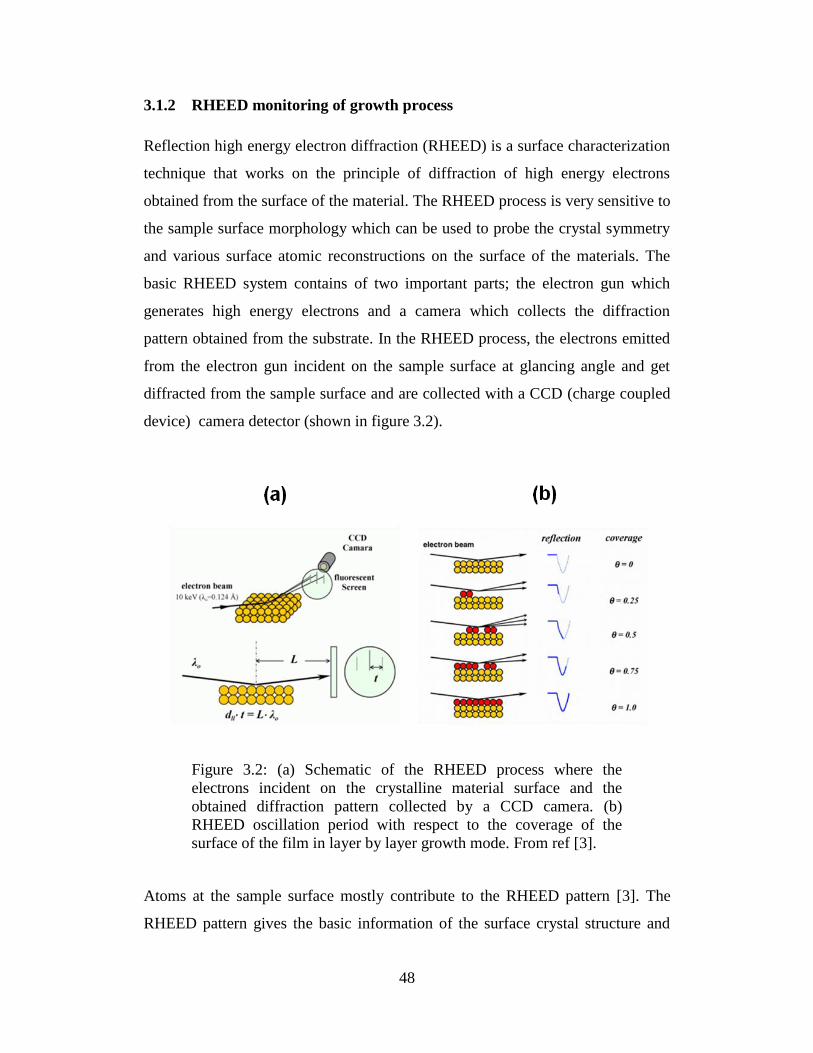
48
3.1.2 RHEED monitoring of growth process
Reflection high energy electron diffraction (RHEED) is a surface characterization
technique that works on the principle of diffraction of high energy electrons
obtained from the surface of the material. The RHEED process is very sensitive to
the sample surface morphology which can be used to probe the crystal symmetry
and various surface atomic reconstructions on the surface of the materials. The
basic RHEED system contains of two important parts; the electron gun which
generates high energy electrons and a camera which collects the diffraction
pattern obtained from the substrate. In the RHEED process, the electrons emitted
from the electron gun incident on the sample surface at glancing angle and get
diffracted from the sample surface and are collected with a CCD (charge coupled
device) camera detector (shown in figure 3.2).
Figure 3.2: (a) Schematic of the RHEED process where the
electrons incident on the crystalline material surface and the
obtained diffraction pattern collected by a CCD camera. (b)
RHEED oscillation period with respect to the coverage of the
surface of the film in layer by layer growth mode. From ref [3].
Atoms at the sample surface mostly contribute to the RHEED pattern [3]. The
RHEED pattern gives the basic information of the surface crystal structure and

49
corresponding crystal orientation. However, the most widely used application of
the RHEED process is to monitor the growth process and growth rate of the thin
film. The basic principle of the growth rate monitoring involves how the coverage
of the film surface during the growth oscillates with time. The coverage process
of the thin film surface with time for a layer by layer growth method is as shown
in the figure 3.2b. As shown in the figure the intensity of the electron diffraction
arising from the surfaces during film deposition is actually proportional to the
coverage of the surface, which follows the oscillatory behavior (during 0-50% of
coverage intensity goes down from maximum to minimum, and during 50-100%
of coverage, intensity again goes to maximum due to coverage with newly grown
layer), thus enable to monitor the growth of one complete monolayer. The minima
in intensity in this process represent the half coverage of the surface, and this
should not be misunderstood as a half unit cell growth. Therefore precise counting
of these oscillations gives the exact number of unit cells of the thin film grown
directly enabling the thickness control of the film. The growth process of
monitoring is generally performed by recording the intensity of the 0th
order spot
in the RHEED pattern. Figure 3.3 shows the RHEED intensity oscillations
obtained for the growth of LAO on STO (100) substrate. Clear oscillations allows
to control the thickness of the film (here it is 3 unit cells of LAO). The RHEED
pattern for before and after the deposition is also shown in the figure. The before
deposition pattern corresponds to the STO substrate. The spots in the patterns
represent the direct diffraction spots, which give the information of crystal planes
in reciprocal space.

50
Figure 3.3: RHEED oscillation obtained during the growth of 3
unit cells of LAO on STO (100) oriented substrates. The RHEED
patterns obtained before and after the growth of LAO on STO. The
pattern obtained for after the growth shows a streak like pattern
represent the 2D growth mode for the film with layer by layer by
growth mode.
An important observation when comparing before and after deposition patterns is
that the RHEED pattern changes from a spot like pattern before deposition to a
streak like pattern indicating the growth of 2-dimensional (2D) material on top.
The separation between these spots/streaks basically represents the spacing
between corresponding crystal planes. The analysis of the spacing will enable to
identify the crystal orientation of the film growth. A key criterion to observe
RHEED oscillations are of course material should follow the layer by layer
growth mode. Any deviation from the layer by layer growth to the so called 3D
growth will hinder this process dramatically even though the film grows epitaxial.

51
3.2. Atomic force microscopy
The important characterization techniques in the study of the thin films are the
surface morphology analysis of the samples before and after the growth. To get
the precise growth control of the thin films as discussed in the above section one
needs to start with atomically flat substrates. Atomic force microscopy (AFM) is
the most used technique to analyze the surface morphology of these substrate
material surfaces. From AFM analysis, various parameters such as surface
roughness, elemental terminations, and height profile of the specific features of
the sample surface can be obtained.
The working principle of the AFM is based on the mapping of atomic attraction
and or repulsive force between atoms on the sample surface and the AFM tip that
is attached to a cantilever. The AFM technique utilizes a short range weak
interaction forces (van der Waals). The van der Waals interaction energy of two
atoms, located on the r distance from each other can be defined from Lennard-
Jones potential equation given by
6 12
0 00( ) 2
r rU r U
r r
In this relation, the total energy (U) is composed of contributions from the long-
distance attraction forces (first term) as a result of dipole-dipole interaction
between atoms, and the short range repulsion forces (second term). The behaviour
of the above relation is shown in figure 3.4.

52
Figure 3.4: Lennard-Jones potential curve
The schematic of the AFM set up is shown in figure 3.5. The basic components in
a AFM set up are sample stage, laser diode, photo detector, cantilever with tip and
a feed back control unit that generates the equivalent image of the sample surface
morphology.
Figure 3.5: Schematic of the AFM set up with the basic
components.
53
The probe used in AFM is a sharp tip attached at the end of a cantilever. The
cantilever bends towards or away from the sample surface depending on attractive
or repulsive forces from the atoms of the sample surface. The degree of deflection
of cantilever is directly proportional to the force between the tip and the sample
and is given by
.F k Z
Here F is the force, k is the force constant of cantilever, and ΔZ is the distance
between probe and sample. The k coefficients vary in a range of 10-3
– 50 N/m.
The deflection of cantilever is used for the feedback control to adjust the Z motion
of the probe. Since the force between probe and sample is of the order of nano
Newton, a very sensitive technique is required to measure the cantilever
deflection. The laser based optical technique is used to measure the deflections.
These deflection signals are transformed in to real surface morphology using a
feed back electric current. For surface sensitive materials the AFM is used in non
contact mode also known as tapping mode, in which an AC signal applied instead.
In this mode the tip is allowed to vibrate with a specific frequency, which allows
interacting with the surface atomic forces better.
3.2.1 Substrate surface analysis
In order to obtain an abrupt interface and atomically sharp hetero structures the
first and foremost step is to start with an atomically flat substrate surface. Usually
case the purchased substrates contain a mixed termination on the surface due to
the milling and polishing steps employed. To prepare an atomically sharp
interface and to maintain stoichiometry near interfaces, a single termination
substrate surfaces are necessary. Kawasaki et al. [4] developed a Buffered hydro
florid acid (HF) chemical etching technique to get a single terminated surface for
perovskite SrTiO3 substrates, which led a foundation to create abrupt oxide
interfaces. In later years this technique was further optimized by researchers from
University of Twente [5]. In case of STO (100), using this HF treatment a specific
TiO2 termination can be achieved by the selectively etching SrO. In this process,

54
STO substrates were first ultrasonicated in DI water to form Sr hydroxide on the
surface, and then they were treated with HF for 30 seconds. In this step the
formed Sr hydroxides were selectively etches away by HF and creating a TiO2
termination (here TiO2 remains nonreactive for HF solution). This chemical
treatment then is followed by a thermal treatment step of annealing at 950 °C for
2 hours [5] in air with 5 °C per min ramping up and 3 °C per min while cooing
down.
Figure 3.6: (a) AFM topography image of the STO (100) surface
after treatment. (b) The AFM height profile showing the step
height is equal to a unit cell spacing of (100) STO of 0.39 nm. (c)
AFM topography image of the STO (110) surface after
treatment.(d) AFM height profile showing the step height is equal
to a unit cell spacing of (110) STO of 0.278 nm.
.

55
Figure 3.6a shows the topography image of STO (100) surface after treatment, the
surface contains long terraces structure with the step flow. The step height
corresponds to the unit cell height of the STO, which is actually a unit cell
distance between two successive TiO2 layers in (100) direction which is 3.905 Å.
Figure 3.6b shows the height profile of the STO(100) surface, which indicates the
step height of ~3.9 Å as expected. The terrace width depends on the miscut of the
substrates during the polishing of the surfaces. For this thesis work an atomic
smooth surfaces of SrTiO3 (110) were also prepared. Atomically smooth surfaces
were achieved by employing high temperature treatment with temperature of
1050-1100 οC with annealing time of 2 -2.5 hours. The corresponding AFM
topography image of the STO (110) surface after the treatment is shown in figure
3.6c. Figure 3.6d shows the height profile of the STO (110) surface, indicates the
step height of ~2.8 Å which is a unit cell spacing along the (110) direction. Such
treated substrates were used for the deposition of LAO/STO interface samples.
Atomically flat surfaces for substrates like LSAT and NGO were also obtained
through the above thermal treatment process.
3.3. Structural characterization
After a thin film growth it is important to check the crystal quality, growth
orientation and most importantly the chemical composition of the film. The
investigation of above mentioned properties of grown films was carried out
through X-ray diffraction, RBS experiments. In the following a brief background
to XRD and RBS techniques is given and the experimental data obtained for the
samples is also presented.
3.3.1 X-ray diffraction
X-ray diffraction (XRD) is one of the most fundamental techniques to collect the
material structure information. In the XRD process, the atomic structure of a
crystal causes a beam of X-rays to diffract into many specific directions. For fixed
wave length of incident X-rays, each diffracted angle corresponds to a specific

56
crystallographic arrangement of atomic planes of the crystal. The periodic
arrangement of atoms is generally called as atomic planes. The criterion to have
the X-ray diffraction (XRD) is known as the Bragg criterian and is given by the
equation
Here d is the spacing between the crystal atomic planes, θ is the X-ray diffraction
angle, λ is the wavelength of the X-rays, and n is the order of diffraction. The d
spacing in a crystal structure depends on the corresponding orientation and lattice
constants of a particular crystal structure which is given by
Here , , are called miller indices which gives the orientation of the atomic
planes, whereas a, b, and c are lattice constants of a crystal structure. Generally
the X-ray spectrum is obtained for diffracted x-ray intensity versus 2θ. As there
can be a series of differently-spaced planes in a crystalline material, the resultant
diffraction spectrum will consist of several peaks at the corresponding θ values.
X- ray crystallography library can be used to analyse the obtained spectrum. The
growth orientation of the film can be identified by matching the diffraction angle
of particular peak position. Once the orientation of the growth is confirmed, from
the above Brags formula one can obtain the d spacing of the atomic planes and
thereby the lattice constants of the thin film. Further the relative intensity and area
of the peak generally reflects the crystal quality of the film which can be further
precisely analyzed by performing rocking curve of a particular peak. The strain in
the thin film can also be extracted from the lattice paramenter by comparing it
with the real value.
In this study, a Bruker D8 Discover model X-Ray instrument is used. The X-Rays
generated from Cu Kα source which was operated at 40 KV and 20 mA is

57
incident on the samples mounted on a goniometer stage. The diffracted X-rays are
then collected by a detector.
Figure 3.7: (a) The XRD of the LAO/STO (100) sample with 15
nm LAO thickness. (b) The reciprocal mapping image for the
LAO/STO (100) sample with 20 uc LAO, showing a coherent
growth of LAO film on STO with a strain in LAO layers.
Figure 3.7a shows a XRD spectrum obtained for the LAO/STO (100) sample with
LAO thin film having thickness of 15 nm. A 2D detector of VÅNTEC-2000 is
used to collect the diffracted X-rays. The epitaxial growth of LAO on STO along
the (100) direction can be clearly identified from figure 3.7a. The lattice constant
of LAO is estimated from the d spacing of (100) planes to be a =3.82 Å. To
investigate the strain state in thinner LAO/STO samples, a reciprocal space
mapping (RSM) is performed on the sample with 20 uc of LAO on STO (100).
Figure 3.7b shows the corresponding RSM image of the sample, showing that
LAO is coherently grown on STO and also suggests that LAO is under tensile
strain in these thin LAO/STO samples.

58
3.3.2 Rutherford back scattering
Rutherford backscattering spectrometry (RBS) is a powerful technique for
structural and compositional characterization of thin films. Figure 3.8 shows a
schematic of RBS process.
Figure 3.8: (a) Schematic of the Rutherford backscattering (RBS)
process. (b) Typical intensity of backscattered α particles versus
energy spectrum in a RBS process.
Here a beam of mono energetic α particle (4He+2
) is generated by an electrostatic
accelerator, and directed towards the sample via magnetic steering. When the α
particles are irradiated on the sample surface, some of them are elastically back
scattered of the surface atoms, while the others enter the sample and lose some
energy along the way and are further back scattered by the atoms inside the
sample. The number and energy of these backscattered α particles are detected.
The RBS spectrum is plotted for the intensity of backscattered particles as a
function of energy. Since the collision process between α particle and atom is in
elastic, the energy (E) of the backscattered α particle is proportional to the atomic
mass (M). The intensity of spectrum at the particular energy is proportional to the
atomic mass of corresponding atoms inside the sample, thereby; the elemental
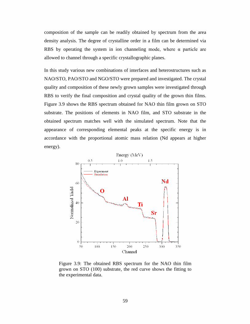
59
composition of the sample can be readily obtained by spectrum from the area
density analysis. The degree of crystalline order in a film can be determined via
RBS by operating the system in ion channeling mode, where α particle are
allowed to channel through a specific crystallographic planes.
In this study various new combinations of interfaces and heterostructures such as
NAO/STO, PAO/STO and NGO/STO were prepared and investigated. The crystal
quality and composition of these newly grown samples were investigated through
RBS to verify the final composition and crystal quality of the grown thin films.
Figure 3.9 shows the RBS spectrum obtained for NAO thin film grown on STO
substrate. The positions of elements in NAO film, and STO substrate in the
obtained spectrum matches well with the simulated spectrum. Note that the
appearance of corresponding elemental peaks at the specific energy is in
accordance with the proportional atomic mass relation (Nd appears at higher
energy).
Figure 3.9: The obtained RBS spectrum for the NAO thin film
grown on STO (100) substrate, the red curve shows the fitting to
the experimental data.
60
The composition of the thin film is further estimated from intensity spectrum
analysis, and the composition is found to be Nd0.2Al0.2O0.59 which is almost
consistent with the desired stoichiometric NdAlO3composition.The above analysis
shows that grown thin films have crystalline quality and maintain stoichiometry
during thin film growth.
Having discussed the thin film growth methodology, surface and structural
techniques and characterization of substrate and grown thin films, in the following
a brief description to the various electrical and magnetic transport measurements
that are performed on the samples will be presented.
3.4 Electrical transport measurements
A variety of electrical and magneto transport characterizations on samples were
conducted using the Physical Property Measurement System (PPMS, Quantum
Design Inc.). The PPMS system is capable of applying magnetic fields up to ± 9T,
in a 2- 400 K temperature range with a typical temperature accuracy of ± 0.5%.
Temperature can be varied with full sweep capability and ramping rates from 0.02
K/min up to 7 K/min. Temperature stability is ≤ 0.2% for temperatures ≤10 K and
0.02% for temperature >10 K. These transport measurements can also be
performed with various magnetic and current orientations to the sample by
employing a sample rotator.
The various types of electrical property measurements performed in this work are;
basic electronic characterizations including resistance versus temperature, carrier
density and mobility and their variation with temperature, magneto resistance
(MR), and electric field effects on the interface conducting channel. To perform
these electrical measurements Ohmic contacts were made by Al ultrasonic wire
bonding onto the sample (performed by West Bond wire bonder machine, with
bonding power used from 300-400 W and time of about 30 ms). Since the
deposited films mostly have a thickness of a few nanometres, thus penetration of
bonded wire from the surface to the interface due to the force allows electrically
accessing the interfaces. The Ohmic nature of the contacts is often verified by I-V
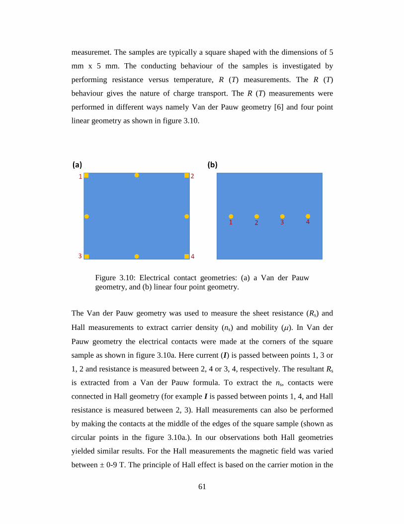
61
measuremet. The samples are typically a square shaped with the dimensions of 5
mm x 5 mm. The conducting behaviour of the samples is investigated by
performing resistance versus temperature, R (T) measurements. The R (T)
behaviour gives the nature of charge transport. The R (T) measurements were
performed in different ways namely Van der Pauw geometry [6] and four point
linear geometry as shown in figure 3.10.
Figure 3.10: Electrical contact geometries: (a) a Van der Pauw
geometry, and (b) linear four point geometry.
The Van der Pauw geometry was used to measure the sheet resistance (Rs) and
Hall measurements to extract carrier density (ns) and mobility (). In Van der
Pauw geometry the electrical contacts were made at the corners of the square
sample as shown in figure 3.10a. Here current (I) is passed between points 1, 3 or
1, 2 and resistance is measured between 2, 4 or 3, 4, respectively. The resultant Rs
is extracted from a Van der Pauw formula. To extract the ns, contacts were
connected in Hall geometry (for example I is passed between points 1, 4, and Hall
resistance is measured between 2, 3). Hall measurements can also be performed
by making the contacts at the middle of the edges of the square sample (shown as
circular points in the figure 3.10a.). In our observations both Hall geometries
yielded similar results. For the Hall measurements the magnetic field was varied
between ± 0-9 T. The principle of Hall effect is based on the carrier motion in the
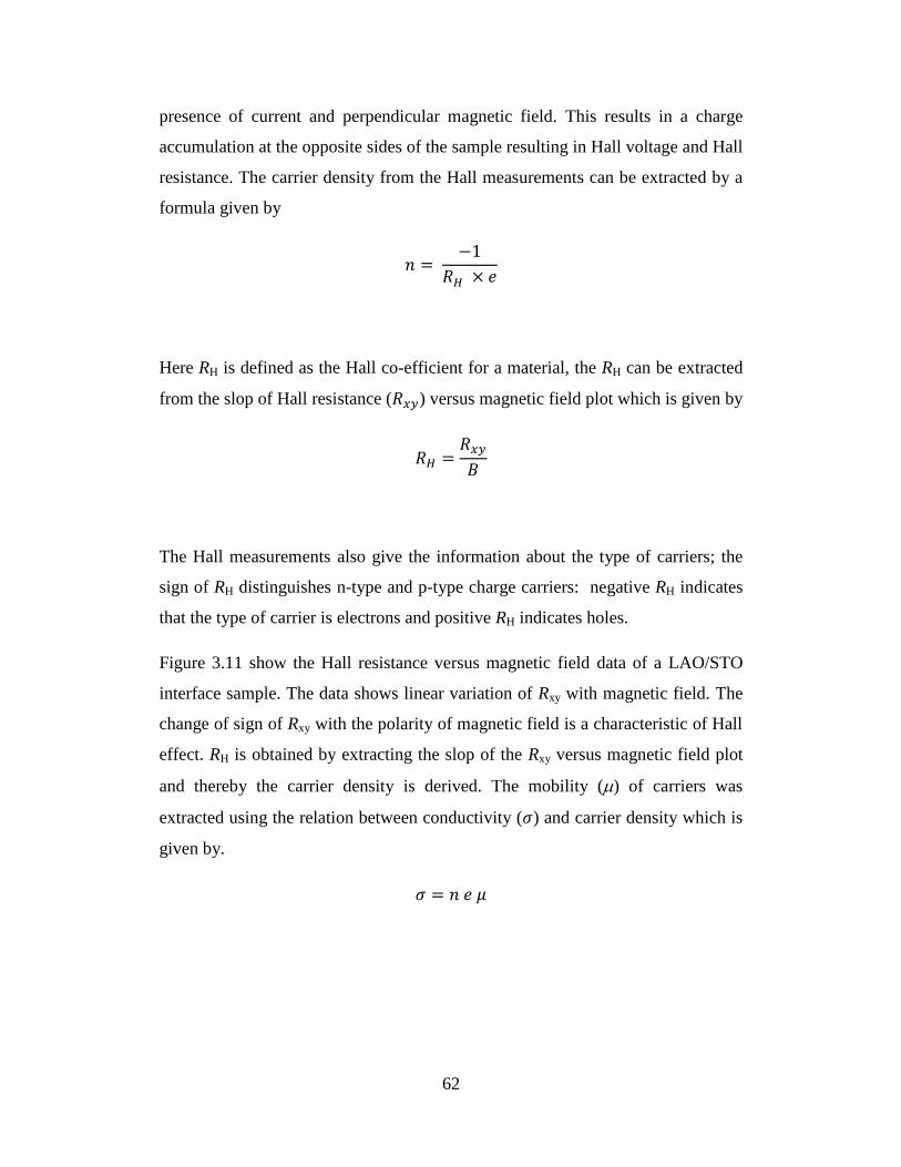
62
presence of current and perpendicular magnetic field. This results in a charge
accumulation at the opposite sides of the sample resulting in Hall voltage and Hall
resistance. The carrier density from the Hall measurements can be extracted by a
formula given by
Here RH is defined as the Hall co-efficient for a material, the RH can be extracted
from the slop of Hall resistance ( ) versus magnetic field plot which is given by
The Hall measurements also give the information about the type of carriers; the
sign of RH distinguishes n-type and p-type charge carriers: negative RH indicates
that the type of carrier is electrons and positive RH indicates holes.
Figure 3.11 show the Hall resistance versus magnetic field data of a LAO/STO
interface sample. The data shows linear variation of Rxy with magnetic field. The
change of sign of Rxy with the polarity of magnetic field is a characteristic of Hall
effect. RH is obtained by extracting the slop of the Rxy versus magnetic field plot
and thereby the carrier density is derived. The mobility () of carriers was
extracted using the relation between conductivity ( ) and carrier density which is
given by.

63
Figure 3.11: Rxy versus magnetic field performed on LAO/STO
interface.
Generally mobility characterizes the ability of charge carriers to move with in a
material. The main factor that defines the mobility is scattering time ( ) and
effective mass ( ) of the carriers (electron here).
The depends on several physical properties of the material and whereas the
effective mass depends on the band structure of the material system. Various
types of scattering mechanisms such as e-e interactions, e-phonon interactions and
a magnetic spin dependent scattering can govern the mobility of the carriers. A
distinction among these scattering mechanisms can be made by analysing the
temperature dependence of mobility.
In this study, various types of magneto resistance measurements and electric field
effect on interface conductivity were performed. To perform the magneto
resistance and electric field measurements, linear four probe geometry is used as
shown in Fig. 3.10b. The spacing between points was made sure to be equal and

64
additional care was taken to minimize the issue of misalignment of contact
geometry.
3.4.1 Magneto resistance measurements
Magneto resistance (MR) has become one of the important physical properties in
material physics ever since the discovery of giant magneto resistance in
ferromagnetic layers and colossal magneto resistance (CMR) in manganite
systems, which have found a wide range of applications in sensor technology. MR
is basically defined as the change in electrical resistance of a material when a
magnetic field is applied to the system. The magneto resistance is given by the
equation.
, are the resistance of a material with and without magnetic field,
respectively. The origin of MR arises from the influence of scattering of charge
carriers in presence of the magnetic field. Depending on the type of scattering
involved, MR is classified into various types. The MR that arises from the
Lorentz scattering of charge carriers is defined as ordinary MR. When the
magnetic field is applied on a current carrying system; electrons experience a
cyclotron motion due to Lorentz force which increases the cyclotron frequency of
the electron in its closed orbits in quantum limit. However, in a diffusive regime,
the electrons would not complete the path to a full circle due to scattering from
various scattering centers. This MR only depends on the geometry of the devices
and independent of the magnetic property and crystal symmetry of the system.
The MR in this case is always positive. Whereas the giant magneto resistance
(GMR) which originate from spin dependent scattering of electrons in adjacent
ferromagnetic layers that are separated by a metal spacer layer in presence of
magnetic field and its direction. The magnitude of GMR depends on the strength

65
of exchange interaction of electrons between these adjacent layers, is known as
Ruderman-Kittel-Kasuya-Yosida (RKKY) interaction [7-9].
In our work, properties at the LAO/STO based hetero interfaces were studied
extensively under various MR configurations. The MR experiments were
performed in various geometries namely, in-plane and out of plane.
Figure 3.12: Different MR measurement geometries: (a) Out of
plane MR. (b) In-plane MR with I and H are parallel. (c) In-plane
MR with I and H perpendicular to each other.
These geometries are defined with respect to the magnetic field and current
directions to the sample plane. Figure 3.12a shows MR geometry in out of plane
mode, were the H is applied perpendicular to the plane of the film surface; I and
H are always perpendicular to each other. In this geometry, the orbital scattering
mechanisms such as Lorentz scattering are predominant. Figure 3.12b shows the
in-plane MR mode, where the H and I are in the plane of the sample surface. As
shown, the I and H are parallel to each other which results in zero Lorentz force,
thus no orbital scattering. For magnetic systems, due to the polarization of
magnetic moments in the presence of the external H, there can be MR in this in-
plane mode due to the spin dependent scattering. Thus this in plane mode MR is a
very useful tool to distinguish orbital scatterings from magnetic spin dependent
scattering. Figure 3.12c shows geometry of measuring MR in-pane mode, where
the H and I are perpendicular to each other but both are in the plane of the sample
surface. This mode is useful to investigating the dimensionality effects of

66
conducting channel, where the orbital scattering strength depends on the
dimensionality.
The MR study can help to distinguish numerous physical phenomena. For
example, it can clearly gives the distinction among various transport mechanisms
starting from metallic, localized (magnetic Kondo scattering) and hopping
transports. This distinction can be made by performing the MR in various
geometries as described above, and from the temperature dependence of the MR.
In order to investigate the magnetism at the LAO/STO interfaces, we have
performed more specific magneto resistance measurements known as anisotropic
magneto resistance (AMR) and planar Hall effect (PHE). AMR is a relativistic
magneto transport phenomenon that arises from combined effects of spin-orbit
interaction and ferromagnetically ordered state coupled to symmetry of the
system. In AMR measurement, both I and H are always in-plane of the interface
and the angle between I and H is varied from to 36 . The origin of AMR lies
in the anisotropy of the magnetization with respect to the crystal symmetry and
spin-orbit interaction. The measurement geometries for both AMR and PHE are
shown in the figure 3.13.
Figure 3.13: Measurement and contact geometry for AMR and
PHE.

67
On the other hand planar Hall effect (PHE) is similar type of magneto resistance
measurement but it measures the transverse component of resistivity (xy). In the
PHE measurement both the I and H are in the plane of the thin film, but resistivity
measured in transverse direction.
The mathematical expressions for resistivity components, corresponding to AMR
( and PHE ( , respectively, are given by
Here and are the resistivity measured when I and H parallel and
perpendicular respectively and is the angle between I and H. However, the
above equations for AMR and PHE are applicable only for general non crystalline
and polycrystalline cases. A phenomenological model [10] used for the
interpretation of AMR in crystalline samples. The phenomenological model
includes the higher order terms in the resistivity tensor considering the symmetry
of the systems. The resistivity expression for the AMR in crystalline case is given
by MacLaurin’s series expansion of resistivity tensor as
Here , are elements of resistivity tensor of various orders, is the
direction cosines, of the magnetization, where as i and j are in any of the three
orthogonal directions. Due to the symmetry considerations most the terms vanish
and for a cubic symmetry system the above expression can be expressed as

68
Here , , are the coefficients related to the crystalline anisotropy associated
with the crystal symmetry of the system [11]. Thus the investigation of AMR and
PHE enable to explore the anisotropy of the magnetic property couple to the
crystal symmetry. Further, in magnetic systems the observed in PHE is
linked to the in-plane magnetization with a relation given by
Here is the in-plane component of the magnetization, and t is the thickness of
the film, is the constant related to anisotropic magneto resistance constant,
respectively.
In this thesis work, the investigation of AMR and PHE is carried out under
various experimental variables such as temperature, magnetic field and electric
field to the interface. These effects are analyzed with respect to the spin-orbit
interaction and crystal symmetry of the system by using the phenomenological
model discussed above.
3.4.2 Electric field effect
The electric field tuning of the electric properties at the LAO/STO interfaces has
been shown to create several novel phenomena such as insulator-metal transition
and tunable ground state of two-dimensional superconductivity. The external
electric field applied to a material attracts or repels charge carriers, resulting in
charge accumulation or depletion from the channel modifing the electric
properties dramatically. The characteristic width of the accumulation or depletion
regimes is given by the electro static screening length el, is also called as
Thomas–Fermi length. To have feasible electric field effects large screening
lengths are needed i.e effectively 2D system. Conventional metallic systems have
very short length scales due to the large carrier densities in the order of 1015
cm-2
and therefore negligible field effects were observed [12]. On the other hand

69
LAO/STO interfaces have carrier densities in the order of 1013
cm-2
with
dimensions of the conducting channel of few a nanometres which make them
ideal for field effect studies. The polarization ( ), or areal carrier density (charge
cm-2
) that can be induced at given gate voltage VG applied across an gate
insulator of thickness t is given by
Here is the relative dielectric permittivity of the gate dielectric material. The
above equation suggests that there can be two ways to increase the electric field
effects either by applying large gate voltage or to use a large gate material.
In this thesis work, the properties of the 2DEG at the LAO/STO interfaces have
studied extensively under the applied electric field. These gating measurements
were further utilized in the investigation of properties such as spin-orbit
interaction and AMR studies.
Figure 3.14: Schematic of the electric field effect measurement
configuration for the LAO/STO interface sample.

70
The 2D carrier confinement and tunable carrier density at the LAO/STO
interfaces enable to tune the interface properties. The Schematic of the electric
field effect device configuration for the LAO/STO interface samples is shown in
the figure 3.14. The electric field effect measurements on LAO/STO interfaces
were performed by applying the electric potential (voltage) to STO which is used
as the gate material. STO (back gate) is preferred over LAO (top gate) due to the
large dielectric constant of 10,000 at low temperature. This unusual dielectric
response of STO at low temperatures let to show the pronounced electric field
effect on LAO/STO interfaces. The back electrode for the STO is provided by
applying Silver (Ag) epoxy to the STO back surface. During this gate electrode
preparation, precautions were taken to avoid any lateral conduction that leaks the
charge to the interface. The leakage currents were monitored through a source
meter and it was made sure that it is below 1 nA (nano Ampere) during the
measurements. The source terminals (I-) of the channel are made as common
terminal for both gate (-VG) and channel. The electric contacts for the channel
were made through Al wire bonding to the interface. The Ohmic nature of the
contacts was verified through I-V measurements. Linear probe contact geometry
is used for conventional resistance measurements and Hall geometry is employed
for carrier density measurements. In this study the gate induced electric field
effects are performed in the investigation of the spin-orbit interaction. In the
following a brief introduction to the spin-orbit interaction is given.
71
References:
[1] D. Dijkkamp, T. Venkatesan, X.D. Wu, S.A. Shaheen, N. Jisrawi, Y.H.
Min-Lee, W.L.McLean, M. Croft, “Preparation of Y‐Ba‐Cu oxide
superconductor thin films using pulsed laser evaporation from high Tc bulk
materials,” Appl. Phys. Lett. 51 619 (1987).
[2] X.D. Wu, T. Venkatesan, A. Inam, X.X. Xi, Q. Li, W.L. McLean, C.C.
Chang, D.M.Hwang, R. Ramesh, L. Nazar, B. Wilkens, S.A. Schwartz,
R.T. Ravi, J.A. Martinez, P.England, J.M. Tarascon, R.E. Muenchausen,
S. Foltyn, R.C. Estler, R.C. Dye, A.R.Garcia, N.S. Nogar, “Pulsed laser
deposition of high Tc superconducting thin films: present and future,”
Mater. Res. Soc. Symp. Proc. 191, 129 (1990).
[3] http://www.material.tohoku.ac.jp/~kaimenb/e_genri.html#heed.
[4] M. Kawasaki, K. Takahashi, T. Maeda, R. Tsuchiya, M. Shinohara, O.
Ishiyama, T. Yonezawa, M. Yoshimoto, H. Koinuma, “Atomic control of
the SrTiO3 crystal surface,” Science, 266, 1540-1542 (1994).
[5] G. Koster, B. L. Kropman, G. J. H. M. Rijnders, D. H. A. Blank, and H.
Rogalla, “Quasi-ideal strontium titanate crystal surfaces through formation
of strontium hydroxide,” Appl. Phys. Lett, 73, 2920-2922 (1998).
[6] L. J. van der Pauw, “A method of measuring the resistivity and Hall
coefficient on Lamellae of arbitrary shape,” Philips Technical Review, 20,
220-224 (1958).
[7] M.A. Ruderman and C. Kittel, “Indirect Exchange Coupling of Nuclear
Magnetic Moments by Conduction Electrons”, Phys. Rev. 96, 99 (1954).
[8] T. Kasuya, “A Theory of Metallic Ferro- and Antiferromagnetism on
Zener's Model”, Prog. Theor. Phys. 16, 45 (1956).
[9] K. Yosida, “Magnetic properties of Cu-Mn alloys”, Phys. Rev. 106, 893
(1957).
72
[10] T. R. McGuire, and R. I. Potter, “Anisotropic magneto resistance in
ferromagnetic 3d alloys”, IEEE Trans. Magn. 11, 1018 (1975).
[11] C. R. Hu, J. Zhu, G. Chen, J. X. Li, Y. Z. Wu, “Fourfold symmetry of
anisotropic magnetoresistance in epitaxial Fe3O4 thin films,”
arXiv:1105.5781.
[12] C. H. Ahn, J. –M. Triscone, and J. Mannhart. “Electric field effect in
correlated oxide systems,” Nature 424, 1015-1018 (2003).

73
Chapter 4
Investigation of carrier confinement and electric field effects
on magnetic interactions at the LaAlO3/SrTiO3 interfaces
Abstract
In this chapter, the electric and magnetic properties at the LAO/STO (100)
interface are investigated under various growth parameters such as LAO layer
thickness and oxygen pressure during growth. The LAO/STO interfaces show
insulator to metal transition with critical LAO thickness, and a thickness
dependence localization behavior. In order to probe the magnetic ordering and its
possible anisotropy with crystallography, the magnetic interactions at the interface
are investigated through specific anisotropic magneto resistance (AMR) and
planar Hall effect (PHE) measurements on LAO/STO (100) interfaces and
heterostructure of LAO/STO grown on NdGaO3 (110) substrates. These
measurements were performed as a function of magnetic field, temperature and
electric field which reveal the presence of the predominant magnetic interactions
at the LAO/STO interfaces. Specifically fourfold oscillation in the AMR and large
PHE are observed. The carrier confinement effects on the AMR are evaluated and
it is found that the fourfold oscillation appears only for the case of 2DEG samples
while it is twofold for the 3-dimensional case. The fourfold oscillation fits well to
the phenomenological model for a cubic symmetry. Thus this oscillation behavior
is attributed to the anisotropy in the magnetic scattering arising from the
interaction of itinerant electrons with the localized magnetic moments coupled to
the crystal symmetry. The AMR behavior is further found to be sensitive to
applied gate electric field, emphasizing the significance of spin-orbit interaction at
the interface. These confinement effects suggest that the magnetic interactions are
predominant at the interface, and the gate electric field modulation of AMR show
the possibility for electric field tuning of magnetic interactions. The observed

74
large PHE further indicates that the in plane nature of magnetic ordering arises
from the in-plane Ti 3dxy orbitals.

75
4.1. Introduction
As discussed earlier the growth parameters and conditions of the LAO/STO
interfaces are very crucial for the properties of the interfaces such as insulator-
metal transition with LAO layer thickness, superconductivity and magnetism with
oxygen pressure during growth. In spite of the extensive research, a clear picture
of interplay between these electronic and magnetic phenomena and the growth
parameters and sample configurations is less understood. In this chapter, the
electric and magnetic properties at the LAO/STO (100) interface are investigated
under various growth parameters such as LAO layer thickness and oxygen
pressure during growth, which can be used to control the degree of carrier
confinement at the interface.
With this frame work, several LAO/STO interface samples were prepared under
different growth parameters. First, the electrical transport properties of the
LAO/STO interfaces are investigated, which includes the dependence of the
interface conductivity to the LAO thickness and growth oxygen pressure. To
investigate the nature of magnetic interactions in the LAO/STO based hetero
interfaces, detailed magneto resistance measurements were carried out on several
samples under various parameters such as growth oxygen pressure, confinement
of electron gas, and electric field. The results for the electric and magnetic
interactions at the interface are discussed in the carrier confinement picture.
4.2. Transport properties of the LaAlO3/SrTiO3 (100) interfaces
4.2.1 LaAlO3 thickness dependence
For the LAO layer thickness dependence study, LAO/STO (100) interface
samples with various LAO layer thicknesses were prepared using PLD by
ablating LAO target onto the TiO2 terminated STO (100) substrate. The growth
oxygen pressure (PO2) for the samples during the deposition was fixed at 1×10⁻³
Torr. The growth temperature was set to be 720 oC. Precise control of the
thickness of LAO is achieved by RHEED monitoring. Transport and Hall effect

76
measurements were performed on the samples using standard van der Pauw
geometry from which carrier density (ns) and mobility () of the samples were
extracted.
Figure 4.1 shows the variation of room temperature conductivity and the ns as a
function of number of LAO unit cells (uc).
Figure 4.1: Room temperature conductivity and carrier density, ns
of LAO/STO samples as a function of number of LAO unit cells.
Clearly, a distinguishable insulator-to-metal transition in conductivity is found for
the samples at about LAO thicknesses of 3-4 uc. The change in conductivity is
more than 3 orders of magnitude between the conducting and insulating states
(instrument measurement limit). Simultaneously, the ns also changes almost 3
orders of magnitude across the insulator-to-metal transition. Above the critical
thickness of 4 uc, the ns saturates at a value of the order of 1013
cm-2
. This
insulator-to-metal transition behavior is found only to depend on the thickness of
the LAO layers and independent of deposition time (i.e. growth rate of LAO
layers). The property of insulator to metal transition at the LAO/STO interface

77
was first reported by Thiel et al. [1]. J. Levy and co-researchers exploited this
property for nano-scale charge writing by conducting AFM, where the insulating
ground state of a 3 uc sample is manipulated and transformed into a metallic state
locally by applying gate voltage to the interface through AFM tip [2].
However, for the samples with thicker LAO layers (> 3 uc) a slight decrease is
observed in both conductivity and ns. To understand this behaviour the
temperature dependence of the sheet resistance Rs (T) for the LAO/STO interface
samples with various LAO thicknesses was measured in the temperature range
between 300 to 2 K. As shown in figure 4.2, the sample with LAO thickness of 4
uc shows a typical metallic behavior with Rs decreasing throughout the
temperature range down to 2 K with Rs is about 200 Ω at 2 K, albeit with small
localization (upturn in Rs) at low temperatures.
Figure 4.2: The Rs (T) behavior of the LAO/STO samples with
various LAO thicknesses.
It is found that these thinner LAO samples have often become superconducting at
mK temperatures with relatively higher mobility and they also favorable for

78
quantum transport. However, as the thickness of LAO increases the samples start
to show the localization behavior from weak (8, 12 uc samples) to strong (20 uc)
localizations. In these samples, the Rs at 2 K are also found to increase with the
increase in LAO thickness. The sample with 20 uc LAO thickness shows a
dramatic effect of localization. The 20 uc sample show measurable Rs only up to
20 K with the resistance in order of ~MΩ indicating strong localization of
electrons and this result in an insulating state below 20 K. The transport properties
presented above are consistent with the published literatures [1, 3]. In the
following, the properties of LAO/STO interface are investigated with respect to
the samples growth oxygen pressure.
4.2.2 Growth oxygen pressure dependence
To investigate the effect of growth oxygen pressure (PO2) dependence on the
LAO/STO interface properties, samples were grown in different PO2 ranging from
1×10⁻⁵
to 5×10⁻³
Torr with a fixed LAO thickness of 8 uc on TiO2 terminated
SrTiO3 (100) substrates. Figure 4.3a shows the Rs (T) behavior for the
corresponding samples. The samples grown with PO2 1×10⁻⁴
Torr show the
typical metallic behavior with room temperature Rs of about 20 KΩ. On the other
hand the sample grown at low PO2 of 1×10⁻⁵
Torr shows metallic behavior but
with very low Rs of about 20 Ω at room temperature, a 3 order of magnitude drop
in resistance compared to the high PO2 samples. The PO2 dependence of Rs(T)
shown here is consistent with earlier reports [4, 5]. Stronger effects of growth PO2
can be seen in the ns dependence with temperature for the corresponding samples
shown in figure 4.3b.

79
Figure 4.3: Temperature dependence of transport properties of
LAO/STO samples grown at different oxygen pressures. (a) Sheet
resistance, Rs (T). (b) Carrier density, ns (T). (c) Mobility, (T).
For the high PO2 samples, the ns is of the order of 5-8 ×10¹³
cm-2
at 300 K and
about ~2-3×10¹³
cm-2
at 2 K, whereas for the low PO2 (1×10⁻⁵
Torr ) sample the ns
is about 9×10¹⁵
cm-2
at 300 K and 6×10¹⁵
cm-2
at 2 K. The large ns observed in
low PO2 sample arise from the creation of oxygen vacancies due to the surface
reduction in STO itself. Figure 4.3c shows the temperature dependence mobility,
(T). For the high PO2 samples, the is of the order of 5 cm2 V
-1 s
-1 at 300 K and
1000 cm2 V
-1 s
-1 at 2 K, whereas for the low PO2 sample the is about 30 cm
2 V
-1
s-1
at 300 K and 50,000 cm2 V
-1 s
-1 at 2 K showing the high mobility nature of the
low PO2 2 grown samples.
Based on the above observation the growth regime can be divided in to three
regimes. The PO2 range of 1×10⁻⁵
Torr or less is called the low pressure regime.

80
Samples prepared in this regime produce a three-dimensional (3D) like
conductivity with ns in the order of 1016
cm-2
. Further, these samples generally
show a Fermi liquid type metallic behavior and often undergo superconductivity
at mK temperatures. The samples grown in intermediate PO2 ranges of 1×10⁻³
to
1×10⁻⁴
Torr generally tend to show the magnetic character with localization
effects and also low temperature superconductivity. However, the samples
deposited under PO2 above 1×10⁻³
Torr produce pronounced magnetic effects with
strong localization. These high PO2 grown samples produce strictly two-
dimensional (2D) conductivity with ns of the order ~1013
-1014
cm-2
. The character
of the dimensionality of the carriers described above was investigated and
confirmed by a conducting AFM experiment on a cross-section of the LAO/STO
interface by Basletic et al. [6] where it is found that the dimensionality of the
conducting channel is micrometers for the 3D case, and a few nanometers for 2D
case. The above dimensionality observations have been investigated further
through magneto resistance experiments [7] and this shows that dimensionality is
one of the parameters that can be utilized to control the properties of the electron
gas.
4.3. Magnetic interactions at the LaAlO3/SrTiO3 interface
One of the fascinating properties that emerged from PO2 phase diagram is the
magnetism at this non-magnetic LAO/STO interface. The magnetic effects were
first reported by Brinkman et al. [5] with a signature of Kondo effect in samples
prepared at relatively higher PO2. Subsequently, Ariando et al. [8] reported
electronic phase separation at this interface by exploiting specific STO surface
preparations and PO2 and it is shown that the strength of the magnetism depends
on growth PO2. Further, the magnetic origin at this interface is confirmed by direct
imaging of magnetic patches using scanning SQUID [9].
One common issue with the magnetism is anisotropy. Has the magnetic moment
has specific crystallographic preference? In scanning SQUID experiment [9], the
magnetic moment distribution near the interface is examined and a signature of

81
some forms of anisotropy within the plane of interface is found. However, no
information about the anisotropy with respect to crystallographic symmetry is
found. The origin of the magnetism in the LAO/STO interface is believed to be
arising from the localized 3d orbitals. Owing to the preferential occupancy,
particularly to the Ti 3dxy orbitals at the interface, various reports have presumed
that the magnetization predominantly is in the plane of interface [8-10]. The
magnetism arising from 3d orbitals can show a tendency of crystallographic
anisotropy due to strong spin-orbit interaction. Thus investigation of anisotropy of
magnetic ordering in this system is necessary to map the magnetic phase diagram
at the interface.
An effective alternative way for probing these low dimensional and relatively
weak magnetic interactions is by the magneto transport measurements. Recently,
Dikin at al. [11] investigated the magnetic order at the LAO/STO interfaces
through in-plane magneto resistance (MR) measurements and showed a hysteresis
behavior in the resistance with magnetic field which is a signature for the
presence of magnetic ordering. A natural way to further probe this magnetic
anisotropy is by investigating the angle dependence of in-plane magneto
resistance, i.e., anisotropy magneto resistance (AMR) and planar Hall effect
(PHE), which directly relate to the magnetic scattering of itinerant electrons
associated with the spin-orbit interaction in the system. The LAO/STO interface
exhibits a strong spin-orbit interaction [12] due to the broken symmetry near the
interface.
In the following a detailed study of various in-plane MR measurements performed
on the LAO/STO samples prepared under various PO2 is presented (These
pressure dependence samples correspond to those shown in figure 4.3). First,
comprehensive MR data (including AMR and PHE) is presented for the
LAO/STO interface sample deposited at 1×10⁻⁴
Torr. These MR measurements
were performed with respect to various parameters such as magnetic field,
temperature and gate electric field. The results are further compared with the
AMR data obtained for the LAO/STO samples prepared at low as well as high

82
PO2, and with that of LAO/STO heterostructure grown on NGO(110) substrate.
The acquired data is interpreted with respect to carrier confinement effects on
magnetic interactions.
4.3.1 In-plane magneto transport
The in plane magneto transport measurements are summarized in figure 4.4.
Figure 4.4: Magneto transport properties of LAO/STO interface
simple prepared at 1×10⁻⁴
Torr. (a) The Rs (T) measured with the
in-plane magnetic field of 0 and 9 T. (b) In-plane magneto
resistance (MR) measured with fixed angle (θ =0ο, 90
ο)
between I and H at 2 K and 9 T.
Figure 4.4a shows Rs (T) measured for the LAO/STO sample deposited at 1×10⁻⁴
Torr (LAO thickness of 8 uc) with 0 and 9 T magnetic fields applied in-plane to
the interface. For the 9 T case, the Rs starts to deviate (decrease) from 0 T case at
temperatures at about 25 K, indicates a negative MR. The negative MR is a
signature of a spin dependent magnetic scattering. The contribution from
conventional orbital and Lorentz scattering to this MR can be excluded as the
measurement is performed in in-plane mode, where the Lorentz forces are
negligible. Figure 4.4b shows the MR measured at 2 K in two different in-plane
modes (I || H, and I H), which clearly show the negative MR in both cases.
There appears a critical magnetic field above which the MR starts to change

83
significantly. The significant difference in MR behavior between these two
measurement modes is the change in the critical magnetic field, with critical fields
for I || H, and I H modes are 1.5 T and 3 T respectively. The origin of this
behavior could due to the additional contribution from orbital scatterings
specifically in I H mode. These in-plane MR measurements confirm the
presence of magnetic interactions at the LAO/STO interface. The anisotropy
property of these magnetic interactions is further investigated through precise in-
plane magneto transport measurements namely, AMR and PHE that are discussed
in the following.
4.4 Anisotropic magneto resistance and planar Hall effect at the
LaAlO3/SrTiO3 interface
Figure 4.5: Schematic of AMR measurement geometry.
In anisotropic magneto resistance (AMR) measurement, both the magnetic field
(H) and current (I) are in the plane of the sample, and the angle between H and I
is varied from 0° to 360°. Here, I is fixed along the <100> crystallographic
direction (schematic depicted in figure 4.5). Here the AMR is defined as

84
AMR=(R()-R (0)/R(0)) ×100%, is the angle between H and I, and R(0) is the
resistance when H and I are parallel to each other.
4.4.1 Magnetic field and temperature dependence of AMR
The AMR is investigated first with respect to the magnetic field and temperature.
Figure 4.6a shows the AMR measured at 2 K with varying H from 3 to 9 T on the
LAO/STO sample grown at 1×10⁻⁴
Torr.
Figure 4.6: (a) AMR measured at 2 K with varying magnetic field
3-9 T. (b) AMR measured at 9 T with varying temperature for the
LAO/STO interface sample grown at 1×10⁻⁴
Torr.
From the figure 4.6a it is clear that AMR shows a significant variation with
respect to the angle between H and I. For the AMR measured at 9 T, a clear
fourfold oscillation (AMR oscillation with angle showing four minima/maxima
between 0° and 360°) is observed with resistance minima appears at an angle 45°
85
to the principal 100 directions are repeats every interval of 90°. When H is
decreased, a clear decrease in the amplitude of the fourfold oscillation and
simultaneously a gradual transformation from fourfold to twofold (AMR with two
minima/maxima) oscillation are observed. At H=3 T, the oscillations turn
completely into twofold with resistance maxima appear at 90° and 270° with an
interval of 180°. A noticeable observation here is the change of the AMR sign
from negative for the fourfold oscillation to positive for the twofold oscillation.
The AMR variation is further measured with respect to temperature. Figure 4.6b
shows the AMR measured with varying temperature from 2 to 20 K at H=9 T. In
this case, the fourfold oscillation in the AMR gradually decreases when the
temperature increases and simultaneously a twofold oscillation emerge at higher
temperatures. At 20 K the AMR start to transform into a twofold behavior. A
similar kind of oscillation behavior in AMR has been previously reported in
magnetic systems such as manganites [13-16] and Fe3O4 [17]. Very recently, a
signature of AMR is also observed at the LAO/STO interfaces [18, 19].
Strikingly, all the above mentioned systems possess d-orbital characters. This
suggests that the magnetic interactions arising from the d-orbitals is crucial for the
observed fourfold oscillation.
A phenomenological model is widely used to quantitatively describe the AMR
and PHE in various systems [20, 21]. This model is used to explain the AMR
behavior in several 3d ferromagnetic magnetic systems (details of the model are
discussed in chapter 3). In this model, the resistivity tensor is expressed in terms
of the direction of current with respect to the applied magnetic field. The fourfold
oscillation behavior in the AMR is suggested to be arising from the contribution
of higher order terms in the resistivity tensor relating to the crystal symmetry of
the system [20]. For the cubic symmetry system, the variation in resistance with
angle () is expected to follow the equation containing direction cosines of higher
order given by:

86
Here corresponds to the AMR whereas to the PHE. The
coefficients , and are to arising from the uniaxial and cubic components
of magnetization and and are additive constants introduced to take the
observed asymmetry in the magnitude in the four oscillations into account. Figure
4.7a shows a fitting for the experimental AMR data measured at 2 K and 9 T by
equation 1, showing a good agreement with the above formula. Onether striking
observation is the asymmetry in the magnitudes between the maxima or minima
in the fourfold oscillation. If one considers just the crystalline anisotropy then
symmetric amplitudes are expected. However, the fact that we see a strong
asymmetry strongly suggests that there is further uniaxial anisotropy present in
the system.
Figure 4.7: (a) A phenomenological model formula fit to the AMR
obtained at 9 T and 2 K. (b) Sin2 fit for the AMR obtained at 3T
and 2 K.
Such anisotropy with respect to the crystal symmetry probably arises because of
Fermi surface reconstruction of the various 3d orbitals at the interface. The good
agreement of experimental data with the model implies the predominant role of
crystal symmetry on the magnetic interactions at the LAO/STO interface.
Further, the twofold oscillation in AMR observed at 2 K and 3 T is found to
follow a sin2 dependency. The corresponding sin
2 fit for the twofold oscillation

87
is shown in figure 4.7b which matches the experimental data accurately. The
origin of the twofold oscillation can be from the Lorentz scattering of charge
carriers which follows the sin2 dependency. The transformation of the fourfold
to twofold oscillations infers that there are two competing components (spin and
charge scatterings) for the AMR, and their contribution to AMR depends on
parameters such as magnetic field and temperature. The evolution of fourfold
oscillation from twofold oscillation for the magnetic field H > 3 T implies that a
critical field strength is needed for of the coherent magnetic scattering to
overcome the charge scattering. Furthermore, the signature of the four fold AMR
starts to diminish for higher temperatures (above 20 K) which could be due to the
diminishing of coherence scattering as thermal fluctuations become dominant.
4.4.2 Current dependence of AMR
The AMR was further investigated by varying the magnitude of the current (I).
Figure 4.8 shows the corresponding AMR behavior measured at 2 K and 9 T for
the I ranging from 0.5 µA-0.5 mA. The data clearly shows that the observed
fourfold oscillation behaviour has no I dependence. This explicitly rules out the
possibility of contribution from any activated carrier behavior due to the
continuous application of I and possible thermal effects on sample to the observed
AMR behavior. It implies that the orientation and magnitude of the magnetic
fields are the only key parameters in the observed AMR.

88
Figure 4.8: AMR measured with different magnitudes of current
(I) for the LAO/STO interface sample prepared at 1×10⁻⁴
Torr at 2
K and 9 T.
4.4.3 Electric field effect on AMR
Figure 4.9: AMR measured with various back gate voltages at 3 K
and 9 T for the LAO/STO interface prepared at 1×10⁻⁴
Torr.

89
At the LAO/STO interfaces, the electric field applied to the interface through
back gate voltage was shown to tune the spin-orbit interaction [12] and also the
carrier density modulation which is further interpreted to influence the
preferential d-orbital filling [22]. To examine the influence of spin-orbit
interaction on AMR, the gate electric field dependence of the AMR measurements
were performed on the LAO/STO sample grown at 1×10⁻⁴
Torr. Here the gate
voltages were applied to the interface through STO substrate as the back gate
dielectric material. Figure 4.9 shows the gate electric field dependence of the
AMR behavior measured at 3 K and 9 T. As shown in the figure 4.9 for the +30 V
gate voltage the strength of the fourfold oscillations is enhanced compared to the
+0 V case. On the other hand, the fourfold oscillation in AMR turns into a
twofold for the -30 V, showing the distinct effects of gate electric field at these
interfaces. It suggests that the gate tunable spin-orbit interaction may be the key in
the observation of the AMR behaviour. One possibility for this AMR change is
due to the specific orbital fillings, especially the inplane dxy orbitals. The
modulation of AMR with electric field effects provides an opportunity to tune the
magnetic interactions by electric field at these interfaces. Another effect of an
electric field is carrier modulation through accumulation or depletion of charge at
the interface, and this may induce the change in the orbital fillings, and spin-orbit
interaction at the interface. The applied electric fields are able to induce ns of
about ~1013
cm-2
. Recently, Joshua et al. [22] showed that a critical ns exist for the
LAO/STO interfaces where the preferential occupancy of 3d-orbitals is different
below and above this critical ns. This case may applicable in our samples also;
however the critical ns values may also depend on the mobility of the sample. The
modulation of AMR with electric field effects further confirm the interface effects
to have a key role to the magnetic interactions and it provides an opportunity for
tuning the magnetic interactions with electric fields via spin-orbit interaction. It is
to note that step edges at the LAO/STO interfaces may contribute to the in plane
anisotropy, it is shown that step edge effect follows a sinusoidal dependency with
the step edge direction [23]. However, our data show higher order anisotropy with
four fold behaviour of a square and fourth power of Cosine function, ruling out

90
the step edges as the prime origin. Moreover the observed electric field, magnetic
field and temperature dependence of AMR can not be explained by the step edge
scattering mechanism.
4.4.4 Planar Hall effect
To further understand the anisotropy planar Hall effect (PHE) measurements were
performed. The PHE is similar to the AMR, which arises from magnetic related
anisotropy. In PHE measurements, I and H are in the plane of the sample and the
angle between H and I is varied between 0° to 360°. Unlike the AMR, here the
resistivity is measured using Hall geometry, i.e., transverse resistance, ,
(depicted in figure 4.10).
Figure 4.10: Schematic of PHE measurement geometry.
PHE is a very useful technique to investigate magnetism especially for systems
which have predominant in-plane magnetizations, in which the perpendicular
anomalous Hall effect is difficult to be obtained due to weak magnetism. Figure
4.11a shows Rxy measured at 9 T with respect to angle () at various temperatures.
The maxima (positive signal) and minima (negative signal) in appear at 45°

91
to the principal 010 directions with 90° interval. The sign change of Hall signal
with angle is a characteristic of PHE. In general, the PHE ( ) is expected to
follow sin 2θ behavior [24, 25]. Figure 4.11b shows a fit to sin 2θ for the PHE
measured at 2 K and 9 T, which is in fair agreement with the formula (equation 2)
with a slight deviation from the formula with 180° interval. This might be from
the contribution of misalignment or contribution from the perpendicular
component of MR.
Figure 4.11: (a) PHE measured at 9 T with various temperatures
for the LAO/STO interface prepared at 1×10⁻⁴
Torr. (b) Sin 2θ fit
for the PHE obtained at 2 K and 9T.
We note here is that the AMR can be fourfold and/or two fold, but PHE is only
twofold. This is consistent with the phenomenological theory by considering
cubic symmetry of the system [20, 21]. The large planar Hall signal observed here
infers a strong in plane component of magnetic ordering at this interface.
The above experiments give enough hints that magnetic interactions are very
sensitive to the interface parameters related to carrier density and interface
parameters such as spin-orbit interaction. The carrier confinement of the two
dimensional electron gas near the interface does influence the preferential
occupancy of the Ti 3d orbitals near the interface. Moreover the strength of the
spin-orbit interaction near the interface is expected to be strong due to the broken

92
symmetry effects. However thus far, the interplay between these magnetic
phenomena and carrier confinement is less explored at these interfaces. It is noted
here that in this PO2 growth regime (where we observed the fourfold oscillation in
AMR) various reports have demonstrated interface magnetism using various
techniques. The strength of the magnetic interaction is shown to be sensitive to
sample growth parameters. In the following section we present AMR performed
on various samples that include LAO/STO interfaces prepared at different growth
PO2 and LAO/STO heterostructure grown on NGO (110). The objective of this
work is to investigate the different sample configurations and carrier confinement
effects on the AMR and thereby on magnetic interactions.
4.4.5 Carrier confinement effects on AMR
Figure 4.12: AMR measured at 9 T with varying temperature for
the LAO/STO interface sample grown at 1×10⁻³
Torr.

93
Figure 4.12 shows the AMR measured on the sample grown at 1×10⁻³
Torr with
varying temperature from 2 to 20 K at H=9 T. For the AMR measured at 2 K, the
resistance minima appearing at an angle 45° to the principal 100 directions,
however with a repetition interval of 180°.
In comparison, there are subtle differences observed from the previous sample
(which is grown at 1×10⁻⁴
Torr). At 2 K and 9 T, the 1×10⁻³
Torr grown sample
show further preferential anisotropy, where the magnitude of the AMR is negative
at only two angle positions (45° and 135° ) instead of four and as the temperature
increases the four fold oscillations start to become isotropic with a repetition
interval of 90°. Note here that although the carrier density of these two samples is
identical (2.4×10¹³
cm-2
from figure 4.3b) yet the AMR shows distinct differences
suggesting that interface parameters are very crucial. The most important
parameters in this case are the spin-orbit interaction, carrier confinement and
interface ground state. From the results presented above it is clear that the samples
having 2D confined electron gases show strong anisotropy in AMR with fourfold
oscillations.
To further investigate the effect of the confinement of the electron gas to the
anisotropy, AMR measurements were performed on a LAO/STO sample grown at
1×10⁻⁵
Torr (low PO2 sample) which has 3D like conducting channel (the spread
of electrons deep in to the STO). Figure 4.13 shows the AMR measured at 9 T
with varying temperatures for the corresponding sample.
Remarkably, in contrast to high PO2 samples, it shows only twofold oscillation
throughout the temperature range of 2-20 K. However, an anti symmetric
behavior in AMR is noticed between 0° to 180° and 180° to 360° at low
temperatures and it gradually decreases with increasing temperature suggesting
the intrinsic origin for this anti symmetry. This antisymmetry can be attributed to
the difference in inter boundary scattering. While the electrons scattered toward
the interface encounter a sharp boundary at the interface, those scattered into the
STO side will see a relatively graded boundary due to the 3D nature of the
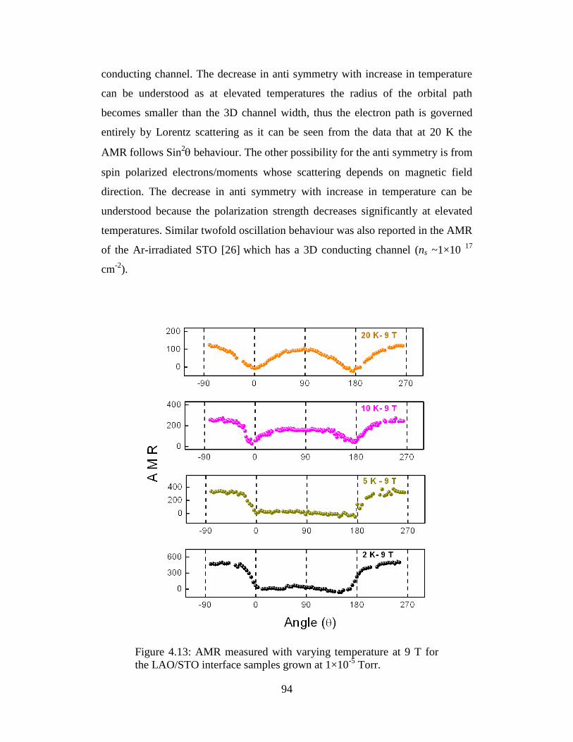
94
conducting channel. The decrease in anti symmetry with increase in temperature
can be understood as at elevated temperatures the radius of the orbital path
becomes smaller than the 3D channel width, thus the electron path is governed
entirely by Lorentz scattering as it can be seen from the data that at 20 K the
AMR follows Sin2 behaviour. The other possibility for the anti symmetry is from
spin polarized electrons/moments whose scattering depends on magnetic field
direction. The decrease in anti symmetry with increase in temperature can be
understood because the polarization strength decreases significantly at elevated
temperatures. Similar twofold oscillation behaviour was also reported in the AMR
of the Ar-irradiated STO [26] which has a 3D conducting channel (ns ~1×10
17
cm-2
).
Figure 4.13: AMR measured with varying temperature at 9 T for
the LAO/STO interface samples grown at 1×10⁻⁵
Torr.

95
To validate the confinement effects, LAO (15 uc)/STO (8 uc) interface was
prepared on NdGaO3 (110) substrate a technique employed recently to grow
2DEG on different substrates [27]. The sample shows a metallic behavior with
localization behavior at low temperatures. The NdGaO3 substrates are highly
insulating and thus in this case the electron gas is confined in STO layers of 8 uc
thick. Figure 4.14 shows the AMR measured at 9 T with varying temperature (2-
20 K) for the corresponding sample. Evidently, here also a fourfold oscillation is
observed in the AMR.
Figure 4.14: AMR measured with varying temperature at 9 T for
the LAO/STO interface grown on NGO (110) substrate.

96
Further the magnitude of AMR gradually diminishes as the temperature increases.
This sample shows a clear fourfold oscillation even up to 20 K suggesting that
these heterostructures might have pronounced magnetic effects due to the strain
states at the interface. As the conducting channel is confined to within 8 uc, thus
the strong interface effects are also expected here similar to the high PO2 grown
LAO/STO samples.
From the above observations, it is evident that the confinement and the ns of the
electron gas at the interface and interface effects such as spin-orbit interaction are
very crucial for the fourfold oscillation in AMR. For the case of confined 2DEG,
interface effects such as spin-orbit interaction and crystal field would be expected
to play a dominant role. Numerous experimental and theoretical reports illustrated
that, near the LAO/STO interface, the Ti 3d orbitals undergo crystal field induced
splitting which is supposed to have a preferential filling [28-30] of d-orbitals. It is
suggested that in the first few layers of STO [28, 29] from the interface, the 3dxy
orbitals are the lowest and predominantly occupied and this is supported by the
spectroscopic experiments [30]. Further, the fraction of occupied 3dxy orbitals
(Ti3+
) near the interface is expected to have localized character due to lattice
coupling and/or disorder which gives rise to magnetic ordering. Therefore the
interaction of itinerant electrons to the interface localized in plane 3dxy orbitals in
the presence of external magnetic field would be the prime source of the observed
coherent magnetic scattering. Recently, Trushin et al. [31] discussed the
combined effects of spin-orbit coupling and symmetry of the system on AMR by
considering the interplay between spin-orbit interaction and polarized magnetic
moments, and further analyzed the evolution of crystalline AMR with respect to
the orientation of current and magnetization in spin-orbit interaction scenario. The
experimental observations such as the fourfold oscillations and crystalline AMR
(with uniaxial anisotropy among the oscillations) in the case here could support
the above scenario at these interfaces. Thus we suggest that the interplay between
spin-orbit interaction associated with the symmetry and magnetism would be the
key to observe this characteristic AMR behavior. On the other hand in the 3D
case, the ns is of the order of 1016
cm-2
, and the special extension of carriers is
97
deeper from the interface into the STO side. The consequence of 3D like
conducting channel are; the interface crystal field would be potentially screened
by this large ns due to the strong Coulomb interactions, as a result the 3d orbitals
would become degenerate in STO, and the strength of the spin-orbit interaction is
weakened along with the depth of the electron gas from the interface, and
moreover the large ns in this case may diminish also the magnetic ordering near
the interface as it can reduce the carrier localization by minimizing the interface
effects. Thus we suggest that due to the weak magnetic interactions among
carriers no fourfold oscillation is observed in the AMR in the 3D case. In
conclusion, the results presented above establish that the fourfold oscillation
appear only for the confined conducting interfaces, and indicates that the
magnetic ordering is predominant near the interface and weaker far from the
interface.
4.5 Summary
In summary, we have measured AMR and PHE in the LAO/STO system. A
fourfold oscillation behavior in the AMR is observed for the confined 2DEG, and
a twofold oscillation observed for the 3D case. The origin of the fourfold
oscillation is suggested to be arising from magnetic interaction of itinerant
electrons with localized magnetic moments coupled to the crystal symmetry. The
observation of this behavior only for the confined 2DEG case infers that the
magnetic interactions are predominantly at the interface. The observed PHE
further signifies that the predominant in-plane component of the magnetization in
the systems.

98
References:
[1] S. Thiel, G. Hammerl, A. Schmehl, C. W. Schneider, and J. Mannhart,
“Tunable quasi-two-dimensional electron gases in oxide heterostructures,”
Science, 313, 1942 (2006).
[2] C. Cen, S. Thiel, G. Hammerl, C. W. Schneider, K. E. Andersen, C. S.
Hellberg, J. Mannhart, and J. Levy, “Nanoscale control of an interfacial
metal–insulator transition at room temperature,” Nature Materials, 7, 298-
302 (2008).
[3] C. Bell, S. Harashima, Y. Hikita, and H. Y. Hwang, “Thickness dependence
of the mobility at the LaAlO3/SrTiO3 interface,” Applied Physics Letters, 94,
222111 (2009).
[4] A. Brinkman, M. Huijben, M. Van Zalk, J. Huijben, U. Zeitler, J. C. Maan,
W. G. Van Der Wiel, G. Rijnders, D. H. A. Blank, and H. Hilgenkamp,
“Magnetic effects at the interface between non magnetic oxides,” Nature
Materials, 6, 493-496 (2007).
[5] W. Siemons, G. Koster, H. Yamamoto, W. A. Harrison, G. Lucovsky, T. H.
Geballe, D. H. A. Blank, and M. R. Beasley, “Origin of charge density at
LaAlO3 on SrTiO3 heterointerfaces: possibility of intrinsic doping,”
Physical Review Letters, 98, 196802 (2007).
[6] M. Basletic, J. -L. Maurice, C. Carrétéro, G. Herranz, O. Copie, M. Bibes,
É. Jacquet, K. Bouzehouane, S. Fusil, and A. Barthélémy, “Mapping the
spatial distribution of charge carriers in LaAlO3/SrTiO3 heterostructures,”
Nature Materials, 7, 621(2008).
[7] X. Wang, W. M. Lü, A. Annadi, Z. Q. Liu, K. Gopinadhan, S. Dhar, T.
Venkatesan, and Ariando, “Magnetoresistance of two-dimensional and
three-dimensional electron gas in LaAlO3/SrTiO3 heterostructures: Influence
of magnetic ordering, interface scattering, and dimensionality,” Physical
Review B, 84, 075312 (2011).
99
[8] Ariando, X. Wang, G. Baskaran, Z. Q. Liu, J. Huijben, J. B. Yi, A. Annadi,
A. Roy Barman, A. Rusydi, Y. P. Feng, J. Ding, H. Hilgenkamp, and T.
Venkatesan, “Electronic phase separation at the LaAlO3/SrTiO3 interface,”
Nature Communications, 2, 188 (2011).
[9] J. A. Bert, B. Kalisky, C. Bell, M. Kim, Y. Hikita, and H. Y. Hwang,
“Direct imaging of the coexistence of ferromagnetism and superconductivity
at the LaAlO3/SrTiO3 interface,” Nature Physics, 7, 767 (2011).
[10] Lu Li, C. Richter, J. Mannhart, and R. C. Ashoori, Coexistence of magnetic
order and two-dimensional superconductivity at LaAlO3/SrTiO3 interfaces,
Nature Physics, 7, 762 (2011).
[11] D. A. Dikin, M. Mehta, C. W. Bark, C. M. Folkman, C. B. Eom, and V.
Chandrasekhar, “Coexistence of Superconductivity and Ferromagnetism in
Two dimensions,” Physical Review Letters, 107, 056802 (2011).
[12] A. D. Caviglia, M. Gabay, S. Gariglio, N. Reyren, C. Cancellieri, and J. -M.
Triscone, “Tunable Rashba spin-orbit interaction at oxide Interfaces,”
Physical Review Letters, 104, 126803 (2010).
[13] A. W. Rushforth, K. Vyborny, C. S. King, K. W. Edmonds, R. P. Campion,
C. T. Foxon, J. Wunderlich, A. C. Irvine, P. Vasek, V. Novak, K. Olejnik, J.
Sinova, T. Jungwirth, and B. L. Gallagher, “Anisotropic Magnetoresistance
Components in (Ga,Mn)As,” Physical Review Letters, 99, 147207(2007).
[14] Y. Q. Zhang, H. Meng, X. W. Wang, X. Wang, H. H. Guo, Y. L. Zhu, T.
Yang, and Z. D. Zhang, “Angular dependent magnetoresistance with
twofold and fourfold symmetries in A-type antiferromagnetic
Nd0.45Sr0.55MnO3 thin film,” Applied Physics Letters, 97, 172502 (2010).
[15] M. Bibes, V. Laukhin, S. Valencia, B. Martinez, J. Fontcuberta, O.
YuGorbenko, A. R. Kaul, and J. L. Martinez, “Anisotropic
magnetoresistance and anomalous Hall effect in manganite thin films,”
Journal of Physics: Condensed Matter, 17, 2733 (2005).
100
[16] J. D. Fuhr, M. Granada, L. B. Steren, and B. Alascio, “Anisotropic
magnetoresistance in manganites: experiment and theory,” Journal of
Physics: Condensed Matter, 22, 146001 (2010).
[17] R. Ramos, S. K. Arora, and I. V. Shvets, “Anomalous anisotropic
magnetoresistance in epitaxial Fe3O4 thin films on MgO(001),” Physical
Review B, 78, 214402 (2008).
[18] M. Ben Shalom, C. W. Tai, Y. Lereah, M. Sachs, E. Levy, D.
Rakhmilevitch, A. Palevski, and Y. Dagan, “Anisotropic magnetotransport
at the SrTiO3/LaAlO3 interface,” Physical Review B, 80, 140403(R) (2009).
[19] F. Flekser, M. Ben Shalom, M. Kim, C. Bell, Y. Hikita, H. Y. Hwang, and
Y. Dagan, “Magnetotransport effects in polar versus non-polar SrTiO3
based heterostructures,” Physical Review B, 86, 121104(R) (2012).
[20] T. R. McGuire, and R. I. Potter, “Anisotropic Magnetoresistance in
Ferromagnetic 3d alloys,” IEEE Transactions on Magnetics, 11,
1018(1975).
[21] J. Li, S. L. Li, Z. W. Wu, S. Li, H. F. Chu, J. Wang, Y. Zhang, H. Y. Tian,
and D. N. Zheng, “A phenomenological approach to the anisotropic
magnetoresistance and planar Hall effect in tetragonal La(2/3)Ca(1/3)MnO3
thin films,” Journal of Physics: Condensed Matter, 22, 146006 (2010).
[22] A. Joshua, S. Pecker, J. Ruhman, E. Altman, S. Ilani, “A universal critical
density underlying the physics of electrons at the LaAlO3/SrTiO3 interface,”
Nature Communications, 3, 1129 (2012).
[23] P. Brinks, W. Siemons, J. E. Kleibeuker, G. Koster, G. Rijnders, and M.
Huijben, “Anisotropic electrical transport properties of two-dimensional
electron gas at LaAlO3/SrTiO3 interfaces,” Applied Physics Letters, 98,
242904 (2011).
101
[24] A. M. Nazmul, H. T. Lin, S. N. Tran, S. Ohya, and M. Tanaka, “Planar
Hall Effect and uniaxial in-plane magnetic anisotropy in Mn δ-doped
GaAs∕p-AlGaAs hetero-structures,” Physical Review B, 77, 155203 (2008).
[25] S. Nakagawa, I. Sasaki, and M. Naoe, “Magnetization processes of storage
and back layers in double-layered perpendicular magnetic recording media
observed using anomalous and planar Hall effects,” Journal of Applied
Physics, 91, 8354 (2002).
[26] F. Y. Bruno, J. Tornos, M. Gutierrez del Olmo, G. Sanchez Santolino, N. M.
Nemes, M. Garcia-Hernandez, B. Mendez, J. Piqueras, G. Antorrena, L.
Morell´on, J. M. De Teresa, M. Clement, E. Iborra, C. Leon, and J.
Santamaria, “Anisotropic magnetotransport in SrTiO3 surface electron gases
generated by Ar+ irradiation,” Physical Review B, 83, 245120 (2011).
[27] C. W. Bark, D. A. Felker, Y. Wang, Y. Zhang, H. W. Jang, C. M. Folkman,
J. W. Park, S. H. Baek, H. Zhou, D. D. Fong, X. Q. Pan, E. Y. Tsymbal, M.
S. Rzchowski, and C. B. Eom, “Tailoring a two-dimensional electron gas at
the LaAlO3∕SrTiO3 (001) interface by epitaxial strain,” Proceedings of the
National Academy of Sciences 108, 12, 4720 (2011).
[28] Z. S. Popovic´, S. Satpathy, and R. M. Martin, “Origin of the Two-
Dimensional Electron Gas Carrier Density at the LaAlO3 on SrTiO3
interface,” Physical Review Letters, 101, 256801 (2008).
[29] P. Delugas, A. Filippetti, and V. Fiorentini, “Spontaneous 2-Dimensional
Carrier Confinement at the n-Type SrTiO3/LaAlO3 interface,” Physical
Review Letters, 106, 166807 (2011).
[30] M. Salluzzo, J. C. Cezar, N. B. Brookes, V. Bisogni, G. M. De Luca, C.
Richter, S. Thiel, J. Mannhart, M. Huijben, A. Brinkman, G. Rijnders, and
G. Ghiringhelli, “Orbital Reconstruction and the Two-Dimensional Electron
Gas at the LaAlO3/SrTiO3 interface,” Physical Review Letters, 102, 166804
(2009).

102
[31] M. Trushin, K. Výborný, P. Moraczewski, A. A. Kovalev, J. Schliemann,
and T. Jungwirth, “Anisotropic magnetoresistance of spin-orbit coupled
carriers scattered from polarized magnetic impurities,” Physical Review B,
80, 134405 (2009).
103
Chapter 5
Investigation of 2DEG at the interfaces of various
combinations of polar and non-polar oxides
Abstract
All of the novel properties that are discussed until now are based on LAO/STO
interfaces constructed by polar LaAlO3 layer. To investigate the role of the A and
B cationic sites of the ABO3 polar layer on the interface properties, in this chapter
various combinations of polar/non-polar oxides (NdAlO3/ SrTiO3, PrAlO3/SrTiO3
and NdGaO3/SrTiO3) interfaces which are otherwise similar in nature to
LAO/STO interface are investigated (figure 5.1). All of these polar layers
comprise of (AO)+1
and (BO2)-1
polar charge layers alternativly along the (100)
direction. A polarization discontinuity will be formend when the polar layer is
grown on a non polar substrate such as STO.
Figure 5.1: Schematic representation of the polar/non-polar
ABO3/SrTiO3 interfaces.
The experimental results reveal that the new combinations NdAlO3/ SrTiO3
(NAO/STO), PrAlO3/SrTiO3 (PAO/STO) and NdGaO3/SrTiO3 (NGO/STO) can
also support a 2DEG at the interface. Apart from the observation of 2DEG, these
104
interfaces show some distinct properties in carrier density and mobility where a
decrease in carrier density and mobility is observed for the highly strained
NAO/STO interface. The combined effects of interface strain provided by the
lattice mismatch between the polar layers and STO, and electron correlations
arising from octahedral distortions in STO at the interface seem to control the
carrier density and mobility of the 2DEG. Further, a NAO film critical thickness
metal-insulator transition is observed for the NAO/STO interfaces, suggesting that
polarization discontinuity could be the prime origin of the conductivity at these
polar/non-polar interfaces. The NAO film thickness dependence transport study
reveal an emergence of two-dimensional variable range hopping (VRH) at low
temperatures, emphasizing the dominant role of over layer thickness in
controlling the transport properties of 2DEG through interface strain. A detailed
study on VRH mechanism helps to distinguish localization from other 2D electron
transport mechanisms.
105
5.1. Introduction
The role of the polar LAO layer for the conductivity at the LAO/STO interface is
very significant as it has been utilized to manipulate the properties at the
LAO/STO interface in many ways such as AFM charge writing [1] and adsorbates
as capping [2]. Exploiting interface strain effects, Bark et al. [3] demonstrated
that strain affects the properties of the 2DEG at the LAO/STO interface by
growing interfaces on different substrates with different lattice constants. The
combined effects of lattice mismatch (2.3%) between the LAO and STO and
electronic effects provided by polar LAO at the LAO/STO interface may play a
strong role in controlling the interface properties. In addition, the electrostriction
and electromechanical response were observed in LAO/STO heterostructures [4,
5]. Recently, a similar 2DEG is also shown to exist at the LaGaO3/ SrTiO3
interface [6]. In all above observations, the polar nature of the over layer is
critical.
The significance of the polar over layer can be further explored by investigating
various new combinations of polar/non-polar oxide heterostructures. In this
scenario, the different chemical nature and lattice structure of the polar layers
enable us to tune the interface properties. Moreover this approach may help in
revealing key issues such as the driving mechanism for the formation of 2DEG
which is widely believed to be originating from polarization catastrophe, [7] and
the localization of carriers at this interface due to the lifting of the degeneracy of
the Ti 3d states. In the following the investigation of various combinations of
polar/non-polar oxide (NdAlO3/ SrTiO3, PrAlO3/SrTiO3 and NdGaO3/ SrTiO3)
interfaces and the experimental results are discussed.
5.2. Fabrication of polar and non-polar oxide interfaces (ABO3/SrTiO3, A=
Nd, Pr, La, B= Al, Ga)
Samples were prepared by pulsed laser deposition, ablating REBO3 targets onto
TiO2 terminated STO (100) substrates. Samples were prepared in a range of

106
oxygen pressure (PO2) 1×10 -3
to 1×10 -5
Torr at 800 οC. The laser (248 nm)
energy density was 1.4 J/ cm2
and repetition rate was 1 Hz. During deposition, the
film growth and number of unit cells were monitored by in-situ reflection high
energy electron diffraction (RHEED). Figure 5.2a shows RHEED intensity
patterns obtained during the growth of the various polar oxides on STO, showing
layer by layer growth mode. Figure 5.2b shows an AFM topography image
obtained for a sample of 10 uc NdAlO3 on STO. The steps structure which is
preserved after the film growth further confirms the layer by layer growth.
Even though all these polar oxides offer substantial lattice mismatch with STO
substrate, we have successfully grown them by optimizing deposition conditions.
Epitaxial growth of films on STO substrates were further confirmed by high
resolution X-ray diffraction (HRXRD).
Figure 5.2: (a) RHEED oscillations obtained during the growth of
polar oxides on STO substrates. (b) AFM topography image of the
NAO/STO 10 uc sample, clerarly show the preserved step flow
structure.
First, the transport properties of the NAO/STO interfaces are investigated with
respect to the growth oxygen pressure (PO2) .To measure the electrical properties
contacts were made with Al wire-bonding directly on the samples, enabling direct
to access to the interface. Sheet resistance (Rs) and Hall effect measurements were
carried out to obtain carrier density, mobility and other electrical properties.

107
5.3. Electrical transport of NdAlO3/ SrTiO3 interfaces
Figure 5.3 shows the dependence of sheet resistance, Rs, with temperature for the
NAO/STO interface prepared in the PO2 range of 1×10⁻³
- 1×10⁻⁵
Torr. Strikingly,
all samples clearly exhibit a conducting property at their interfaces. The high PO2
grown samples show strong upturns in Rs at lower temperatures. Interestingly,
even the sample grown at PO2 of 1×10 -4
Torr shows strong upturn in the Rs. It is
noted here that in the case of LAO/STO (100) interfaces such an upturn emerges
only for higher PO2 of 1×10 -3
Torr and “thicker” samples (≥ 15 uc) [8, 9].
Figure 5.3: Temperature dependence of sheet resistance, Rs for the
NAO/STO interfaces grown under different oxygen pressures.
However, the sample grown at PO2 of 1×10 -5
Torr showed higher conductivity
which can be understood in terms of the presence of oxygen vacancies at the
interface. The carrier density (ns) and mobility (µ) for the above samples were
extracted from Hall measurements. Figures 5.4a and 5.4b show the temperature
dependence of ns, and µ, respectively. For high PO2 samples, ns (300 K) is of the
order of 4-5 ×10¹³
cm-2
, whereas for the sample grown at PO2 of 1×10 -5
Torr, ns
(300 K) is of the order of 1016
cm-2
. The higher carrier density in the later case
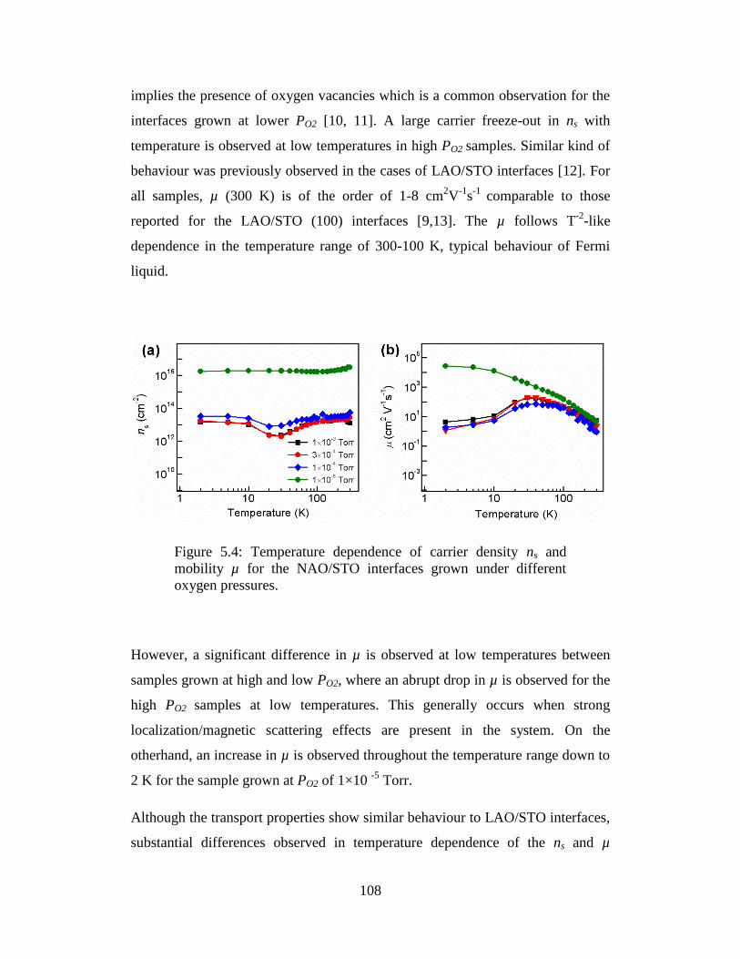
108
implies the presence of oxygen vacancies which is a common observation for the
interfaces grown at lower PO2 [10, 11]. A large carrier freeze-out in ns with
temperature is observed at low temperatures in high PO2 samples. Similar kind of
behaviour was previously observed in the cases of LAO/STO interfaces [12]. For
all samples, µ (300 K) is of the order of 1-8 cm2V
-1s
-1 comparable to those
reported for the LAO/STO (100) interfaces [9,13]. The µ follows T-2
-like
dependence in the temperature range of 300-100 K, typical behaviour of Fermi
liquid.
Figure 5.4: Temperature dependence of carrier density ns and
mobility µ for the NAO/STO interfaces grown under different
oxygen pressures.
However, a significant difference in µ is observed at low temperatures between
samples grown at high and low PO2, where an abrupt drop in µ is observed for the
high PO2 samples at low temperatures. This generally occurs when strong
localization/magnetic scattering effects are present in the system. On the
otherhand, an increase in µ is observed throughout the temperature range down to
2 K for the sample grown at PO2 of 1×10 -5
Torr.
Although the transport properties show similar behaviour to LAO/STO interfaces,
substantial differences observed in temperature dependence of the ns and µ
109
indicate the effect of the different polar layers. To further elucidate the polar layer
effects, a comparison study was carried out. For this, samples with LaAlO3,
PrAlO3 and NdGaO3 as the polar over layers were grown on STO. For the best
comparison all the samples were grown at same thicknesses of 10 uc and under
identical growth process (PO2 of 1×10 -3
Torr).
5.4. Comparison of various polar/non polar oxide interfaces
Figure 5.5a shows the temperature dependence of Rs for various polar/non-polar
oxide interfaces. Similar to the case of NAO/STO, PAO/STO interfaces also show
upturn in Rs at low temperatures. On the other hand, interestingly, LAO/STO and
NGO/STO interfaces show a typical metallic behaviour without appreciable
upturns in Rs. Further, their Rs at 300 K appears to have a strong dependence on
the RE cation of the polar layer, where Rs is larger (90 KΩ) for NAO compared to
that of LAO (20 KΩ). Figure 5.5b shows the ns variation with temperature;
LAO/STO and NGO/STO interfaces show minute carrier freeze-out towards low
temperatures compared to NAO/STO and PAO/STO, indicating that the interfaces
with LAO and NGO have less contribution from activated carriers. However, a
carrier recovery below 15 K is observed for the NAO/STO and PAO/STO
interfaces, which is possibly due to the difference transport mechanism in this low
temperature localized regime. The most remarkable effects are seen in
temperature dependence of mobility that is shown in figure 5.5c. For the
NAO/STO and PAO/STO interfaces, µ increases initially with decreasing
temperature and then drops dramatically for temperatures below 40 K.

110
Figure 5.5: Temperature dependence of sheet resistance, Rs, carrier
density, ns, and mobility, µ, for various combinations of polar/non-
polar oxide interfaces.
On the other hand, interfaces with LAO and NGO show an increase in µ and tend
to saturate at low temperatures. An interesting observation is that even though the
ns (2 K) is nearly the same (~2×10¹³
cm-2
) for all the interfaces, Rs and µ exhibit
significant divergence, implying a significant influence of the type of polar layer
on the charge carriers at the polar/non-polar interface. The possible effects of the
polar layers are discussed below.
5.5. Electronic correlation and strain effects
Although these polar layers seem to be similar in nature, yet there are few
differences. Firstly, these polar layers comprise of different chemical elements at

111
A-site (RE cation) and B-site in the perovskite (ABO3) structure. When the polar
layer (REBO3) is deposited on top of the TiO2 terminated SrTiO3 (100), the first
unit cell at the interface on either side can be viewed as a stack of REO/ TiO2 /SrO
layers. In this picture, across the interface, the TiO2 layer will have a different
electronic environment in the presence of different RE cations. Secondly,
different polar layers cause different lattice mismatch with STO, which in turns
create a different interfacial strain. To further understand these effects, the A-site
cationic dependence of the ns is plotted for corresponding interfaces as shown in
figure 5.6.
Figure 5.6: Variation in carrier density with Rare Earth (RE)
cations at the various polar/non-polar oxide interfaces.
Clearly ns (300 K) are higher in the case of La based interface and lower for Nd
based interfaces, similar to the case of SrTiO3/REO/SrTiO3 heterostructures
reported by Jang et al. [14]. There it is further shown that the electronic ground
state (metallic/insulating) can be controlled by RE cation at the interface and is
attributed to the electronic correlations of RE cation to the top STO layer which is
Nd Pr La
1
10
ns (c
m-2)
x 1
013
REAlO3 (300 K)
REGaO3 (300 K)
REAlO3 (2 K)
REGaO3 (2 K)
RE cation

112
further supported by theoretical calculations. However, in our case here, ns at 2 K
have rather small dependency on the RE cation with ns is of the order of 1-2 ×10¹³
cm-2
for all interfaces. The RE cation dependency of ns shown here further
suggests the electronic effects arising from polar layer control the charge
distribution at the interface.
Now getting back to the mobility case, referring to figure 5.5c, the µ drop was
only observed in the case of NAO/STO and not in the NGO/STO (Nd is A-site
cation for both cases), implying that we cannot attribute this µ drop to the
proximity effects of RE ions at the interface. So the only other difference these
polar layers offer is the lattice mismatch at the interface with the STO substrate. A
schematic diagram is shown in figure 5.7.
Figure 5.7: Schematic diagram showing the lattice constants of
polar oxides and SrTiO3.
Lattice mismatch here is estimated by considering in-plane lattice parameters.
Among them the NGO/ STO interface offers the least lattice mismatch (1.6%) and
NAO/STO the largest (3.6%).

113
Figure 5.8: (a) Mobility µ and (b) Carrier activation energy as a
function of the lattice mismatch at polar/non-polar oxides.
Figure 5.8a shows the µ variation with lattice mismatch; µ (300 K) shows modest
dependency to the lattice mismatch with values typically of the order of 1-5
cm2V
-1s
-1, which suggests the predominant electron-phonon scattering at 300 K.
In contrast, µ (2 K) shows strong dependence on lattice mismatch: µ is 500 cm2V
-
1s
-1 for NGO/STO and only 4 cm
2V
-1s
-1 for NAO/STO (a drop of a factor of 100).
It appears that the large lattice mismatch is limiting the µ. Recent reports on
LAO/STO interface using HRTEM [15] and HRXRD [16] showed that in the top
layers of the STO the Ti octahedra are distorted, strongly implying that the top
few layers of STO are under the influence of strain provided by the polar over
layers through structural coupling across interface. The fundamental issue here is
that the charge carriers occupy Ti sites and predominantly reside in the top few
layers of STO. The various polar layers offer a range of degree of distortions to
the top layers of STO due to the lattice mismatch, therefore the degree of strain/
distortions in these STO layers can be expected to play a crucial role in
manipulating the electronic properties at the interface. Consequently, the mobility
variation observed here can be ascribed to the degree of strain induced in STO
layers by lattice mismatch. Further we note that eventhough the carrier density ns
at 2 K is almost the same (2×10¹³
cm-2
) for all interfaces a large variation in µ is
observed, suggesting that e-e interactions play a key role in these various
114
interfaces. However the degree of disorder induced by strain may have an
influence to an extent. Thus, we interpret that the combined effects of strain and
electron correlations are crucial in controlling the µ. Further, because of a smaller
lattice mismatch a higher µ is expected in the case of NGO/STO (1.6%) compared
to the case of LAO/STO (2.3%) due to lesser mismatch, however the mobility
values are just comparable in both cases. This is attributed to the residual impurity
scattering in STO itself. We note that the strain values are estimated by
considering the lattice parameters at room temperature for STO and various polar
layers. The thermal expansion coeficient for STO and LAO are about 10-5
K-1
that
changes the lattice constants of individual layer by 0.4%. Therefore the variation
in strain would be less than that. Further, STO undergoes a cubic to tetragonal
phase transition at about 110 K.
As mentioned earlier a large carrier freeze out is observed in a certain temperature
range. To examine this, the activation energy is extracted from Arrhenius plots
(between 20 and 300 K) of the ns versus temperature graphs in figure 5.5b.
Activation energies of the order of few meV are in agreement with the previous
report on LAO/ STO [13]. Figure 5.8b shows activation energy as a function of
lattice mismatch. Interestingly, activation energy gradually increases with lattice
mismatch and it is largest (16 meV) for the NAO/STO. In general, the activation
energy indicates the relative position of carrier donor level from the conduction
band in energy scale. Its variation with lattice mismatch may suggest a relative
shift in position of donor level. Recently, it has been proposed that strain could
lead to distortion of Ti octahedra through octahedral rotation/tilt in STO based
heterostructures [14, 15], which in turn could alter the position of energy levels.
Since electronic effects are quite sensitive to the degree of octahedral distortions,
it is interesting to study the effects of octahedral distortions on novel phases at
these interfaces.
The above presented data established that the polar over layers play a key role in
governing the interface properties. The Rare earth cation at A-site is shown to
influence the carrier density at the interface, and the interface strain offered by

115
these various polar over layers is shown to control mobility at the interface. From
the above section, there is an indication that the 2DEG at various polar/non-polar
oxide interfaces exhibit a stronger localization of 2DEG compared to that at the
LAO/STO interfaces. The basic difference between NAO/STO and LAO/STO
interfaces is that the former one offers larger lattice mismatch of 3.6%. Stronger
localization can possibly give rise to different transport properties, and thus its
dependence on the NAO over layer thickness is very crucial to be investigated.
With this objective, the samples of NAO/STO interfaces with different thickness
of NAO were prepared. The transport properties of the corresponding samples are
discussed below.
5.6. Thickness dependence study of the NdAlO3/SrTiO3 interfaces
One of the characteristic features of the 2DEG at the LAO/STO system is the
thickness dependence of the insulator-metal transition with a critical thickness of
~ 4 uc of the LAO [17]. Furthermore, in the conventional LAO/STO case, a weak
to strong localization [18, 19] and magnetic Kondo behaviour [8] were reported in
thicker samples, suggesting that a variety of conduction mechanisms were
operating at these interfaces. Moreover superconductivity at these interfaces was
also shown to be sensitive to the thickness of the over layer where localization is
suggested to be minimum when superconductivity is observed [20]. In order to
investigate the NAO over layer thickness effects on transport properties, samples
with thicknesses ranging from 1-14 uc were grown. All these samples were grown
under identical conditions of oxygen pressure of 1x10⁻³
Torr, with energy density
of 1.3-1.4 Jcm-2
, and with a pulse repetition rate of 1 Hz. During the film growth,
the thickness of the NAO is monitored by RHEED. Conductivity for the
NAO/STO interfaces as a function of the number of unit cells of NAO is depicted
in figure 5.9. The samples show a clear transition from insulating to metallic state
at a thickness around 4 uc, with a change in the conductivity of more than three
orders of magnitude across the insulator to metal transition.
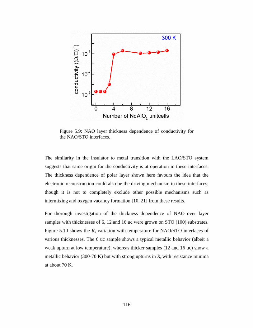
116
Figure 5.9: NAO layer thickness dependence of conductivity for
the NAO/STO interfaces.
The similarity in the insulator to metal transition with the LAO/STO system
suggests that same origin for the conductivity is at operation in these interfaces.
The thickness dependence of polar layer shown here favours the idea that the
electronic reconstruction could also be the driving mechanism in these interfaces;
though it is not to completely exclude other possible mechanisms such as
intermixing and oxygen vacancy formation [10, 21] from these results.
For thorough investigation of the thickness dependence of NAO over layer
samples with thicknesses of 6, 12 and 16 uc were grown on STO (100) substrates.
Figure 5.10 shows the Rs variation with temperature for NAO/STO interfaces of
various thicknesses. The 6 uc sample shows a typical metallic behavior (albeit a
weak upturn at low temperature), whereas thicker samples (12 and 16 uc) show a
metallic behavior (300-70 K) but with strong upturns in Rs with resistance minima
at about 70 K.

117
Figure 5.10: Temperature dependence of sheet resistance, Rs for the
NAO/STO interfaces with different NAO thicknesses (6, 12, and
16 uc).
The emergence of the upturns with over layer thickness observed here is in
agreement with previous reports on LAO/STO though the critical thickness for
the LAO/STO samples is about 15 uc [9]. However, a significant observation can
be made for the low temperature transport for the thicker NAO/STO samples, i.e.
below 15 K the variation in Rs is more distinct indicating a different type of
transport mechanism operating at low temperatures. Figure 5.11a and 5.11b show
the temperature dependence of ns and µ, respectively, for the corresponding
samples. For the thicker samples, ns decreases in the temperature range of 300-20
K, and this can be attributed to the localization of activated charge carriers at the
interface.

118
Figure 5.11: Temperature dependence of carrier density ns and
mobility µ for the NAO/STO interfaces with different NAO
thicknesses (6, 12, and 16 uc).
ns in this range can be fit with a simple Arrhenius equation of the form Ae -Ea/T
,
where Ea is the thermal activation energy for the activated charge carriers. The Ea
is of the order of 12 meV which is larger compared to 6 meV for the LAO/STO
interfaces [13]. As discussed in the previous section the large activation and
strong localization observed in thicker samples could be due to the large structural
distortions present in these systems arising from the larger interface strain.
Further, there is an increase in ns at low temperatures below 20 K down to 2 K,
simultaneously where an increase in Rs is observed. For temperatures below 20 K
the increase in both the Rs and ns implies that the transport mechanism cannot
only be simple band (Drude) conduction and indicates that other type of transport
mechanism is in operation at low temperatures. Contrary to this, for the 6 uc
sample there is no such carrier activation for ns with temperature. µ for the 6 uc
sample increases monotonically from 9 cm2V
-1s
-1at 300 K to 900 cm
2V
-1s
-1 at 2 K.
The relatively high mobility of the 6 uc sample would be favourable for studies of
superconductivity. On the other hand, for the thicker samples (12 and 16 uc) the µ
at 300 K is about 5 cm2V
-1s
-1, and it drops significantly at the low temperatures,
which gives further evidence for strong localization in these samples. The low
temperature behavior of Rs, ns and µ confirms the strong localization of carriers
associated with a change of transport mechanism at low temperatures. In general,
1 10 100
1011
1012
1013
1014
1015
1 10 100
10-2
100
102
104
Temperature (K)
ns (
cm
-2)
(b)
Temperature (K)
(a)
6 uc
12 uc
16 uc
(
cm
2 V
-1s
-1)

119
the observed low temperature sharp upturns in Rs can arise from various transport
mechanisms namely, variable range hopping (VRH) due to strong localizations, a
magnetic Kondo scattering and thermal activation. In order to further verify the
transport mechanism in our system, the low temperature variation of Rs is
analyzed.
The upturns in Rs could originate from magnetic Kondo effect following the
dependence given by R (T) =R0 ln (T/Tef). However this dependence does not fit
our data, indicating that Kondo scattering is not the governing mechanism here.
Moreover the non saturating trend of Rs even down to 2 K also further confirms
this. For the thicker samples the ns at 20 K are of the order of ~1012
cm-2
which is
one order of magnitude lower than that in the thin 6 uc sample. Hence, it seems
that there could be a critical ns at these interfaces below which the transport
mechanism converts to VRH in the strong localization regime. The reduced ns
seen in thicker samples could be due to the large amount of interface strain
created by thicker NAO over layers.
5.7. Strong localizations and variable range hopping transport
The observed strong localizations in 2DEG at the interface suggests that the most
likely mechanism would be VRH, which is a transport mechanism in which the
conduction takes place through hopping of carriers between localized states. The
variation of resistance in the VRH regime can be described by the equation
Here n is the dimensionality of the system [22]. Figure 5.12 shows the
corresponding 2D VRH (n = 2) fit for the experimental data at low temperatures
(40-2 K).

120
Figure 5.12: The ln (Rs) vs. (1/T)1/3
graph for 12 and 16 uc
NAO/STO samples, and a 2D variable range hopping (VRH) fit to
the experimental data in the temperature range of 2-20 K.
As evidenced from the figure 5.12 the experimental data below 15 K fits well the
VRH formula and significantly the T-1/3
dependence (n = 2) confirms the 2D
nature of the conducting channel. The crossover regime between the metallic and
VRH (70-20 K) follows a logarithmic dependence of temperature which may
indicate a weak localization regime for the electrons.
The VRH transport mechanism can be further evaluated by magneto transport
measurements, since in the hopping transport the carrier conduction is quite
sensitive to magnetic fields. Magneto-resistance (MR) measurements were
performed on the 12 uc NAO/STO sample at various temperatures with different
current (I) to magnetic field (B = µ0H) orientations. Figure 5.13 shows the out of
plane MR (magnetic field is perpendicular to the current and sample surface)
measured at various temperatures. The MR is negative at 2 K with -30 % at 9 T.
The negative MR is indeed one of the strong signatures for VRH type transport
[23, 24, 25]. Further, the negative MR diminishes with increase in temperature
and turns to positive MR for higher temperatures. The negative MR reaches a
minimum at about 20 K which is exactly the temperature range where the changes
0.3 0.4 0.5 0.6 0.7 0.8
8
10
12
14
16 12 uc
16 uc
ln (
Rs )
(1/T)1/3

121
in trend are simultaneously seen in Rs and ns. The origin of negative MR in VRH
is attributed to the disruption of the interference effects between forward
scattering events in the presence of magnetic field.
Figure 5.13: (a) Out-of-plane MR measured at different
temperatures for 12 uc NAO/STO sample. Inset: scaling of MR at
9 T with temperature for negative MR part. (b) MR (out of plane)
measured at 2 K with magnetic field showing linear variation at
high magnetic fields and Inset: a B2 dependence at low magnetic
fields.
By considering the interference among the hopping paths between two sites at a
distance RM apart, where RM is the optimum hopping length, it is shown that
interference affects the hopping probability between these two sites. Inset of
figure 5.13a shows the temperature dependence of MR in the negative MR regime
at 9 T which scales approximately to T-1
as expected in the case of 2D VRH [26].

122
The temperature dependence of hopping length (RM) basically determines the MR
dependence on temperature. Further, the positive MR observed above 20 K arises
from Lorentz scattering of electrons in presence of magnetic field, which has been
extensively studied for 2DEG at the LAO/STO interface [18, 27, 28]. Figure
5.13b shows the plot of MR as a function of magnetic field, with linear B
dependence at high magnetic fields and B2-dependence for low fields (shown in
inset of figure 5.13b), which is in accordance with theory and experiments in
VRH regime [26, 29]. To exclude the orbital contributions to MR in VRH regime,
measurements were further performed in in-plane mode (current and magnetic
field are parallel and in the plane of the 2DEG) which is shown in figure 5.14.
Figure 5.14: In-plane MR measured at different temperatures for
12 uc NAO/STO sample.
In this case, it can be seen that MR is negative for the temperatures below 20 K
and diminishes and turns to zero for the temperatures above 20 K. The absence of
MR above 20 K suggests the absence of Lorentz scattering of electrons in this in-
plane geometry. Figure 5.15 shows the angle dependence of Rs measured at 2 K
and 9 T. Here 0 degree corresponds to in plane mode and 90 degree corresponds
to out of-plane mode. It can be observed that the Rs show large anisotropy
between in-plane and out of-plane modes, which is due to the confinement effect

123
of the 2DEG. These MR measurements further confirm that the transport
mechanism at low temperatures for the thicker samples is governed by VRH and
this VRH regime begins to appear for below 20 K which is evidenced by the
change in the MR (from positive to negative).
Figure 5.15: Angle dependence of Rs at 2 K and 9 T with angle
between magnetic field to current changed from in-plane to out of
plane).
Generally, the hopping transport favours over other mechanisms when a
considerable amount of carrier localization is present in the system, the carrier
confinement would also be crucial in these 2D systems where the absence of
lateral transport can further favours the hopping transport. Finally, we comment
on the unusual carrier density recovery at low temperatures. The coincidence of
the critical temperature with the evolution of VRH regime, where the carrier
density increases as the temperature decreases suggests that it may relate to
hopping transport. Thus we suggest that the overall carrier density behaviour
could be understood by considering two regimes of transport mechanisms; a
0 90 180 270
0.98
0.99
1.00
Angle ()
Rs(
) / R
s(
)
124
regular transport in conduction band via extended states, thermally activated
charge carriers where the carrier density decreases with decreasing temperature.
We suggest that the lowest lying states are related to strongly localized states with
negligible hopping probability to other states. As more and more carriers freeze
into localized states, Coloumb interaction between localized states may mobilize
initially immobile electrons in this hopping transport regime, thus enhances the
mobile carrier density. The other possibility is the change in band fillings at this
low temperature regime where heavy bands with high electron density participate
in the conduction.
5.8. Summary
In this chapter the observation of 2DEG at new combinations of various
polar/non-polar oxides interfaces namely, NdAlO3/ SrTiO3, PrAlO3/SrTiO3 and
NdGaO3/ SrTiO3 is demonstrated. This study certainly provides a new insight in
in preparing various oxide interfaces with tunable properties at these polar/non-
polar oxide combinations. A detailed transport analysis revealed that the
properties of the 2DEG can be influenced by the polar over layers. This study
indicates that the combined effects of interface strain and electron correlations
offered by polar layers are crucial in these oxide interfaces. The lattice mismatch
of polar layers to the STO can induce large octahedral distortions in STO and the
observed variation in activation energy for carriers in these various polar/non-
polar layers could be an indication of such octahedral distortions in STO at the
interface. Even though naive thinking suggests is that bulk substrates expected to
induce the strain in over layers, however this study shows that at the interface the
substrate layers are also influenced by the over layers to an extent that can
influence the interface physics and properties. The observations such as rare earth
(RE) cation dependence of carrier density, lattice mismatch effects on mobility
offered by polar layers may provide an opportunity to tune the properties at
selected polar/non-polar oxide interfaces. Further, the observed thickness
dependence of metal-insulator transition for the NAO/STO interfaces suggests
that polar discontinuity may possibly be the prime origin of conductivity at these

125
polar/non-polar interfaces. Thickness dependence of localization effects of 2DEG
are observed at the NAO/STO interfaces. In the strong localized regime the
transport is governed by the VRH. These results further emphasize the dominant
role of over layer thickness in controlling the transport properties of 2DEG at
these interfaces through interface strain. Moreover the study presented in this
report can certainly assist to distinguish the localization from other mechanisms
which is very important in understanding the physics of electron transports in two
dimensional oxide systems.

126
References
[1] C. Cen, S. Thiel, G. Hammerl, C. W. Schneider, K. E. Andersen, C. S.
Hellberg, J. Mannhart, and J. Levy, “Nanoscale control of an interfacial
metal–insulator transition at room temperature,” Nature Materials, 7, 298-302
(2008).
[2] Y. Xie, Y. Hikita, C. Bell, and H. Y. Hwang, “Control of electronic
conduction at an oxide heterointerface using surface polar adsorbates,” Nature
communications, 2,494 (2011).
[3] C. W. Bark, D. A. Felker, Y. Wang, Y. Zhang, H. W. Jang, C. M. Folkman, J.
W. Park, S. H. Baek, H. Zhou, D. D. Fong, X. Q. Pan, E. Y. Tsymbal, M. S.
Rzchowski, and C. B. Eom “Tailoring a two-dimensional electron gas at the
LaAlO3/SrTiO3 (001) interface by epitaxial strain,” Proceedings of the
National Academy of Sciences, 108, 4720-4724, (2011).
[4] C. Cancellieri, D. Fontaine, S. Gariglio, N. Reyren, A. D. Caviglia, A.
Feˆte, S. J. Leake, S. A. Pauli, P. R. Willmott, M. Stengel, Ph. Ghosez, and
J.-M. Triscone, “Electrostriction at the LaAlO3/SrTiO3 interface,” Phys. Rev.
Lett. 107, 056102 (2011).
[5] C. W. Bark, P. Sharma, Y. Wang, S.H. Baek, S. Lee, S. Ryu, C. M. Folkman,
T. R.Paudel, A. Kumar, S.V. Kalinin, A. Sokolov, E. Y. Tsymbal, M. S.
Rzchowski, A.Gruverman, C.B. Eom, “Switchable Induced Polarization in
LaAlO3/SrTiO3 heterostructures,” Nano Letters, 12, 1765-1771 (2012).
[6] P. Perna, D. Maccariello, M. Radovic, U. Scotti di Uccio, I. Pallecchi, M.
Codda, D. Marré, C. Cantoni, J. Gazquez, M. Varela, S. J. Pennycook, and F.
Miletto Granozio, “Conducting interfaces between band insulating oxides:
The LaGaO3/SrTiO3 hetero-structure,” Applied Physics Letters, 97, 152111
(2010).
[7] N. Nakagawa, H. Y. Hwang, and D. A. Muller, “Why some interfaces cannot
be sharp,” Nature Materials, 5, 204-209 (2006).

127
[8] A. Brinkman, M. Huijben, M. Van Zalk, J. Huijben, U. Zeitler, J. C. Maan, W.
G. Van Der Wiel, G. Rijnders, D. H. A. Blank, and H. Hilgenkamp,
“Magnetic effects at the interface between non magnetic oxides,” Nature
Materials, 6, 493-496 (2007).
[9] C. Bell, S. Harashima, Y. Hikita, and H. Y. Hwang, “Thickness dependence
of the mobility at the LaAlO3/SrTiO3 interface,” Applied Physics Letters, 94,
222111 (2009).
[10] W. Siemons, G. Koster, H. Yamamoto, W. A. Harrison, G. Lucovsky, T. H.
Geballe, D. H. A. Blank, and M. R. Beasley, “Origin of charge density at
LaAlO3 on SrTiO3 hetero- interfaces: possibility of intrinsic doping,” Physical
Review Letters, 98, 196802 (2007).
[11] A. Kalabukhov, R. Gunnarsson, J. Borjesson, E. Olsson, T. Claeson, and D.
Winkler, “Effect of oxygen vacancies in the SrTiO3 on the electrical
properties of the LaAlO3/SrTiO3 interface,” Physical Review B, 75, 121404(R)
(2007).
[12] M. Huijben, G. Koster, H.J.A. Molegraaf, M.K. Kruize, S. Wenderich, J.E.
Kleibeuker, A. McCollam, V.K. Guduru, A. Brinkman, H. Hilgenkamp, U.
Zeitler, J.C. Maan, D.H.A. Blank, G. Rijnders. “High mobility interface
electron gas by defect scavenging in a modulation doped oxide
heterostructure,” arXiv: 1008.1896v1.
[13] M. Huijben, G. Rijinders, D. H. A. Blank, S. Bals, S. V. Aert, J. Verbeeck, G.
V. Tendeloo, A. Brinkman, and H. Hilgenkamp, “Electronically coupled
complementary interfaces between perovskite band insulators,” Nature
Materials, 5, 556 (2006).
[14] H. W. Jang, D. A. Felker, C. W. Bark, Y. Wang, M. K. Niranjan, C. T.
Nelson, Y. Zhang, D. Su, C. M. Folkman, S. H. Baek, S. Lee, K. Janicka, Y.
Zhu, X. Q. Pan, D. D. Fong, E. Y. Tsymbal, M. S. Rzchowski, C. B. Eom,
“Metallic and insulating oxide interfaces controlled by electronic
correlations,” Science, 331, 886 (2011).

128
[15] C. L. Jia, S. B. Mi, M. Faley, U. Poppe, J. Schubert, and K. Urban, “Oxygen
octahedron reconstruction in the SrTiO3/LaAlO3 heterointerfaces investigated
using aberration-corrected ultrahigh-resolution transmission electron
microscopy,” Physical Review B, 79, 081405(R) (2009).
[16] J. E. Boschker, C. Folkman, C. W. Bark, A. F. Monsen, E. Folven, J. K.
Grepstad, E. Wahlstrom, C. B. Eom, and T. Tybell. “Structural coupling
across the LaAlO3 /SrTiO3 -interface: High-resolution x-ray diffraction study,”
Physical Review B, 84, 205418 (2011).
[17] S. Thiel, G. Hammerl, A. Schmehl, C. W. Schneider and J. Mannhart,
“Tunable quasi-two-dimensional electron gases in oxide heterostructures,”
Science, 313, 1942 (2006).
[18] F. J. Wong, R. V. Chopdekar, and Y. Suzuki, “Disorder and localization at
the LaAlO3/ -SrTiO3 interface,” Physical Review B, 82, 165413 (2010).
[19] T. Hernandez, C. W. Bark, D. A. Felker, C. B. Eom, and M. S. Rzchowski,
“Localization of two-dimensional electron gas in LaAlO3/-
SrTiO3 heterostructures,” Physical Review B, 85, 161407 (R) (2012).
[20] N. Reyren, S. Thiel, A. D. Caviglia, L. Fitting Kourkoutis, G. Hammerl, C.
Richter, C. W. Schneider, T. Kopp, A. -S. Ruetschi, D. Jaccard, M. Gabay, D.
A. Muller, J. -M. Triscone, and J. Mannhart, “Superconducting interfaces
between insulating oxides,” Science, 317, 1196-1199 (2007).
[21] P. R. Wilmott, S. A. Pauli, R. Herger, C. M. Schlepu¨tz, D. Martoccia, B. D.
Patterson, B. Delley, R. Clarke, D. Kumah, C. Coinca, and Y. Yacoby,
“Structural basis for the conducting interface between LaAlO3 and SrTiO3,”
Physical Review Letters, 99, 155502 (2007).
[22] N. F. Mott, “Conduction in glasses containing transition metal ions,” J. Non-
Crystal. Solids, 1, 1 (1968).
[23] V. I. Nguyen, B. Z. Spivak and B. I. Shklovskii, “Aharonov-Bohm
oscillations with normal and superconductive flux-quanta in hopping

129
conduction,” Pis'ma Zh. Eksp. Teor. Fiz. 41, 35 (1985) - English translation:
Sov. Phys. JETP Letters, 41, 42 (1985).
[24] V. I. Nguyen, B. Z. Spivak and B. I. Shklovskii, “Tunnel hops in disordered
systems,” Zh. Eksp. Teor. Fiz. 89, 1770 (1985) - English translation: Sov.
Phys. JETP 62, 1021 (1985).
[25] U. Sivan, O. Entin-Wohlman, and Y. Imry, “Orbital magnetoconductance in
the variable-range–hopping regime,” Physical Review Letters, 60, 1566
(1988).
[26] W. Schirmacher, “Quantum-interference magnetoconductivity in the variable-
range-hopping regime,” Physical Review B, 41, 2461 (1990).
[27] X. Wang, W. M. Lü, A. Annadi, Z. Q. Liu, K. Gopinadhan, S. Dhar, T.
Venkatesan, and Ariando, “Magnetoresistance of two-dimensional and three-
dimensional electron gas in LaAlO3/SrTiO3 heterostructures: Influence of
magnetic ordering, interface scattering, and dimensionality,” Physical Review
B, 84, 075312 (2011).
[28] M. Ben Shalom, C. W. Tai, Y. Lereah, M. Sachs, E. Levy, D. Rakhmilevitch,
A. Palevski, and Y. Dagan, “Anisotropic magnetotransport at the
SrTiO3/LaAlO3 interface,” Physical Review B, 80, 140403(R) (2009).
[29] K. Schlenga, H. Bach and K. Westerholt. “Magnetoresistance of
La2−xBaxCuO4−δ single crystals with concentrations close to the metal-
insulator transition,” Physica C, 221, 161 (1994).

130

131
Chapter 6
Anisotropic two dimensional electron gas at the
LaAlO3/SrTiO3 (110) interface
Abstract
So far the emergent phenomena in LAO/STO based systems were studied
specifically only at the interfaces constructed along the (100) crystallographic
orientation. The occurrence of conductivity is believed to be driven by
polarization discontinuity leading to an electronic reconstruction. In this scenario,
the crystal orientation plays an important role and no conductivity would be
expected, for example for the interface between LaAlO3 and (110)-oriented
SrTiO3, which should not have a polarization discontinuity. Here, it is
demonstrated that a high mobility two-dimensional electron gas (2DEG) can also
arise at the LAO/STO (110) interface. The (110) interface shows transport
properties and LaAlO3 layer critical thickness for the metal-to-insulator transition
similar to those of (100) interfaces, but with a strong anisotropic characteristic
along the two in-plane crystallographic directions. The anisotropic behaviour is
further found to be sensitive to the oxygen growth conditions where the ration of
resistance between two in-plane crystallographic directions shows dramatic
dependence. Density functional theory calculations reveal that electronic
reconstruction, and thus conductivity, is still possible at this (110) interface by
considering the energetically favourable (110) interface structure, i.e. buckled
TiO2/LaO, in which the polarization discontinuity is still present. Transmission
electron microscopy experiments reveal perfect growth of the interface and
indicate a further signature of possible buckling of the interface. An alternative
zig-zag/buckled interface model for (110) is proposed in place of planar interface.
The (110) interface further shows field effect characteristics with external electric
fields. The interface shows trans-conductance similar of a field effect transistor

132
with a significant anisotropy in mobility is observed along crystallographic
directions whereas the carrier density is isotropic.

133
6.1. Introduction
The conductivity of the crystalline LAO/STO (100) interface is mostly interpreted
to originate from electronic reconstruction which is a direct consequence of the
polarization discontinuity11
at the interface between the two oxides. The
electrostatic charge representation for the LAO/STO case is shown in figure 6.1.
Figure 6.1: Layout of the polar catastrophe model for
LaAlO3/SrTiO3 interface, on (a), (100) and (c), (110)-oriented STO
substrates, where planes are segmented as planar charge sheets. In
the case of (100), charge transfer is expected while in the case of
(110) there is no polarization discontinuity and hence no charge
transfer. (b) and (d), Atomic picture of the interfaces for
representations (a) and (c), respectively.
134
In this case, the ABO3 perovskite structure of the SrTiO3 (100) substrate can be
considered as stacks of (SrO)0
and (TiO2)0
as shown in figure 6.1a, whereas for
the LaAlO3 it consists of charged sheets of (LaO)+1
and (AlO2)-1
, which leads to a
polarization discontinuity at the interface between the LAO and STO. According
to the polarization discontinuity picture this catastrophe can be avoided by
transferring a net charge to the STO at the interface, thus the conductivity at the
interface [1]. The atomic representation of figure 6.1a is shown in figure 6.1b with
Ti (+3) formation at the interface where the electrons occupy the TiO2 plane at the
interface. On the other hand, for the case of LAO/STO interfaces prepared on
SrTiO3 (110) substrates as shown in figure 6.1c, both the STO and LAO can be
represented by planar stacks of (ABO)+4
and (O2)-4
layers as proposed in [2, 3],
which leads to no polarization discontinuity at the interface. The atomic
representation of figure 6.1c is shown in figure 6.1d constructed with parallel
planes of SrTiO and O2 planes and LaAlO and O2 planes, respectively. According
to the polar discontinuity picture consequently here no conductivity would be
expected for such LAO/STO (110) interfaces. However, no systematic
experimental investigation of interfaces with respect to the crystallography has
been carried out so far.
6.2. Growth and characterization of LaAlO3/SrTiO3 (110) thin films
The LAO/STO (110) interface samples were prepared with various LAO
thicknesses (N) from 1 to 14 unit cells (uc), and under different PO2 ranging from
5×10⁻⁵
to 5×10⁻³
Torr on atomically flat STO (110) substrates. The LAO films
were deposited from a single-crystal LAO target at 720 °C by pulsed laser
deposition. The laser (248 nm) energy density was 1.4 J/cm2 and repetition rate
was 1 Hz. During deposition, the film growth was monitored using in-situ
RHEED. After deposition, all samples were cooled to room temperature at 10
°C/min in oxygen at the deposition pressure. For comparison with the
conventional (100) case, LAO/STO (100) samples were grown with 12 uc LAO
layers under the same preparation conditions.

135
For the (100) case, substrates were treated with well-established conditions;
buffered HF for 30 sec followed by thermal annealing at 950 °C for 2 hours in air
[4, 5]. For the (110)-oriented STO, the substrates were annealed for 3 hours at
1050-1100 °C in air [6]. Figure 6.2a shows an atomic force microscopy (AFM)
topography image of the TiO2 terminated STO (100) substrate surface, with a step
height of 0.39 nm, which is the unit cell spacing in STO (100).
Figure 6.2: Atomic force microscopy (AFM) images of the STO
(100) and (110) substrates. Images of step flow surfaces of treated
(a) STO (100), and (b) STO (110) substrates. Inset in (b) is the
surface morphology of 12 uc LAO/STO (110) sample with visible
step flow.
Figure 6.2b shows an AFM image of a treated STO (110) substrate which clearly
shows well defined terraces, typically 150-200 nm wide. The step height in this
case is about 0.28 nm, which is the unit cell spacing along the [110] direction. The
most probable surface termination is expected to be Ti-rich TiO as reported earlier
[6]. The step edges appear to be facetted along the [001] and low index
crystallographic directions giving rise to the triangular shaped steps [7]. The inset
of figure 6.2b shows an AFM topography image after the growth of 12 unit cells

136
(uc) of LAO on STO (110). The preserved step flow surface clearly indicates
quality of the samples with layer by layer growth. Thicker LAO films of about 15
nm were grown to enable confirmation of the growth orientation of the LAO on
STO (110) substrates by x-ray diffraction (XRD). Figure 6.3 show the XRD
pattern obtained for the (15 nm) LAO/STO (110) film. From the figure it is
evident that LAO film grows coherently along the (110) direction.
Figure 6.3: XRD pattern for the thin film of (15 nm) LAO/STO
(110).
6.3 Electrical transport properties
Electrical characteristics for all the samples such as the sheet resistance, Rs,
charge density, ns, and Hall mobility, µ, were measured using Van der Pauw
geometry. Figure 6.4a shows Rs versus temperature for the LAO/STO (110)
samples grown at different oxygen partial pressures (PO2) with a fixed thickness
of 12 unitcells (uc) LAO. Strikingly, these interfaces show conductivity
reminiscent to the (100) case (figure 6.4b), albeit with a larger dispersion with
respect to the oxygen pressure during growth. The Rs follows a T2-like

137
dependence over a temperature range of 300-100 K and tends to saturate at low
temperatures.
Figure 6.4: Temperature dependence of the sheet resistance Rs (T)
of the LAO/STO interfaces, for different oxygen partial pressures
(PO2) during growth on (a), (110) and (b), (100)-oriented STO
substrates.
The samples grown at higher oxygen pressures show a resistance upturn at lower
temperatures, a typical localization/Kondo-behavior indicating the presence of
magnetic scattering centers at the interface. While Kondo scattering in the (100)
case is reported only for LAO thickness larger than 15 uc [8-10], in the case of
(110) it is seen even for 10 uc LAO thickness indicating stronger scattering
effects. We note here that for the (100) case the dispersion in the resistivity with
oxygen deposition pressures was also reported but for samples with “thicker”
LAO layers of 20 uc [8], implying different sensitivity to the LAO thickness
between these interfaces. Interestingly, there is a temperature shift in the
resistance-minimum with the oxygen growth pressure, indicating that the strength
of the scattering at the interface is sensitive to the deposition conditions. We note
here that resistivity measurements have been carried out down to 2 K, and it is
feasible that some of these samples may become superconducting at lower
temperatures.

138
Figure 6.5: (a) Carrier density ns and mobility µ variation with
temperature for LAO/STO (110) and (b) for LAO/STO (100)
samples grown at different PO2.
Carrier density and mobility for the samples were extracted from Hall
measurements and are summarized in figure 6.5. For the (110) samples (figure
6.5a), ns decreases with decreasing temperature, for the samples grown at higher
partial pressures ns at low temperature (2 K) tends towards a constant value of
about 1.5×10¹³
cm-2
, which is somewhat lower than the residual carrier density of
about 2.5×10¹³
cm-2
for the LAO/STO (100) samples (figure 6.5b). This could be
due to the preferred occupancy of the Ti-3d orbitals at the interface which may
localize some of the electrons [11, 12]. For the thermally activated charge carriers
in the (110)-samples we find activation energy of about 9 meV, whereas in
LAO/STO (100) interfaces activation energy of 6.0 meV has been reported [13].
For both orientations, the measured µ follows a power law temperature
dependence for T>100 K, as µ~5×10⁶T
−2.2. All the samples grown at higher
pressures show µ values of the order of 200–600 and 2–7 cm2V
-1s
-1 at 2 K and
300 K, respectively. These values correspond well with those reported in
literature for the LAO/STO (100) interfaces [9, 14]. We notice a decrease in the µ
in the (110)-case, simultaneous with Kondo features becoming visible in the Rs
(T) curves. For the (110) sample grown at 5×10⁻⁵
Torr, the ns at 300 K is 4.9×10¹⁴

139
cm-2
, which has the µ of 12,000 cm2V
-1s
-1 at 2 K, suggesting contribution from
other sources such as oxygen vacancies [14,15] and defect centers present near
the interface.
6.4 LaAlO3 thickness dependent insulator-metal transition
One of the characteristic features of the LAO/STO (100) interfaces, and
considered as one of the most important arguments for a polarization
discontinuity driven mechanism, is the dependence of the sheet conductivity on
the number of unit cells of LAO with the observation of an insulator to metal
transition at 3-4 uc of LAO layers [16].
To investigate the thickness dependence interface conductivity for the LAO/STO
(110) case, the conductivity versus the number of LAO unit cells N grown on the
STO (110) substrates is measured and is shown in figure 6.6. For the thickness
dependence case all samples were prepared at the same PO2 of 1×10⁻³
Torr. As
evident from the figure samples are insulating for low N (N < 3) and metallic state
at higher N (N ≥ 4) values. For the samples below 3 uc thickness the conductivity
is out of measurement limit of the instrument. All of the conducting samples (N ≥
4) show nearly equal conductivities. The 3 uc sample showed a slight higher
conductivity relative to 1 or 2 uc samples although it still behaves like an
insulator. Data points marked in figure 6.6 with open red circle are for a sample
initially having 3 uc of LAO (insulating state), followed by the growth of 2 more
uc making it 5 uc in total.

140
Figure 6.6: LaAlO3 thickness dependence of sheet conductivity.
The room temperature sheet conductivity as a function of number
of unit cells of LaAlO3 for the LAO/STO (110) samples, clearly
showing the insulator to metal transition at about 4 uc (data points
marked with open red circle are for a sample initially having 3 uc
of LaAlO3, followed by the growth of 2 more uc making it 5 uc in
total).
Strikingly, with the thickness of 5 uc, the sample then became metallic from
insulating state. The sample with N = 0 corresponds to STO (110) substrate which
kept under identical growth conditions as the LAO/STO (110) samples.This
treated substrate shows an insulating behavior ruling out the self-reduction of
STO (110) at high deposition temperatures and pressure as the origin for this
conductivity. The fact that there are some similarities between (110) and (100)
case, including the insulator to metal transition at around 4 uc of LAO, indicates
that a very similar mechanism is at work for the formation of the 2DEGs for both
(100) and (110) cases.
At the LAO/STO interfaces the 2DEG was presumed to be the result of a direct
manipulation of electronic reconstruction that promote electrons to the conduction
band of STO, which requires energy of the order of 3.2 eV. Recent experimental
work involving amorphous over layers on STO showing a conductive interface

141
has brought in the importance of interface chemistry [17]. Under this scenario
oxygen diffusion from STO surface during film growth was deemed responsible
for the interface conductivity. What was striking was the similarity of the results
between the amorphous and crystalline over layers in terms of the saturation in
charge density and conductivity with the film thickness. Unlike their crystalline
counterparts, however in the case of amorphous over layers, the carriers generated
by creation of oxygen vacancies show thermal instability and lose conductivity
when subjected to a 150 °C annealing step in air or oxygen atmosphere.
To check the role of oxygen vacancy scenario, we performed subsequent post
annealing steps on the as deposited samples. Samples were annealed in oxygen
environment at 500 oC for 2 hour and these crystalline LAO/STO (110) samples
preserve the conductivity similar to the conventional LAO/STO (100) samples.
However, annealed samples show a reduction in the carrier density from that of as
deposited samples. This observation of conductivity at LAO/STO (110) calls into
question the polarity issues in these complex oxides. Recently, Stengel et al. [18]
discussed the issue of polarity in various oxides, especially the case of LAO and
STO surfaces, where it is shown that in LAO case, the surface with cleavage
planes are shown to be energetically favorable than a simple polar (001) surface.
These observations suggest that polar oxides surfaces show a tendency to form
stable surfaces. In this scenario, the atomic structure of the interface would be
critical to determine polarity effects at this LAO/STO (110) heterostructures.
6.5 Density functional theory
First-principles density functional theory (DFT) calculations for LAO/STO (110)
interfaces were performed using the generalized-gradient approximation (GGA)
[19] and the projected augmented wave (PAW) method with a plane wave basis
set as implemented in the Vienna Ab initio Simulation Package (VASP) [20-22].
Density functional theory (DFT) calculations were performed on STO (110)
surfaces with various possible atomic surface terminations. Five different surface
terminations, i.e., TiO, Sr, O2, O, and SrTiO terminations were considered. The
schematic of the different possible terminations are shown in the figure 6.8.

142
The stability of these various possible terminations is further analyzed by energy
calculations. The results suggest that buckled TiO termination at STO (110)
surface is more favorable than a hypothetical polar stoichiometric SrTiO surface
consistant with earlier reports [23].
Figure 6.7: Schematic of the various possible terminations
considered for the STO (110). (a) TiO, (b) Sr, (c) O2, (d) O, (e)
SrTiO terminations. The calculations showed that the TiO
termination is the energetically most stable.
AFM results performed on STO (110) surface indicate the formation of good
surface termination (figure 6.2a). Various surface analysis techniques such as time
of flight measurements performed on annealed STO (110) revealed that the STO
(110) surfaces have Ti-rich termination [6]. The formation of this termination is
likely due to surface reconstruction processes. To investigate the possibility of
such reconstruction, a careful analysis of RHHED patterns is carried out on
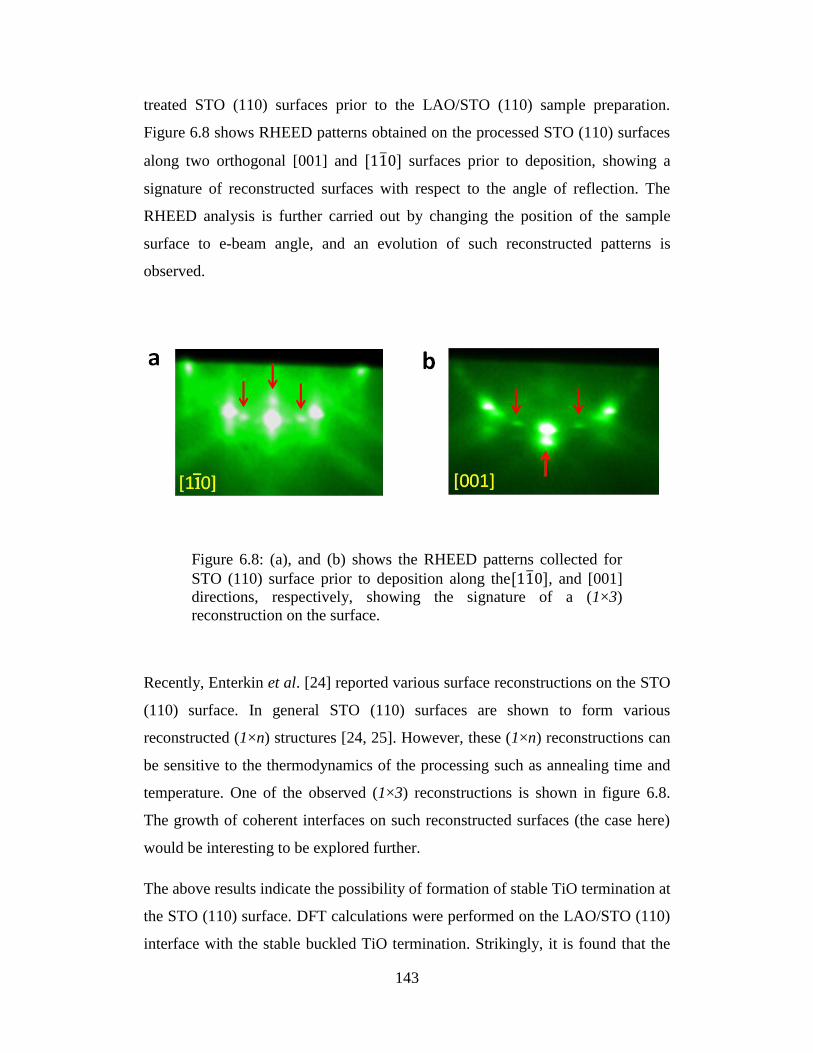
143
treated STO (110) surfaces prior to the LAO/STO (110) sample preparation.
Figure 6.8 shows RHEED patterns obtained on the processed STO (110) surfaces
along two orthogonal [001] and surfaces prior to deposition, showing a
signature of reconstructed surfaces with respect to the angle of reflection. The
RHEED analysis is further carried out by changing the position of the sample
surface to e-beam angle, and an evolution of such reconstructed patterns is
observed.
Figure 6.8: (a), and (b) shows the RHEED patterns collected for
STO (110) surface prior to deposition along the , and [001]
directions, respectively, showing the signature of a (1×3)
reconstruction on the surface.
Recently, Enterkin et al. [24] reported various surface reconstructions on the STO
(110) surface. In general STO (110) surfaces are shown to form various
reconstructed (1×n) structures [24, 25]. However, these (1×n) reconstructions can
be sensitive to the thermodynamics of the processing such as annealing time and
temperature. One of the observed (1×3) reconstructions is shown in figure 6.8.
The growth of coherent interfaces on such reconstructed surfaces (the case here)
would be interesting to be explored further.
The above results indicate the possibility of formation of stable TiO termination at
the STO (110) surface. DFT calculations were performed on the LAO/STO (110)
interface with the stable buckled TiO termination. Strikingly, it is found that the

144
origin for the unexpected conductivity in the (110) case can be explained by
considering energetically stable buckled TiO termination. The electronic
configuration of interfaces with such a buckled interface structure was modeled
by DFT as shown in figure 6.9a. To study the thickness dependence of LAO
monolayers deposited on STO (110) substrate, a slab model as shown in figure
6.9a is used.
Figure 6.9: Density functional theory calculations. (a) Schematic
cell structure of LAO/STO (110) interface with TiO terminated
STO (110). (b) The total density of states for different numbers N
of LAO monolayers deposited on STO (110), clearly shows the
band gap decrease with increasing N and an insulator to metal
transition occurring at 4 uc. (c) The partial density of states for O-
2p projected onto each layer for N=6 monolayers of LAO
deposited onto TiO terminated (110) STO.
To avoid the spurious intrinsic electronic field, inversion symmetry of the slab is
assumed to avoid spurious electronic field. In all calculations, a vacuum region of
12 Å between repeated slabs is taken. A kinetic energy cut off is set to be 400 eV
for the plane wave basis and the slab is sampled with 8×8×1 k-point grid in
combination with the tetrahedron method. While the in-plane lattice constant is
fixed at the relaxed lattice constant of bulk STO (a=3.944 Å), all coordinates of

145
atomic positions along the c-direction perpendicular to the interface are fully
relaxed until the forces become less than 0.01 eV/Å. The convergence of our
calculations was carefully checked. These calculations show that the energy gap
for bulk STO is about 1.8 eV separating the valence band with O-2p characters
and the conduction band mainly composed of Ti-3d.
For LAO, the obtained band gap is about 3.2 eV. These estimated values of the
band gap are similar to the ones previously reported by DFT calculations [26],
and are smaller than the ones observed experimentally. However, the
underestimating the energy gap within GGA is well known and the GGA+U
approach, for instance, gives an improved description. Indeed as shown in figure
6.9b, an insulator to metal transition with increasing number of LAO mono layers
is obtained. The critical thickness for insulator to metal transition is about 4 uc
which is in agreement with our experimental observation. This result shows that
by viewing the LaO/TiO2 as buckled layers, the thickness dependence of the
insulator to metal transition arising from avoiding the polarization catastrophe can
be reproduced [27].
Figure 6.9c shows the partial density of states for O-2p projected onto each layer.
From the figure we can see clearly that the top of the valence band moves toward
Fermi level as we approach the surface, suggesting that there can still exist
intrinsic electrostatic fields to avoid the polar catastrophe due to the polar
discontinuity caused by the buckled interface. This intrinsic electrostatic field can
induce the insulator-metal transition when this electrostatic potential exceeds the
band gap where the O-2p states cross over Ti 3d states and makes charge transfer.
In our case, this transition occurs at N < 4 as shown in figure 6.6. Note, however,
the critical value of N might depend on approximations used for calculations. We
find by performing GGA+U calculations that the main conclusion are
qualitatively the same. Thus, the density functional theory study reveals that the
interface between LaAlO3 and the energetically favorable atomic structure of the
TiO terminated SrTiO3 (110) can support the conductivity with the interface is
represented by an alternate way, namely, the buckled interface in which the
polarization discontinuity is still present.

146
6.6 Transmission electron microscopy of the (110) interface
To investigate the possibility of such proposed buckled atomic structure at the
(110) interfaces, we performed cross sectional scanning transmission electron
microscopy (STEM) on the LAO/STO (110) interfaces samples for STEM were
prepared using cutting, mechanical grinding, polishing and low voltage Ar ion
beam milling as a final polishing step. High angle annular dark field STEM
images were recorded using a FEI Titan 80-300 microscope with a corrector for
spherical aberration of the condenser lenses and a monochromator. The
microscope was operated at 300 kV. The electron beam is incident along the [001]
direction to the LAO/STO (110) interface.
Figure 6.10: High-angle annular dark-field scanning transmission
electron microscopy (TEM) images of the LAO film on the STO
(110) substrate shows an epitaxial growth of the LAO/STO (110)
heterostructure (A-site atoms La and Sr are indicated by red and
blue, respectively, and the B-site Al and Ti by orange and purple,
respectively). A magnified view of the elemental mapping across
the interface is also shown on the right side.

147
Figure 6.10 shows a high-angle annular dark-field (HAADF) STEM image of the
LAO film grown on the STO (110) substrate. The image shows a perfect epitaxial
growth of the LAO across the interface of the heterostructure along the (110)-
orientation. The signal from the atom columns depends on the atomic number
[28]. The ratio between the signals of the Al and La atom columns is expected to
be less than 10%. In addition, the projection along the Al atom columns also
includes O atoms further adding to the background signal of the Al columns. We
also note that the background intensity is generally higher in LAO compared to
the result of (100) interfaces [29].
Figure 6.11: Proposed atomic picture for LAO/STO interface on
(110)-oriented STO, considering the (110) planes of STO and LAO
as buckled sheets.
The Al and Ti (B-site) atom columns are visible in the STEM images. However, it
is found that it is difficult to use them as indicators of the interface between the
LAO and STO film on the basis of poor signal to background ratio. Therefore, the
La and Sr (A-site) atom columns have been used as indicators for the
film/substrate interface. In the figure 6.10, a higher resolution of elemental
mapping at the interface representing the arrangement of La (red) and Sr (blue)
positions in both LAO and STO is also shown. We notice some of the La and Sr
atoms at the interface extend up to 2-4 uc rather than 2 uc as anticipated. Both the
sparseness of such extended facets and the absence of connectivity among them
rule out other mechanisms for conduction (for example an effective (100)

148
interface at 45 degrees). However, the proposed buckled zig-zag model cannot be
distinguished just by identifying only the A-site cations as in our current STEM
data. Therefore, one needs to further resolve the chemical identity of the B-site
cations alongside A-site cations in order to confirm the proposed buckled
structure. Figure 6.11 show the models for the interfaces along (100) and (110)
interfaces. For (100) case the interface represented by a planar interface where the
Ti-O chain having a linear chain arrangement whereas a modified interface model
is proposed for (110) interface that is a zig-zag buckled interface.
6.7 Anisotropic conductivity at LaAlO3/SrTiO3 (110) interfaces
Considering all the data presented above, it is remarkable that, the (110)-samples
are not only conducting, but also bear remarkable similarities to the conductance
properties of the (100) case. However, it is noted that the STO (110) surface is
crystallographically anisotropic in terms of atomic arrangement. In most of the
transition metal oxide systems, the transition metal and oxygen bonding
arrangement is shown to be crucial in transport properties.
The STO (110) surface consists of two orthogonal directions [1 0] and [001]. In
the case of STO (110) the bonding of Ti-O along these two directions is different
as shown in figure 6.12c. Directional dependence transport measurements on
LAO/STO (110) samples were performed with respect to these crystallographic
directions and (figure 6.12). Crystallographic directions of the surface of STO
(110) identified as specified by the substrate supplier (Crystec GmbH). Strikingly,
along [1 0] direction (figure 6.12a) strong localization effects are seen at low
temperatures while along [001] (figure 6.12b) such localizations are absent. A
basic difference between these two directions is the presence of linear Ti-O-Ti
chains along [001] and buckled Ti-O-Ti chains along [1 0] as depicted
schematically in figure 6.12c.

149
Figure 6.12: Anisotropic conductivity of the LAO/STO (110)
interfaces. Rs (T) measured along (a), and (b), [001]
directions for the LAO/STO (110) samples grown at different
oxygen partial pressures. (c) Schematic view of The Ti chain
arrangement along the ] and [001] directions. (d) Deposition
oxygen pressure dependence of Rs at 2 K measured along the
and [001] directions.
The deposition pressure dependence of Rs at 2 K is plotted in figure 6.12b for both
directions. Clearly, the conductivity along the direction has a much
stronger dependence on deposition pressures compared to the [001] direction,
indicating the strong role of the Ti-O-Ti chain and their differences along the two
orthogonal directions. The growth pressure dependence may also suggest that the
defect chemistry along these two directions would be different. It is noted that the
sample deposited at PO2 of 5×10⁻⁵
Torr has a considerable oxygen vacancy
contribution which is also further showing a dramatic anisotropy along the

150
crystallographic directions, suggesting that the oxygen vacancy formation at
atomic level would be different along these two different directions.
In previous reports on LAO/STO (100) case, the anisotropy is investigated and it
is attributed to arise from a possible step edges [30] of the STO (100) substrate.
However, the magnitude of this anisotropy is small. It is also shown that there is
no systematic dependence of the step edges direction. In order to understand the
role of step edges, the anisotropy measurements were performed on LAO/STO
(100) samples also. Figure 6.13 shows directional dependence Rs versus
temperature, measured along [010] and [001] directions for the LAO/STO (100)
samples grown at different PO2. Unlike the case of LAO/STO (110) here a very
small anisotropy is observed in (100) case with respect to orthogonal [010] and
[001] directions. Since in (100) case the two directions are crystallographically
isotropic, thus this small anisotropy in (100) case could arise from step edge
scattering.
Figure 6.13: Directional dependence electrical transport in case of
LAO/STO (100) interfaces. Rs (T) measured along [010] (a), and
[001] (b), directions for the LAO/STO (100) samples grown at
different oxygen partial pressures.
.

151
It suggests that step edge scattering can give anisotropy in the system but it is
minimal when compared to intrinsic crystallographic anisotropy. The intrinsic
carrier localizations arises due to a degree of disorder in the system might also
result in anisotropy, but it cannot explain the anisotropy in the case of high
conducting sample of 5×10⁻⁵
Torr. Thus, the large anisotropy seen in (110) must
have an intrinsic origin related to the atomic arrangements of atoms, especially to
the Ti-O bonding. To quantify the exact magnitude of the intrinsic anisotropy one
need to perform nanoscopic transport measurements that can also exclude step
edge scattering effects.
6.8 Electric field effect on LaAlO3/SrTiO3 (110) interfaces
One of the characteristic features of the LAO/STO interfaces is the electric field
tuning of interface properties. Various types of electric field measurements were
performed. Sample of (5 uc) LAO/STO (110) grown at PO2 of 1×10⁻³
Torr is used
for the field effect study. Sample interfaces were accessed by directly wire-
bonding Al wires.
Figure 6.14: The voltage (V)-current (I) characteristics of the
sample along [001] direction at a temperature of 1.9 K.
-1.0 -0.5 0.0 0.5 1.0
-2
-1
0
1
2
50
V (
Vo
lt)
I (mA)
50
40
20
0
-20
-40
-50
VG (V)
-50

152
To apply back gate voltage bias, the source terminal was connected to the back
gate and the leakage current through the 0.5 mm thick STO substrate was
monitored through source current. Figure 6.14 show the current (Id)-voltage (Vds)
characteristics as a function of VG. The conductance of the interfaces is ohmic in
nature without any evidence of any tunneling characteristics as evident from the
linearity of the current-voltage. Figure 6.15 shows the VG dependence of the
resistance of the interface measures along two crystallographic directions showing
a considerable field effect. At positive gate bias applied to the interface the
resistance of 2DEG decreases, whereas for negative bias the resistance increases
more drastically. There appears a hysteresis behavior in the initial sweep of
voltages.
Figure 6.15: Sheet resistance of the LAO/STO (110) interface as a
function of back gate voltage in (a) and (b) [001] directions
measured at 1.9 K for 5 repeated measurements.
This hysteresis in the resistance is identified to be arising from the charge traps at
the interface and this can be diminished significantly by cycling the voltage as
shown in the figure. Therefore to go to the field effect ground state of the system,
the back gate voltage was swept five times at 1.9 K before the start of each
measurement which reduces the hysteresis considerably and also monitors the
reproducibility of the results. To investigate the anisotropy behavior that is shown
in figure 6.12, properties such as resistance, carrier density and mobility were

153
investigated with the gate electric field. Figure 6.16a shows the transfer
characteristics (source-drain current Id vs. back gate voltage VG) of the interface
as a function of source voltage Vds at a temperature of 1.9 K in [001] direction.
Figure 6.16: Drain current (Ids) vs back gate voltage (VG) as a
function of source-drain voltage (Vds) along (a) [001] and (b) showing the anisotropy in the electrical properties measured at 1.9
K. (c) Carrier density (ne) and (d) mobility (µe) as a function of
back gate voltage (VG) along [001] and directions.
The gain of the transistor is quantified by trans-conductance which is defined
as
These results show a finite trans-conductance ( = 9) for these devices showing
possibility for analog electronics. The observation of saturation requires higher
gate voltages which were avoided to prevent potential device damage. To
-60 -40 -20 0 20 40 600
50
100
150
-30 -20 -10 0 10 20 300
50
100
150
[001]
[110]
-60 -40 -20 0 20 40 60
2.0
2.5
3.0
-40 -20 0 20 40
500
1000
1500
VG (V)
10
20
30
40
50
60
70
80
90
100
[001](a)
I ds (A
)
Vds
(mV)
(b)
I ds (A
)
VG (V)
10
19
28
37
46
55
64
73
82
91
100
[110]
Vds
(mV)
VG (V)
(c)
ns (
10
13cm
-2)
[001]
[110]
VG (V)
(d)
(
cm
2V
-1s
-1)

154
investigate the role of crystallographic orientation, we have measured the transfer
characteristics in direction which is shown in figure 6.16b. The measured
trans-conductance indicates that both crystallographic orientations are equally
conducting under the present preparation conditions. The hysteresis in the transfer
properties is identified to be arising from charge traps at the interface and this can
be diminished significantly by cycling the voltage.
It is fact that the electrons at the interface reside at the STO side confined in a few
nanometers from the interface. For negative VG on STO substrate, the electrons
are pushed away from the interface whereas in the positive VG, electrons are
attracted to the interface resulting in an increase in the carrier density at the
interface. It is reported that there appears a universal carrier density of 1.68×10¹³
cm-2
at a critical gate voltage above which the interface tend to form a
superconducting ground state at lower temperatures and below which it is
insulating [31]. Thus the field effect enables one to tune across the various ground
states of this system. Hall measurements were performed and the results fit well
with a one band model to extract the carrier density and mobility. Figure 6.16c
shows the gate voltage dependant electronic density measured by performing the
Hall measurements in both crystallographic directions [001] and at 1.9 K.
Significantly the variation in carrier density along these two directions resulted in
similar variation with gate voltages. An electron density of 3.2x10¹³
cm-2
is
observed for a gate voltage of 50 V. We notice a critical density of 2.4x10¹³
cm-2
at a gate voltage of -5 V. Since in these samples the mobility is somewhat low,
this may have resulted in a different critical density than the reported one. The
change in the carrier density upon a gate voltage change of 80 V is only a factor
of 1.4. Figure 6.16d shows the mobility variation with the gate voltage measured
along two directions. It is interesting to note from the figure that the electron
mobility can be tuned by varying the gate voltage. Further, the change in the
mobility upon a gate voltage change of 80 V is a factor of 5 which suggests that
the transport properties at the interface are dominated by electron scattering. The
mobility shows a slight anisotropy above the critical voltage in [001] and
directions particularly for positive voltages. With the understanding that above the

155
critical density, the ground state is superconducting and as such the anisotropy in
mobility may suggest possibility for an anisotropic superconductivity in STO
(110) samples.
In conclusion both the directional dependent transport measurements and electric
field effects strongly suggest that the LAO/STO (110) interfaces show significant
anisotropy in the electron transport. The most possible origin for the above
observed properties arising from the atomic arrangement of Ti-O bonding along
these crystallographic directions.
6.9 Summary
The importance of the (110) interface is better brought out in context with what
has been learnt so far with the (100) interfaces. The 2DEG at the LaAlO3/SrTiO3
(100) interfaces has been studied under a variety of deposition conditions, layer
thicknesses and externally applied fields [32, 33]. In most of these experiments
the 2DEG was presumed to be the result of a direct manipulation of electrostatic
potential at the interface in order to promote electrons to the conduction band of
STO, which requires energy of the order of 3.2 eV. However, recently the 2DEG
was also demonstrated on the surface of STO by shining UV light [34], vacuum
cleaving [35] and chemical reduction of the surface during growth [17]. It is
apparent that the 2DEG can be produced by different mechanisms, which can
elevate the electron to the conduction band of STO. The real attraction of these
crystalline LAO/STO interfaces is that they offer a variety of controllable
parameters such as strain [36], correlation effects [37] through structure coupling
and large anisotropy (as shown here) which can be used to manipulate the
interface properties.
Our experiments and DFT calculations using (110) substrates show that the
polarization catastrophe model may still be valid for crystalline LAO/STO
interfaces provided the interface is viewed appropriately (buckled interface).
Because of the different atomic structure in the (110)-interfaces, the presence of

156
buckled Ti-O-Ti chains opens up new possibilities which may lead to new
phenomena. For example, the anisotropy can be further explored by nano-
structuring the 2DEG along the anisotropic crystallographic axis with techniques
such as charge writing using atomic force microscopy (AFM) [26] which has
already been shown to create new properties. The other effect of the
crystallographic anisotropy is on the reported spin-orbit interaction [38] which
would further attract a lot of interest to explore the electric field effects on these
anisotropic surfaces. Further investigation of the anisotropy on other phenomena
(magnetism, superconductivity) will be of interest, which may lead to new
physics and device applications.

157
References:
[1] N. Nakagawa, H. Y. Hwang, and D. H. Muller, “Why some interfaces
cannot be sharp,” Nature Materials, 5, 204-209 (2006).
[2] H. Y. Hwang, “Atomic control of the electronic structure at
heterointerfaces. MRS Bulletin, 31, 28-35 (2006).
[3] Y. Mukunoki, N. Nakagawa, T. Susaki, and H. Y. Hwang,
“Atomically flat (110) SrTiO3 and heteroepitaxy,” Applied Physics
Letters, 86, 171908 (2005).
[4] M. Kawasaki, K. Takahashi, T. Maeda, R. Tsuchiya, M. Shinohara, O.
Ishiyama, T. Yonezawa, M. Yoshimoto, H. Koinuma, “Atomic control
of the SrTiO3 crystal surface,” Science, 266, 1540-1542 (1994).
[5] G. Koster, B. L. Kropman, G. J. H. M. Rijnders, D. H. A. Blank, and
H. Rogalla, “Quasi-ideal strontium titanate crystal surfaces through
formation of strontium hydroxide,” Appl. Phys. Lett, 73, 2920-2922
(1998).
[6] A. Biswas, P. B. Rossen, C.-H. Yang, W. Siemons, M.-H. Jung, I. K.
Yang, R. Ramesh, and Y. H. Jeong, “Universal Ti-rich termination of
atomically flat SrTiO3 (001), (110) and (111) surfaces,” Applied
Physics Letters, 98, 051904 (2011).
[7] R. Bachelet, F. Valle, I. C. Infante, F. Sanchez, and J. Fontcuberta,
“Step formation, faceting, and bunching in atomically
flat SrTiO3 (110) surfaces,” Applied Physics Letters, 91, 251904
(2007).
[8] A. Brinkman, M. Huijben, M. Van Zalk, J. Huijben, U. Zeitler, J. C.
Maan, W. G. Van Der Wiel, G. Rijnders, D. H. A. Blank, and H.
Hilgenkamp, “Magnetic effects at the interface between non magnetic
oxides,” Nature Materials, 6, 493-496 (2007).

158
[9] C. Bell, S. Harashima, Y. Hikita, and H. Y. Hwang, “Thickness
dependence of the mobility at the LaAlO3/SrTiO3 interface,” Applied
Physics Letters, 94, 222111 (2009).
[10] C. Cancellieri, N. Reyren1, S. Gariglio, A. D. Caviglia, A. Fête, and J.-
M. Triscone, “Influence of the growth conditions on the
LaAlO3/SrTiO3 interface electronic properties,” Europhysics
letters, 91, 17004 (2010).
[11] Z. S. Popovic, S. Satpathy, and R. M. Martin, “Origin of the two-
dimensional electron gas carrier density at the LaAlO3 on SrTiO3
interface,” Physical Review Letteers, 101, 256801 (2008).
[12] P. Delugas, A. Filippetti, and V. Fiorentini, “Spontaneous 2-
dimensional carrier confine-ment at the n-type LaAlO3/SrTiO3
interface,” Physical Review Letters, 106, 166807 (2011).
[13] M. Huijben, G. Rijinders, D. H. A. Blank, S. Bals, S. V. Aert, J.
Verbeeck, G. V. Tendeloo, A. Brinkman, and H. Hilgenkamp,
“Electronically coupled complementary interfaces between perovskite
band insulators,” Nature Materials, 5, 556 (2006).
[14] A. Kalabukhov, R. Gunnarsson, J. Borjesson, E. Olsson, T. Claeson,
and D. Winkler, “Effect of oxygen vacancies in the SrTiO3 on the
electrical properties of the LaAlO3/SrTiO3 interface,” Physical Review
B, 75, 121404(R) (2007).
[15] W. Siemons, G. Koster, H. Yamamoto, W. A. Harrison, G. Lucovsky,
T. H. Geballe, D. H. A. Blank, and M. R. Beasley, “Origin of charge
density at LaAlO3 on SrTiO3 hetero- interfaces: possibility of intrinsic
doping,” Physical Review Letters, 98, 196802 (2007).
[16] S. Thiel, G. Hammerl, A. Schmehl, C. W. Schneider, and J. Mannhart,
“Tunable quasi-two-dimensional electron gases in oxide
heterostructures,” Science, 313, 1942-1945 (2006).

159
[17] Y. Chen, N. Pryds, J. E. Kleibeuker, G. Koster, J. Sun, E. Stamate,
B. Shen, G. Rijnders, and S. Linderoth, “Metallic and insulating
interfaces of amorphous SrTiO3-based oxide heterostructures,” Nano
Letters, 11, 3774-3778 (2011).
[18] M. Stengel, “Electrostatic stability of insulating surfaces: Theory and
applications,” Physical Review B, 84, 205432 (2011).
[19] J. P. Perdew, K. Burke, and M. Ernzerhof, “Generalized gradient
approximation made simple,” Physical Review Letters, 77, 3865
(1996).
[20] G. Kresse, and J. Hafner, “Ab initio molecular dynamics for liquid
metals,” Physical Review B, 47, 558 (1993).
[21] G. Kresse, and J. Furthmüller, “Efficient iterative schemes for ab initio
total-energy calculations using a plane-wave basis set,” Physical
Review B, 54, 11169 (1996).
[22] P. E. Blöchl, “Projector augmented-wave method,” Physical Review B,
50, 17953 (1994).
[23] Bottin, F., Finocchi, F. & Noguera, C. Facetting and (n×1)
reconstructions of SrTiO3 (110) surfaces. Surf. Sci. 574, 65-76 (2005).
[24] J. A. Enterkin, et al. A homologous series of structures on the surface
of SrTiO3 (110). Nat. Mater. 9, 245-248 (2010).
[25] L. Fengmiao et al. Reversible transition between thermodynamically
stable phases with low density of oxygen vacancies on the SrTiO3
(110) Surface. Phys. Rev. Lett. 107, 036103 (2011).
[26] C. Cen, S. Thiel, G. Hammerl, C. W. Schneider, K. E. Andersen, C. S.
Hellberg, J. Mannhart, and J. Levy, “Nanoscale control of an
interfacial metal–insulator transition at room temperature,” Nature
Materials, 7, 298-302 (2008).

160
[27] R. Pentcheva, and W. E. Pickett, “Avoiding the polarization
catastrophe in LaAlO3 over layers on SrTiO3 (001) through polar
distortion,” Physical Review Letters, 102, 107602 (2009).
[28] S. J. Pennycook, and D. E. Jesson, “High-resolution Z-contrast
imaging of crystals,” Ultramicroscopy, 37, 14 (1991).
[29] A. Kalabukhov, Yu. A. Boikov, I. T. Serenkov, V. I. Sakharov, J.
Börjesson, N. Ljustina, E. Olsson, D. Winkler, and T. Claeson,
“Improved cationic stoichiometry and insulating behavior at the
interface of LaAlO3/SrTiO3 formed at high oxygen pressure during
pulsed-laser deposition,” EuroPhysics Letters, 93, 37001 (2011).
[30] P. Brinks, W. Siemons, J. E. Kleibeuker, G. Koster, G. Rijnders,
and M. Huijben, “Anisotropic electrical transport properties of two-
dimensional electron gas at LaAlO3/SrTiO3 interfaces,” Applied
Physics Letters, 98, 242904 (2011).
[31] A. Joshua, S. Pecker, J. Ruhman, E. Altman, S. Ilani, “A universal
critical density underlying the physics of electrons at the
LaAlO3/SrTiO3 interface,” Nature Communications, 3, 1129 (2012).
[32] J. Mannhart, D. H. A. Blank, H.Y. Hwang, A. J. Millis, J. -M.
Triscone, “Two-dimensional electron gases at oxide interfaces,” MRS
bulletin, 33, 1027-1034 (2008).
[33] M. Huijben, A. Brinkman,G. Koster, G. Rijnders, H. Hilgenkamp, and
D. H. A. Blank, “Structure-property relation of SrTiO3/LaAlO3
interfaces,” Advanced Materials, 21, 1665-1677, (2009).
[34] W. Meevasana, P. D. C. King, R. H. He, S.-K. Mo, M. Hashimoto, A.
Tamai, P. Songsiriritthigul, F. Baumberger, and Z.-X. Shen, “Creation
and control of a two-dimensional electron liquid at the bare SrTiO3
surface,” Nature Materials, 10, 114-118 (2011).
[35] A. F. Santander-Syro, A. F. O. Copie, T. Kondo, F. Fortuna, S.
Pailhès, R. Weht, X. G. Qiu, F. Bertran, A. Nicolaou, A. Taleb-
161
Ibrahimi, P. Le Fèvre, G. Herranz, M. Bibes, N. Reyren, Y.
Apertet, P. Lecoeur, A. Barthélémy, and M. J. Rozenberg, “Two-
dimensional electron gas with universal subbands at the surface of
SrTiO3,” Nature, 469, 189-193 (2011).
[36] C. W. Bark, D. A. Felker, Y. Wang, Y. Zhang, H. W. Jang, C. M.
Folkman, J. W. Park, S. H. Baek, H. Zhou, D. D. Fong, X. Q. Pan, E.
Y. Tsymbal, M. S. Rzchowski, and C. B. Eom “Tailoring a two-
dimensional electron gas at the LaAlO3/SrTiO3 (001) interface by
epitaxial strain,” Proceedings of the National Academy of Sciences,
108, 4720-4724, (2011).
[37] H. W. Jang, D. A. Felker, C. W. Bark, Y. Wang, M. K. Niranjan, C. T.
Nelson, Y. Zhang, D. Su, C. M. Folkman, S. H. Baek, S. Lee, K.
Janicka, Y. Zhu, X. Q. Pan, D. D. Fong, E. Y. Tsymbal, M. S.
Rzchowski, C. B. Eom, “Metallic and insulating oxide interfaces
controlled by electronic correlations,” Science, 331, 886 (2011).
[38] A. D. Caviglia, M. Gabay, S. Gariglio, N. Reyren, C. Cancellieri, and
J. -M. Triscone, “Tunable Rashba spin-orbit interaction at oxide
Interfaces,” Physical Review Letters, 104, 126803 (2010).

162

163
Chapter 7
Nature of spin-orbit interaction at the LaAlO3/SrTiO3 (110)
interface
Abstract
The nature of spin-orbit interaction at the LAO/STO (110) interfaces is
investigated through gate voltage dependence of magneto conductance
measurements. These measurements were performed along both [001] and
crystallographic directions. It is found that a spin relaxation mechanism is
operating at this interface, and Rashba type spin-orbit interaction with gate
tunability. Further, the (110) interface showed an anisotropic character in spin-
orbit interaction (SOI) with respect to the in-plane crystallographic directions.
The anisotropy is understood to arise from the difference in the atomic potentials
in [001] and directions due to the Ti t2g orbitals. The angle dependence of
magneto-conductance from in-plane to out-of-plane further indicated the
existence of other mechanisms together along with Rashba spin-orbit interaction.
This study thus provides a further understanding of the nature of the SOI at this
interface and could be useful for tailoring the spin-orbit interaction with
crystallographic anisotropy.

164
7.1. Introduction
In recent years, the scientific and technological relevance of spin-orbit interaction
(SOI) has become prominent due to its technological importance [1]. The
conventional wisdom about SOI is that as the atomic number of an element
increases, the spin-orbit interaction also increases typically as the fourth power of
the atomic number. However, disruption of the periodic boundary condition in a
solid, particularly broken inversion symmetry, can also lead to SOIs and due to
this, the interface between two solids witness strong spin-orbit interactions, the
classic example is GaAs/GaAlAs [2]. The role of spin-orbit interaction in oxides
and oxide interfaces has come to the fore over the last few years owing to the
observation of spin-orbit interaction [3,4] at the LAO/STO interface and further
the observation of simultaneous existence of superconductivity and
ferromagnetism which is intriguing and unconventional. The general notion is that
conventional zero momentum (singlet) Cooper pairs are unstable in a magnetic
environment. Recently, it has been shown that finite momentum states are stable
in the presence of magnetic fields and existence of SOI is inevitable to explain the
coexistence of magnetism and superconductivity [5]. Thus, further understanding
of the mechanism and tailoring of spin-orbit interaction strength at oxides and
oxide interfaces would be very important. However, most of these studies were
based on the LAO/STO (100) interface. The investigation of spin–orbit
interaction at the interface of LAO/STO (110) is very significant. Since the origin
of SOI, especially a Rashba type, is expected to arise from the broken inversion
symmetry, a further anisotropy within the plane may also influence the SOI.
There exist contradicting reports on the nature of the SOI at the LAO/STO (100)
interface. In one report [3], it is shown that the spin relaxation follows a
D'yakonov-Perel' (DP) type relaxation whereas in another report [4], an Elliott-
Yafet (EY) relaxation mechanism is suggested leading to ambiguity about the
nature of SOI at these interfaces. One explanation however is that there could be
more than one possible mechanism. The parameter that distinguishes these
mechanisms is the spin relaxation which can originate in two ways, either during

165
a momentum scattering event or in between the scattering events. The former one
is the (EY) mechanism [6] in which spin relaxation time so follows 2)/(~ gso
where is the elastic relaxation time and g is the difference in the g-factor of
electrons between that in a solid and vacuum. The latter is the D'yakonov-Perel'
(DP) relaxation mechanism [7] in which /1~so and result from random
Bychkov-Rashba like spin-orbit fields. Thus quantitative analysis of SOI is very
important for future implications.
To understand the nature of the SOI in LAO/STO (110) interface, samples of
LAO with 5 unit cells (uc) were grown on STO (110) substrate at an oxygen
partial pressure of 1x10⁻³
Torr using pulsed laser deposition. The study is specific
to 5 uc LAO sample, which is expected to have a dominating superconducting
ground state along with a strong SOI. The transport measurements were carried
out in a linear geometry. The interfaces were accessed by directly wire-bonding
Al based alloy wires. To apply back gate bias, the source terminal was connected
to the back gate and the leakage current through the 0.5 mm thick STO substrate
was monitored.
7.2. Spin-orbit interaction with respect to crystallography
The SOI can be investigated through a study of magneto-conductance
measurements in the weak localization regime. The negative magneto
conductance is a characteristic of the weak antilocalization of the carriers due to
SOI and the strength of this interaction is tunable with a back gate voltage. Weak
antilocalization has been reported in semiconductor heterostructures [8,9] which
exhibit a large SOI. To extract the SOI parameters, the Maekawa-Fukuyama
formula for the conductance correction ( ) in the diffusive regime is used.
For an applied field soso eDHH 4/ , where D is the diffusion coefficient
and so is the spin relaxation time, the magneto-conductance is given by
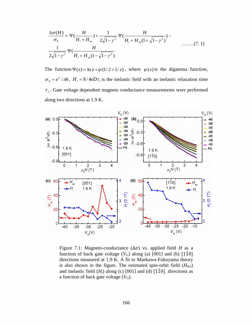
166
)11((
12
1
))11(
(12
1)(
)(
22
220
soi
soisoi
HH
H
HH
H
HH
HH
……. (7. 1)
The function )/12/1(ln)( zzz , where )(x is the digamma function,
he /2
0 , ii eDH 4/ is the inelastic field with an inelastic relaxation time
i . Gate voltage dependent magneto conductance measurements were performed
along two directions at 1.9 K.
Figure 7.1: Magneto-conductance ( ) vs. applied field H as a
function of back gate voltage (VG) along (a) [001] and (b) directions measured at 1.9 K. A fit to Maekawa-Fukuyama theory
is also shown in the figure. The estimated spin-orbit field (HSO)
and inelastic field (Hi) along (c) [001] and (d) directions as
a function of back gate voltage (VG).

167
Figure 7.1a shows the magneto conductance ( ) as a function of the normal
external magnetic field (H) at various gate voltages in [001] direction. It is clear
from the figure that the magneto conductance shows a systematic change with
gate voltages. The experimental magneto conductance curves were fitted with
eqn. (7.1) (Maekawa-Fukuyama theory). Fitting to the equation yield a very good
fit for VG < 0, but the fit is very poor for VG > 0 which could be due to an increase
in Coulomb interactions. Therefore we restrict our discussion to VG < 0. Figure
7.1b show the magneto-conductance measured with various gate voltages along
the direction. The behavior is similar to [001] direction except with a
slightly larger magneto conductance. In this case also the experimental results are
fitted well with eqn. (7.1). The extracted parameters of the fittings, SOI field Hso
and inelastic field Hi, are plotted as a function of VG for [001] and in figure
7.1c and 7.1d respectively.
Here Hso represents a spin relaxation process whereas Hi represents the inelastic
scattering process. The SOI field Hso shows a gradual increase with increase in VG
in both crystal directions; however their magnitudes are very different implying a
significant anisotropy in the spin relaxation. On the other hand the inelastic field
Hi decreases with increase in VG, however their magnitudes are comparable in
both directions.
To further determine the nature of the spin relaxation, the spin relaxation time so
was extracted from soH using soso eDH 4/ where the diffusion coefficient D
is calculated using Einstein relationship, emnD s
*2 / . Here ns is the carrier
density of the sample which is 1.98×10¹³
cm-2
. The effective mass of the electron
in both crystallographic orientations is taken as 0
* 3mm [10], where 0m is the
free electron mass. On the other hand inelastic relaxation time i is calculated
using ii eDH 4/ . Figure 7.2a shows variation in so and i as a function of VG
in [001] and directions respectively.

168
Figure 7.2: Estimated spin relaxation time (so) and inelastic
relaxation time (i) as a function of back gate voltage (VG) along
(a) [001] and (b) directions.
Clearly, in both directions the i shows very small changeas is the cas of the gate
voltage as is the Hi. On the other hand so is tunable with the gate voltage. In both
directions, so is much smaller than the i implying that the spin relaxation is the
dominant mechanism in the transport. In addition, the magnitude of so is
significantly different in [001] and directions further suggesting an
anisotropic nature of the spin relaxation mechanism of the LAO/STO (110)
system. The spin relaxation time in direction is of the order of 0.2 ps with
the spin diffusion length ss Dl is ~10 nm at a VG = -40 V. whereas in [001]
direction at a VG of -40 V, spin relaxation time is about 0.02 ps with sl is 3 nm.
To understand the nature of mechanism of spin relaxation, it is important to
investigate the relation between spin relaxation and elastic relaxation time
where em /* . Figure 7.2b shows the variation in so as a function of inverse
of in [001] and directions respectively. In both directions, clearly there
is an inverse relationship between so and which also exhibits anisotropy. The
inversion relationship of so with confirms the Rashba type SOI at the
LAO/STO (110) interface. Eventhough the applied electric fields are very small
with respect to the atomic potentials, yet the interface carrier confinements and

169
filling of various orbitals can be largely influence by the external electric fields
could have resulted in this large tenability of SOI at this interface.
7.3. Magnetic field direction dependeece of spin-orbit interaction
Figure 7.3: Estimated spin splitting () and coupling constant (α)
as a function of back gate voltage (VG) along (a) [001] and (b)
. (c) Magneto-conductance (MC) at different angles of the
magnetic field H ranging from out of plane (θ = 0ο) to in plane (θ =
90ο). (d) Fitting parameters, Hso and Hi, as a function of the angle
of the magnetic field. Inset is a schematic of the co-ordinate system
showing the direction of the applied field H.
The strength of the SOI, , is calculated which is related to the spin relaxation
time so through the relationship Dmso
2
*
24 8/ . In the presence of broken
inversion symmetry, the dispersion relationship at the Fermi surface exhibits a
splitting in the k-vectors for up and down spins. The spin splitting is given by

170
Fk2 where Fk is the Fermi wave vector which is calculated from carrier
density. Figures 7.3a and 7.3b show the spin splitting energy and the strength
of the SOI as a function of the gate voltage. A spin splitting energy of 10 meV
is estimated for VG=-20 V in [001] case whereas this value is lower for
direction. The spin splitting energy reported here is comparable to those of GaAs
heterostructures. Since the change in carrier concentration is small for the range
of the applied VG, , which is clear from figure 7.3a and 7.3b. To clarify the
nature of the SOI further, we did magneto conductance measurements at VG = -40
V by varying the angle ( ) of the applied magnetic field to the interface, from out
of plane ( 0 ) to in plane ( 90 ) direction which is shown in Figure 7.3c.
The magneto-conductance is fitted with eqn. (7.1) which gives a very good fit to
the experimental results at all angles. As the magnetic field orientation changes
from out of plane to in plane, the negative magneto conductance decreases
indicating that the conduction electron spins are affected by the magnetic field.
The parameters of the fittings soH and iH are given in figure 8.3d as a function of
the orientation of the magnetic field.
7.4. Summary
The gate tunability of SOI coupling at the LAO/STO (110) interfaces certainly
supports the Rashba type SOI at these interfaces. The onother important factor
arised from the present study is the anisotropy in SOI in the (110) plane itself.
One way to produce the anisotropy in SOI is due to the atomic arrangement at the
interface. Along direction, two Ti atoms are connected by an O atom in a
zigzag way, while along [001] direction it is linear. The differences in atomic
arrangements may give rise to different potential gradients along respective
directions. Since the origin of SOI lies in these potential gradients thus an
insitropy in SOI would be expected. Further, generally Rashba effect is expected
to be constant for inplane and out of plane measurements, but we see a change in
strength of SOI from inplane to out of plane suggesting that there can be other
contribution to the spin-orbit interaction other than Rashba type SOI that has been

171
demonstrated before. Thus far the SOI in semiconductor and heavy element
metallic surfaces considers the spin as the source and dominant factor. However,
these oxide materials with transition metals pocess an additional orbital concept
that may have a significant role in the SOI at these oxide interfaces. Few recent
reports suggesting an atomistic SOI and SOI with orbital effects have been
proposed at the LAO/STO interfaces.Thus the atomic and orbital arrangements at
the interfaces may have a significant role in those scenarios. These additional SOI
concepts need to be investigated further for a complete understanding of SOI
theory at the oxide interfaces
172
References
[1] S. Datta, and B. Das, “Electronic analog of the electro‐optic modulator,”
Applied. Physics Letters, 56, 665 (1990).
[2] J. P. Eisenstein, H. L. Störmer, V. Narayanamurti, A. C. Gossard, and W.
Wiegmann, “Effect of Inversion Symmetry on the Band Structure of
Semiconductor Heterostructures,” Physical Review Letters, 53, 2579
(1984).
[3] A. D. Caviglia, M. Gabay, S. Gariglio, N. Reyren, C. Cancellieri, and J. -
M. Triscone, “Tunable Rashba spin-orbit interaction at oxide Interfaces,”
Physical Review Letters, 104, 126803 (2010).
[4] M. Ben Shalom, M. Sachs, D. Rakhmilevitch, A. Palevski, and Y. Dagan,
“Tuning Spin-Orbit Coupling and Superconductivity at the
SrTiO3/LaAlO3 Interface: A Magnetotransport Study,” Physical Review
Letters, 104, 126802 (2010).
[5] K. Michaeli, A. C. Potter, and P. A. Lee, “Superconducting and
Ferromagnetic Phases in SrTiO3/LaAlO3 Oxide Interface Structures:
Possibility of Finite Momentum Pairing,” Physical Review Letters, 108,
117003 (2012).
[6] R. J. Elliott, “Theory of the Effect of Spin-Orbit Coupling on Magnetic
Resonance in Some Semiconductors,” Physical Review, 96, 266-279
(1954).
[7] M. I. D'yakonov and V. I. Perel', Fiz. Tverd. Tela (Leningrad)
13, 3581 (1971) Sov. Phys. Solid State 13, 3023 (1972).
[8] P. D. Dresselhaus, C. M. A. Papavassiliou, and R. G. Wheeler,
“Observation of spin precession in GaAs inversion layers using
antilocalization,” Physical Review Letters, 68, 106-109 (1992).

173
[9] J. Nitta, T. Akazaki, and H. Takayanagi, “Gate Control of Spin-Orbit
Interaction in an Inverted In0.53Ga0.47As/In0.52Al0.48As Heterostructure,”
Physical Review Letters, 78, 1335-1338 (1997).
[10] L. F. Mattheiss, “Energy Bands for KNiF3, SrTiO3, KMoO3, and KTaO3,”
Physical Review B, 6, 4718-4740 (1972).

174

175
Chapter 8
Tuning the interface conductivity at the LaAlO3/SrTiO3
interfaces using proton beam irradiation
Abstract
The structuring and patterning of the 2DEG at the LAO/STO interface for device
measurements and applications have remained a challenging task owing to the
difficulties in physically structuring the oxides. Here, the use of energetic low Z-
ion (proton/helium) beam exposure for engineering the interface conductivity has
been investigated. It is found that this method can be utilized to manipulate the
conductivity at the LAO/STO interface by carrier localization, arising from the
defects created by the ion beam exposure, eventually producing an insulating
state. This process of ion induced defect creation results in structural changes in
SrTiO3 which leads to the creation of rapid polarization fluctuations, as revealed
by the appearance of first-order polar TO2, and TO4 vibrational modes which are
associated with Ti-O bonds in the Raman spectra of the irradiated samples.
Furthermore, magneto transport measurements reveal that the irradiated (un-
irradiated) samples show a negative (positive) magneto-resistance along with
simultaneous emergence of first-order (only second order) Raman modes. These
experiments allow us to conclude that the interface ground state
(metallic/insulating) at the LAO/STO can be controlled by tailoring the defect
chemistry of the SrTiO3 with ion beam exposure. Structures with a spatial
resolution of 5 µm have been fabricated in a single step using a stencil mask. The
ability to create an insulating state locally in the conducting oxides demonstrates a
novel way to structure the conducting state without any extra etching or
intermediate lithography.

176
8.1. Introduction
The structuring of the buried 2DEG at the LAO/STO interface is of equal
importance for device applications and studies of quantum phenomena. Several
methods such as amorphous LAO [1, 2] or AlOx layer deposition [3] as
intermediate steps were employed to structure the conducting regimes. In the
above techniques the insulating state is created by additional deposition steps of
these insulating oxides. Nanoscale writing of conducting structures has been
demonstrated by Atomic force microscopy (AFM) on (3 uc) LAO/STO samples
[4]. However, in all these approaches either the presence of residual hard mask in
the film along with the number of additional sophisticated process steps, or the
stability of the structures in ambient conditions (AFM writing case) is an issue of
concern. Lithography along with reactive ion etching (RIE) has been used
extensively to fabricate controlled structures of various oxide materials. However,
heavy ions present in the commonly used RIE plasma transforms insulating STO
to a conductor [5]. Thus, RIE cannot be applied in patterning of LAO/STO
interfaces. To achieve high quality devices and also to investigate the above-
mentioned exotic phases from these unique interfaces, a reliable and simple
patterning process is essential, which thus far has not been realized. The important
factor in patterning these conducting interfaces is to create a spatially insulating
state. A significant factor is that transition metal oxides are known to show
dramatic changes in electronic properties with the metal-oxygen bonds. The best
examples are metal-insulator transition systems such as VO2 [6] and rear earth
Nickelates [7] where the atomic bonds govern the electrical ground state. Thus the
local structural manipulations involving metal-oxygen bonds in STO may offer a
way to manipulate the electrical transport microscopically. Much to the subject of
effect of atomic bonds, recent reports indicated that the properties of the
LAO/STO system are very sensitive to structural distorsions and epitaxial strain
in STO [8]. Thus modifying the STO structure at local level may offer a new way
to tune the properties of the LAO/STO interfaces. One possible way to manipulate
the lattice structure of a material system locally is by ion beam irradiation where
177
the nuclear and electronic energy loss of the ion beam can alter the lattice
symmetry by possible lattice distortions, and atomic displacements.
In this frame work, a possible manipulation of the properties of 2DEG at
LAO/STO interface can be expected due to ion beam irradiation effects especially
in STO. In the following, the details of ion beam irradiation experiments
performed on LAO/STO interface samples are discussed. The effects of
irradiations on the LAO/STO interface properties were investigated using various
electrical transport measurements and Raman spectroscopy. Scanning Electron
microscope (SEM) was used to image the patterned LAO/STO samples. It is
found that the metallic behaviour of the 2DEG changes significantly with proton
beam exposure, at a fluence of 2×10¹⁷
ions cm-2
strong localization appeared in
the 2DEG, and eventually at a fluence of 6×10¹⁷
ions cm-2
the interface became
insulating. This process of metal to insulator transition occurs through localization
of mobile electrons via ion induced defects, resulting in structural changes in
STO, as revealed by Raman spectroscopy. Raman spectra showed the appearance
of first-order modes of STO which indicate the presence of polar regions in the
irradiated samples. The creation of a spatially-selective insulating ground state by
tuning the process parameters of an energetic ion beam based single step approach
enabled us to both pattern and tune the electronic properties of the 2DEG.
8.2. LaAlO3/SrTiO3 sample preparation for ion beam irradiation
Ion beam irradiation experiments were performed with a 2 MeV proton ion beam
produced using 3.5 MV ion beam facility at the Center for Ion Beam Applications
(CIBA) at the National University of Singapore. The LAO/STO (100) samples
were prepared by pulsed laser deposition by ablating LAO target onto TiO2
terminated STO (100) substrates. Samples were prepared in a range of oxygen
pressure (PO2) of 1-5×10⁻³
Torr at 750 οC. To make a systematic comparison, the
ion irradiation experiments were performed with different proton fluencies on a
single LAO/STO sample that consists of four equal and identical portions (each of
them consist the 2DEG and portions are electrically isolated to each other). The

178
schematic representation is shown in figure 8.1. To achieve samples with four
isolated equal portions, first, precise cross lines were made on to the square STO
(2×2 mm) substrate surface with a diamond cutter that makes it in to four equal
portions. Then LAO film of 8 uc is deposited on the partitioned STO substrate.
Each portion of the deposited LAO/STO sample showed a conducting behaviour
and conductivity is absent between any two portions. The diamond cut lines here
resulted in insulating areas that account for the successful partition of the 2DEG.
Three out of the four sections of the same sample were exposed to proton beam
and the fourth region was kept un-irradiated (as deposited). The ion fluences used
were 1×10¹⁵
, 1×10¹⁶
and 2×10¹⁷
ions cm-2
respectively.
Figure 8.1: A schematic of the LAO/STO sample used for ion
beam irradiations. The values represent the ion fluencies used for
irradiation.
The proton irradiation experiments and measurements were performed on the (8
uc) LAO/STO sample deposited at PO2 of 1×10⁻³
Torr. The typical travelling
depth of 2 MeV proton beam is about 26 µm (micro metres) into the STO

179
substrate. A collimated beam of 2 MeV protons were used to raster-scan under
normal incidence over an area of 2×2 mm2.
8.3. Proton beam irradiation effects on properties of 2DEG
8.3.1 Electric transport and electron localization effects
The electrical transport properties of irradiated portions and as deposited portion
of the (8 uc) LAO/STO sections of sample were measured by PPMS. Electrical
contacts to the buried 2DEG were provided by Al wire bonding to the interfaces.
The temperature dependence of the resistance R (T) for the as-deposited and
irradiated sections is shown in Figure 8.2a. The as-deposited section of the sample
exhibits a typical metallic behaviour similar to the conventional LAO/STO
interfaces at this LAO thickness [9]. Whereas for the irradiated sections, a gradual
change in the resistance at 300 K is observed with increase in ion fluence. As the
proton fluence is increased, clear localization behaviour in transport starts to
emerge at low temperatures with the signature of increased base resistance at 2 K.
The sample section irradiated with 2×10¹⁷
ions cm-2
shows strong localization
with a resistance of 0.1 MΩ at 2 K, and the resistance minimum in the R (T) curve
is found to shift towards higher temperature with an increase in ion fluence. The
above R (T) behaviour gives adequate indication that ion exposure has created a
high resistive state of the 2DEG through localization of the mobile electrons. The
drastic upturns in resistance towards low temperatures is expected for transport
mechanisms such as variable range hopping (VRH) in the strong localization
regime (discussed in chapter 5) and magnetic Kondo scattering [10] at this
interface. The R (T) curve for the case of 2×10¹⁷
ions cm-2
does not show any
saturation even down to 2 K (inset of figure 8.2b) inferring that Kondo scattering
may not be the governing mechanism.

180
Figure 8.2: Electrical transport of as-deposited and 2 MeV proton
beam exposed (8 uc) LAO/STO sample sections. (a) Temperature
dependent resistance of as-deposited and ion beam exposed sample
sections at different proton fluences. (b) Variable range hopping fit
to transport data of ion irradiated with 2×10¹⁷
ions cm-2
fluence,
the inset shows the non-saturating behaviour of corresponding
sample section. (c) Temperature dependence of carrier density (ns)
for as-deposited and 2×10¹⁷
ions cm-2
ion fluence. (d) Reduction in
carrier density δns with ion fluence at 300 K, here δns defined as
the difference in ns of as-deposited and irradiated sample sections
((δns = ns (as-deposited) - ns (irradiated)).
The low temperature resistance behaviour is further analyzed with respect to the
VRH mechanism. In the VRH regime R follows a (1/T) 1/n+1
(n = dimensionality
of the system) dependence. A two-dimensional (n = 2) VRH formula fitting for
the experimental data for a fluence of 2×10¹⁷
ions cm-2
case is given in figure
8.2b and the clear (1/T)1/3
dependence below 20 K indicates the dominant
transport mechanism is VRH in this strong localization regime.

181
The other important quantity that can give further insight to the localization
behaviour is the carrier density (ns). The ns for as-deposited and each irradiated
section of (8 uc) LAO/STO sample were extracted from Hall Effect
measurements. Figure 8.2c shows the temperature dependence of the ns behaviour
for the as-deposited and irradiated with 2×10¹⁷
ions cm-2
. The ns for the as-
deposited section of the sample is about 8×10¹³
cm-2
at 300 K and 3×10¹³
cm-2
at
2 K. In comparison, the irradiated section shows a significant decrease in ns to
about 5×10¹³
cm-2
at 300 K and a further decrease towards low temperatures. The
carrier freeze-out towards low temperature further indicates localization effects
induced by ion beam exposure. Figure 8.2d shows the extracted decrease in
carrier density (δns) with proton fluence at 300 K. Here δns is defined as the
difference in the ns of as-deposited and ns of irradiated sections (δns = ns(as- deposited)
- ns(irradiated)). From Figure 8.2d it is clear that δns increases with the proton fluence
with a value of δns of about 3×10¹³
cm-2
for a fluence of 2×10¹⁷
ions cm-2
. The ns
data clearly indicate that the proton beam exposure with a fluence of 2×10¹⁷
ions
cm-2
can reduce as many as 3×10¹³
cm-2
mobile carriers of the 2DEG at the
interface which is most possibly accomplished by localization of carriers within
the lattice of STO. From the above conclusion one may expect that the interface
samples having initial ns ≤ 2-3×10¹³
cm-2
may turn insulating at these ion fluences
due to complete localization of carriers. Further to validate this possibility, a
conducting LAO/STO sample having an initial carrier density of 1.9×10¹³
cm-2
(achieved by controlling the oxygen pressure during the growth) has turned to
became insulating with the exposure of proton beam at a fluence of 2×10¹⁷
ions
cm-2
.
From the above conclusion one may expect that the interface samples having
initial carrier density in the order of 3-4×10¹³
cm-2
may turn in to insulating state
at these ion doses due to the complete localization of carriers. To verify the above
possibility, new LAO/STO sample was grown at slightly higher PO2 of 5 ×10⁻³
Torr with LAO thickness of 5 uc. The sample ns is found to be 2×10¹³
cm-2
at 300
K which is lower than the previously discussed sample (the reduced ns achieved
by growing the sample at relatively high PO2). A portion of the new sample was

182
irradiated with the proton ion dose of 2×10¹⁷
ions cm-2
. Strikingly as anticipated
this irradiated portion become insulator (exceeding measurement limit of 20 MΩ).
The above experiment on the sample with low ns (2×10¹³
cm-2
) confirms that ion
irradiation can completely localize the ns of the order of 3-4×10¹³
cm-2
with ion
dose of 2×10¹⁷
ions cm-2
.
8.3.2 Magneto resistance analysis
Figure 8.3: Magnetoresistance (MR) of the (8 uc) LaAlO3/SrTiO3
sample sections with different proton fluences: (a) Out of plane
MR at 2 K for different ion fluences. (b) Out of plane MR at 2, 5,
10 and 20 K for the sample section irradiated with 2×10¹⁷
ions cm-
2. (c) In-plane and out of plane MR measured for the sample
section in (b) at 2 K. (d) Angle dependent anisotropic magneto
resistance measurement for the corresponding sample portion.
183
To evaluate the localized transport behaviour at low temperature in the above ion
exposed samples, a detailed magnetoresistance (MR) study was carried out. MR is
a useful tool to investigate the transport mechanisms such as localization and
magnetic scattering. MR measurements were performed in various modes such as
in-plane, out of plane and anisotropic MR (AMR). Figure 8.3a shows the out of
plane MR (magnetic field H perpendicular to the interface) measured for different
ion irradiation fluences and as-deposited sections at 2 K with H upto 9 T. Both as-
deposited and low fluence (1×10¹⁵
ions cm-2
) sections display a positive MR
behaviour. Positive MR is a characteristic of orbital scattering in the presence of a
magnetic field due to the change in electron transit paths. On the other hand the
section exposed with 2×10¹⁷
ions cm-2
fluence shows a negative MR behaviour.
Comparison of the MR with respect to ion fluence infers that the MR slowly
changes sign from positive to negative with increasing ion fluence, suggesting
that it must be correlated with the localization effects discussed earlier in figure
8.2. The large negative and non-saturating MR observed in the irradiated case is a
further indication of strong localization behaviour. Electron transport in the
strongly localized regime can exhibit a negative MR as a consequence of
magnetic field disrupting the self-interference of the electrons and is consistent
with the VRH study (discussed in chapter 5). The temperature dependence of the
out of plane MR measured for a fluence of 2×10¹⁷
ions cm-2
is shown in Figure
8.3b. The magnitude of MR gradually decreases with increase in temperature
which can be understood as the effect of enhanced thermal fluctuations on the
scattering process. Figure 8.3c shows the comparison of in-plane (H applied
parallel to the interface) and out of plane MR for the 2×10¹⁷
ions cm-2
case where
both display a negative MR, however with a difference in MR magnitude. Orbital
scattering is excluded in this in-plane geometry due to the absence of Lorentz
forces on carriers. The in-plane anisotropic MR (AMR) measurement performed
for the 2×10¹⁷
ions cm-2
case and with rotated the H with respect to current (I)
direction within the plane of the interface is shown in figure 8.3d. The AMR
shows an oscillatory behaviour which is similar to that discussed in chapter 4.

184
The detailed electron transport and MR analysis discussed above clearly indicates
the dependence of ion fluence for carrier localization and point towards the
possibility of creating insulating regions in 2DEG. At the LAO/STO interface it is
known that the 2DEG is accumulated at the Ti orbitals of STO [11]. Since the ion
irradiation produces dramatic changes in the transport of the 2DEG that resides in
STO, it is necessary to understand the effects of ion irradiation on STO. Recent
reports on STO based interfaces reveal that an atomic distortion of the STO lattice
at the interface can manipulate the transport properties of 2DEG significantly [8,
12]. Direct implications of irradiation are that it may create distortions in the
crystalline lattice of STO, and/or it may create various types of vacancies and
local disorder to an extent in the STO during the various energy-loss processes. A
significant observation made with ion irradiation is the optical contrast of the
irradiated portions of the sample. The irradiated portions lost the transparency
when compare to the as deposited LAO/STO sample portion. In general, ion
irradiation can be expected to modify the atomic structure of the materials through
electronic and nuclear energy-loss with the atoms of the materials. These atomic
structural changes may in turn modify the properties such as optical transparency
and electron transport as shown above. In order to investigate the ion irradiation
effects on structural and electronic properties of the LAO/STO samples, Raman
spectroscopy experiments were carried out.
8.4. Raman spectroscopy of irradiated LaAlO3/SrTiO3 interface
To understand the possible microscopic structural changes in LAO/STO samples
with ion irradiations, Raman spectroscopy experiments were performed on
pristine and irradiated portions of the LAO (8 uc) /STO sample. Visible Raman
spectroscopy was carried out at room temperature using Renishaw Invia system.
The excitation wavelength used was 532 nm and the laser power at the sample
was below 1.0 mWcm-2
to avoid laser induced damage. A 50X objective lens was
used with a laser spot size of ~1 µm and the scattered light from the sample was
collected in the back scattering geometry. Raman imaging was carried out using
WITec CRM200 Raman system using 532 nm excitation wavelength with a
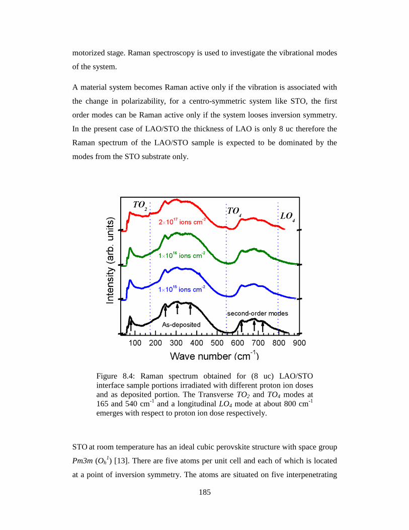
185
motorized stage. Raman spectroscopy is used to investigate the vibrational modes
of the system.
A material system becomes Raman active only if the vibration is associated with
the change in polarizability, for a centro-symmetric system like STO, the first
order modes can be Raman active only if the system looses inversion symmetry.
In the present case of LAO/STO the thickness of LAO is only 8 uc therefore the
Raman spectrum of the LAO/STO sample is expected to be dominated by the
modes from the STO substrate only.
Figure 8.4: Raman spectrum obtained for (8 uc) LAO/STO
interface sample portions irradiated with different proton ion doses
and as deposited portion. The Transverse TO2 and TO4 modes at
165 and 540 cm-1
and a longitudinal LO4 mode at about 800 cm-1
emerges with respect to proton ion dose respectively.
STO at room temperature has an ideal cubic perovskite structure with space group
Pm3m (Oh1) [13]. There are five atoms per unit cell and each of which is located
at a point of inversion symmetry. The atoms are situated on five interpenetrating

186
simple cubic lattices and at the Brillouin zone center, all the optical phonons in
the cubic phase are of odd parity, which accounts for the absence of first-order
Raman scattering in STO single crystals [14-16]. Even though the first-order
modes are Raman inactive, STO shows a Raman spectrum with broad peaks that
are arising from higher-order modes which involves the creation or destruction of
two or more first-order modes. Raman spectrum was collected for irradiated and
as deposited portions of the (8 uc) LAO/STO sample and is shown in the figure
8.4. As expected the spectrum is dominated by STO modes. In the spectrum, the
broad second-order peaks are clearly visible at 75, 200-500 and 600-800 cm−1
which arise from the second order-order modes. Significantly, additional peaks
start to emerge at 175, 540 and 795 cm-1
with increase in irradiation ion fluences
(clearly visible for the sample portion irradiated with proton ion fluence of 2×10¹⁷
ions cm-2
). These peaks are identified as symmetry-forbidden first order modes
arising from transverse TO2, TO4 and longitudinal LO4 phonons, respectively [17-
19]. A significant note here is that the appearance of these Raman modes co-
insides with the evolution of localization behaviour in electric transport
measurements with respect to the ion irradiation fluence where the highest fluence
show maximum effects with change in both Raman spectrum and transport. The
appearance of first-order modes in irradiated portions of the sample clearly
indicates a lowering of crystal symmetry for the STO and thus the loss of the
inversion centre [17-19]. First-order Raman scattering has been observed in thin
films, nano-structures of STO, and also in single crystals with lifted centre-of-
symmetry by the application of an external electric field [18-20]. The line shape
of the TO2 peak is asymmetric- i.e. the scattering intensity increases at the high-
energy side and is depressed at the low-energy side of the peak- and this displays
a Fano profile [17-19]. Fano effect occurs whenever discrete excitations and a
broad continuum interfere coherently.
This continuum of excitations in the
irradiated sample is polar because it interacts with the polar TO2 phonon. Such
asymmetric line shapes have been observed for polar TO2 modes in STO thin
films and have been ascribed to the interaction of the phonon with a continuum
arising from rapid polarization fluctuations [17, 18]. Although TO4 is also a polar

187
phonon, its energy is much higher, the density of states for continuum vanishes at
this frequency and thus Fano asymmetry has not been observed in the case TO4
mode [17]. The origin of the TO2 and TO4 modes is associated with Ti-O bonding
in the STO [18-20]. The appearance of TO2,4 modes indicate the presence of polar
regions in the case irradiated at a ion fluence of 2×10¹⁷
ions cm-2
.
8.5. Raman spectroscopy of irradiated SrTiO3
In order to further confirm the above spectrum analysis on STO proton irradiation
experiment was carried on bare STO substrate (ion fluence is 2×10¹⁷
ions cm-2
).
The corresponding Raman spectrum for bare STO substrate and irradiated portion
of STO is shown in figure 8.5. Here also a clear emergence of additional modes
(marked in figure with line) are seen for the irradiated sample while they are
absent for bare STO.
Figure 8.5: Raman spectrum obtained for bare STO sample portion
with and without irradiation.

188
Oxygen ions being the lightest in the STO lattice have maximum displacements
compared to Ti, Sr under the exposure of energetic ions. If this is the case, one
would expect a reduction in resistance for the irradiated STO. The conductivity of
the same sample is measured before and after irradiation, and it does not show
any change in the insulating nature of the STO within the sensitivity of our
measurements. This confirms that the current irradiation experiments are not
creating any significant amount of oxygen vacancies to increase the mobile
charges in STO. Eventhough the produced oxygen vacancies may have a chance
of getting compensated by the counter produced cationic vacancies of Sr and Ti.
An estimate of the defects created by the proton beam can be determined from
Monte Carlo simulations (SRIM 2008) using a full damage cascade. Oxygen ions
being the lightest in the STO lattice have maximum displacements compared to Ti
and Sr under irradiation by energetic ions. If oxygen vacancies were the dominant
defects in the MeV proton irradiated STO, one would expect a reduction in
resistance for the irradiated STO as observed by Kan et al. [5]. The displacement
per atom (dpa) for Sr and Ti is found to be half that of oxygen. The oxidation
states of O, Ti and Sr are -2, +4 and +2 respectively. Thus the cationic and anionic
vacancies will have different charges. The conductivity of the same LAO/STO
sample measured before and after irradiation showed an increase in 2DEG
resistance with fluence. In a separate experiment, a STO substrate irradiated with
a fluence of 2×10¹⁷
ions cm-2
did not show any change in the insulating nature of
the STO within the sensitivity of our measurements. This confirms that the
current irradiation experiments does not simply create oxygen vacancies alone,
but also generate compensating cationic vacancies, and at higher fluences other
defect complexes which can trap charges efficiently. This is a benefit as the low Z
ion beam will not produce a parallel conducting path in the STO as in the cases
with low energy heavy ion irradiations [5].
One significant observation from both transport and Raman measurements is that
the sample irradiated with low fluence (1×10¹⁵
ions cm2) does not show much
signature of localization and at the same time no significant changes in Raman
spectrum, where as for the high ion dose of 1×10¹⁷
ions cm-2
irradiation case, both

189
localization behaviours with the formation of polar modes in STO can be noted. It
suggests that the emergence of these polar modes in STO must have a correlation
with electronic structure of STO. The newly learned mechanism to localize
carriers and ability to create insulating state locally as shown above encouraged us
to investigate the structuring capability of the LAO/STO interface.
8.6. Structuring of LaAlO3/SrTiO3 interface
For this, a sample of (8 uc) LAO/STO is grown under identical conditions as the
previous sample. Two lines each of which having dimensions of 500 µm width
and 2 mm in length were patterned in one of the region.
Figure 8.6: Raman spectrum obtained for LAO/STO sample
portions irradiated with different proton ion doses. Schematic
represents the 500 m patterns line made with different proton ion
dose.

190
These three regions were formed by employing ion irradiation with different
doses as shown in figure 8.6. To confirm the the lattice effects of STO the Raman
spectrum is obtained for these three patterned lines. As shown in figure 8.6 the
Raman spectrum displays similar behaviour as in the previous case. Note here is
that the increased ion dose to 6×10¹⁷
ions cm-2
is strongly reflected with
observation of stronger intensity profile for the polar mode peaks in the spectrum
also. Further, a Raman spectroscopy image produced using the integrated
intensity of TO4 mode at 540 cm-1
of the irradiated sample is shown in figure 8.7.
Figure 8.7: Raman spectrum mapped for a TO4 mode at 540 cm-1
for patterned lines (500 µm) of LAO/STO sample portions
irradiated with different proton ion doses showing a clear intensity
difference with ion irradiation dose. The resistance behaviour with
temperature measured for the corresponding patterned lines
displaying the metal to insulator transition with increase in proton
ion irradiation dose.
The as deposited and the irradiated regions at ion dose of 2×10¹⁷
ions cm-2
and
6×10¹⁷
ions cm-2
are clearly distinguishable in the intensity profile. Here as
deposited portion (with electrically conducting state) shows no signal from TO4
mode. Whereas patterned line with 2×10¹⁷
ions cm-2
(strong localization) show a

191
significant intensity of TO4 mode indicating the structural changes in STO at this
dose. The highest intensity of the TO4 mode is observed for the 6×10¹⁷
ions cm-2
doses, which is found to be electrically insulating. Raman imaging thus serves as
an indirect mapping of the interface conductivity of the ion-beam patterned
LAO/STO system.
To show the patterning capability for device applications, the LAO/STO sample
was covered by a stencil mask which is thick enough to stop the ion beam and ion
irradiation was performed with the optimized parameters (fluence of 6×10¹⁷
ions
cm-2
for 2 MeV protons) to create spatially selected regions exhibiting an
insulating state at the interface 2DEG. Figure 8.8a shows a scanning electron
microscopy (SEM) image of the patterned LAO/STO sample using a metal stencil
mask (made from 0.5 mm thick brass) with a Hall bar geometry (channel width
~150 µm) after 2 MeV proton irradiation. As shown in figure 8.8a, the Hall bar
structure has been transferred to the sample with the expected dimensions.
Significantly, the SEM image shows the contrast between the irradiated and as-
deposited sections. The contrast for the secondary electrons at the conducting (as-
deposited) and insulating (irradiated) regimes is due to the difference in the
number of secondary electrons reaching the Everhart-Thornley detector used in
the SEM. We have also explored low energy helium ion irradiations (500 keV) to
create localization and insulating state in conducting LAO/STO interfaces as
discussed earlier. An insulating state is found to be created at a fluence of 1×10¹⁶
ions cm-2
and strong localization at 1×10¹⁵
ions cm-2
in the case of helium ions. A
pattern was formed with a gold mask for helium ion irradiation and is shown in
figure 8.8b. Here, the 5 µm conducting regions (the bright contrast) which are
clearly visible in SEM micrographs demonstrate the capability to pattern the
interface down to lower dimensions. This demonstrates the ability to pattern the
LAO/STO interfaces using low Z-ions without any intermediate deposition or
etching techniques that were previously employed.

192
Fugure 8.8: (a) Scanning electron microscopy (SEM) image of the
patterned LAO/STO sample: (a) using a 2 MeV proton fluence of
6×10¹⁷
ions cm-2
with a mask of Hall bar geometry (in this case
proton beam (6×10¹⁷
ions cm-2
) was irradiated on to the sample
using a tensile metal mask; the irradiated portion locally become
insulating allows patterning the structure). (b) 500 keV helium ions
at a fluence of 1×10¹⁶
ions cm-2
with a gold mask of size 5 µm.

193
8.7. Summary
In this chapter, it is demonstrated that conductivity of the 2DEG at the LAO/STO
can be tuned by the proton beam irradiation. The creation of insulating ground
state in 2DEG locally at higher ion fluence as shown here is of important for the
device applications. The real advantage of this process is that one can pattern the
structures of LAO/STO interfaces locally by employing focussed ion beam
writing. It is advantageous to use protons considering the difficulties to structure
oxide heterostructures especially involving STO with large Z ion beam
irradiations such as Ar+ beam where it has been shown to induce the conductivity
in STO by producing large amount of oxygen vacancies which is undesired to
STO based two-dimensional electron gas systems. The novel way to avoid this
possibility to use low Z-element ion irradiations (proton, helium) as demonstrated
here may open up new way to create structuring of fascinating interface systems
whose properties sensitive to the crystal structure. With the development of
helium ion microscope with focused ion beams having spatial resolutions of sub
0.5 nm, direct patterning of fine conducting lines may be possible on the nm
scale. The correlation between lattice structure and electronic properties is found
to be key to manipulate the properties in these oxide interfaces and may
applicable to other oxide systems whose properties are sensitive to the meteal-
oxygen bonds.

194
References
[1] C. W. Schneider, S. Thiel, G. Hammerl, C. Richter, and J. Mannhart,
“Microlithography of electron gases formed at interfaces in oxide
heterostructures,” Applied Physics Letters, 89, 122101 (2006).
[2] D. Stornaiuolo, S. Gariglio, N. J. G. Couto, A. Fête, A. D. Caviglia, G.
Seyfarth, D. Jaccard, A. F. Morpurgo, and J.-M. Triscone, “In-planeelectronic
confinement in superconducting LaAlO3/SrTiO3 nanostructures,” Applied
Physics Letters, 101, 222601 (2012).
[3] N. Banerjee, M. Huijben, G. Koster, G. Rijnders, “Direct patterning of
functional interfaces in oxide heterostructures,” Applied Physics Letters, 100,
041601 (2012).
[4] C. Cen, S. Thiel, G. Hammerl, C. W. Schneider, K. E. Andersen, C. S.
Hellberg, J. Mannhart, and J. Levy, “Nanoscale control of an interfacial
metal–insulator transition at room temperature,” Nature Materials, 7, 298-302
(2008).
[5] D. Kan, T. Terashima, R. Kanda, A. Masuno, K. Tanaka, S. Chu, H. Kan, A.
Ishizumi, Y. Kanemitsu, Y. Shimakawa and M. Takano, Nature Materials, 4,
816-819 (2005).
[6] N. F. Mott and L. Friedman, “Metal-insulator transitions in VO2, Ti2O3 and
Ti2-x V xO3,” Philosophical Magazine, 30, 389 (1974).
[7] M. L. Medarde, “Structural, magnetic and electronic properties of RNiO3
perovskites (R = rare earth),” Journal of Physics: Condensed Matter, 9, 1679
(1997).
[8] F. Schoofs, M. A. Carpenter, M. E. Vickers, M. Egilmez, T. Fix, J. E.
Kleibeuker, J. L. MacManus-Driscoll, M. G. Blamire, Carrier density
modulation by structural distortions at modified LaAlO3/SrTiO3 interfaces. J.
Phys. Condens. Matter, 25, 175005 (2013).

195
[9] C. Bell, S. Harashima, Y. Hikita, H. Y. Hwang, “Thickness dependence of the
mobility at the LaAlO3/SrTiO3 interface”. Apllied Physics Letters, 94, 222111
(2009).
[10] A. Brinkman, M. Huijben, M. Van Zalk, J. Huijben, U. Zeitler, J. C. Maan, W.
G. Van Der Wiel, G. Rijnders, D. H. A. Blank, and H. Hilgenkamp,
“Magnetic effects at the interface between non magnetic oxides,” Nature
Materials, 6, 493-496 (2007).
[11] M. Salluzzo, J. C. Cezar, N. B. Brookes, V. Bisogni, G. M. De Luca, C.
Richter, S. Thiel, J. Mannhart, M. Huijben, A. Brinkman et al. “Orbital
Reconstruction and the Two-Dimensional Electron Gas at the LaAlO3/SrTiO3
Interface”. Phys. Rev. Lett. 102, 166804 (2009).
[12] H. W. Jang, D. A. Felker, C. W. Bark, Y. Wang, M. K. Niranjan, C. T.
Nelson, Y. Zhang, D. Su, C. M. Folkman, S. H. Baek, et al. “Metallic and
insulating oxide interfaces controlled by electronic correlations”. Science 331,
886 (2011).
[13] R. A. Cowley, “Lattice dynamics and phase transitions of strontium titanate,”
Physical Review, 134, A981-A997 (1964).
[14] W. G. Nilsen, and J. G. Skinner, “Raman spectrum of strontium titanate,” The
Journal of Chemical Physics, 48, 2240-2248 (1968).
[15] A. Tenne. Dmitri, “Raman spectroscopy of ferroelectric thin films and
superlattices,” Journal of American Ceramics Society, 91, 1820–1834 (2008).
[16] Yu. I. Yuzyuk, “Raman scattering spectra of ceramics, films, and superlattices
of ferroelectric perovskites: A Review,” Physical Solid State. 1026-1059
(2012).
[17] A. A. Sirenko, I. A. Akimov, J. R. Fox, A. M. Clark, H. Li, W. Si, and X. X.
Xi, “Observation of the first-order Raman Scattering in SrTiO3 thin films,”
Physical Review Letters, 82, 4500 (1999).
[18] B. Sarbajit, Dae. -In. Kim, R. Richard Robinson, P. H. Irving, Y. Mao, S.
Wong, “Observation of fano asymmetry in Raman spectra of SrTiO3 and

196
CaxSr1−xTiO3 perovskite nanocubes,” Applied Physics Letters, 89, 223130
(2006).
[19] X. W. Wu, D. J. Wu, and X. J. Liu, “Negative pressure effects in SrTiO3
nanoparticles investigated by Raman spectroscopy,” Soild State
Communications, 145, 255-258 (2008).
[20] P. A. Fleury, and J. M. Worlock, “Electric-field-induced Raman scattering in
SrTiO3 and KTaO3,” Physical Review, 174, 613-623 (1968).

197
Chapter 9
Conclusion and scope of future work
9.1 Conclusion
9.1.1 Magnetic interactions
In this thesis work the nature of magnetic interactions at the LAO/STO system
were investigated through the AMR and PHE measurements. A fourfold
oscillation behavior in the AMR is observed for the confined 2DEG, and a
twofold oscillation observed for the 3D case. The origin of the fourfold oscillation
primarily arising from magnetic interactions of itinerant electrons with localized
magnetic moments coupled to the crystal symmetry via spin-orbit interaction. The
observation of this behavior only for the confined 2DEG case infers that the
magnetic interactions are predominant at the interface. The observed PHE further
signifies that the predominant in-plane component of the magnetization in the
system supports the previous observations. The role of spin-orbit interaction is
verified by the tunability of magnetic interactions at the interface. The AMR and
PHE measurements are very useful as a probe for the magnetic interactions in low
dimensional systems.
9.1.2 Strain and correlation effects at polar/non-polar oxide interfaces
It is shown that the new combinations of various polar/non-polar oxides interfaces
namely, NdAlO3/ SrTiO3, PrAlO3/SrTiO3 and NdGaO3/ SrTiO3 can also support
the 2DEG at the interface. This study offered new interfaces to further investigate
and tune the properties at these polar/non-polar oxide interfaces. A detailed
transport analysis revealed that the properties of the 2DEG can be influenced by
the polar over layers. This study inferred that the combined effects of interface
strain and electron correlations offered by polar layers can play a crucial role at
these oxide interfaces. The lattice-mismatch of various polar layers with STO can
induce considerable octahedral distortions in STO. Even though naive thinking is
198
that the bulk substrates expected to induce the strain in over layers, however this
study shows that at the interface the substrate layers is also influenced by the over
layers to an extent that can manipulate the interface physics and properties as the
case here. The observations such as rare earth (RE) cation dependence of carrier
density, lattice mismatch effects on mobility offered by polar layers may provide
an opportunity to tune the properties at selected polar/non-polar oxide interfaces.
Further, the observed thickness dependence of metal-insulator transition for the
NdAlO3/SrTiO3 interfaces suggest that polar discontinuity may possibly be the
prime origin of conductivity at these polar/non-polar interfaces as well. The
thickness dependence of localization effects of 2DEG are observed at the
NdAlO3/SrTiO3 interfaces. In the strong localized regime the transport is
governed by variable range hopping. These results emphasize the dominant role
of over layer thickness in controlling the transport properties of 2DEG at these
interfaces through the interface strain effects. Moreover, the study presented in
this report can help in distinguishing localization from other mechanism which is
very important in understanding the physics of electron transports in two
dimensional oxide systems.
9.1.3 Anisotropic conductivity at (110) interfaces
The importance of the unexpected conductivity demonstrated at (110) interfaces is
better brought into context with what has been learnt so far with the (100)
interfaces. The 2DEG at the LaAlO3/SrTiO3 (100) interfaces has been studied
under a variety of deposition conditions, layer thicknesses and externally applied
fields. In most of these experiments the 2DEG was presumed to be the result of a
direct manipulation of electrostatic potential at the interface in order to promote
electrons to the conduction band of STO, which requires energy of the order of
3.2 eV. Our experiments and DFT calculations using (110) substrates show that
the polarization catastrophe model may still be valid for crystalline LAO/STO
interfaces provided the interface is viewed appropriately in (110) case (buckled
interface). The real attraction of these LAO/STO (110) interfaces is that they offer

199
a new physical parameter which is crystalline anisotropy. The demonstrated
anisotropy in mobility is very significant for the anisotropic devices at nano-scale.
9.1.4 Tuning the interface conductivity with ion beam irradiation
In this study it is shown that properties of the 2DEG at the LAO/STO can be
tuned by the proton beam irradiation technique. The creation of insulating ground
state in 2DEG locally as shown here is of important for the device applications.
The real advantage of this technique is that one can pattern the structures of
LAO/STO interfaces locally by employing focussed ion beam writing. Further,
considering the difficulties in patterning of oxide heterostructures especially
involving STO with heavy ion beam irradiations such as Ar+ beam where it has
been shown to induce the conductivity in STO by producing large amount of
oxygen vacancies which is undesired to STO based 2-dimensional electron gas
system. The novel way to avoid this is to use low Z-element ion irradiations as
demonstrated may open up new way to create structuring of fascinating interface
systems whose properties sensitive to the crystal structure. The correlation
between the lattice structure and electronic properties is found to be key to
manipulate the properties in these oxide interfaces and may applicable to other
oxide systems also whose properties are sensitive to the meteal-oxygen bonds.
The patterning ability of the 2DEG with direct ion beam exposure without using
any intermediate lithography processing steps as shown here is of technological
importance.
9.1.5 Nature of spin-orbit interaction
The observation of quasi-two dimensional electrical conductivity at the
LaAlO3/SrTiO3 (110) interface has generated much interest due to its possible
potential in crystallography dictated low dimensional devices. Our angle
dependant magneto-conductance results clearly show that there two contributions
to the SOI, one originating from the normal component of the conduction electron
spin and other from the Rashba effect arising from in-plane spin components.
Here we suggest that the interface exhibits a strong anisotropic type z-component
200
SOI with respect to the crystallography. The anisotropy is understood to arise
from the difference in the potentials associated with Ti t2g orbitals along [001] and
directions. Both z-component SOI and Rashba SOI is gate tunable which is
technologically very promising. Above all we have shown here a possible route to
tune the interface SOI by varying the potential gradient arising from atomic
arrangements at these anisotropic interfaces.
9.2 Scope of future work
9.2.1 Role of crystallography on orbital reconstructions and magnetism
The demonstrated strong magnetic interactions at the interface with respect to
carrier confinement and electric fields are very important for the implementaiton
of spintronic based concepts to the LAO/STO interfaces. The present study shows
that these properties are very sensitive to the dimensionality and growth condition
of the interfaces is very crucial to realize these magnetic interactions. The present
study can be further explored with respect to the crystallography. Based on recent
observation of 2DEG at other oriented interfaces (including our study of 2DEG at
(110)-oriented interfaces), theroritical reports further suggested that magnetic
ordering could depend on interface orientation where the orbital hybridizations
play a crucial role. One best way to cross check these predictions is by performing
these anisotropic measurements on various oriented interfaces such as along (110)
and (111). The comparision study may give the information about such orbital
hybridization picture at these interfaces.
9.2.2 Exploring the 2DEG properties at anisotropic surfaces
In this thesis work it is further demonstrated that the 2DEG show highly
anisotropic nature with respect to the crystallographic directions. The presence of
linear and zig-zag Ti-O-Ti chains along two directions opens up new possibilities
for nanoscale quantum phenomena. For example, the anisotropy can be further
explored by nano-structuring the 2DEG along the anisotropic crystallographic
directions with techniques such as conducting atomic force microscopy (AFM)
201
charge writing which is already shown to create new properties. Further,
investigation of the anisotropy on other phenomena (magnetism,
superconductivity) will be of interest which may lead to new physics and device
applications. Further, given the fact that the spin-orbit interactions can arise from
the symmetry breaking near the interfaces and these in-plane anisotropic
interfaces readily offer symmetry breaking within the plane of interface which
would further attract a lot of interest to explore the electric field effects on these
anisotropic surfaces. In this thesis work we have shown the signature of such
anisotropic nature of spin-orbit interactions. These experimental observations can
be further explored through theoretical understanding of the spin-orbit interaction
concept. In complex oxides, spin as well as orbital degrees of freedom are very
sensitive to the external stimuli; therefore one needs further investigation of spin-
orbit interactions. Further analysis of spin-orbit interactions with respect to the
crystallography is of importance.
9.2.3 Towards single step nano-structuring of interfaces with ion beams
Using an ion beam (proton/helium), a single-step structuring capability of
LAO/STO interfaces down to 5 µm using a hard mask.exposure technique has
been demonstrated. However focussing of these ion beams, utility of hard masks
with lateral dimentions limits the structuring. This can be overcome by using the
newly developed focused ion beam microscopes for example helium ion
microscope which has a capability of focussing the energetic ions beams down to
nanometer level. As a future direction these interfaces can be tested for the
patterning with the helium ion microscope. Further, tailoring interface
conductivity locally by tuning the interface defect chemistry is a novelty of this
work. This ion beam exposure technique can be explored on other complex oxides
that are sensitive to the metal-oxygen bonds. For example rare earth nickels
oxides and vanadium oxide systems, whose properties are very sensitive to the
chemical bonds. The possible manipulation of local structure in these materials
may allow tuning the material properties and may allow patterning them also.