electron transit-time and exit velocity in linear beam ... · electron transit-time and exit...
TRANSCRIPT

Electron Transit-Time and Exit Velocity in Linear Beam Travelling Wave
Amplifier for a Dielectric Rod Supported Tape-helix Slow Wave
Structure
Richards Joe Stanislaus1, Gnanamoorthi Naveen Babu2
Department of Electrical Engineering,School of Engineering,
Shiv Nadar University, [email protected], [email protected]
Richards Joe S/IEEE INAE/2016-12-13
(Presented at the IEEE-INAE Symposium on Electromagnetic Education and Research, SSN College of Engineering, Tamil Nadu, India, December 12-13, 2016)
1
Forum for Electromagnetic Research Methods and Application Technologies (FERMAT)

Copyright
©The use of this work is restricted solely foracademic purposes. The author of this workowns the copyright and no reproduction inany form is permitted without writtenpermission by the author.
Richards Joe S/IEEE INAE/2016-12-13 2

Abstract
The large signal behavior of linear beam travelling waveamplifier is presented in this paper. The electron transit timeand the electron exit velocity in a dielectric supported helixtraveling wave tube amplifiers (TWTA) are derived by solvingthe non-homogeneous boundary value problem. From theMaxwell’s field equations, electron ballistic equation and fromthe boundary conditions of the tape helix TWT, a Green’sfunction sequence is obtained for the axial electric field as afunction of electron arrival time in the interaction region. Bysuccessive approximation technique, the electron transit timeand therefore the exit velocity equations were derived andnumerically computed.Keywords: Electron ballistic equation; anisotropicallyconducting, tape-helix, electron beam; boundary conditions
Richards Joe S/IEEE INAE/2016-12-13 3

BiographyRichards Joe Stanislaus obtained his BE(ECE) and ME(Communication Sysems)from Government College of Engineering Tirunelveli, India (2009) and College ofEngineering Guindy, Anna University, India(2011) respectively. He worked in TataConsultancy Services, Chennai for 2 years (2011-2013) as Systems Engineer. Atpresent, he is in his 4th year of Doctoral Studies (ECE) at Dept of ElectricalEngineering, School of Engineering, Shiv Nadar University, U.P., India (2013-Present).During the course of his doctoral study, he has assisted in the courses Introduction toElectrical Engineering, Digital Signal Processing, VLSI Design, Microprocessors andMicrocontrollers and Electrical Machines.He has two journal papers(IET Microwave, Antenna and Propagation and IJMOTL)and has presented his research papers in 3 IEEE international conferences out of whichhe received best presented paper award in ICCCET 2011. He also possess 6 nationalconference papers. He has received hands on training and is proficient in CST ParticleStudio, CST Microwave Studio, HFSS, Advanced Design Systems and MATLABprogramming. He also has experience in Cadence Virtuoso, Java J2EE and Cprogramming. His research area of interest includes Microwave Tubes, Antennas andElectromagnetics – Theoretical modelling, Numerical computation and 3D analysis.
Richards Joe S/IEEE INAE/2016-12-13 4

Gnanamoorthi Naveen Babu obtained his BE(EEE) and ME(Applied Electronics) from Amrita Instituteof Technology and Science, Coimbatore, India(2002) and P.S.N.A. College of Engineering and Technology,Dindugal, India(2004) respectively. He completed his doctoral studies and was awardedPh.D(Electromagnetics) from Jaypee Institute of Information and Technology, Noida, India(2013). He wasPost Doctoral Fellow at University of Alberta, Edmonton, Canada for one year. He was lecturer at PSNACollege of Engineering and Technology(2004-2005) and Jaypee Institute of Information andTechnology(2005-2008). He was Senior Lecturer in Jaypee Institute of Information and Technology(2008-2011). He joined Shiv Nadar University at 2011 and was Assistant Professor for 3.5 years in which he wasCo-ordinator of ECE and EE Departments for 1 year and 4 months. After his PostDoctoral studies, he onceagain joined Shiv Nadar University in 2015 and has been there as Assistant professor ever since.He has 9 publications at renowned journals (IEEE Transactions on Antenna and Propagation, IETMicrowave Antenna and Propagation, IJACS Elsevier, PIER B, etc). He has authored and co-authored 17books and has presented in 9 international conferences and 13 national conferences and has attended 20national workshops. He has been reviewer for IEEE Transactions on Microwave Theory and Techniques,PIER and was invited member and guest at International Editorial Scientific Board, Advances in ElectronicEngineering, International Journal of computing and Digital Systems, UK, and seven other events.He has guided many BE students in over 25 major and minor projects and is presently guiding a Ph.Dresearch scholar at Shiv Nadar University, Greater Noida, India. He is an active member in variouscommittees including admissions, managing events, departmental responsibilities, administrative skills, etc.He currently continues to work on slow wave structures, fast wave analysis of slow wave structures,fundamental electromagnetic theory, and microwave circuits and antennas. His research area is MicrowaveEngineering with focus towards travelling wave tubes. He also works on metamaterial dielectric lenses anddesign of antennas. He has interests in renewable energy and energy auditing procedures. He brings withhim more than 11 years of teaching experience.
Richards Joe S/IEEE INAE/2016-12-13 5
Biography
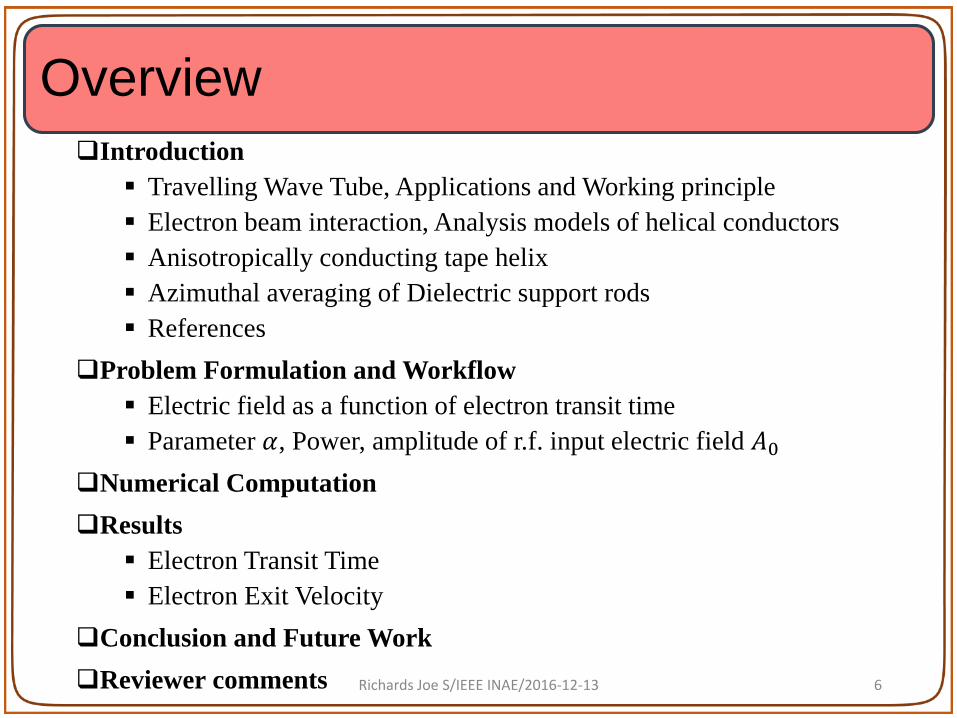
OverviewIntroduction
Travelling Wave Tube, Applications and Working principle Electron beam interaction, Analysis models of helical conductors Anisotropically conducting tape helix Azimuthal averaging of Dielectric support rods References
Problem Formulation and Workflow Electric field as a function of electron transit time Parameter 𝛼𝛼, Power, amplitude of r.f. input electric field 𝐴𝐴0
Numerical ComputationResults
Electron Transit Time Electron Exit Velocity
Conclusion and Future WorkReviewer comments Richards Joe S/IEEE INAE/2016-12-13 6
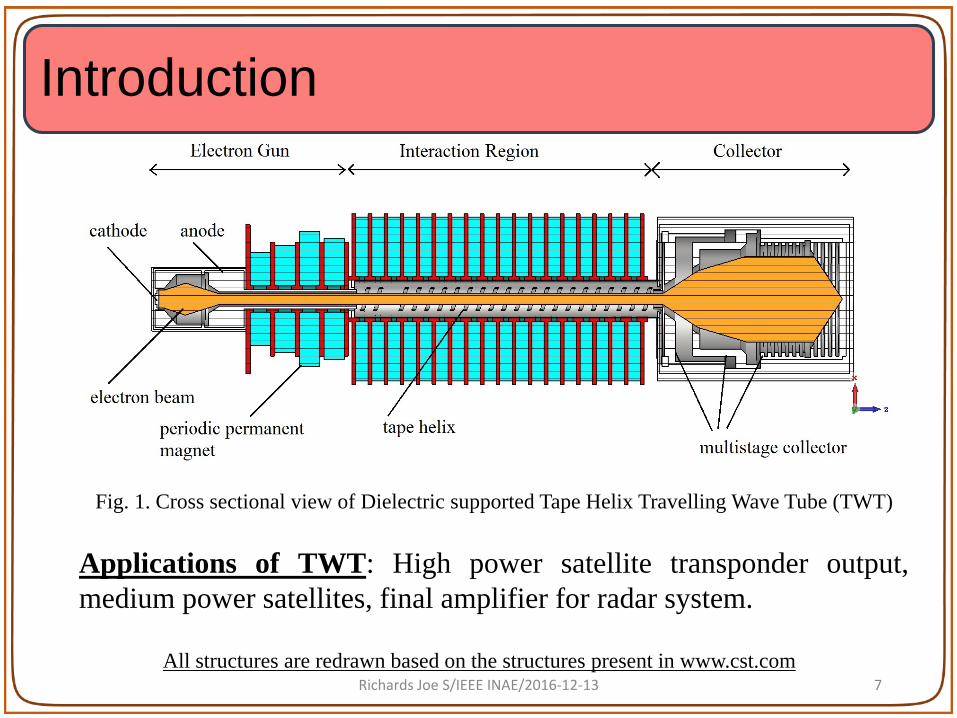
Fig. 1. Cross sectional view of Dielectric supported Tape Helix Travelling Wave Tube (TWT)
Introduction
All structures are redrawn based on the structures present in www.cst.com
Applications of TWT: High power satellite transponder output,medium power satellites, final amplifier for radar system.
Richards Joe S/IEEE INAE/2016-12-13 7

Working Principle of Helical TWT
Fig. 2. Cross sectional (y-z plane) view of interaction region of the slow wave structure
Generation of Electron beam
RF input given in Helix
Interaction of RF Signal with electron beam
Electron Bunches <=>Amplification of RF Signal
Amplified RF Signal received at output terminal
Richards Joe S/IEEE INAE/2016-12-13 8
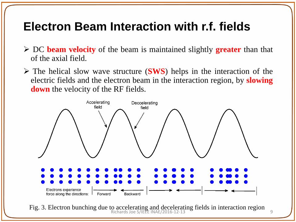
Electron Beam Interaction with r.f. fields
DC beam velocity of the beam is maintained slightly greater than thatof the axial field.
The helical slow wave structure (SWS) helps in the interaction of theelectric fields and the electron beam in the interaction region, by slowingdown the velocity of the RF fields.
Fig. 3. Electron bunching due to accelerating and decelerating fields in interaction regionRichards Joe S/IEEE INAE/2016-12-13 9
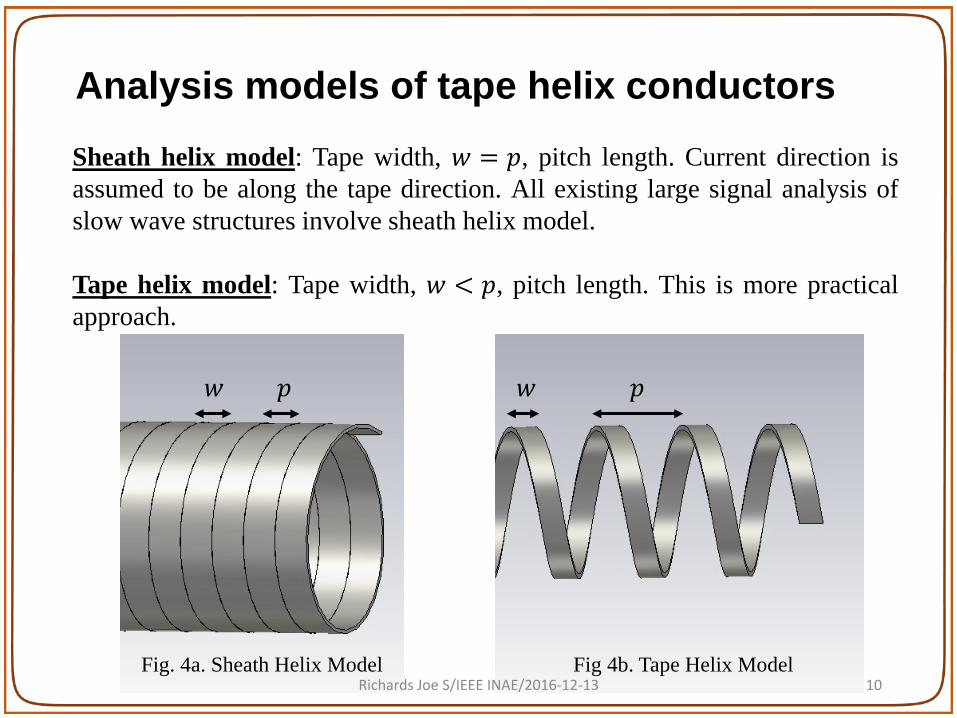
Sheath helix model: Tape width, 𝑤𝑤 = 𝑝𝑝, pitch length. Current direction isassumed to be along the tape direction. All existing large signal analysis ofslow wave structures involve sheath helix model.
Tape helix model: Tape width, 𝑤𝑤 < 𝑝𝑝, pitch length. This is more practicalapproach.
Analysis models of tape helix conductors
Fig 4b. Tape Helix Model
𝑤𝑤 𝑝𝑝
Fig. 4a. Sheath Helix Model
𝑤𝑤 𝑝𝑝
Richards Joe S/IEEE INAE/2016-12-13 10
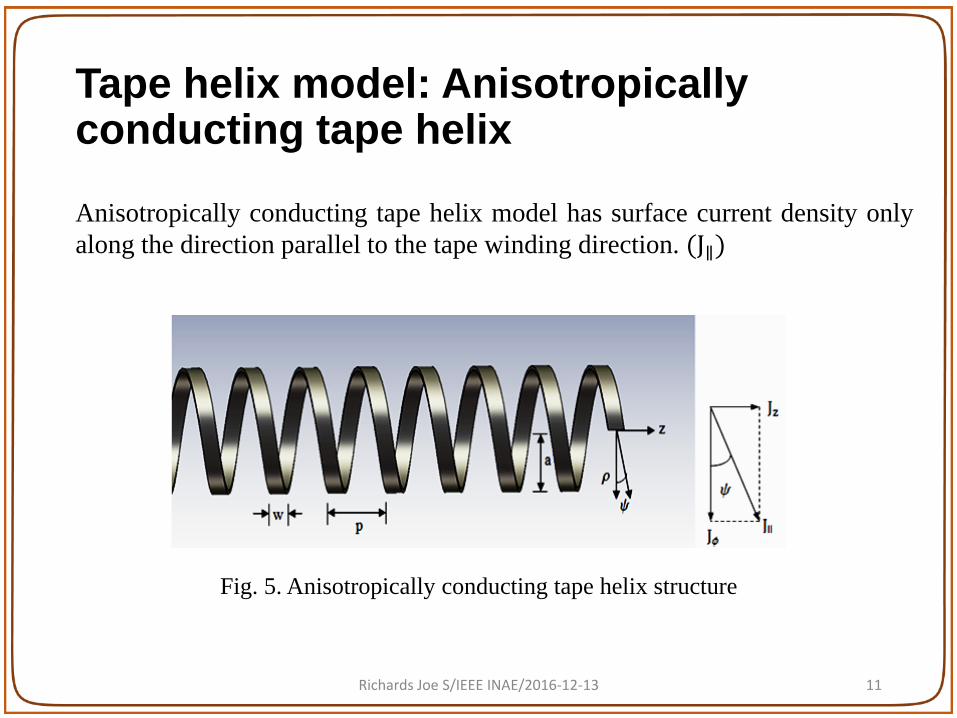
Tape helix model: Anisotropicallyconducting tape helix
Anisotropically conducting tape helix model has surface current density onlyalong the direction parallel to the tape winding direction. (J∥)
Fig. 5. Anisotropically conducting tape helix structure
Richards Joe S/IEEE INAE/2016-12-13 11
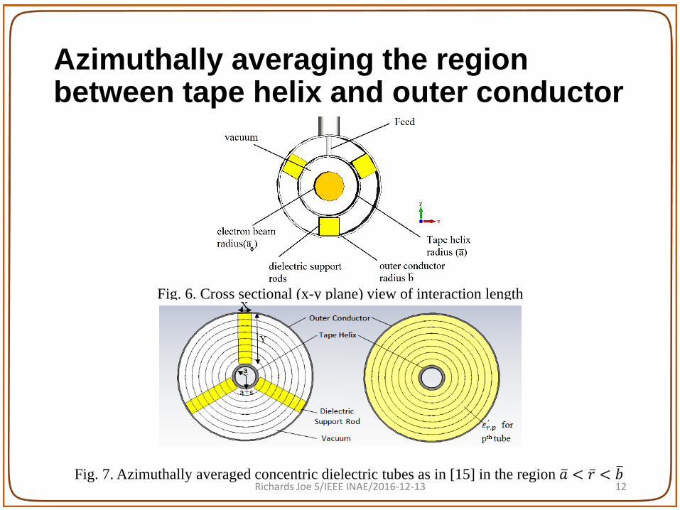
Fig. 6. Cross sectional (x-y plane) view of interaction length
Azimuthally averaging the region between tape helix and outer conductor
Fig. 7. Azimuthally averaged concentric dielectric tubes as in [15] in the region �𝑎𝑎 < ��𝑟 < �𝑏𝑏Richards Joe S/IEEE INAE/2016-12-13 12
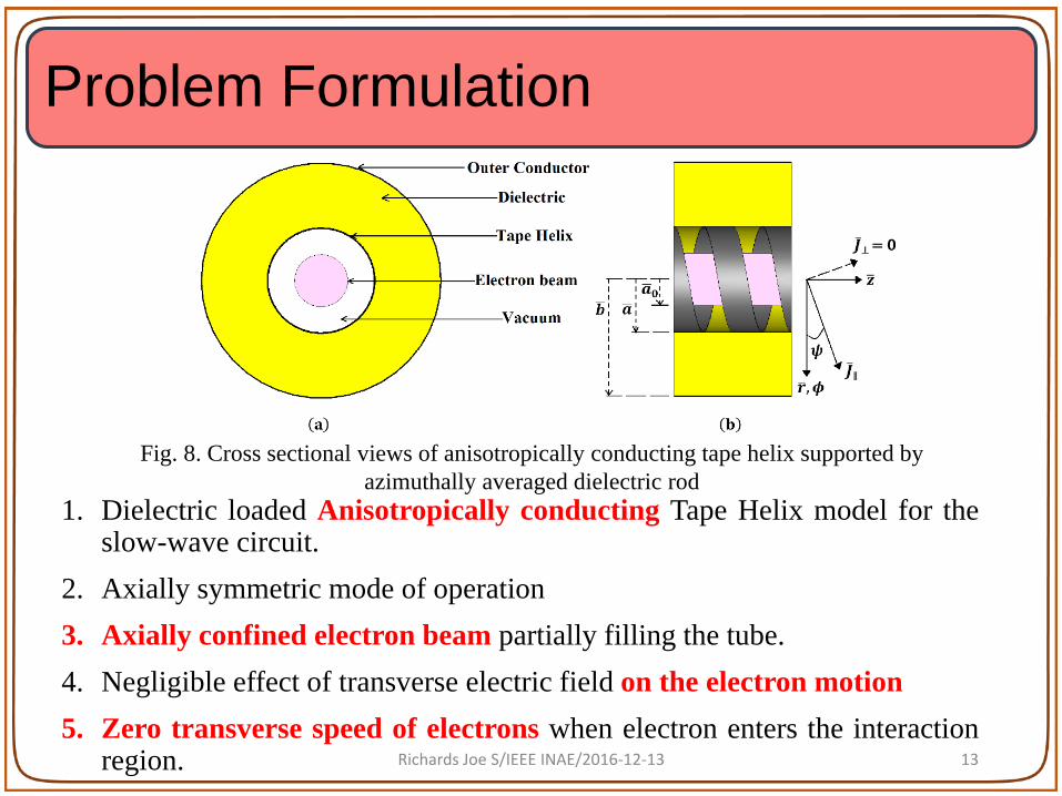
Problem Formulation
1. Dielectric loaded Anisotropically conducting Tape Helix model for theslow-wave circuit.
2. Axially symmetric mode of operation3. Axially confined electron beam partially filling the tube.4. Negligible effect of transverse electric field on the electron motion5. Zero transverse speed of electrons when electron enters the interaction
region.
Fig. 8. Cross sectional views of anisotropically conducting tape helix supported by azimuthally averaged dielectric rod
Richards Joe S/IEEE INAE/2016-12-13 13
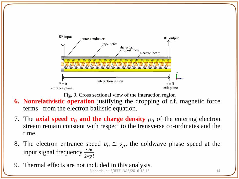
6. Nonrelativistic operation justifying the dropping of r.f. magnetic forceterms from the electron ballistic equation.
7. The axial speed 𝒗𝒗𝟎𝟎 and the charge density 𝜌𝜌0 of the entering electronstream remain constant with respect to the transverse co-ordinates and thetime.
8. The electron entrance speed 𝑣𝑣0 ≅ 𝑣𝑣𝑝𝑝, the coldwave phase speed at theinput signal frequency 𝜔𝜔0
2∗𝑝𝑝𝑝𝑝
9. Thermal effects are not included in this analysis.
Fig. 9. Cross sectional view of the interaction region
Richards Joe S/IEEE INAE/2016-12-13 14
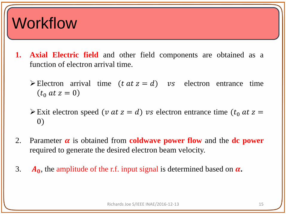
1. Axial Electric field and other field components are obtained as afunction of electron arrival time.
Electron arrival time (𝑡𝑡 𝑎𝑎𝑡𝑡 𝑧𝑧 = 𝑑𝑑) 𝑣𝑣𝑣𝑣 electron entrance time𝑡𝑡0 𝑎𝑎𝑡𝑡 𝑧𝑧 = 0
Exit electron speed (𝑣𝑣 𝑎𝑎𝑡𝑡 𝑧𝑧 = 𝑑𝑑) 𝑣𝑣𝑣𝑣 electron entrance time (𝑡𝑡0 𝑎𝑎𝑡𝑡 𝑧𝑧 =0)
2. Parameter 𝜶𝜶 is obtained from coldwave power flow and the dc powerrequired to generate the desired electron beam velocity.
3. 𝑨𝑨𝟎𝟎, the amplitude of the r.f. input signal is determined based on 𝜶𝜶.
Workflow
Richards Joe S/IEEE INAE/2016-12-13 15

Variables rendered dimensionless
Axial electron speed,
Fig. 8. Cross sectional views of anisotropically conducting tape helix supported by azimuthally averaged dielectric rod
Pitch angle, 𝜓𝜓 = 10°
Richards Joe S/IEEE INAE/2016-12-13 16
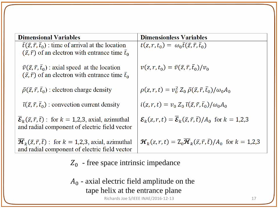
𝑍𝑍0 - free space intrinsic impedance
𝐴𝐴0 - axial electric field amplitude on thetape helix at the entrance plane
Richards Joe S/IEEE INAE/2016-12-13 17

Fourier series expansion of current density and charge density• 𝑞𝑞0(= 𝑣𝑣02𝜌𝜌0𝑍𝑍0/𝜔𝜔0𝐴𝐴0) corresponds to both the dimensionless
convection current density and the charge density at the entranceplane, 𝑧𝑧 = 0.
• 𝑡𝑡0𝑙𝑙 corresponds to the entrance time of the 𝑙𝑙𝑡𝑡𝑡 electron whichcontributes to the time of arrival at (𝑧𝑧, 𝑟𝑟) location at time 𝑡𝑡.
• The current density and the charge density terms are then expandedin Fourier series
Richards Joe S/IEEE INAE/2016-12-13 18

Fourier coefficients are expanded in terms of the contribution of every electron’s electron arrival time
Richards Joe S/IEEE INAE/2016-12-13 19
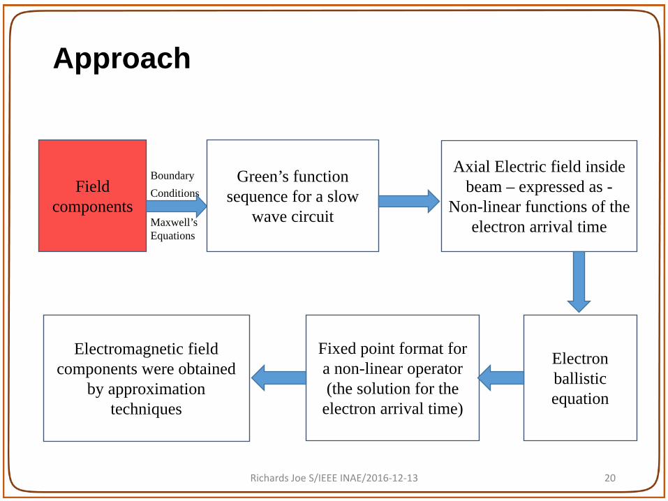
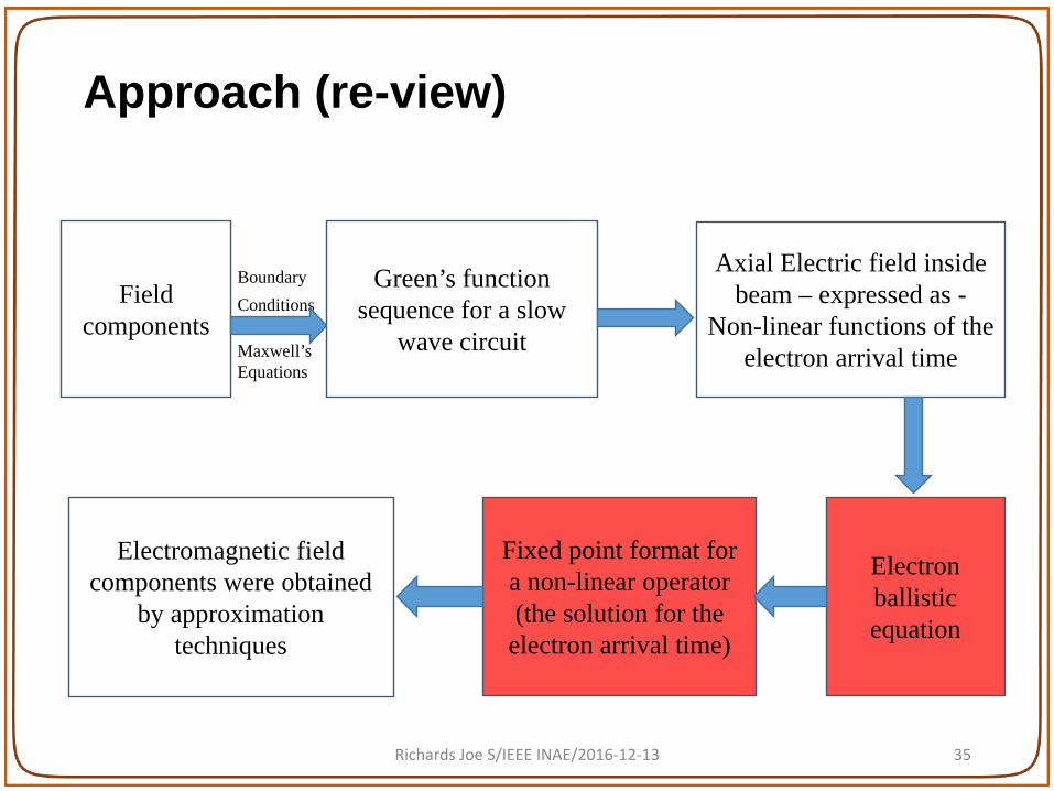
Approach
Field components
Green’s function sequence for a slow
wave circuit
Axial Electric field inside beam – expressed as -
Non-linear functions of the electron arrival time
Electron ballistic equation
Fixed point format for a non-linear operator (the solution for the
electron arrival time)
Electromagnetic field components were obtained
by approximation techniques
Boundary Conditions
Maxwell’s Equations
Richards Joe S/IEEE INAE/2016-12-13 20
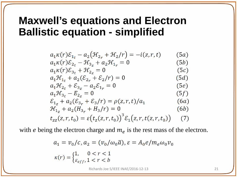
Maxwell’s equations and Electron Ballistic equation - simplified
with 𝑒𝑒 being the electron charge and 𝑚𝑚𝑒𝑒 is the rest mass of the electron.
Richards Joe S/IEEE INAE/2016-12-13 21

In the entrance plane of the interaction region, 𝑧𝑧 = 0,
The monochromatic signaling conditions at the tape helix in the entrance plane, with the phase factor, 𝐴𝐴(≜ exp 𝑗𝑗𝑗𝑗 ), in the entrance plane is
Along the boundary of the electron beam radius, 𝒓𝒓 = 𝒂𝒂, the continuity of the electric and magnetic field components are
Boundary conditions
Richards Joe S/IEEE INAE/2016-12-13 22
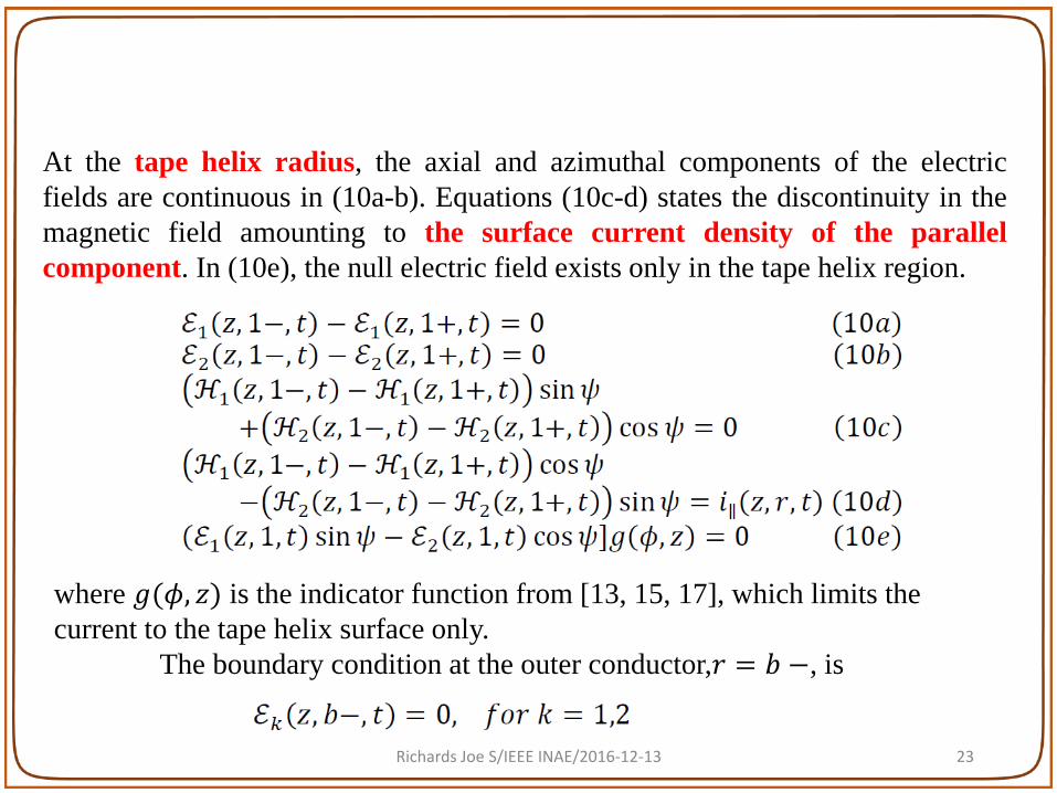
At the tape helix radius, the axial and azimuthal components of the electricfields are continuous in (10a-b). Equations (10c-d) states the discontinuity in themagnetic field amounting to the surface current density of the parallelcomponent. In (10e), the null electric field exists only in the tape helix region.
where 𝑔𝑔(𝜙𝜙, 𝑧𝑧) is the indicator function from [13, 15, 17], which limits the current to the tape helix surface only.
The boundary condition at the outer conductor,𝑟𝑟 = 𝑏𝑏 −, is
Richards Joe S/IEEE INAE/2016-12-13 23

Approach (re-view)
Field components
Green’s function sequence for a slow
wave circuit
Axial Electric field inside beam – expressed as -
Non-linear functions of the electron arrival time
Electron ballistic equation
Fixed point format for a non-linear operator (the solution for the
electron arrival time)
Electromagnetic field components were obtained
by approximation techniques
Boundary Conditions
Maxwell’s Equations
Richards Joe S/IEEE INAE/2016-12-13 24
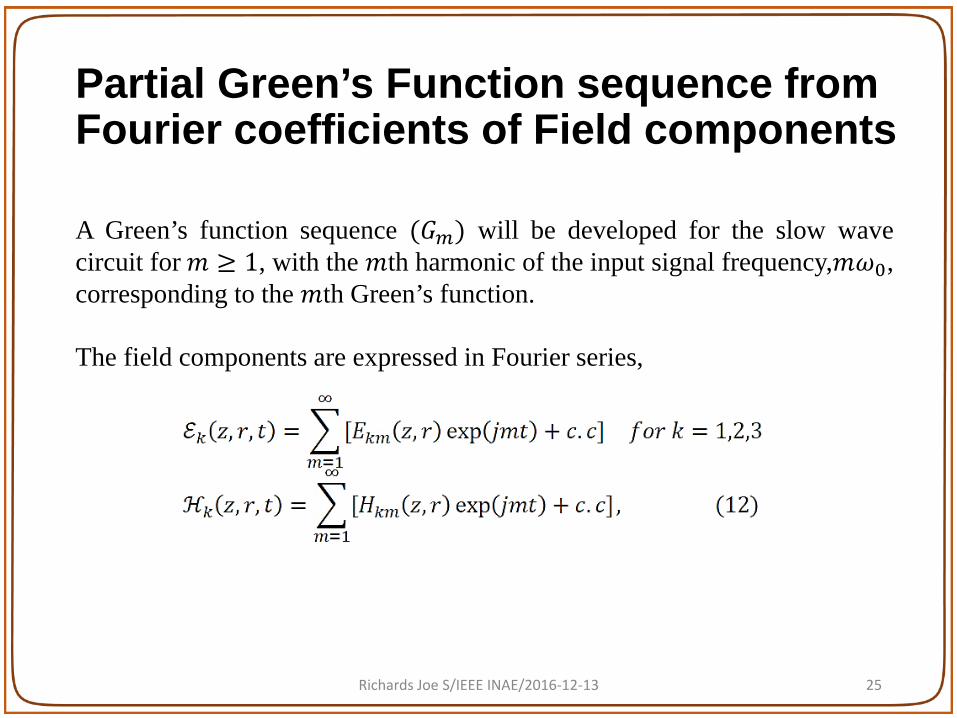
Partial Green’s Function sequence from Fourier coefficients of Field components
A Green’s function sequence (𝐺𝐺𝑚𝑚) will be developed for the slow wavecircuit for𝑚𝑚 ≥ 1, with the 𝑚𝑚th harmonic of the input signal frequency,𝑚𝑚𝜔𝜔0,corresponding to the 𝑚𝑚th Green’s function.
The field components are expressed in Fourier series,
Richards Joe S/IEEE INAE/2016-12-13 25
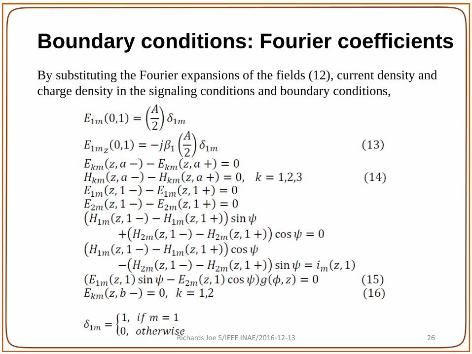
Boundary conditions: Fourier coefficientsBy substituting the Fourier expansions of the fields (12), current density and charge density in the signaling conditions and boundary conditions,
Richards Joe S/IEEE INAE/2016-12-13 26

As in [8, 11], the substitution of Fourier coefficients of the fields into theMaxwell’s equations (5-6) are also carried out.Then the non-homogeneous term 𝑖𝑖𝑚𝑚(𝑧𝑧, 𝑟𝑟) is represented as a function of theaxial components bounded by the interval [0,d]
where
Richards Joe S/IEEE INAE/2016-12-13 27
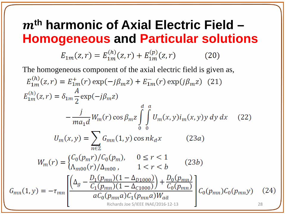
𝒎𝒎th harmonic of Axial Electric Field –Homogeneous and Particular solutions
The homogeneous component of the axial electric field is given as,
Richards Joe S/IEEE INAE/2016-12-13 28
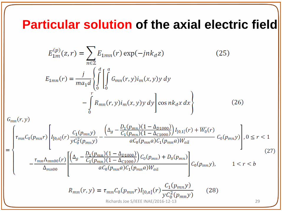
Particular solution of the axial electric field
Richards Joe S/IEEE INAE/2016-12-13 29
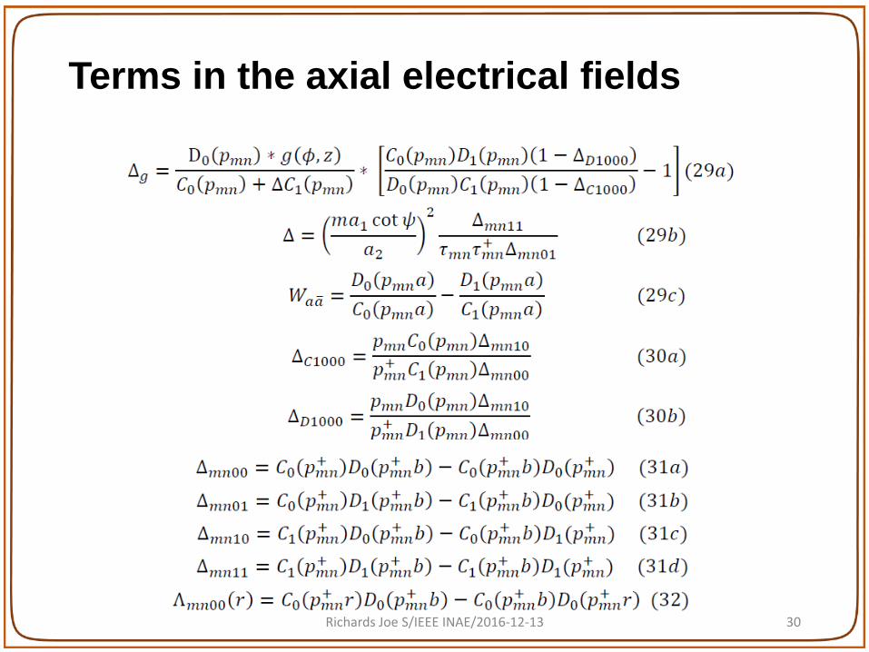
Terms in the axial electrical fields
Richards Joe S/IEEE INAE/2016-12-13 30

where, 𝐶𝐶𝑣𝑣 and 𝐷𝐷𝑣𝑣 are common symbols for the Bessel’s functions andmodified Bessel’s functions for first kind and second kind
Richards Joe S/IEEE INAE/2016-12-13 31
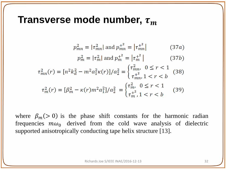
Transverse mode number, 𝝉𝝉𝒎𝒎
where 𝛽𝛽𝑚𝑚 > 0 is the phase shift constants for the harmonic radianfrequencies 𝑚𝑚𝜔𝜔0 derived from the cold wave analysis of dielectricsupported anisotropically conducting tape helix structure [13].
Richards Joe S/IEEE INAE/2016-12-13 32

Approach (re-view)
Field components
Green’s function sequence for a slow
wave circuit
Axial Electric field inside beam – expressed as -
Non-linear functions of the electron arrival time
Electron ballistic equation
Fixed point format for a non-linear operator (the solution for the
electron arrival time)
Electromagnetic field components were obtained
by approximation techniques
Boundary Conditions
Maxwell’s Equations
Richards Joe S/IEEE INAE/2016-12-13 33
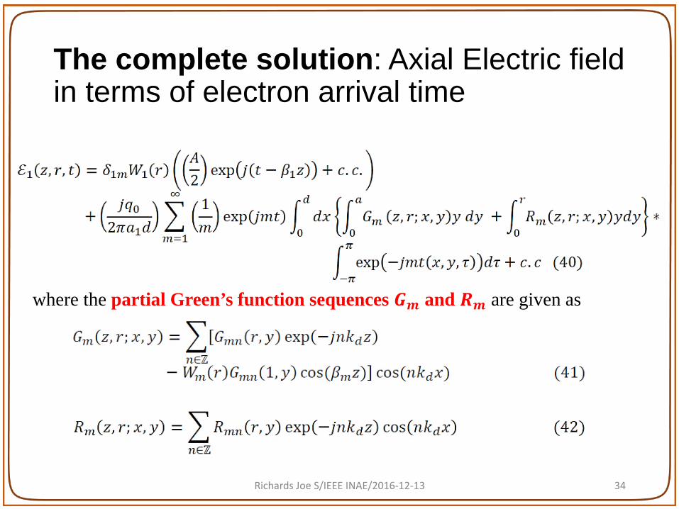
The complete solution: Axial Electric field in terms of electron arrival time
where the partial Green’s function sequences 𝑮𝑮𝒎𝒎 and 𝑹𝑹𝒎𝒎 are given as
Richards Joe S/IEEE INAE/2016-12-13 34
Approach (re-view)
Field components
Green’s function sequence for a slow
wave circuit
Axial Electric field inside beam – expressed as -
Non-linear functions of the electron arrival time
Electron ballistic equation
Fixed point format for a non-linear operator (the solution for the
electron arrival time)
Electromagnetic field components were obtained
by approximation techniques
Boundary Conditions
Maxwell’s Equations
Richards Joe S/IEEE INAE/2016-12-13 35
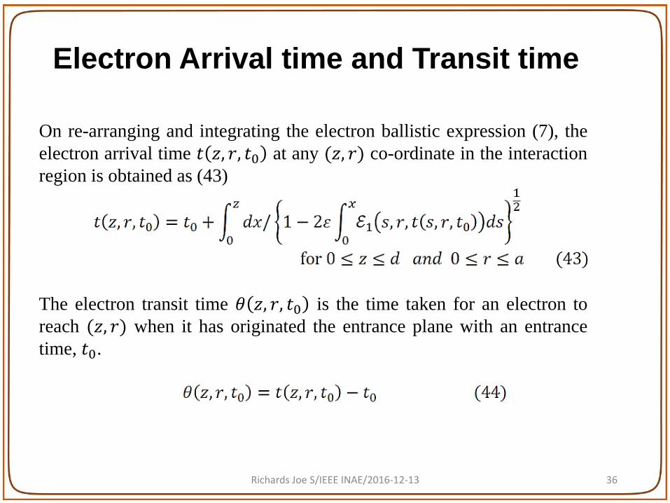
Electron Arrival time and Transit time
On re-arranging and integrating the electron ballistic expression (7), theelectron arrival time 𝑡𝑡 𝑧𝑧, 𝑟𝑟, 𝑡𝑡0 at any (𝑧𝑧, 𝑟𝑟) co-ordinate in the interactionregion is obtained as (43)
The electron transit time 𝑗𝑗 𝑧𝑧, 𝑟𝑟, 𝑡𝑡0 is the time taken for an electron toreach (𝑧𝑧, 𝑟𝑟) when it has originated the entrance plane with an entrancetime, 𝑡𝑡0.
Richards Joe S/IEEE INAE/2016-12-13 36

Cold wave power and input DC power
The electron beam current of 𝐼𝐼0 amps and the anode voltage 𝑉𝑉0 are computedaccelerate the electrons from zero initial velocity at cathode to the requiredelectron beam velocity 𝑣𝑣0 at the interaction region’s entrance plane (𝑧𝑧, 𝑟𝑟). Thisamounts to the DC power, 𝑃𝑃𝑑𝑑𝑑𝑑. The cold wave power propagating forward atthe signal frequency 𝜔𝜔0 is represented as 𝑃𝑃𝑝𝑝𝑖𝑖[9, 12], where
with 𝑃𝑃11 being the dimensionless power computed from the cold wave fieldsfrom [13, 14] and 𝑌𝑌0 is the free-space admittance (inverse of free spaceimpedance,𝑍𝑍0 = 120𝜋𝜋).
The factor 𝛼𝛼 in (46) provides the amplitude of the r.f. signal 𝐴𝐴0 to be chosenfor the intended level of signal amplification as in [9, 12].
Richards Joe S/IEEE INAE/2016-12-13 37

Approach (re-view)
Field components
Green’s function sequence for a slow
wave circuit
Axial Electric field inside beam – expressed as -
Non-linear functions of the electron arrival time
Electron ballistic equation
Fixed point format for a non-linear operator (the solution for the
electron arrival time)
Electromagnetic field components were obtained
by approximation techniques
Boundary Conditions
Maxwell’s Equations
Richards Joe S/IEEE INAE/2016-12-13 38
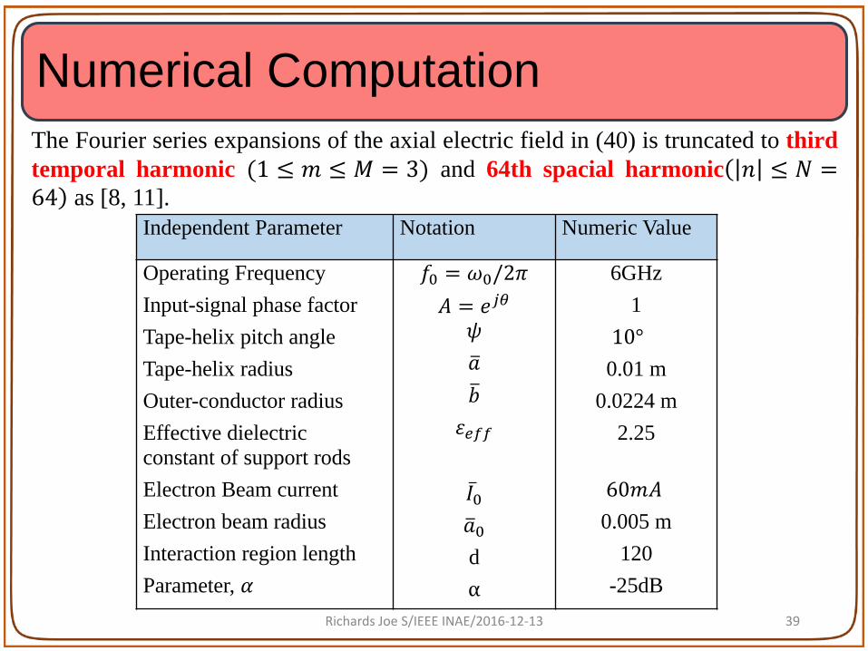
Independent Parameter Notation Numeric Value
Operating Frequency Input-signal phase factorTape-helix pitch angleTape-helix radiusOuter-conductor radiusEffective dielectric constant of support rods Electron Beam currentElectron beam radiusInteraction region lengthParameter, 𝛼𝛼
𝑓𝑓0 = 𝜔𝜔0/2𝜋𝜋𝐴𝐴 = 𝑒𝑒𝑗𝑗𝑗𝑗
𝜓𝜓�𝑎𝑎�𝑏𝑏
𝜀𝜀𝑒𝑒𝑒𝑒𝑒𝑒
𝐼𝐼0�𝑎𝑎0dα
6GHz1
10°0.01 m
0.0224 m2.25
60𝑚𝑚𝐴𝐴0.005 m
120-25dB
Numerical ComputationThe Fourier series expansions of the axial electric field in (40) is truncated to thirdtemporal harmonic (1 ≤ 𝑚𝑚 ≤ 𝑀𝑀 = 3) and 64th spacial harmonic(
)𝑛𝑛 ≤ 𝑁𝑁 =
64 as [8, 11].
Richards Joe S/IEEE INAE/2016-12-13 39
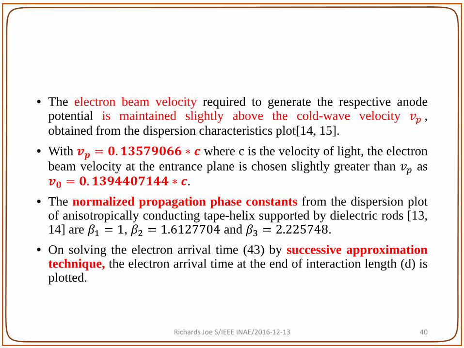
• The electron beam velocity required to generate the respective anodepotential is maintained slightly above the cold-wave velocity 𝑣𝑣𝑝𝑝 ,obtained from the dispersion characteristics plot[14, 15].
• With 𝒗𝒗𝒑𝒑 = 𝟎𝟎.𝟏𝟏𝟏𝟏𝟏𝟏𝟏𝟏𝟏𝟏𝟎𝟎𝟏𝟏𝟏𝟏 ∗ 𝒄𝒄 where c is the velocity of light, the electronbeam velocity at the entrance plane is chosen slightly greater than 𝑣𝑣𝑝𝑝 as𝒗𝒗𝟎𝟎 = 𝟎𝟎.𝟏𝟏𝟏𝟏𝟏𝟏𝟏𝟏𝟏𝟏𝟎𝟎𝟏𝟏𝟏𝟏𝟏𝟏𝟏𝟏 ∗ 𝒄𝒄.
• The normalized propagation phase constants from the dispersion plotof anisotropically conducting tape-helix supported by dielectric rods [13,14] are 𝛽𝛽1 = 1, 𝛽𝛽2 = 1.6127704 and 𝛽𝛽3 = 2.225748.
• On solving the electron arrival time (43) by successive approximationtechnique, the electron arrival time at the end of interaction length (d) isplotted.
Richards Joe S/IEEE INAE/2016-12-13 40

Electron Transit Time
The media below displays an example of electrons entering atentrance plane 𝑧𝑧 = 0 with different entrance times, takedifferent transit times to reach the exit plane 𝑧𝑧 = 𝑑𝑑.
2 1
Fig. 9 The electrons arriving at different entrance times, travel at different velocities toreach the exit plane at different arrival times
Richards Joe S/IEEE INAE/2016-12-13 41
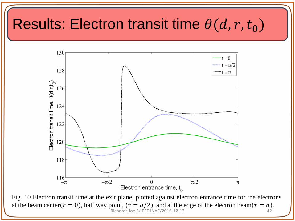
Results: Electron transit time 𝑗𝑗(𝑑𝑑, 𝑟𝑟, 𝑡𝑡0)
Fig. 10 Electron transit time at the exit plane, plotted against electron entrance time for the electronsat the beam center(𝑟𝑟 = 0), half way point, (𝑟𝑟 = 𝑎𝑎/2) and at the edge of the electron beam(𝑟𝑟 = 𝑎𝑎).
Richards Joe S/IEEE INAE/2016-12-13 42
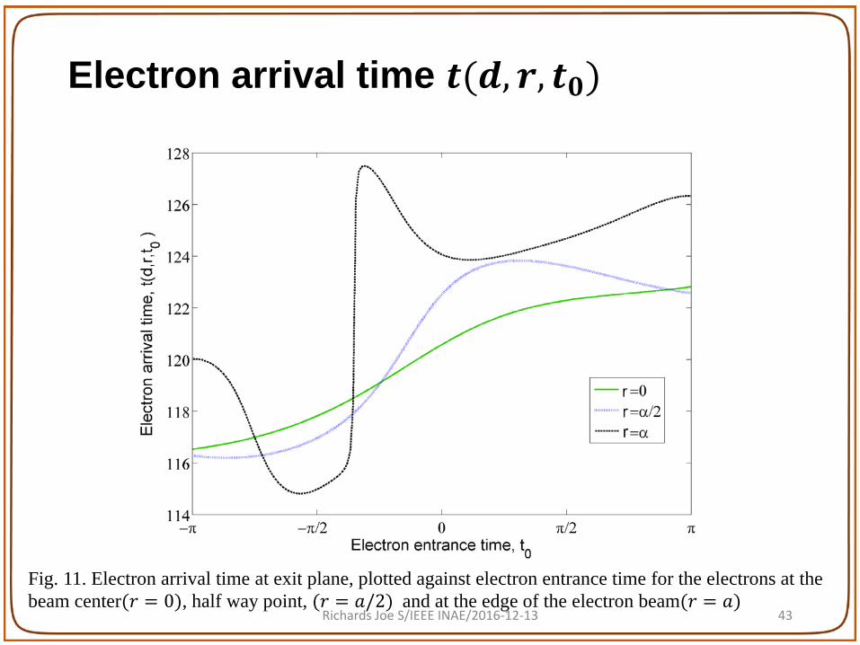
Electron arrival time 𝒕𝒕(𝒅𝒅, 𝒓𝒓, 𝒕𝒕𝟎𝟎)
Fig. 11. Electron arrival time at exit plane, plotted against electron entrance time for the electrons at the beam center(𝑟𝑟 = 0), half way point, (𝑟𝑟 = 𝑎𝑎/2) and at the edge of the electron beam(𝑟𝑟 = 𝑎𝑎)
Richards Joe S/IEEE INAE/2016-12-13 43
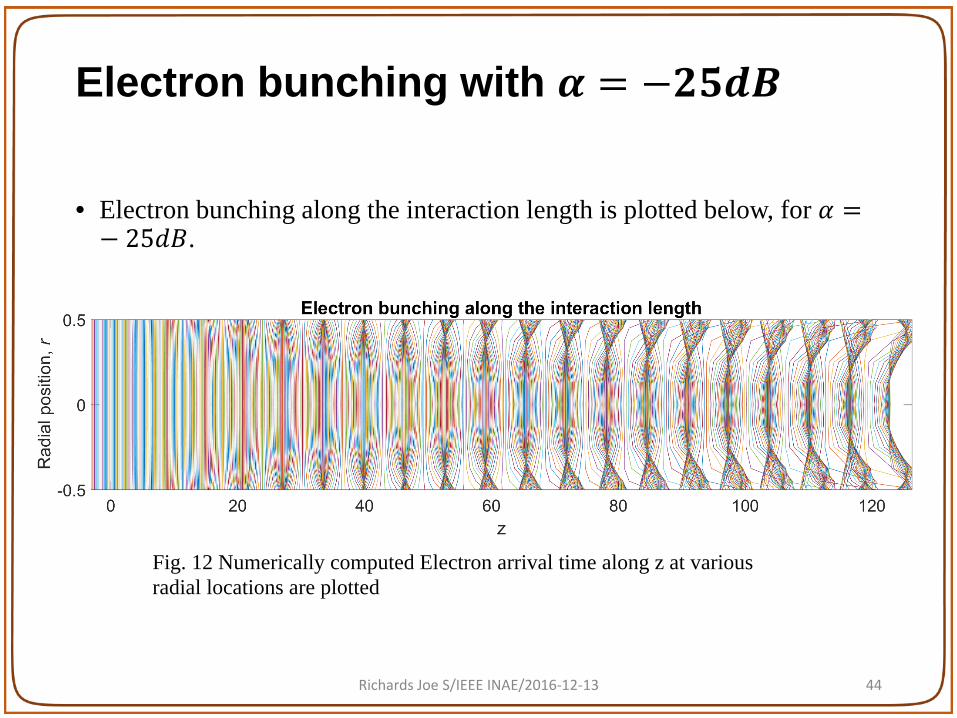
Electron bunching with 𝜶𝜶 = −𝟐𝟐𝟏𝟏𝒅𝒅𝟐𝟐
• Electron bunching along the interaction length is plotted below, for 𝛼𝛼 =− 25𝑑𝑑𝑑𝑑.
Fig. 12 Numerically computed Electron arrival time along z at various radial locations are plotted
Richards Joe S/IEEE INAE/2016-12-13 44
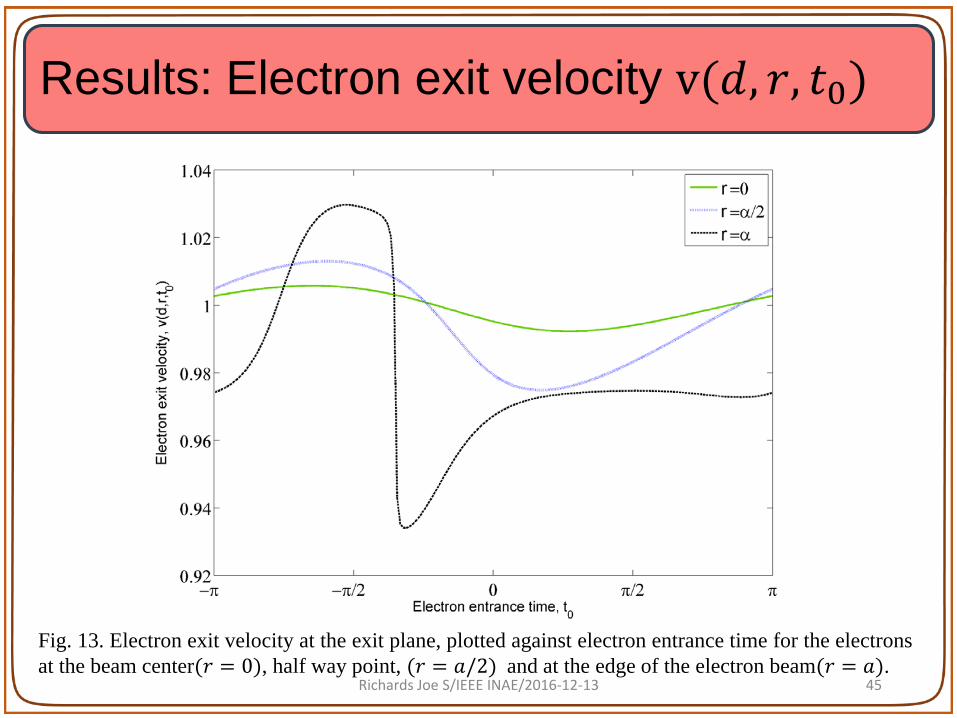
Results: Electron exit velocity v(𝑑𝑑, 𝑟𝑟, 𝑡𝑡0)
Fig. 13. Electron exit velocity at the exit plane, plotted against electron entrance time for the electronsat the beam center(𝑟𝑟 = 0), half way point, (𝑟𝑟 = 𝑎𝑎/2) and at the edge of the electron beam(𝑟𝑟 = 𝑎𝑎).
Richards Joe S/IEEE INAE/2016-12-13 45

A rigorous large signal field analysis was performed on thepractical case of linear beam travelling wave tube with tapehelix slow wave structure supported by dielectric rods.
The transit time and the exit velocity at the exit plane of theinteraction region were computed and plotted.
The numerical computation of the axial electric field,current gain, power gain and the conversion efficiency arein progress.
In the future, the large signal field analysis will be performedin a 3D simulation software.
Conclusion and Future Work
Richards Joe S/IEEE INAE/2016-12-13 46

The manuscript presents the computation of the electron transit time andthe electron exit velocity in a dielectric supported helix traveling wave tubeamplifiers (TWTA) by solving the non-homogeneous boundary valueproblem. The following suggestion can be incorporated to bring out thenovelty of the presented work.1. The large signal analysis results of tape helix model analyzed in this
paper could be compared with the results obtained from the existinganalysis of sheath helix model.Since the numerical computations include rigorous field analysis, the
analysis results of sheath helix model could not completed in the shortduration of time. However, the suggestion will be considered for the futureworks.2. Maintain consistency in referencing symbols throughout the manuscript
The notations of variables were updated and corrected in thepresentation.
Reviewer Comments
Richards Joe S/IEEE INAE/2016-12-13 47

SummaryIntroduction
Travelling Wave Tube, Applications and Working principle Electron beam interaction, Analysis models of helical conductors Anisotropically conducting tape helix Azimuthal averaging of Dielectric support rods References
Problem Formulation and Workflow Electric field as a function of electron transit time Parameter 𝛼𝛼, Power, amplitude of r.f. input electric field 𝐴𝐴0
Numerical ComputationResults
Electron Transit Time Electron Exit Velocity
Conclusion and Future WorkReviewer comments Richards Joe S/IEEE INAE/2016-12-13 48
References1. J. R. Pierce and L. M. Field, "Traveling-Wave Tubes," in Proceedings of the
IRE, vol. 35, no. 2, pp. 108-111, Feb. 1947.
2. J. R. Pierce, "Theory of the Beam-Type Traveling-Wave Tube," in Proceedingsof the IRE, vol. 35, no. 2, pp. 111-123, Feb. 1947.
3. R. Kompfner, "The Traveling-Wave Tube as Amplifier at Microwaves," inProceedings of the IRE, vol. 35, no. 2, pp. 124-127, Feb. 1947.
4. L. J. Chu and J. D. Jackson, "Field Theory of Traveling-Wave Tubes," inProceedings of the IRE, vol. 36, no. 7, pp. 853-863, July 1948.
5. Robert E. Collin, “Foundations for Microwave Engineering” , 2, Wiley-IEEEPress, 2005.
6. N. R. Vanderplaats, M. A. Kodis and H. P. Freund, "Design of traveling wavetubes based on field theory," in IEEE Transactions on Electron Devices, vol. 41,no. 7, pp. 1288-1296, Jul 1994.
Richards Joe S/IEEE INAE/2016-12-13 49
7. H. P. Freund, E. G. Zaidman, M. A. Kodis and N. R. Vanderplaats,"Linearized field theory of a dielectric-loaded helix traveling wave tubeamplifier," in IEEE Transactions on Plasma Science, vol. 24, no. 3, pp.895-904, Jun 1996.
8. N. Kalyanasundaram, "Large-signal field analysis of an O-typetravelling-wave amplifier. Part 1: theory," in IEE Proceedings I - Solid-State and Electron Devices, vol. 131, no. 5, pp. 145-152, October 1984.
9. N. Kalyanasundaram and R. Chinnadurai, "Large-signal field analysisof an O-type travelling wave amplifier. Part 2: Numerical results," inIEE Proceedings I - Solid-State and Electron Devices, vol. 133, no. 4,pp. 163-168, August 1986.
10.N. Kalyanasundaram and R. Chinnadurai, "Large-signal field analysisof an O-type travelling wave amplifier. Part 3: Three-dimensionalelectron motion," in IEE Proceedings I - Solid-State and ElectronDevices, vol. 135, no. 3, pp. 59-66, June 1988.
Richards Joe S/IEEE INAE/2016-12-13 50
11.N. Kalyanasundaram and A. Agnihotri, "Large-signal field analysis of alinear beam traveling wave amplifier for a sheath-helix model of the slow-wave structure supported by dielectric rods. part 1: theory," Progress InElectromagnetics Research B, Vol. 57, pp. 87-104, 2014.
12.N. Kalyanasundaram and A. Agnihotri, "Large signal field analysis of alinear beam traveling wave amplifier for a sheath-helix model of the slow-wave structure supported by dielectric rods. part 2: neumerical results,"Progress In Electromagnetics Research B, Vol. 57, pp. 105-114, 2014.
13.N. Kalyanasundaram and G. N. Babu, "Propagation of electromagneticwaves guided by the anisotropically conducting model of a tape helixsupported by dielectric rods," Progress In Electromagnetics Research B,Vol. 51, 81-99, 2013.
14.G. N. Babu, R. J. Stanislaus and S. Joshi, "Wave propagationcharacteristics in anisotropically conducting dielectric loaded tape helixslow wave structures," Vacuum Electronics Conference, IEEEInternational, Monterey, CA, 2014, pp. 327-328
Richards Joe S/IEEE INAE/2016-12-13 51
15.P. K. Jain and B. N. Basu, "The inhomogeneous loading effects ofpractical dielectric supports for the helical slow-wave structure of aTWT," in IEEE Transactions on Electron Devices, vol. 34, no. 12, pp.2643-2648, Dec 1987.
16.G. Naveen Babu and R. J. Stanislaus, "Propagation of electromagneticwaves guided by perfectly conducting model of a tape helix supportedby dielectric rods," in IET Microwaves, Antennas & Propagation, vol.10, no. 6, pp. 676-685, 4 24 2016.
17.N. Kalyanasundaram and G. N. Babu, "Perfectly conducting tape-helixmodel for guided electromagnetic wave propagation," in IETMicrowaves, Antennas & Propagation, vol. 6, no. 8, pp. 899-907, June 72012.
Richards Joe S/IEEE INAE/2016-12-13 52

Richards Joe S/IEEE INAE/2016-12-13 53