electron diffraction by carbon nanotubes · 1department of physics, facultés universitaires...
TRANSCRIPT

Electron diffraction by carbon nanotubes
415
Scanning Microscopy Vol. 12, No. 3, 1998 (Pages 415-436) 0891-7035/98$5.00+.25Scanning Microscopy International, Chicago (AMF O’Hare), IL 60666 USA
ELECTRON DIFFRACTION BY CARBON NANOTUBES
Abstract
This paper first presents results from electrondiffraction (ED) and transmission electron microscopy (TEM)of carbon nanotubes. TEM and ED of straight or coilednanotubes are shown and the mechanisms of formation of thediffraction patterns caused by their specific atomic structuresare qualitatively explained. Then a quantitative theory ofkinematical diffraction by straight carbon nanotubes isproposed. The formalism is inspired from the theory of X-Raydiffraction by helical structures originally developed byCochran, Crick and Vand for biological molecules. Each of thecylindrical graphene layers in a nanotube is viewed as beingconstructed from a finite set of regularly spaced carbon helicessharing the nanotube axis. This description leads to an exact,compact formula for the total kinematical diffraction amplitudeof a complete monolayer tubule of arbitrary chirality. Weillustrate the theory with computer simulations of the diffractionpatterns of monolayer tubules and multilayer nanotubes ofmixed chiralities and compare with observed ED patterns. Theclosed-form formula for the scattering amplitude of a singletubule also provides the molecular form factor to furthercompute the diffraction by the regular lattice of parallel tubulesobserved recently. We finally indicate briefly how the methodcan be extended to compute the kinematical diffraction bycoiled nanotubes and other helical structures of nanometersize.
Key Words: Carbon nanotubes, transmission electronmicroscopy, electron diffraction, helical structures.
*Address for correspondence:A.A. LucasFacultés Universitaires Notre-Dame de la Paixrue de Bruxelles 61B-5000 Namur, Belgium
Telephone number: + 32 81 72 47 08Fax number: + 32 81 72 47 07
E-mail: [email protected]
A.A. Lucas1*, V. Bruyninckx1, Ph. Lambin1, D. Bernaerts2, S. Amelinckx2, J. Van Landuyt2
and G. Van Tendeloo2
1Department of Physics, Facultés Universitaires Notre-Dame de la Paix, Namur, Belgium2EMAT, University of Antwerp (RUCA), Belgium
(Received for publication July 18, 1996 and in revised form January 28, 1997)
Introduction
It has been realized in the past ten years that pureelemental carbon can condense in a variety of new three-dimensional structures different from the traditional crystallinesp2 planar graphite and sp3 diamond. When a high-temperature carbon vapor cools down and condenses in aninert atmosphere (Kroto et al., 1985; Krätschmer et al., 1990)spheroidal, closed-cage carbon clusters called fullerenes areformed with predominantly sp2 bonding between the atoms,the most celebrated example being the truncated-icosahedronshaped C
60 molecule first identified by Kroto et al., (1985). In
addition to these globular fullerenes, other types of sp2 bondedclusters were discovered, in particular hollow carbon fibers ofmicrometer lengths and nanometer diameters. Iijima (1991) wasthe first to observe these tubular fullerenes in the electrodedeposit formed in the carbon-arc method of fullereneproduction (Krätschmer et al., 1990). Using transmissionElectron Diffraction (ED) and high-resolution TransmissionElectron Microscopy (TEM), he could demonstrate that thenanotubes consist of a few individual graphene sheets rolledup into coaxial circular cylinders of nanometer diameters andthat the seamless cylinders are separated by the canonicalgraphitic interlayer distance of about 3.4 Å. Ebbesen andAjayan (1992) succeeded in adjusting the conditions of thecarbon-arc evaporation to make nanotubes in large quantities.The nanotubes can be purified from undesirable sootcomponents by controlled oxidation (Ebbesen et al., 1994).Shortly after the discovery of the multilayer nanotubes, Iijimaand Ichihashi (1993) and Bethune et al., (1993) were able toproduce, in a carbon-arc generator, abundant amounts ofsingle-wall, or monolayer tubules by co-evaporating atransition metal (e.g., Fe or Co) along with carbon. Iijima andIchihashi (1993) managed to obtain ED and TEM pictures ofsuch a single-wall tubule. The reader is referred to Ebbesen(1994) for a review of nanotube (carbon-arc) synthesis andproperties.
Among the most detailed TEM and ED studies of themorphology of straight multilayer nanotubes are thosereported by Zhang et al. (1993a,b) and by Liu and Cowley(1994a,b). A few selected examples will be discussed.
A different approach to carbon nanotube synthesis isthe low-temperature, catalytic growth method which was used

416
A.A. Lucas et al.
by José-Yacaman et al. (1993) and by Ivanov et al. (1994).This method, which consists in the cracking of hydrocarbonson the surface of a finely divided metal catalyst, was alreadyin widespread use for the catalytic production of mesoscopiccarbon fibers (reviews of which are given by: Dresselhaus etal., 1988; Baker, 1989; Rodriguez, 1993). Ivanov et al. (1994)showed that in the appropriate synthesis conditions, besidesthe straight nanotubes, several weight percent of regularlycoiled nanotubes were co-synthesized by the catalyst. Apartfrom their size, the coiled nanotubes appear to be similar tothe coiled carbon filaments of mesoscopic diameters previouslyobserved (see Kawaguchi et al., 1992, and references therein).TEM and ED studies (Ivanov et al., 1994; Zhang et al., 1994)have shown that, like globular fullerenes, the coiled as well asthe straight, catalytically grown nanotubes when properlyannealed and purified are hollow and have a degree ofgraphitization comparable to that of the carbon-arc grownspecies which makes them suitable for observation by high-resolution electron microscopy and diffraction.
A further method of nanotube synthesis is byelectrolysis (Hsu et al., 1995).
A number of papers have been devoted to the possiblegrowth mechanisms for straight or coiled nanotubes (Amelinckxet al., 1994, 1995b; Colbert et al., 1994; Gamaly and Ebbesen,1995; Fonseca et al., 1995; Guo et al., 1995a,b; Colbert andSmalley, 1995) but these will not be discussed here.
Nanotubes are of great interest for their novelstructural (Dresselhaus et al., 1992), electronic (Hamada etal., 1992; Mintmire et al.,, 1992; Charlier and Michenaud, 1993;Lambin et al., 1995; Langer et al., 1995), optical (Hiura et al.,1993; Bacsa and De Heer, 1995; Henrard et al., 1996), magnetic(Lu, 1995) and other properties. For practical applications, theyare expected to exhibit mechanical properties (Robertson etal., 1992) approaching the theoretical limit for sp2 bondedcarbon and could lead to composite materials superior instrength to those prepared with the macroscopic andmesoscopic carbon fibers in current industrial usage(Dresselhaus et al., 1988).
In the rest of this paper, we concentrate on the twotechniques best suited for ascertaining the structuralcharacteristics of a single nanotube, namely TEM and ED.We examine a few typical TEM and ED micrographs of straightor coiled nanotubes. We discuss qualitatively the mechanismsby which the micrographs are generated from the scatteringof electrons by the assumed atomic structure of the nanotubes.Then we present a mathematical theory for the calculation ofelectron scattering in the first Born, or kinematicalapproximation. Computer simulations based on the theory willbe shown to successfully predict the principal features of thediffraction patterns observed experimentally for straightnanotubes. Finally we indicates in outline how the theory canbe extended to obtain the diffraction from coiled nanotubes(Ivanov et al., 1994) as well as from other helical structures of
light atoms such as the conical scroll carbon fibers recentlyrevealed by ED (Amelinckx et al., 1992).
TEM and ED micrographs of nanotubes
In this section, we present selected TEM and EDmicrographs of straight or coiled nanotubes and explain insimple terms the major characteristic features arising from theunderlying atomic structures.
In order to avoid confusion, throughout the rest ofthis paper, we will systematically use the word tubule to referto a carbon tube having one single graphene layer while theword nanotube will be reserved for multiwall tubes.
Straight nanotubes
Figure 1 reproduces the original micrographs obtainedby Iijima (1991) for a straight nanotube. Figure 1a shows twoparallel sets of 7 lines separated by a uniform region. The linesare lattice fringes generated by the electron beam runningapproximately perpendicular to the axis of the 7-layers, hollow,circular nanotube. The electrons channel between the quasi-planar sheets of the carbon honeycomb lattice parallel to thebeam on either sides of the nanotube. The outer and innerdiameters of the nanotube are 6.5 nm and 2.2 nm, respectively,and the layers are separated by the graphitic distance of 0.34nm. In effect, Figure 1a represents a projection of the structurein the beam direction. The corresponding diffraction patternis presented in Figure 1b. There are two sets of spots organizedin mm2 mirror symmetry about the projection of the nanotubeaxis. The bright, equidistant spots labeled (0002m) are alignedperpendicular to the nanotube axis. They are produced by thediffraction from the two sets of parallel quasi-planes whoseprojections are shown in Figure 1a and which act as linegratings for the electron waves. The other set of spotsarranged in circles around the transmitted(0000) beam isproduced by the diffraction of the two stacks of 7 hemi-cylindrical layers upstream and downstream of the beam. Thefirst-order circle in Figure 1b comprises three hexagonal setsof spots.
To understand the details of the pattern, one musttake account of the possible chiral arrangement of atoms inthe successive tubules of the nanotube (Iijima, 1991). Whenconstructing a seamless cylinder by rolling up a piece ofgraphene as shown in Figure 2a, one can obtain an achiral ora chiral tubule depending on whether the free edges are sealedwithout (Fig. 2b,c) or with (Fig. 2d) an integer offset of thehoneycomb network along the seam. An achiral tubule can beeither of the “perpendicular” type (i.e. having one set of C-Cbonds perpendicular to the tube axis, Fig. 2b) or of the “parallel”type (C-C bonds parallel to the axis, Fig. 2c). Chiral tubules arecharacterized by a chiral angle α which is proportional to thequantized hexagon offset introduced at the seam (Fig. 2d).There are several ways to define α but in the present paper weshall use the angle between the tubule diameter and the nearest

Electron diffraction by carbon nanotubes
417
zig-zag line of atoms, as shown in Figure 2a.Achiral tubules produce a hexagonal set of diffraction
spots (middle hexagon in Fig. 1b) having the (projection ofthe) tube axis as symmetry axis. The observed spots are notthe usual circular diffraction features characteristic of 3-Dcrystalline materials but are diffuse, comma-shape streaks
elongated normal to the tube axis and fading away from theaxis (the origin of the streaking will be explained below). InFigure 1b, the middle hexagon of the set of three in the first-order circle has two edges lying parallel to the tube axis. Thesespots originate from one or several achiral, parallel tubules(Fig. 2c). The absence in Fig. 1b of a hexagon of first orderspots with edges perpendicular to the tube axis indicates theabsence of perpendicular tubules (Fig. 2b) in this nanotube.
A chiral tubule on the other hand will produce twohexagonal sets of streaked spots rotated symmetrically withrespect to the previous achiral set. One hexagon is the resultof diffraction by the upstream, hemi-cylindrical portion of thetube and the other by the downstream part. The rotation angleseparating the two hexagons is twice the chiral angle α inFigure 2a. In Figure 1b, one clearly observes a pair of hexagonsof streaked spots in the first order circle symmetrically placedwith respect to the achiral spots and rotated with respect tothe latter by a chiral angle α of about 12°.
Figure 3 shows a diffraction pattern obtained by Zhanget al. (1993b) from the nanotube shown in Figure 3a. Theelectron beam is perpendicular to the nanotube axis. The
Figure 1. (a) Bright-field TEM image of a 7-layers nanotube;the 0.34 nm distance between the fringes sets the distancescale. (b) Observed diffraction pattern for the nanotube in a(Iijima, 1991). (c) Computer simulated pattern for a model 7-layers nanotube made of the successive (29,0), (38,0), (47,0),(48,13), (55,16), (63,17), (70,20) tubules, having radii increasingby about 0.34 nm (the (L,M) tubule notation is made clear inFigure 2a). The small vertical splitting of the chiral streaks iscaused by the slightly different chiral angle of about 12° ofthe outer four tubules. The spots marked (0002m) and theintervening intensity modulation are produced by the verticaldouble diffraction grating of Figure 1a.
Figure 2. (a) Definition of an (L,M) tubule in a graphene sheet(Hamada et al., 1992); the tubule is obtained by rolling up thesheet and superposing the (L,M) site with the (0,0) site. C isthe tubule circumference and a is its chiral angle. (b) Achiral(5,5) “perpendicular” tubule. (c) Achiral (9,0) “parallel” tubule.(d) Chiral (7,3) tubule.

418
A.A. Lucas et al.
narrow, forward-scattering beam allows a better resolution ofthe (000±2) spots which are seen to be elongated towards andaway from the center of the pattern in Figure 3b. Thismicrograph and higher resolution ED micrographs (Bernaertset al., 1995a) indicate that the diffuse radial intensity can beresolved into weak, regularly spaced spots.
This phenomenon arises from an interference betweenthe electron waves scattered by the left and right sides of thenanotube acting as parallel slits and therefore provides animplementation of the famous Young two-slits experimentperformed here with electrons and a nanotube (a similarphenomenon was observed from intergrown lamellae in Nd
1-
xCe
xCuO
4 superconductor, Verwerft et al., 1990). The theory
developed later will provide the mathematical form of the diffuseintensity oscillations between the (0002m) spots. The firstorder circle in Figure 3b reveals several hexagonal sets of splitspots due to perpendicular or nearly perpendicular tubules(of which the chiral angle, in the convention of Figure 2a, isabout 27.5°, i.e., 2.5° away from the purely perpendicularconfiguration). The streaks are clearly observed to have amodulated intensity fading away from the axis.
The spots have varying contrast when tilting thenanotube axis away from the normal to the electron beam, as
shown in the series of ED patterns of Figure 4. The intensityof the streaking is also changed by such tilting experiments. Adetailed interpretation of these pictures has been provided byZhang et al. (1993a,b) in terms of geometrical considerationsin the reciprocal space of a cylindrical graphene sheet. Thereader is referred to this reference for a complete discussion.
We now provide a different but qualitatively equivalentinterpretation of the streaking phenomenon by reasoning inthe real space of the nanotube (see also Amelinckx et al.,1995a). A mathematical theory of streaking in the kinematicalapproximation will be given in the next section. When theelectron beam travels towards a nanotube, it sees thehoneycomb lattice of the graphene sheets of each tubule ashaving a well defined and constant lattice spacing along thetubule axis. However, it sees a shrinking lattice parameter alongthe tubule circumference, towards the tubule edges where thehexagons are looked upon at grazing incidence. The diffractionof the electrons will then give rise to spots which remain sharpin the direction along the tubule axis; but normal to it, thespots will be elongated away from the tubule axis, that istowards larger diffraction angles since produced by apparentlyshorter lattice spacings. The intensity of each spot increasestowards the axis and ends up at the nominal hexagonalposition. This behavior arises by virtue of the fact that theorientation of the honeycomb lattice perpendicular to the beamrepresents an extremum. According to the simplified viewpresented here, the streaking is the analogue, in wavevectorspace, of what is known, in the frequency domain, as“chirping” and is the reciprocal of the real-space apparentchirping of the lattice spacing around the tubule circumference.This concept can be spectacularly illustrated by opticalsimulation experiments, as explained in detail by Amelinckx etal. (1995a). It will be confirmed by the theory that the streakintensity does not vary continuously as predicted by thissimple model but is modulated as a result of the sameinterference of the diffraction by the two tubule walls, as wasinvoked for the (0002m) spots.
The changes of the diffraction pattern upon tilting inFigure 4 are also a chirping phenomenon of sort but this timein the direction along the nanotube axis. Indeed, tilting thenanotube away from the normal to the beam reduces theapparent honeycomb lattice spacing along the tube axis asseen by the electron waves. Hence, while the (0002m) spots(which lie on the tilt axis) remain unaffected by the tilting, allspots not on the tilt axis must recede from it. This is clearlydemonstrated in Figure 4 where the two pairs of spots markedA, B and C, D are seen to “climb up” the second order circleand end up coalescing at the top and disappearing when thetilt angle increases. Detailed geometrical constructions whichexplain the changes of the diffraction pattern upon tilting arediscussed by Zhang et al. (1993b). The theory described belowwill allow us to perform computer simulations of the diffractionof a tubule by an off-normal electron beam. A practical use of
Figure 3. (a) Bright-field image of a thick multilayer nanotube(20 nm outer diameter) and (b) the corresponding diffractionpattern showing that the nanotube contains a majority ofperpendicular or nearly perpendicular tubules; note the diffuseintensity between the equatorial (0002l) spots and themodulated streaking of the hexagonal spots.

Electron diffraction by carbon nanotubes
419
the tilting experiment will be discussed later.
Coiled nanotubes
When nanotubes are grown catalytically (Ivanov etal., 1994), the inhomogeneity and anisotropy of the growthprocess on the surface of the supporting metal particle createsstresses in the nascent nanotube which may cause it to bendand twist periodically, resulting in the formation of a regularhelix (Kawaguchi et al.,1992; Amelinckx et al., 1994; Fonsecaet al., 1995). TEM images of such coils are shown in Figure 5.Consideration of the stiffness of the C-C sp2 bond indicatesthat it would be quite impossible to deform elastically a straightnanotube into such a highly contorted shape. In addition, anelastically deformed tube would not remain stable upon releaseof the stress. Plastic deformation must have taken place at ornear the interface with the metal particle during growth.
High resolution imaging of selected areas of the coil
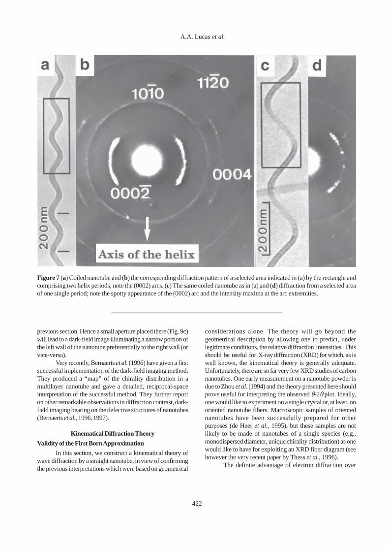
(Bernaerts et al., 1995a), such as the one shown in Figure 6,reveals that the coiled nanotube is actually sharply bent at asuccession of knees joining two straight cylindrical segments.Apart from their short length, the latter have the same structureas the micron-long straight nanotubes of the previous section.The polygonized texture of the coiled nanotube is confirmedby the corresponding diffraction patterns. Selected area EDmicrographs of two helix periods and one single period areshown in Figures 7b and 7d, respectively, alongside bright-field images of the nanotubes (Bernaerts et al., 1995a). Thediffraction spots of each straight segment lie on quasi-continuous circles which are reminiscent of a powder patternof ordinary graphite. But the most conspicuous feature is thefirst order diffraction arc labeled (0002) in Figure 7b. This arc isproduced by the (0002) spots of the successive straightnanotube segments. It reflects the changing orientation of
Figure 4. Sequence of electron diffraction patterns of a nanotube (18 layers with an innermost diameter of about 1.3 nm) obtainedby tilting the vertical nanotube by the indicated angle about a horizontal axis. Note the changes in the spot contrast and in thestreaking intensities. The second order symmetric pairs of spots marked A, B and C, D move toward the twelve o’clock positionupon tilting. The spots C, D belong to achiral, parallel tubules and merge in Fig.4f when the tilt angle is 30°.

420
A.A. Lucas et al.
the segments of which the axis describes a cone around thehelix axis. The angular opening of the arc is related to the helixradius-to-pitch ratio. Note in Figure 7d that the arc is spotty asa result of the “space quantization” of the segment orientationin the polygonized helix. Moreover, the arc is most intense atits edges, which again stems from the extremum nature of thesegment orientation at the edges of the cone it describes.Counting the number of spots in the (0002) arc of Figure 7d orestimating the bend angle in Figure 6 indicates that there mustbe about a dozen straight segments per helix turn.
How can one connect two nanotube segments at anangle of about 30° without grossly distorting the honeycomblattice of each of the graphene layers of the tubes? Remarkably,solutions to this problem were discussed theoretically byDunlap (1992) and by Ihara et al. (1993) even before theobservation of the coiled nanotubes. In Dunlap’s construction,the bending of a single graphene tubule can be accomplished,while maintaining the continuity of the honeycomb lattice, byintroducing a single pentagon at the apex and a singleheptagon diametrically opposed at the saddle point of theknee. A ball-and-stick model of the structure is shown in Figure8 (Fonseca et al., 1995). Chiral as well as achiral tubules of
equal or of different diameters can be connected in this waywith just a single pair of 5-7 ring defects. In a multilayer coilednanotube, the 5-7 rings of the knees in each layer are assumedto be aligned in a common direction (Fonseca et al., 1995).Note that one or several atoms around the 5 and/or the 7 ringscan be removed without causing the collapse of the kneewhich is kept rigid by the rest of the continuous honey-comblattice. Hence, vacancies and vacancy clusters may have beeninserted during the growth process in place of the highlystrained, 5-7 topological defects.
The precise value of the knee angle is still a matter ofdiscussions. A recent study by Zhang and Zhang (1995) usingTEM and ED from a coiled nanotube seen along its axis revealsthat there are just 12 straight segments per helix period in theirparticular sample and hence that the bend angle must be lessthan 30°. This appears to be consistent with Dunlap’sestimation of 30° from his construction (Dunlap, 1994).However molecular model building (Fonseca et al., 1995) aswell as theoretical equilibrium structure calculations (Lambinet al., 1995) suggest that the bend angle should be larger thanor close to 36°, at least in the small diameter tubules which areamenable to such simulations. Note that bending at less than36° can be accomplished by a non diametrically opposed 5-7pair (Ihara et al., 1993). High resolution TEM and EDobservations specifically designed to study the knee regioncould lead to the identification of the actual or most frequentlyoccurring modes of bending in coiled nanotubes.
Sequencing the nanotube chirality
We have discussed the effect introduced by thechirality of individual tubules on the diffraction pattern: eachchiral tubule produces a pair of hexagons of streaking spots(in every diffraction order) whose angular separation, whichis twice the chiral angle, can be measured accurately. But acomplete characterization of a given multilayer nanotubewould require the “sequencing” of the nanotube chirality,that is the specification of the chiral angle of each and everysuccessive tubule of the nanotube. This remarkable featappears to be within reach of high resolution electronmicroscopy by at least two different but related methods, oneworking in real space, the other via reciprocal space. Theprinciple of both methods is illustrated in Figure 9.
The first method would involve an examination of thenanotube bright field image at the best resolution attainabletoday which allows one to resolve the graphene repeat distanceof 0.21 nm between zigzag rows of atoms (Zhang et al., 1993a).Consider, in the image of Figure 1a, one of the lattice fringescorresponding to the edge of a particular tubule whose chiralityis to be determined. The method would consist in tilting thenanotube axis away from the normal to the electron beam untilthe zigzag (curved) “rows” at the edge of the chosen tubuleare brought into alignment with the electron beam. A sketch ofthe tilting experiment is given in Figure 9a,b. When correctlyaligned in this way, the quasi-continuous lattice fringe chosen
Figure 5. Coiled nanotubes of various radii and pitches. Theinset indicates (arrows) than the coils are polygonized.

Electron diffraction by carbon nanotubes
421
on the left side of the tubule in Figure 1a (or on the right side,depending on the chiral handedness) should break up intoresolvable beads separated by 0.21 nm (Fig. 9b). The tilt angleand its sign would then give the chiral angle and handednessof that particular tubule. The method was already used inTEM of biological structures such as the helical arrangementof proteins in the tobacco mosaic virus (Finch, 1972, andreferences therein) and is also reminiscent of a computerexperiment in which a space-filling model of a DNA moleculeis tilted in order to obtain a better view through the small andlarge grooves of the double helix (Rich, 1992). A computersimulation (Bernaerts et al., 1996) has demonstrated thefeasibility in principle of this method. However, several practicalproblems, the most serious of which is the severe radiationdamage caused by the high intensity electron beam in high-resolution TEM, have so far prevented the actualimplementation of this direct approach.
The second method makes use of the diffractioncontrast, dark-field imaging technique. It consists in producingan image of the nanotube by selecting, with a small objectiveaperture, those electrons which have been scattered into a
particular diffraction spot belonging to one hexagonal set ofchosen chiral angle. Such electrons will image primarily thosetubules which are responsible for their diffraction into theselected spot and hence will allow, in principle, a “reading” ofthe position (relative to the bright field image of the nano-tube)of the tubule(s) having the chosen chirality. Among the spotsbelonging to a chiral tubule, the most suitable ones for dark-field imaging are those closest to the twelve o’clock (and sixo’clock) site in the first order diffraction circle (Fig. 9c). Aswas discussed before, a tilting of the tubule axis away fromthe normal to the electron beam will cause these spots toclimb towards the top (and bottom) of the diffraction circleand merge when the tilt angle coincides with the chiral angleof the tubule(s) under scrutiny. This is immediately clear byreferring to Figure 9b again: for the correct chiral alignment,the zigzag atomic helices (drawn as continuous lines in Fig. 9)project into cycloids which have sharp horizontal cusps onthe left (or right) side of the tilted tubule. The regular cuspsgenerate a linear grating in the direction of the tubule axiswhich diffracts the electron waves and give rise to the twomerging streaked spots at twelve o’clock, as discussed in the
Figure 6. High resolution image of a coiled nanotube revealing its polygonized texture. The maximum projection of the polygonangle is about 30°. The inset shows the approximately circular cross section of the nanotube.
422
A.A. Lucas et al.
previous section. Hence a small aperture placed there (Fig. 9c)will lead to a dark-field image illuminating a narrow portion ofthe left wall of the nanotube preferentially to the right wall (orvice-versa).
Very recently, Bernaerts et al. (1996) have given a firstsuccessful implementation of the dark-field imaging method.They produced a “map” of the chirality distribution in amultilayer nanotube and gave a detailed, reciprocal-spaceinterpretation of the successful method. They further reporton other remarkable observations in diffraction contrast, dark-field imaging bearing on the defective structures of nanotubes(Bernaerts et al., 1996, 1997).
Kinematical Diffraction Theory
Validity of the First Born Approximation
In this section, we construct a kinematical theory ofwave diffraction by a straight nanotube, in view of confirmingthe previous interpretations which were based on geometrical
considerations alone. The theory will go beyond thegeometrical description by allowing one to predict, underlegitimate conditions, the relative diffraction intensities. Thisshould be useful for X-ray diffraction (XRD) for which, as iswell known, the kinematical theory is generally adequate.Unfortunately, there are so far very few XRD studies of carbonnanotubes. One early measurement on a nanotube powder isdue to Zhou et al. (1994) and the theory presented here shouldprove useful for interpreting the observed θ-2θ plot. Ideally,one would like to experiment on a single crystal or, at least, onoriented nanotube fibers. Macroscopic samples of orientednanotubes have been successfully prepared for otherpurposes (de Heer et al., 1995), but these samples are notlikely to be made of nanotubes of a single species (e.g.,monodispersed diameter, unique chirality distribution) as onewould like to have for exploiting an XRD fiber diagram (seehowever the very recent paper by Thess et al., 1996).
The definite advantage of electron diffraction over
Figure 7 (a) Coiled nanotube and (b) the corresponding diffraction pattern of a selected area indicated in (a) by the rectangle andcomprising two helix periods; note the (0002) arcs. (c) The same coiled nanotube as in (a) and (d) diffraction from a selected areaof one single period; note the spotty appearance of the (0002) arc and the intensity maxima at the arc extremities.

Electron diffraction by carbon nanotubes
423
XRD is that the scattering power of atoms for electrons issuch that the beam can be focused onto one single nanotubefor diffraction and imaging, as illustrated in the previoussection. This very advantage however usually entails oneinterpretational drawback, namely that the conditions for thevalidity of the first Born or kinematical approximation todescribe the electron scattering quantitatively may be difficultto meet (Gevers, 1970): for heavy materials, the applicability ofthe kinematical theory to the calculation of Bragg spotintensities demands that the thickness of the diffracting objecttraversed by the electron beam be less that 10 nm. For carbonnanotubes however, the conditions should not be so severeon account of the smaller scattering power of the light carbonatom, as we now show.
The kinematic atomic scattering amplitudes fe(q) of
elements for fast electrons have been compiled by Smith andBurge (1962) and by Doyle and Turner (1968) who analyzed
Figure 8. Ball-and-stick model of a single nanotube knee ofabout 30°. The bend is obtained by inserting a pair ofpentagonal and heptagonal ring defects diametrically opposedat the outer elliptic and inner hyperbolic (saddle) points of theknee. The stick connects the aligned 5-7 rings in the twotubules which are separated by the 0.34 nm graphitic distance.
Figure 9. Principle of the tilting experiment to determine thehandedness of a chiral tubule. In (a) a familly of three zig-zagrows of atoms are represented as parallel, right handed spiralsmaking an angle a with the horizontal, tilting axis. In (b) thetubule axis has been tilted by an angle α, its upper tip towardthe viewer; note that the sinusoidal projections of the spiralsin (a) have changed to cycloids in (b) with their sharp cuspsappearing on the left side of the tubule. In (c) the streakedspots at one and eleven o’clock move upon tilting toward thetwelve o’clock position marked A where an aperture is placedfor dark-field imaging of the tubule.

424
A.A. Lucas et al.
scattering factors calculated from realistic atomicwavefunctions. The first Born approximation to high-energyelectron scattering (by the screened nuclear Coulombpotential) used in these calculations is dominant providedthat the “fine structure constant” Ze2/ v = (Zc/v)/137, whereZ is the nuclear charge and v is the electron velocity, is muchsmaller than one (Landau and Lifshitz, 1967). For Z = 6 and for300 keV electrons, a typical electron energy used in the TEM-ED works discussed in the present paper, one finds Ze2/ v ≈0.07, a value indeed small enough to validate the first Bornapproximation. From the tabulated data (Doyle and Turner,1968), one can then estimate a total elastic cross section(including the correction of relativistic length contraction) ofσ Å 2.2 10-2 Å2 per carbon atom. Ignoring coherent scatteringwithin and between the graphene layers, of which the areadensity is about 0.4 atom/Å2, we find that the total scatteringprobability is of order 10-2 per atomic layer. After travelingthrough N layers, the relative Poisson probabilities for singleand double scattering would be 10-2N and 10-4N2/2!respectively. If we demand that the double scattering be lessthan 10 % of the single scattering, N may not exceed 20 layers.
In a quantitative evaluation of the intensity of electronwave diffraction by a crystalline, cartesian material, one
eventually considers the “extinction distances” ξg for Braggbeams characterized by the reciprocal lattice vectors g. In theso-called one-beam kinematical theory (Gevers, 1970), ξg isthe distance traveled after which the wave intensity is totallytransferred by elastic scattering from the forward beam to thediffracted beam g in the exact Bragg orientation. For thekinematical theory to be valid, the thickness traversed by thebeam should be much smaller than all ξg. For electrons ofkinetic energy E and wavelength λ, ξg at the exact Bragg angleis given by ξg Å λE/Vg where Vg is the corresponding Fouriercomponent of the atomic lattice potential for the high-energyelectrons. Vg is related to the atomic scattering amplitude f
e(g)
by
( ) ( )gfm
eVg eaig
2
1 2. h
∑µµ
Ω=
where the Σµ extends over the independent atomic sites aµ inthe graphite unit cell of volume Ω Å 17 Å3. Using again thetable of f
e(g) in Doyle and Turner (1968), one finds Vg Å 0.25
eV for the lowest-order g parallel to the graphene plane. Dueto such a relatively small value of the carbon crystal potential,for E = 300 keV one finds ξg Å 2.5 µm or about 7000 graphitelayers. Hence, in bulk graphite, the forward beam in an exactBragg direction will not be appreciably depleted by elasticscattering until traversing several hundred layers. Fordirections away from an exact Bragg angle, the depletion byeach of the diffracted beams is much reduced (Gevers, 1970).In nanotubes, the turbostratic disorder of successive tubuleswill tend to suppress the coherent Bragg scattering andprevents the build up of amplitude in particular reflections.
We thus reach the conclusion that the kinematicaltheory should be a valid approximation for carbon nanotubesmade of several tens of monolayers and hence the theoryappears to be quite suitable for the nanotubes actuallyobserved in the works reported above.CCV Theory
In formulating our theory, we take the view that astraight monolayer tubule can be constructed by assemblinga finite set of parallel monoatomic carbon helices sharing thenanotube axis. A glance at Figure 2 shows that this can bedone in a number of ways both for achiral and for chiraltubules. We use this approach because there already existsan analytical treatment of diffraction by a regular, monoatomic,circular helix. The theory was developed by Cochran, Crickand Vand in 1952 (Cochran et al., 1952, referred to here as theCCV theory) for the diffraction of X-rays by polypeptide α-helices and was applied to DNA molecules shortly thereafter(Watson and Crick, 1953; Franklin and Gosling, 1953. See alsoKlug et al., 1958; Vainshtein, 1966). These biological moleculesoften can be viewed as collections of C, H, N, O, P, S etc.coaxial helices. The CCV theory turns out to be particularly
Figure 10. Cylindrical coordinates of atoms on a regular circularhelix of pitch P and atomic repeat distance p along the helixaxis.
Electron diffraction by carbon nanotubes
425
straight-forward to apply to straight, circular carbon nanotubessince they have a single type of atoms regularly arrangedalong exactly circular and equidistant coaxial helices. Thetheoretical approach developed here is similar to the oneintroduced earlier by Qin (1994) and was formulated quiteindependently (Lucas et al., 1996).
To set the notations, we provide a particularlystraightforward derivation of the CCV result. The scatteringamplitude of a collection of atoms at fixed positions r
j, is given
by
( ) ( ) ( ) ( )∑≡=j
rik jekfkAkfkT.
where k is the wavevector transfer and f(k) is the kinematicatomic scattering factor for X-rays or for electrons, assumedto be isotropic (the theory can be generalized to “anisotropic”atoms). The diffraction factor A(k) is the Fourier transform ofthe nuclei density
( ) ( )∑ −δ=j jRrrp
On a regular, circular, monoatomic helix of radius r,pitch P and atomic repeat distance p in the z-direction of thehelix axis, the atomic positions are given, in cylindricalcoordinates, by (see Fig. 10)
+=π=φ= ojjjj zjpzzP
rr ,2
,
where j is an integer and (r, φo, z
o) are the coordinates of an
atom taken as a conventional origin. To evaluate equation (1)in cylindrical coordinates according to equation (2), we usethe Jacobi-Anger expansion of a plane wave in Besselfunctions (Arfken, 1985):
+=π=φ= ojjjj zjpzzP
rr ,2
,
where
=ψ+⊥= −
x
ykyx k
kkkk 122 tan,
and k = (kx,k
y,k
z) are the cartesian coordinates of the
wavevector transfer. This relation can be readily demonstratedby noting that the plane wave, being a periodic function of ϕ,can be expanded in the Fourier series (eqn. 3) of exp(-inϕ); the
expansion coefficients are obtained, in the usual way, as anintegral of the left hand side of equation (3) multiplied byexp(inϕ), which yields the Bessel function J
n and the other
phase factors in equation (3). Substituting equations (3) and(2) into equation (1), the summation over j in (1) can then beperformed by using the well known identity
∑∑
+ππ−δ=
π−
mz
j
jp
pnpki
p
m
Pke
z
22
The result is the CCV formula:
( ) ( )
( ) ozok zikin
n
in
mnz
erkJe
p
m
P
nkkfkT
+φ−
π+ψ⊥
×
+π−δ= ∑
2
,
2
The diffracted intensity is the square modulus of thisexpression. The δ-function means that the intensity is nonzeroonly on horizontal “layer-lines” [Polanyi (1921): the basicconcept of layer-planes and layer-lines in the X-ray structuresof fibers is implicit in this paper. The word “layer-line”(Schichtlinie) first appears in this paper and has been usedever since to describe X-Ray fiber diagrams). The layer-linesare positioned at
Tp
m+
P
n=k z
122 π≡
π
If P/p is irrational, kz can take all real values. If P/p is
rational the layer-lines occur only at discrete values of kz =
2πl/T where l is an integer and T, the true helix period, is thesmallest common multiple of P and p.
We can now apply this result to a nanotube.As Figure 2 illustrates, a tubule of arbitrary chirality
can conveniently be specified by two integers (L,M) givingthe position of the hexagonal atomic cell which, on rolling upa flat sheet of graphene to make a seamless tubule, is broughtin coincidence with the cell at the origin (Hamada et al., 1992).Parallel and perpendicular achiral tubules are of the type (L,0)and (M,M), respectively. Let us arbitrarilly choose in Figure2a one of the zig-zag rows of atoms which makes a nonzeroangle with respect to the tubule circumference C. In Figures2b, c or d, these atoms make two helices related to one anotherby a single screw operation (z
1, ϕ
1). Shifting this zig-zag pair of
helices L 1 times by the tubule helical symmetry operation (zo,
ϕo) covers the tubule completely (discussions of helical
(1)
(2)
(3)
(4)
(6)
(5)

426
A.A. Lucas et al.
symmetries of nano-tubes have been given by Klein et al.,1993, White et al., 1993, and Dresselhaus et al., 1995). Thediffraction amplitude of the complete tubule is thereforeobtained by adding up the amplitudes, as given by equation(5), of a finite set of L helix pairs. Since the successiveamplitudes differ only by phase factors, the total amplitudewill involve summing a geometrical series.
Diffraction by an Achiral Tubule
As an illustration of how the method worksmathematically, let us consider the simple case of a paralleltubule (L,0) (Fig. 2c). From equation (1), an initial zig-zag pairof helices separated by the pure translation (z
1=d,ϕ
1=0) along
the z-axis will produce the scattering amplitude
( ) ( )( )11. zik
j
Rikpair
zj eekA += ∑
where z1 = d Å 0.14 nm is the C-C bond distance. Note in
passing that the pair amplitude vanishes if kzz
1 is an odd
multiple of π. This happened to be the case for the celebratedB-DNA molecule (Franklin and Gosling, 1953) which has twohelical strands displaced by z
1 = 3P/8 and of which the X-ray
fiber diagram indeed shows a missing 4th layer-line (kzz
1 = 3π).
If we now subject the pair of helices to L-1 puretranslations (z
o=3d, ϕ
o=0) along the z-axis and add up the
amplitudes (7) for each pair, the amplitude gets multiplied bythe geometrical series
∑−
=
1
0
L
n
zink oze
The result is
( ) ( )oz
ozzj
ziK
ziLKzk
j
ik.Rtub
e
eee(=kA
−−+∑
1
11 11
The first factor is the amplitude of a single helix, asgiven in equation (5); the second means that there are twokinds of inequivalent helices in the tubule, just as there aretwo inequivalent atoms in the hexagonal unit cell of thehoneycomb lattice; and the last factor gives the interferencebetween all the pairs in the complete tubule. Because in aparallel tubule the helix period is P = Lz
o = 3dL and because k
z
is quantized to the layer-lines kz = 2πl/P, this last factor amounts
to
sLlLli
li
ziK
ziLk
Le
e=
e
eoz
oz
,/2
2
1
1
1
1 δ=−−
−−
π
π
where the Kronecker δl,sL
suppresses all layer-lines exceptthose at l = sL, s integer. The diffraction pattern is thereforeconfined to layer-lines separated by integer multiples of 2πL/P = 2π/3d which is the expected result since, in the paralleltubule, the repeat distance in the z-direction is 3d. Along eachallowed layer-line, the intensity is given by a linear combinationof Bessel functions. As will be seen in the computersimulations, the overall result is a mm2-symmetric hexagonalset of spots streaking, in an oscillatory fashion, away from thetubule axis.
Diffraction by a Chiral Tubule
We now formulate the result of the application of theCCV theory to the diffraction amplitude of a general chiraltubule specified by the two arbitrary integers (L,M). Thepattern is again organized in layer-lines labeled by an integerl. The total scattered amplitude along the l’th layer-linefactorizes as follows:
( ) ( ) ( ) ( )2/π+ψ∑ ⊥ kin
n ntub erkJkf=kT
An (L,M) B
n (L,M)
The scattered intensity is the square modulus of thisexpression. The factors have the following meaning: f(k), J
n
and ιk have been defined before in equations (1) and (3);
An(L,M), represents the contribution of the two inequivalent
helices of the tubule, as in equation (8), and is given by
( ) ( )Tlznin
lle=ML,A /21 π+φ−+
Bn(L,M) is the factor associated with the summation over L
pairs of helices making up the complete tubule:
( ) ( )[ ]( )[ ]/Tzl2+ni
L/Tzl2+ni=MLB
oo
oon πφ−−
πφ−−exp1
exp1,
Let us denote by C the circumference of the tubule in units ofthe honeycomb lattice parameter d√3. This is given by
( )222MLML=
3d
r=C ++π
The sum over n in equation (10) is restricted to integer values
(7)
(8)
(9)
(10)
(11)
(12)
(13)

Electron diffraction by carbon nanotubes
427
of n satisfying the selection rule of the l’th layer-line
l = nq + mp
where m is an integer and p, q are integers obtained afterreduction of the rational fraction
2M+L
C=
q
p 22
Irrespective of the chirality, the true helix period T is always aninteger multiple of the atomic period along the axis of a carbonhelix and is given by (Dresselhaus et al., 1995):
dC
Lp=T
2
3
Finally the screw operations (ϕο,zo) and (ϕ
1,z
1) are obtained
from
,C
M+L=o πφ
2
2
dC
M-=zo
2
3
These formulae are arrived at by simple geometricalconstructions in the plane of the honeycomb lattice.
Then, taking equations (14)-(18) into account, somealgebra shows that the factor in equation (12) simply reducesto
Bn = L Σ
sδ
n+mM,sL
where s in any integer. The effect of the Kronecker δ-functionsis to eliminate all layer-lines pertaining to the single, originalhelix pair and to leave only such layer-lines as will constructtwo hexagonal patterns of spots each rotated by the chiralangle ± α with respect to the mm2-symmetric position (i.e., theposition characteristic of an achiral (L,0) tubule). Due to theoscillations of the Bessel functions, each “spot” is a streakfading away in an oscillatory fashion perpendicular to themeridional axis of the pattern.
Computer Simulations
We now illustrate the theory with computer simulationsof the diffraction by straight tubules and nano-tubes. In thecalculations, we have used the actual kinematic form factorfor carbon such as listed by Doyle and Turner (1968). Since in
electron microscopy work, the spot intensities are seldommeasured quantitatively, our simulations will at this stage serveonly to confirm the capability of the theory to obtain thequalitative features of the diffraction patterns.
We note that the complete formula in equations (10)-(12) is computationally extremely efficient: the only variableinput is the pair of integers (L,M) which give the tubule sizeand chirality. The position of each layer-line of nonvanishingintensity is determined in advance by the purely geometricalfactor B
n(L,M); and along a given layer-line, the intensity
calculation demands only a few dominant Bessel functions.Due to the closed form of the formula, the computing time isindependent of tubule size. By contrast, the brute forcecalculation of the scattering from the thousands of individualatoms would require constructing their coordinates andsweeping the reciprocal space in search of the diffractionspots.Monolayer tubules: normal incidence
In the spirit of our approach of building up a tubule byassembling a set of helices, we first present the result of acomputer experiment: Figure 11 shows the successive patternsobtained by diffraction, at normal incidence, from an increasingnumber of helix pairs, beginning with just one pair (Figure11a) and ending with the full complement of L=18 pairs of acomplete (18,0) parallel tubule (Fig. 11d). In Figure 11a, onerecognizes the diamond and maltese cross structurescharacteristic of the diffraction by a regular helical moleculesuch as the celebrated DNA (Franklin and Gossling, 1953).There are many layer-lines along which the intensity is givenby a dominant Bessel function of increasing order. Note thatthe regions about the long diagonals of the diamonds areextinguished by the destructive interference between thewaves scattered by the two inequivalent helices (in thissimulation, the two inequivalent helices were chosen to beconnected by parallel C-C bonds shown in the perspectivedrawing below the pattern; note that this choice of startinghelix pair, which corresponds to the analytical formulae ofequation 18, is different from the zig-zag pair discussedpreviously. The end result of the simulation for the completetubule is of course independent of this choice). In the nextthree patterns produced by 6, 12 and 18 helix pairs, the layer-lines are seen to become progressively removed by destructiveinterferences, except for those destined to build up the finalhexagonal, mm2 symmetry pattern.
The spots are elongated perpendicular to the tubuleaxis: this is the streaking phenomenon observed in the real EDpatterns (Iijima, 1991; Iijima and Ichihashi, 1993; Zhang et al.,1993b). The intensity modulation of the zeroth layer-line isessentially a representation of the oscillations of the zerothorder Bessel function. This central line would be the only onepresent if the scattering pattern was produced by a smooth,continuous cylinder of the same radius. The oscillationsbasically represent a slit function and arise from the interference
(14)
(15)
(16)
(17)
(18)
(19)

428
A.A. Lucas et al.
Figure 11. Computer simulations of the diffraction patterns of an increasing number of helix pairs from one pair (a) to the completeset of 18 pairs (d) making up the complete (18,0) tubule. The diamond repeat of the maltese cross characteristic of atomic helicesin (a) is seen to evolve into the hexagonal spot pattern of a tubule in (d) by the destructive interference removal of intervening layerlines in (b) and (d).

Electron diffraction by carbon nanotubes
429
between waves scattered by the two edges of the cylinder.Such a continuous tube has only one characteristic length, itsdiameter, which sets the length scale for the argument of theBessel function. This is further demonstrated by Figure 12which is the normal incidence diffraction pattern of a (36,0)parallel tubule. The oscillation frequency in the zeroth layer-line has doubled in comparison with Figure 11d. The streakingspots now also exhibit intensity oscillations which reflect thesame interference effect of the tubule edges. These streakmodulations were barely visible in the less contrasted pictureof the smaller (18,0) tubule. The enhanced contrast in the(36,0) pattern also reveals the second order hexagon ofstreaking spots. The present interpretation of the modulatedstreak intensities was already provided by Iijima and Ichihashi(1993) in terms of Fraunhofer diffraction from the two portionsof the tubule parallel to the incident electron beam.
Figure 13 shows the simulated diffraction of an (18,1)chiral tubule. There are now two first order hexagonal sets ofspots which are obtained from the achiral parallel hexagon ofFigure 10d by clockwise and counterclockwise rotations bythe small chiral angle cos-1[(2L+M)/2C] Å 2.68°. Note that thetwelve o’clock streak has split into two symmetric modulatedstreaks, leaving zero intensity on the (projection of the) tubuleaxis.
Although only the amplitudes are additive and notthe intensities, one expects that the general geometrical
features in the diffraction pattern of a multilayer nanotube willreflect the patterns of individual tubules such as shown inFigures 12 and 13. Since the chiral angle can vary from zero(parallel tubule) to 30° (perpendicular tubule), a nanotube willusually contain a number of tubules with small chiral angles,say of the order of or smaller than 10°. Such tubules willproduce overlapping horizontal streaking spots near the twelveo’clock (and six o’clock) positions, because the streaking isnearly tangent to the first order circle around these positions.Due to the finite resolution in the ED micrograph, this overlapwill therefore result in thick and long streaks about one and 11o’clock. The other four hexagonal spots of each tubulehowever will give rise to well resolved pairs of nonoverlappingstreaks, as in Figure 13. This explains the frequently observedreinforced streaks at the top and bottom of the first orderdiffraction circle, such as those shown in Figures 1b and 4.For a nanotube containing a majority of nearly perpendiculartubules, the horizontal streak reinforcement should appear attwelve o’clock in the second-order circle, as in Figure 3b.Monolayer tubules: oblique incidence
We have performed calculations of the diffraction ofan electron beam by a tubule at various incidence angles, inorder to simulate a tilting experiment such as the one shown inFigure 4. A large (25,10) tubule of 2.41 nm diameter and 16°chiral angle was selected for the simulation. The fourdiffraction patterns in Figure 14 correspond to tilting the tubule
Figure 12. Computer simulation of the diffraction pattern of a(36,0) tubule. The modulation frequency of the streaks isdoubled as compared to the case of the twice smaller (18,0)tubule in Figure 11d.
Figure 13. Computer simulation of the diffraction pattern ofan (18,1), nearly parallel, chiral tubule. There are now two setsof hexagonal streaked spots turned with respect to each otherby twice the chiral angle of 2.68°.

430
A.A. Lucas et al.
axis away from the beam normal by an angle θ of 0, 10, 20 and30 degrees, respectively. The detailed effect of tilting thesample can be computed from Eqn. (10) by rotating the transferwavevector k by an angle θ around the y-axis in the oppositedirection.
One observes that the layer-lines recede from thezeroth order layer-line when θ increases. Measuring distancesbetween layer-lines in the direction of the tubule axisconfirms that they increase like 1/cosθ. This “chirping” inreciprocal space corresponds to a decrease of the apparentaxial lattice spacing, as seen by the electron waves, by a factorcosθ (this is easily verified by considering a simple line gratingat oblique incidence, see Amelinckx et al., 1995a). The otherstriking effect of the tilting on the diffraction pattern is the“climbing motion” of the pair of spots marked A,B and C,D
towards the twelve o’clock position on their respective circles.They form a single streak when θ = 20° and beyond but thesimulation shows that they began to coalesce when θ nearedthe chiral angle of 16°. This behavior reproduces qualitativelythe observation of Figure 4. It justifies setting the dark-fieldimaging aperture at twelve o’clock to measure the chiral angleof a tubule or set of tubules, as discussed previously (Fig. 9c).
Multilayer Nanotubes
A nanotube containing N coaxial tubules separatedby the graphite interlayer spacing c
o Å 0.34 nm is fully specified
by giving i) a set of integer pairs (Lm,M
m), m = 1,...,N, specifying
the chirality sequence and ii) the relative registry between thesuccessive tubules, i.e. the cylindrical coordinates (r
m,ϕ
om,z
om)
Figure 14. Computer simulation of the diffraction patterns obtained by tilting the axis of a (25,10) tubule through the indicatedangles. This computer experiment simulates qualitatively the real experiment shown on Figure 4. Note the motion of the spots A,B and C, D upon tilting.

Electron diffraction by carbon nanotubes
431
of a set of initial atoms in the tubules. The (Lm,M
m) pairs
should satisfy, up to a small tolerance of at most a few percent, the condition that the circumference C
m given by
equation (13) increases by 2πco/ Å 8.81 from one tubule to the
next in the set. Starting from an inner tubule of radius C1, a
possible tubule set can be read off the honeycomb lattice of
Figure 15 in which successive concentric equidistant circlesof radii C
m have been drawn. Any pair (L,M) representative of
a lattice point sitting on or near (to within the tolerance) one ofthe circles, defines an acceptable tubule of the set. Figure 15makes it clear that for fixed external dimensions C
1 and C
N of
the nanotube, there can be several sets of tubules differing bytheir chirality (and handedness) and that the bigger thenanotube size, the larger this chirality degeneracy. The highlyefficient diffraction formula for a complete tubule developedin this paper allows the simulation of the diffraction patternscorresponding to all possible chirality sequences compatiblewith the above construction rules. The observed TEM/EDchirality map discussed before (Bernaerts et al., 1996).
When two or more coaxial tubules are considered,interferences are expected from adding the complex diffractionamplitudes of individual tubules. Three sets of parametersare expected to govern interference effects: (i) the newcharacteristic distance c
o Å 0.34 nm will produce periodic
reinforcements of diffracted intensities in the direction normalto the nanotube axis; (ii) different chirality sequences will leadnot only to different spot patterns but also to different,nonadditive spot intensities; (iii) changing the relative tubuleregistry by gliding or rotating the tubules with respect to eachother about their common axis should also affect the spotintensities. In this paper, we will explore only the first twoeffects.
We can easily predict the major interference effectassociated with the interlayer distance c
o. Indeed we expect a
constructive interference when k⊥ Å 2πn/co along the zeroth
order layer-line where n is a nonzero integer. If all the tubuleradii r
m are much larger than c
o, the arguments of the Bessel
functions in equation (10) will be large as soon as we leave thecenter of the diffraction pattern towards the first order circle:k⊥ r
m Å 2πnr
m/ c
o = C
mn/ c
o Å 13n for, say, an (18,0) tubule. We
can then make use of the approximate expression of thedominant Bessel function J
o(x) for large argument x = k⊥ r
(Abramowitch and Stegun, 1984): Jo(x) Å cos(x-π/4). Adding
the various terms for tubule radii rm = r
1 + m c
o, we see that the
phase in the cosine changes by 2π from one tubule to thenext. Ignoring the slow decrease of the J
o oscillation
ampli-tudes, the end result is a total amplitude at k⊥ = 2πn/co
growing like the number N of tubules and the intensity of the(0002n) spot growing like N2. This quantitatively explains theappearance of the (0002n) sets of spots as the principal featurein the diffraction pattern of every multilayer nanotube. Figure16 confirms this behavior. It shows the intensity of the zerothlayer-line in the calculated diffraction pattern of Figure 1c.The nanotube comprises 7 tubules whose radii and chiralities(see the figure caption) have been chosen to simulate Figure1a and the observed chiral angles of the diffraction pattern inFig. 1b. The zeroth layer-line (Figs. 1c and 16) exhibits thepredicted strong reinforcements corres-ponding to theobserved (0002n) spots and, in addition, shows intervening
Figure 15. Construction in the graphene lattice of tubulecircumferences for coaxial tubules separated by the graphiticdistance of 0.34 nm. All lattice points sitting on or near thecircles define possible tubules for a multilayer nanotube.
Figure 16. Simulated intensity distribution along the zerothlayer-line produced by the 7-layers nanotube of Figure 1cshould be helpful in guiding and narrowing down theexploration of the “chirality space” of a nanotube.
432
A.A. Lucas et al.
oscillations due to the interference of the two nanotube walls(the Young two-slits experiment). The agreement betweensimulated and observed patterns is not completely satisfactorybut could certainly be improved by searching the chiralityand registry space of the 7-layers nanotube, as explainedbefore.
Discussion
This paper has presented a short review of TEM-EDobservations of straight and coiled nanotubes. In thedescription of the observed patterns, the emphasis was puton the important characteristics which call for a quantitativetheory of electron diffraction by nanotubes. Such a completetheory was developed for the straight nanotubes comprisingany number of tubules of arbitrary chiralities and the simulatedpatterns based on this theory were successfully comparedwith the observed ones.
We wish to close this paper by pointing out a numberof opportunities offered by the new theoretical approach.
The computer-efficient theory allows for the simulationof the diffraction by nanotubes with defects. For exampleatomic vacancies or vacancy clusters can be easily simulatedby subtracting the amplitudes of the missing atoms from theperfect nanotube amplitude. Another example is the case ofan “excentric” nanotube, i.e., having one or several missinglayers which eventually produce anomalous lattice fringespacings in the TEM image of the nanotube (Bernaerts et al.,1996). This situation simply requires adding the amplitudes ofnon coaxial but parallel tubules.
Very recently, Thess et al. (1996) have succeeded inproducing, by carbon laser ablation, “ropes” ofmonodispersed, parallel (10,10) perpendicular tubules and havetaken a powder XRD diagram of the material. The presenttheory is ideally suited to compute the fiber and powderdiagram of such a system since it provides the exact tubulemolecular form factor from which to calculate the diffractionof the ordered triangular lattice of tubules in the “rope”.
Other helical structures of light elements such as thecarbon conical scrolls (Amelinckx et al., 1992) and the BN andBCN nanotubes recently discovered (Tenne, 1995; Stephanet al., 1994) are ameanable to an application of the presenttheory since they can be described as an ensemble of regularhelices. The theory will also be found useful for interpretingX-ray diffraction data from nanotubes made of heavy elementssuch as the disulfide MoS
2, WS
2 (e.g., Tenne, 1995).
Certain fundamental extensions of the theory arerequired to deal with coiled nanotubes. Since these are madeup from connected pieces of straight cylindrical segments, itwill be necessary to account for the finite length of the straightsections and of the irregular atomic arrangement in theconnecting knee regions which contain ring defects (Ivanovet al., 1994). The latter must be introduced numerically, atom
by atom, while the former can be handled analytically viaequations (4) and (5) in which the δ-function is replaced by aslit-function giving the diffraction amplitude of a helix of finitelength.
Nanotubes containing cylindrical scrolls (Amelinckxet al., 1995b) pose a special simulation problem. They requirethe diffraction amplitude of helices of finite length woundaround a circular cone. This can be written analytically andinvolves derivatives of the cylindrical Bessel functions(Abramowitz and Stegun, 1984). Work along these lines is inprogress.
Acknowledgements
We thank Dr. S. Iijima for allowing the reproduction ofFigures 1a,b and Dr. Qin for informing us about his work (Qin,1994). We are grateful for the support of the following agencies:the Belgian National Science Foundation, the Ministry ofSciences, the European Commission HCM program, theWalloon Government.
References
Abramowitz M, Stegun IA (1984) Pocketbook ofMathematical Functions. Verlag Harri Deutsch, Frankfurt, p.108.
Amelinckx S, Luyten W, Krekels T, Van Tendeloo G,Van Landuyt J (1992) Conical helically wound, graphitewhiskers: a limiting member of the “fullerenes?”. J. Cryst.Growth 121, 543-558.
Amelinckx S, Zhang XB, Bernaerts D, Zhang XF,Ivanov V. B’Nagy J (1994) A formation mechanism forcatalytically grown shaped graphite nanotubes. Science 265,635-639.
Amelinckx S, Bernaerts D, Van Tendeloo G, VanLanduyt J, Lucas AA, Mathot M, Lambin Ph (1995a) Themorphology, structure and texture of carbon nanotubes: anelectron microscopy study. In: Physics and Chemistry ofFullerenes and Derivatives. Kuzmany H, Fink J, Mehring M,Roth S (eds.). World Scientific, Singapore, pp. 515-541.
Amelinckx S, Bernaerts D, Zhang X.B, Van TendelooG, Van Landuyt J (1995b) A structure model and growthmechanism for multishell carbon nanotubes. Science 267, 1334-1338.
Arfken G (1985) Mathematical Methods for Physicists,Academic Press, N.Y., p. 585.
Bacsa WS, De Heer WA (1995) Optical properties ofaligned carbon nanotubes. In: Physics and Chemistry ofFullerenes and Derivatives. Kuzmany H, Fink J, Mehring M,Roth S (eds.). World Scientific, Singapore, pp. 574-577.
Baker RTK (1989) Catalytic growth of carbon filaments.Carbon 27, 315-323.
Bernaerts D, Zhang XB, Zhang XF, Amelinckx S, Van

Electron diffraction by carbon nanotubes
433
Tendeloo G, Van Landuyt J, Yvanov V, B’Nagy J (1995a)Electron microscopy study of coiled carbon nanotubules. Phil.Mag. A71, 605-630.
Bernaerts D, Amelinckx S, Op de Beeck M, VanTendeloo G, Van Landuyt J (1996) The chirality of carbonnanotubules determined by dark field electron microscopy.Phil. Mag. 74, 723-740.
Bernaerts D, Lucas A, Amelinckx S (1997) On a peculiarcontrast effect associated with carbon nano-tubes, Phil. Mag.76, 267-270.
Bethune DS, Kiang CH, de Vries MS, Gorman G, SavoyR, Vazquez J, Beyers R (1993) Cobalt-catalysed growth ofcarbon nanotubes with single-atomic-layer walls. Nature 363,605-607.
Charlier J-C, Michenaud J-P (1993), Energetics ofmultilayered carbon tubules. Phys. Rev. Lett. 70, 1858-1861.
Cochran W, Crick FHC, Vand V (1952) The structure ofsynthetic polypeptides. I. The transform of atoms on a helix.Acta Cryst. 5, 581-586.
Colbert D, Smalley RE (1995) Electric effects in nanotubegrowth. Carbon 33, 921-924.
Colbert DT, Zhang J, McClure SM, Nikolaev P, ChenZ, Hafner JH, Owens DW, Kotula PG, Carter CB, Weaver JH,Rinzler AG and Smalley RE (1994) Growth and sintering offullerene nanotubes. Science 266, 1218-1222.
de Heer WA, Bacsa WS, Châtelain A, Gerfin T,Humphrey-Baker R, Forro L, Ugarte D (1995) Aligned carbonnanotube films: Production, optical and electronic properties.Science 270, 1179-1180.
Doyle PA, Turner PS (1968) Relativistic Hartree-FockX-ray and electron scattering factors. Acta Cryst. A24, 390-397.
Dresselhaus MS, Dresselhaus G, Suguhara K, SpainIL, Goldberg HA (1988) Graphite Fibers and Filaments. SpringerSeries in Materials Science. Vol. 5, Springer-Verlag, Berlin.
Dresselhaus MS, Dresselhaus G, Saito R (1992) Carbonfibers based on C
60 and their symmetry. Phys. Rev. B45, 6234-
6242.Dresselhaus MS, Dresselhaus G, Saito R (1995) Physics
of carbon nanotubes. Carbon 33, 883-891.Dunlap BI (1992) Connecting carbon tubules. Phys.
Rev. 46, 1933-1936.Dunlap BI (1994) Relating carbon tubules. Phys. Rev.
49, 5643-5651.Ebbesen TW (1994) Carbon nanotubes. Annu. Rev.
Mater. Sci. 24, 235-264.Ebbesen TW, Ajayan PM (1992) Large-scale synthesis
of carbon nanotubes. Nature 358, 220-222.Ebbesen TW, Ajayan PM, Hiura H, Tanigaki K (1994)
Purification of nanotubes. Nature 367, 519-519.Finch JT (1972) The hand of the helix of Tobacco
Mosaic Virus. J. Mol. Biol. 66, 291-294.Fonseca A, Hernadi K, B’Nagy J, Lambin Ph, Lucas
AA (1995) Model structure of perfectly graphitizable coiledcarbon nanotubes. Carbon 33, 1759-1775.
Franklin RE, Gosling RG (1953) Molecular configurationin sodium thymonucleate. Nature 171, 740-741.
Gamaly EG, Ebbesen Th (1995) On the mechanism ofcarbon nanotube formation in the arc-discharge. In: Physicsand Chemistry of Fullerenes and Derivatives. Kuzmany H,Fink J, Mehring M, Roth S (eds.). World Scientific, Singapore,p. 546-550.
Gevers R (1970) Kinematical theory of electrondiffraction. In: Modern Diffraction and Imaging Techniquesin Material Science. Amelinckx S, Gevers R, Remaut G, VanLanduyt J (eds.). North Holland, Amsterdam. p. 1.
Guo T, Nikolaev P, Thess A, Colbert DT, Smalley RE(1995a) Catalytic growth of single-walled nanotubes by laservaporization. Chem Phys Lett 243, 49-54.
Guo T, Nikolaev P, Rinzler A, Tomanek D, Colbert D,Smalley RE (1995b) Self-assembly of tubular fullerenes. J. Phys.Chem. 99, 10694-10697.
Hamada N, Sawada S, Oshiyama A (1992) New one-dimensional conductors: graphitic microtubules. Phys. Rev.Lett. 68, 1579-1581.
Henrard L, Senet P, Lambin Ph, Lucas AA (1996) Onthe ultraviolet spectrum of multishell fullerenes and its role aspossible component of interstellar dust. Full. Sci. Technol. 4,131-163.
Hiura H, Ebbesen TW, Tanigaki K, Takahashi H (1993)Raman studies of carbon nanotubes. Chem. Phys. Lett. 202,509-512.
Hsu WK, Hare JP, Terrones M, Kroto HW, WaltonDRM, Harris PJF (1995) Condensed-phase nanotubes. Nature377, 687-689.
Ihara S, Itoh S, Kitakami JI (1993) Helically coiled cageforms of graphitic carbon. Phys. Rev. 48, 5643-5647.
Iijima S (1991) Helical microtubules of graphitic carbon.Nature 354, 56-58.
Iijima S, Ichihashi T (1993) Single-shell carbonnanotubes of 1-nm diameter. Nature 363, 603-605.
Itoh S, Ihara S (1993) Toroidal forms of graphitic carbon.II. Elongated tori. Phys. Rev. 48, 8323-8328.
Ivanov V, B’Nagy J, Lambin Ph, Lucas A, Zhang XB,Zhang XF, Bernaerts D, Van Tendeloo G, Amelinckx S, VanLanduyt J (1994) The study of carbon nanotubules producedby catalytic method. Chem. Phys. Lett. 223, 329-335.
José-Yacaman M, Miki-Yoshida M, Rendon L,Stantiesteban JG (1993) Catalytic growth of carbonmicrotubules with fullerene structure. Appl. Phys. Lett. 62,202-204.
Kawaguchi M, Nozaki K, Motojima S, Iwagana H (1992)A growth mechanism of regularly coiled carbon fibers throughacetylene pyrolysis. J. Cryst. Growth 118, 309-312.
Klein DJ, Seitz WA, Schmaltz TG (1993) Symmetry ofinfinite polymers: application to buckytubes. J. Phys. Chem.
434
A.A. Lucas et al.
97, 1231-1236.Klug A, Crick FHC, Wyckoff HW (1958) Diffraction by
helical structures. Acta Cryst. 11, 199-213.Krätschmer W, Lamb LD, Fostiropoulos K, Huffman
DR (1990) Solid C60: a new form of carbon. Nature 347, 354-358.
Kroto HW, Heath JR, O’Brien SC, Curl RF, Smalley RE(1985) C60: Buckminsterfullerene. Nature 318, 162-163.
Lambin Ph, Fonseca A, Vigneron JP, B’Nagy J, LucasAA (1995) Structural and electronic properties of bent carbonnanotubes, Chem. Phys. Lett. 245, 85-89.
Landau L, Lifchitz E (1967) Mécanique Quantique(Quantum Mechanics). Edition Mir, Moscow, USSR, p. 565.
Langer L, Bayot V, Issi J-P, Stockman L, VanHaesendonck C, Bryunseraede Y, Heremans JP, Olk CH (1995)Electrical Resistivity of Carbon Nanotubes. In: Physics andChemistry of Fullerenes and Derivatives. Kuzmany H, Fink J,Mehring M, Roth S (eds.). World Scientific, Singapore, p. 565-569.
Liu M, Cowley JM (1994a) Structures of the helicalcarbon nanotubes. Carbon 32, 393-403.
Liu M, Cowley JM (1994b) Structures of carbonnanotubes studied by HRTEM and nanodiffraction.Ultramicroscopy 53, 333-342.
Lucas AA, Bruyninckx V, Lambin Ph (1996) Calculatingthe diffraction of electrons or X-rays by carbon nanotubes.Europhys. Lett. 35, 355-360.
Lu JP (1995) Novel magnetic properties of carbonnanotubes. Phys. Rev. Lett. 74, 1123-1126.
Mintmire JW, Dunlap BI, White CW (1992) Arefullerene tubules metallic? Phys. Rev. Lett. 68, 631-634.
Polanyi M (1921) Das Röntgen-Faserdiagramm. (TheX-ray fiber diagram). Z. Phys. 7, 149-180.
Qin LC (1994) Electron diffraction from cylindricalnanotubes, J. Mater. Res. 9, 2450-2456.
Rich A (1992), Molecular recognition between proteinand nucleic acids. In: The Chemical Bond. Zewail A (ed.).Academic Press, Boston, pp. 31-86.
Robertson DH, Brenner DH, Mintmire DW (1992)Energetics of nanoscale graphitic tubules. Phys. Rev. B45,12592-12595.
Rodriguez NM (1993) A review of catalytically growncarbon nanofibers. J. Mater. Res. 8, 3233-3250.
Smith GH, Burge RE (1962) The analyticalrepresentation of atomic scattering amplitudes for electrons.Acta Cryst. 15, 182-186.
Stephan O, Ajayan PM, Colliex C, Redlich Ph, LambertJM, Bernier P, Lefin P (1994) Doping graphitic and carbonnanotube structures with boron and nitrogen. Science 266,1683-1685.
Tenne R (1995) Doped and heteroatom-containingfullerene-like structures and nanotubes. Adv. Mat. 7, 965-972,989-995.
Thess A, Lee R, Nikolaev P, Dai H, Petit P, Robert J, XuCh, Lee YH, Kim SG, Colbert D, Scuseria G, Tomanek D, FischerJ, Smalley R (1996). Crystalline ropes of metallic carbonnanotubes. Science 273, 483-487.
Vainshtein BK (1966) Diffraction of X-Rays by ChainMolecules. Elsevier, Amsterdam. pp. 150-151.
Verwerft M, Luyten W, Amelinckx S. (1990), Tworemarkable defect related electron diffraction effects. Microsc.Microan. Microstruct. 1, 167-173.
Watson J, Crick FHC (1953) A structure of deoxy-ribosenucleic acid. Nature 171, 737-738.
White CT, Robertson DH, Mintmire JW (1993) Helicaland rotational symmetries of nanoscale graphitic tubules.Phys. Rev. B47, 5485-5488.
Zhang XB, Zhang XF, Bernaerts D, Van Tendeloo G,Amelinckx S, Van Landuyt J, Ivanov V, B’Nagy J, Lambin Ph,Lucas A (1994) The texture of catalytically grown coil-shapecarbon nanotubules. Europhys. Lett. 27, 141-146.
Zhang XF, Zhang Z (1995) Polygonal spiral of coil-shaped carbon nanotubules. Phys. Rev. B52, 5313-5317.
Zhang XF, Zhang XB, Van Tendeloo G, Amelinckx S,Op de Beeck M, Van Landuyt J (1993a) Carbon nanotubes;their formation process and observation by electronmicroscopy, J. Cryst. Growth 130, 368-382.
Zhang XF, Zhang XB, Amelinckx S, Van Tendeloo G,Van Landuyt J (1993b) The reciprocal space of carbon-tubes :a detailed interpretation of the electron diffraction effects,Ultramicroscopy 54, 237-249.
Zhou O, Fleming RM, Murphy DW, Chen CH, HaddonRC, Ramirez AP, Glarum SH (1994) Deffects in carbon nano-structures. Science 263, 1744-1747.
Discussion with Reviewers
M.S. Dresselhaus: In reading the paper I wanted to knowhow electron microscopy could distinguish between cylindersand scrolls.Authors: The only, admittedly indirect, TEM evidence forscrolls is the observation (Bernaerts et al., 1995b) of anomalousspacings between basal lattice fringes in one wall or the otherin the bright field image of a nanotube. The interpretation interms of scrolls is consistent with the frequent finding thatthe number of distinct chiral angles is less than the number oftubules in a nanotube, a multiturn scroll having of course aconstant chiral angle. One or several missing tubules in ananotube would also lead to singular fringe spacings(Bernaerts et al., 1997) as a result of the van der Waals attractionof the inner portion of the nanotube towards the outer layers,although this interpretation would not explain the paucity ofchiralities. The issue could be resolved by the chance imagingof a nanotube fragment along its axis.M.S. Dresselhaus: I wonder whether resonances due toperiodic stacking of nanotube arrays could be found. In view

Electron diffraction by carbon nanotubes
435
of the interest in the single wall nanotubes produced by theRice group (Thess et al., 1996), some comments on what TEMcan tell us about these materials would be of interest.Authors: As stated the scattering amplitude of a single tubulewill serve as the molecular form factor for the scattering by atubule array, the total scattering amplitude being the productof the form factor by the Fourier transform of the two-dimensional array. A simplified form factor was used by Thesset al. (1996) to interpret their X-ray diffraction data from thetriangular array of (10,10) tubules observed by the Rice group.Extinction of array resonances by the form factor are indeedobserved (Thess et al., 1996). Similar effects are expected forelectron diffraction but have not been reported so far.
D.T. Colbert: Regarding the assignments made to the nanotubeof Figure 1a from the simulation of Figure 1c, it is striking thatthe best simulation is for the first three layers to be of zig-zagtype. Assuming that the (m,n) assignments are accurate, whichI do not contest, do the authors have any explanation for thisthat would shed light on the growth mechanism? My ownview is that the stabilizing adatom interactions between openedges first discussed in Guo et al. (1995a) is most effective forzero- and low-helicity zig-zag tubes (armchair layers arestabilized by the formation of C-C triple bonds along the “arms”).As layer diameters increase, this give way to the importanceof finding the helicity that produces a diameter giving thebest van der Waals interaction with neighboring layers, sincethe latter interaction grows as the square of the diameter. Inaddition, since adatom interlayer interactions were proposedto maintian the growing tip in an open state, keeping theinnermost layers open is especially important; again, this ismost effective for zig-zag layers.Authors: We agree that atomic processes such as invoked byGuo et al. (1995a) and Thess et al. (1996) are likely to influencethe choice of chirality sequence made by nature during growth.However, while the set of tubule diameters and chiral anglescan be read off the experimental micrographs of Figures 1aand 1b, these micrographs give no direct information on theorder in which the chiralities occur in the nanotube nor on therelative glide positions of the successive tubules. For thesimulation of Figure 1c, the chirality sequence mentioned inthe caption and zero glides were chosen rather arbitrarily as afirst trial set and without attempting any optimization with theobserved diffraction intensities.
J.M. Cowley: Have the authors found any evidence for themulti-walled carbon nanotubes of non-circular cross sectionfound, for example, by Liu and Cowley (1994a)?Authors: We have not found direct evidence of the polygonalcross section of tubules, even though we are convinced thatpolygonization must occur. By “polygonisation”, we refer tothe model proposed in Zhang et al. (1993a). The differencebetween circular and polygonized (18-20 sided polygon) in
our sense is small and difficult to prove directly. This isdifferent from the pentagonal model introduced by Liu andCowley (1994a) to explain the singular c-fringe spacings. Weattribute these anomalous spacings (Amelinckx et al., 1995b)to the presence of dislocation-like defects (scrolls with endingof graphene sheets).
J.M. Cowley: The dark-field method used by Bernaerts et al.(1996) should be a very effective one. Do their results confirmthe conclusion of Liu and Cowley (1994b), that in a multi-walled nanotube the chirality changes after every three orfour graphitic sheets?Authors: Our scroll model for the anomalous fringe spacingsprovides at the same time an explanation for the problem raisedby this question. We do confirm that the number of differentchiral angles within a multishell tube is three to four timessmaller than the number of shells.
J.M. Cowley: The arguments made regarding the validity ofthe kinematical approximation for transmission throughgraphitic sheets or for diffraction from ordered graphitecrystals under two-beam diffraction conditions do not seemto be directly relevant to the case of nanotubes for which theimportant consideration is the scattering by the graphitic layersin the tube walls which are nearly parallel to the incident beam.Have the authors considered the projected potentialdistributions from the weak-phase-object approximation whichleads to asymmetries in the diffraction pattern, as observedby Cowley et al. (1996)?Authors: We agree that considerations on planar graphiticsheets or crystalline graphite are not quantitatively applicableto the curvilinear geometry of nanotubes. However, a fulldynamical theory of diffraction by the latter is not yet availableand the former systems were therefore considered for an order-of-magnitude evaluation of the scattering power of nanotubes.We believe that this evaluation was necessary to test theapplicability of the first Born approximation. Regarding theasymmetries in the (00l) diffraction intensities it appears thatsuch asymmetries could be discovered by Cowley et al. (1996)with the use of “nano-beams”, i.e., electron beams of diameterof the order of one nm or less. We have not considered thissituation since the electron beams used in the work describedin the present paper covers several hundred Å. Thea-symmetries we observed in this case (Bernaerts et al., 1997)occur between the (00l)-constructed dark-field images of theleft and the right walls of a circular nanotube. Theseasymmetries, which we attribute again to the presence ofsingular fringe spacings in one nanotube wall, are unrelatedto those observed by Cowley et al. (1996).
436
A.A. Lucas et al.
Additional References
Bernaerts D, Amelinckx S, Zhang XB, Van Tendeloo G,Van Landuyt J (1995) Structural aspects of carbon nanotubes.In: Physics and Chemistry of Fullerenes and Derivatives.Kuzmany H, Fink J, Mehring M, Roth S (eds.). World Scientific,Singapore, pp. 551-555.
Cowley JM, Packard SD, Scott D (1996) Coherentnano-diffraction from phase objects: carbon nanotubes.Ultramicroscopy 63, 39-47.