electron diffraction and hrtem structure analysis of nanowires
TRANSCRIPT

1. Introduction
In this work an electron diffraction analysis and an electron microscope structure study ofnanowires are presented. Nanowires, as one-dimensionally nanostructured materials, havebecome the focus of intensive research due to their great potential for use as building blocksin the fabrication of electronic, optoelectronic, and sensor devices with nanoscale dimensions.Therefore, the importance of studying and understanding the electron diffraction phenomenaand their implications over their electron microscopy images is great.It has been indicated that the silver nanowires are highly faceted at nanometric scales. Acomprehensive electron diffraction study on the structure of nanowires, firstly in a generalapproach and then in the specific case of silver nanowires, will be presented in this chapter.The important role of twinning in determining the habit of the final morphology will also bediscussed.One interesting feature of silver, gold, and copper pentagonal cross-section nanowires, istheir remarkable structure (Gao et al., 2003; Giersig et al., 2004; Hofmeister et al., 2002;Sun et al., 2002; 2003; Zhao et al., 2005). It has been proposed that this structure evolvedfrom a multi-twin decahedral nanoparticle growing in the [110] direction by stabilizing moreeffectively the newly formed 100 facets than the 111 facets and their electron diffractionpatterns present "forbidden" spots.The pentagonal arrangement in the multiple twinned particles (MTP) is quite known. MTPnanoparticles of transition metals with face-centered cubic (FCC) lattice (Heinemann et al.,1979; Howie & Marks, 1984; Sun et al., 2002) have been reported. On the basis of these studies,the basic structure of a decahedral particle was described as the junction of five tetrahedralsingle crystals with twin-related adjoining faces along a common [110] edge in such a waythat the [110] direction parallel to the five-fold axis is perpendicular to the < 110 > directionof the edges, and that the normal vectors to all of them are parallel to < 100 >. The theoreticalangle between two [111] planes is 70.5◦ , so by joining 5 tetrahedrons, which are bounded by111 facets, a gap of 7.5◦ is generated. Thus, to fill this gap some internal strain is necessary,giving place to dislocations and other structure defects (Heinemann et al., 1979; Howie &Marks, 1984; Sun et al., 2002). These defects have been observed in the TEM cross-sectionalimages of the mentioned penta-twinned nanowires (Chen et al., 2004).When observing nanowires with the high-resolution transmission electron microscope(HRTEM) very often we observe a contrast that can be interpreted at first sight as coming
Electron Diffraction and HRTEM Structure Analysis of Nanowires
José Reyes-Gasga, David Romeu and Alfredo Gómez-Rodríguez Departamento de Materia Condensada, Instituto de Física, Universidad Nacional
Autónoma de México, Apartado postal 20-364, 01000,México D.F. México
20
www.intechopen.com
2 Will-be-set-by-IN-TECH
from some kind of an aperiodic array. Based on a five-twinned decahedron, it has beenshown (Reyes-Gasga et al., 2006) that the HRTEM images of pentagonal cross-sectionnanowires can be interpreted as a moiré pattern contrast, and that their selected-area electrondiffraction (SAED) patterns can be also completely generated through the same multi-twinneddecahedron basis (Reyes-Gasga et al., 2006). However, up to today a completely satisfactoryexplanation of all the features present in the structure of these penta-twinned nanowires islacking.In this work the origin and structure analysis of the HRTEM contrast observed in nanowireswill be also presented and it will be shown that they are closely related to a decahedron-basestructure. To obtain the proper interpretation of the contrast presented by their HRTEMimages, an understanding of the origin of these "forbidden" spots is necessary. Wewill, therefore, comment on the origin of these forbidden spots observed in the electrondiffraction patterns of nanowires. The "forbidden" spots have been successfully indexedas corresponding to the first order Laue Zone (FOLZ) superimposed with the spots of thezero-order Laue zone (ZOLZ). Therefore, the HRTEM images presented a contrast producedby the interference of the zero-order Laue zone (ZOLZ) and FOLZ spots. The analysis ofusing of forbidden spots in the study of nanostructures has been successfully used in theinterpretation of diffraction patterns of nanoparticles (Reyes-Gasga et al., 2008; Romeu &Reyes-Gasga, 2002) and it is also presented.In order to do a comprehensible reading of this chapter, we include, among other, thefollowing topics:
• A brief introduction to the electron diffraction phenomenon, including the Ewald sphereand the Laue zones.
• Diffraction patterns and images of twinning structures.
• A brief introduction to HRTEM image formation.
• Changes in the electron diffraction as a function of the sample size.
• Diffraction patterns and HRTEM images of nanowires.
2. Reciprocal lattices
Given three vectors a, b and c that span a lattice, we can always obtain another set a∗, b∗ andc∗ (called “reciprocal vectors”) and defined through:
a · a∗ = b · b∗ = c · c∗ = 1 (1)
a · b∗ = a · c∗ = b · c∗ = b · a∗ = c · a∗ = c · b∗ = 0 (2)
The reciprocal vectors thus defined have several properties among which we may list:a) The three reciprocal vectors are linearly independent (i.e. they are not coplanar) and spananother lattice, called “reciprocal lattice”.
Both sets {a, b, c} and {a∗, b∗, c∗} are bases for the three-dimensional Euclidean space. Givenan arbitrary vector P there exist unique numbers x, y, z, x′, y′ and z′ such that
P = xa + yb + zc (3)
P = x′ a∗ + y′ b∗ + z′ c∗ (4)
462 Nanowires - Fundamental Research
www.intechopen.com

Electron Diffraction and HRTEM Structure Analysis of Nanowires 3
and, taking dot products,we can easily see that
P · a∗ = x (5)
P · b∗ = y (6)
P · c∗ = z (7)
P · a = x′ (8)
P · b = y′ (9)
P · c = z′ (10)
and
P = (P · a∗)a + (P · b∗)b + (P · c∗)c (11)
P = (P · a)a∗ + (P · b)b∗ + (P · c)c∗ (12)
b) the relationship between both sets of vectors can be cast in an explicit way:
a∗ =b × c
V(13)
b∗ =c × a
V(14)
c∗ =a × b
V(15)
whereV = a · b × c (16)
is the volume of the unit cell. In fact, an explicit evaluation shows that the volume V∗ of thereciprocal lattice unit cell is given by
V∗ = a∗ · b∗ × c∗ =1
V(17)
c) consider a plane containing at least three non collinear lattice points (a “crystallographicplane”). Let P, Q and R be three such points, a normal to the plane is given by
N = (Q − P)× (R − P) (18)
and upon expanding we see that N can be rewritten as
N = VG (19)
for some G in the reciprocal lattice. The conclusion is that the normal to a crystallographicplane can always be taken to be a reciprocal lattice vector.Furthermore, this implies that the vector equation for a crystallographic plane has the form
P · G = z (20)
where z is an integer.
463Electron Diffraction and HRTEM Structure Analysis of Nanowires
www.intechopen.com

4 Will-be-set-by-IN-TECH
d) conversely, given a reciprocal lattice vector G the plane
P · G = z (21)
(with integer z ) is a crystallographic plane (with some further qualifications as discussedbelow).As a matter of fact we have that if P = ha + kb + lc and G = ua∗ + vb∗ + w c∗ thecorresponding plane equation is given by
hu + kv + lw = z (22)
and we know (from number theory) that such an equation has integer solutions if and only ifgcd(u, v, w) | z (by gcd we mean the greatest common divisor). In particular, notice that in thespecific case z = 1 there will be solutions if and only if gcd(u, v, w) = 1 (the numbers u, v andw are relatively prime).e) the Miller indices of the plane with normal G can be calculated easily. The plane willintersect the a axis whenever there is a real number r such that P = ra lies on the plane.Consequently P · G = ra · G = z and
r =z
a · G(23)
(provided a · G �= 0, the case a · G = 0 will be considered later). Similarly, the intersections
with the b and c axes will be given by vectors Q = sb and R = tc that satisfy the conditions
s =z
b · G(24)
t =z
c · G(25)
The reciprocals of these intersections are
1
r=
a · G
z(26)
1
s=
b · G
z(27)
1
t=
c · G
z(28)
equations that can be considered as valid even when a · G or b · G c · G is zero.
But if G = ua∗ + vb∗ + w c∗, all this implies that
1
r=
u
z(29)
1
s=
v
z(30)
1
t=
w
z(31)
and the Miller indices of the plane are simply (uvw).
464 Nanowires - Fundamental Research
www.intechopen.com

Electron Diffraction and HRTEM Structure Analysis of Nanowires 5
A normal to the plane with indices u,v,w is the vector ua∗+ vb∗+ w c∗, for this reason both theplane and the reciprocal lattice vector normal to the plane are labeled as (uvw). Conversely,given a reciprocal lattice vector (uvw), it is normal to a family of planes with Miller indicesthat can be obtained from u v and w dividing them by their greatest common divisor (however,most of the time ones simply assumes this divisor to be 1).f ) the distance between two consecutive lattice planes with indices u , v and w is precisely
d =| (uvw) |−1 (32)
(the reciprocal to the reciprocal lattice vector size). Bear in mind that u, v and w are coprime,otherwise it might appear that there are lattice planes arbitrarily close to each other.In order to prove this important result consider planes
P · G = z (33)
where G lies in the reciprocal lattice and z is an integer. Assume gcd(u, v, w, ) = 1 so z canbe any integer. Next, take the planes for which z = 0 and z = 1. The distance between theseplanes is the length of the vector parallel to G going from the plane with z = 0 to the planewith z = 1. This vector will be of the form
P = xG (34)
but sinceP · G = 1 = x | G |2 (35)
we conclude that
x =1
| G |2(36)
and the distance is
| P |=| xG |=| G |
| G |2=
1
| G |(37)
so the distance between planes (uvw) is
d =1
| G |(38)
whereG = ua∗ + vb∗ + wc∗ (39)
If gcd(u, v, w, ) �= 1
d =gcd(u, v, w, )
| G |(40)
g) the lattice that is reciprocal to the reciprocal lattice is the original lattice.h) the rational index law, known long before the discovery of x-ray diffraction, states thatcrystallographic planes always have rational indices.i) the angle between two crystallographic planes is the angle between the reciprocal latticevectors that are normal to the planes. This entails the so called law of the constancy of angles:in every crystal only certain angles between planes can be found, they correspond to lowindex reciprocal lattice vectors.
465Electron Diffraction and HRTEM Structure Analysis of Nanowires
www.intechopen.com

6 Will-be-set-by-IN-TECH
3. Diffraction
The electrons leaving the electron gun are characterized by having very nearly the sameenergy E, which is typically of the order of some 100 kev. They travel forming a well collimatedbeam (beam divergences of the order of thousandths of radian) and the radiation may be verywell represented as a plane wave of wavelength λ.λ and E are related by
E =h2
2mλ2(41)
where h is Planck’s constant and m is the electron mass. The momentum −→p of the electron is
given as h−→k where
−→k is a vector of size |
−→k |= 1
λ and has the same direction as the electron
beam (−→k is known as electron “wave vector”). From these relationships it follows that
E =h2 |
−→k |2
2m(42)
For a given energy E, the possible values for−→k lie on a sphere of radius 1
λ . This sphere isknown as Ewald’s sphere.The sample under study is hit by the incoming electrons, some of them leave the sampleunaltered (transmitted beam) whereas some are elastically dispersed (diffracted beams). Inthis work we assume that the sample is crystalline and that the sample-radiation interactionis elastic (i.e. that the electrons don’t change their energy).The detection system is formed by a photographic plate or an electron detector. The record ofthe radiation scattered in various directions forms the “diffraction pattern”.
3.1 The diffraction grating
In order to understand the geometry of the diffraction phenomenon, first consider a simpleone-dimensional row of identical atoms, figure 1.Let a be the vector generating this lattice. Consider neighboring atoms B and C and let the
incident radiation have wave vector−→k0 . Far from the row, as in elementary optics, what
is observed depends on the phase difference between the rays leading to constructive ordestructive interference. An observer far from the grating will see that the phase differencebetween rays from B and C is given by δ where
δ =| −→a | (cos(α)− cos(α0)) (43)
If we call−→k the wave vector after the grating, we have that
δ = λ(−→k −
−→k 0) ·
−→a (44)
and, since in order to obtain constructive interference we must have
δ = nλ (45)
(with n being an integer) we have that the condition for constructive interference becomes
(−→k −
−→k 0) ·
−→a = nλ (46)
466 Nanowires - Fundamental Research
www.intechopen.com

Electron Diffraction and HRTEM Structure Analysis of Nanowires 7
Fig. 1. Basic geometry of the one dimensional grid.
or(−→k −
−→k 0) ·
−→a = n (47)
3.2 The three-dimensional crystal
A real three dimensional crystal can be thought of as a grid extending in three directions.
Consequently if the crystal is generated by a, b and c the condition for constructiveinterference will be given by three equations similar to the previous one :
(−→k −
−→k 0) ·
−→a = m (48)
(−→k −
−→k 0) ·
−→b = n (49)
(−→k −
−→k 0) ·
−→c = p (50)
with m, n and p being integers. These equations are known as “Laue equations”.
3.3 The fundamental equation
If we now call −→g = (−→k −
−→k 0) and express this vector in terms of a∗, b∗ and c∗ we will have
that−→g = xa∗ + yb∗ + zc∗ (51)
where x, y and z are three numbers to be determined. Multiplying this equation by a, b and cwe have that
x = −→g · a (52)
y = −→g · b (53)
z = −→g · c (54)
so (using Laue’s equations)−→g = ma∗ + nb∗ + pc∗ (55)
467Electron Diffraction and HRTEM Structure Analysis of Nanowires
www.intechopen.com

8 Will-be-set-by-IN-TECH
The diffraction condition is that −→g be a reciprocal lattice vector.
3.4 Ewald’s construction
The basic geometry for diffraction is shown in figure 2. Here we have indicated the incident
Fig. 2. Basic geometry for diffraction. The Ewald sphere is shown together with thediffraction condition.
and diffracted wave vectors ( k0 and k respectively), both are on Ewald’s sphere as they
correspond to electrons with the same energy. The tip of vector k0 has been placed at the
origin of the reciprocal lattice and the tip of k has been placed over a point g in the reciprocal
lattice to better illustrate that k − k0 is a reciprocal vector.
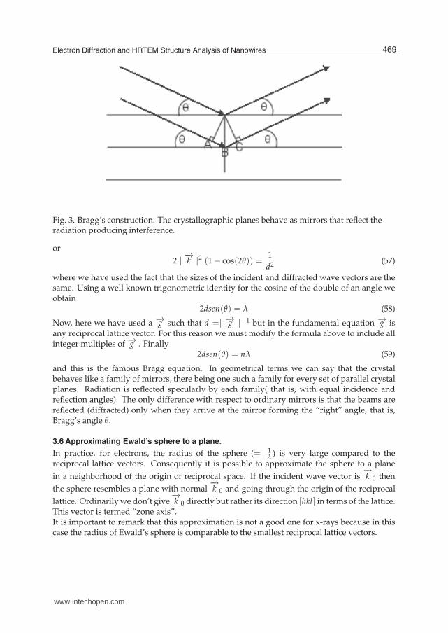
3.5 Bragg’s law
There is a very simple way of visualizing the fundamental diffraction equation. In figure 3 weshow schematically a family of planes that have a distance d (“interplanar distance”).Call −→g the reciprocal lattice vector that is normal to these planes and, as we have already seen,
it satisfies d =| −→g |−1. We also show (as arrows) the wave vectors−→k 0 and
−→k of the incident
and diffracted waves. From the figure one can see that the angle θ between−→k 0 and any plane
is the same as the angle between−→k and the planes. This angle is called “Bragg angle”.
Since −→g = (−→k −
−→k 0) , taking the dot product of the equation with itself; we have that
|−→k |2 + |
−→k 0 |2 −2
−→k ·
−→k 0 =| −→g |2 (56)
468 Nanowires - Fundamental Research
www.intechopen.com
Electron Diffraction and HRTEM Structure Analysis of Nanowires 9
Fig. 3. Bragg’s construction. The crystallographic planes behave as mirrors that reflect theradiation producing interference.
or
2 |−→k |2 (1 − cos(2θ)) =
1
d2(57)
where we have used the fact that the sizes of the incident and diffracted wave vectors are thesame. Using a well known trigonometric identity for the cosine of the double of an angle weobtain
2dsen(θ) = λ (58)
Now, here we have used a −→g such that d =| −→g |−1 but in the fundamental equation −→g isany reciprocal lattice vector. For this reason we must modify the formula above to include allinteger multiples of −→g . Finally
2dsen(θ) = nλ (59)
and this is the famous Bragg equation. In geometrical terms we can say that the crystalbehaves like a family of mirrors, there being one such a family for every set of parallel crystalplanes. Radiation is reflected specularly by each family( that is, with equal incidence andreflection angles). The only difference with respect to ordinary mirrors is that the beams arereflected (diffracted) only when they arrive at the mirror forming the “right” angle, that is,Bragg’s angle θ.
3.6 Approximating Ewald’s sphere to a plane.
In practice, for electrons, the radius of the sphere (= 1λ ) is very large compared to the
reciprocal lattice vectors. Consequently it is possible to approximate the sphere to a plane
in a neighborhood of the origin of reciprocal space. If the incident wave vector is−→k 0 then
the sphere resembles a plane with normal−→k 0 and going through the origin of the reciprocal
lattice. Ordinarily we don’t give−→k 0 directly but rather its direction [hkl] in terms of the lattice.
This vector is termed “zone axis”.It is important to remark that this approximation is not a good one for x-rays because in thiscase the radius of Ewald’s sphere is comparable to the smallest reciprocal lattice vectors.
469Electron Diffraction and HRTEM Structure Analysis of Nanowires
www.intechopen.com

10 Will-be-set-by-IN-TECH
3.7 An example
Consider an FCC crystal and assume the beam is along the [001]. A reciprocal lattice point(uvw) will contribute to the diffraction pattern if it satisfies
[001] · (uvw) = 0 (60)
The smallest vectors satisfying this equation and that also satisfying the condition that all ofthe indices are even or all of them are odd are (200) and (020) so the diffraction pattern willconsist of all the integer combinations of these vectors.
4. Higher order Laue zones
For a given zone axis [hkl] the planes
[hkl](uvw) = 0 (61)
give, as indicated above, the diffraction pattern. But sometimes other reciprocal lattice planesalso contribute to the pattern, and they are called “higher order Laue zones” (HOLZ) . Theymay arise as a result of having a very thin crystal or as a result of having an incomplete numberof layers in a given crystallographic direction. The ordinary case z = 0 is termed “zeroth orderLaue zone” or ZOLZ.Whatever the physical origin of these “forbidden spots”, their geometry can be calculated forcubic crystals in two equivalent ways:
1. Calculate the various reciprocal lattice planes by means of
[hkl](uvw) = n (62)
where n is an integer. Then project the resulting points onto the zeroth-order Laue Zone[hkl](uvw) = 0. Here [hkl] is the direction of the incoming beam.
2. Calculate the lattice plane(u′v′w′)[h′k′ l ′] = 0 (63)
where now (u′v′w′) is a vector parallel to the incoming beam. Then calculate the(two-dimensional) lattice reciprocal to the lattice plane.
Both approaches give the same answer. The second method calculates a projection inreciprocal space that is reciprocal to a section in real space. Thus we have a particular instanceof the well known section-projection theorem of Fourier theory.In the previous equations we are using the convention that [hkl] = ka + kb + lc where a, b, care lattice basis vectors and (uvw) = ua∗ + vb∗ + wc∗ where a∗, b∗, c∗ are the correspondingreciprocal lattice basis vectors.However the second approach has several advantages:
• no need to solve for several values of n. In fact, all the values of n are taken into account.
• No need to calculate projections at all, ZOLZ indices being automatically provided.
• Lends itself to the simple interpretation to be discussed below.
The practical procedure can be briefly summarized as:
470 Nanowires - Fundamental Research
www.intechopen.com

Electron Diffraction and HRTEM Structure Analysis of Nanowires 11
• If you know the beam is along the direction [hkl] then determine the vector (u′v′w′) inthe same direction (in the examples below this is very simple since a cubic lattice and itsreciprocal lattice differ only in size).
• Determine basis vectors a and b for the section (u′v′w′)[h′k′ l ′] = 0 (a Diophantine equationto be solved by standard methods).
• The reciprocal lattice vectors a∗and b∗can be determined from
a∗ =| b |2 a − (a · b)b
| a |2| b |2 −(a · b)2(64)
b∗ =| a |2 b − (a · b)a
| a |2| b |2 −(a · b)2(65)
and all the integer combinations of them give all the allowed and forbidden spots.
4.1 An example
For instance, in the FCC (112) zone the equation to solve is
(112)[hkl] = 0 (66)
whose solutions can be determined in many ways, possibly the easiest is by inspection so
a =1
2[110] (67)
b = [111] (68)
and
a∗ = 2a = (110) (69)
b∗ =b
3=
(111)
3(70)
(here we take advantage of the self reciprocity of cubic lattices). Notice that one of the pointsin the pattern is
a∗ − b∗ =(241)
3(71)
a “forbidden” spot actually being observed.Diffraction spots (allowed or forbidden) are expected at
g = m(110) +n(111)
3(72)
with m and n being integers.
5. Twinning
A twin is an aggregation of several crystals of the same species whose relative orientationsfollow well-defined laws. These orientations are related by symmetry operations which donot belong to the crystal class of the untwinned crystal, either by a rotation about an axis
471Electron Diffraction and HRTEM Structure Analysis of Nanowires
www.intechopen.com

12 Will-be-set-by-IN-TECH
[uvw] or by reflection by a lattice plane (hkl). The symmetry of the twin is generally higherthan that of the untwinned crystal.Two main kinds of twinning are distinguished, depending on whether the symmetryoperation is: (a) 180◦ rotation about an axis, called the twin axis, or (b) a reflection acrossa plane, called the twin plane.
5.1 Mirrors
Let P be a vector and P′ its image after reflection by a mirror that has N as a normal. Then itcan be easily shown that
P′ = P −P · N
| N |2N (73)
For instance, in an FCC crystal, if N = (111) and the crystal is P = [100] oriented withrespect to the incoming electron beam, the twin will be another crystal but oriented alongP′ = [100] − 1
3 [111] = 13 [211] or, simply [211]. In this way the diffraction patterns of the
twins can be computed.
6. Effect of incomplete layers
Consider an FCC lattice. The smallest vectors in the (111) plane are
a =1
2[110]
b =1
2[101]
(the 12 factor come from the fact that the standard unit cell is not primitive) and the lattice
reciprocal to the 2 dimensional lattice spanned by a and b is the one spanned by
a∗ =1
2[224] (74)
b∗ =1
2[242] (75)
so “kinematically forbidden” spots will appear.In the lattice there are, however, other (111) planes, they are stacked in the sequenceABCABC.... A vector taking the (111) layer (A) to the next one (B) is given by c = [001],and a vector taking it to the third layer (C) is d = [002].For this reason, the amplitude of a diffraction spot
μ = αa∗ + βb∗ (76)
will be modulated by
Ψ = 1 + exp[2πi(μ · c)] + exp[2πi(μ · d)] (77)
= 1 + exp[2πi(−4α + 2β
3)] + exp[2πi(
−8α + 4β
3)] (78)
472 Nanowires - Fundamental Research
www.intechopen.com
Electron Diffraction and HRTEM Structure Analysis of Nanowires 13
and the amplitude will be zero when
− 4α + 2β ≡ 1 (mod 3) (79)
or− 4α + 2β ≡ 2 (mod 3) (80)
and these equations rule out the forbidden spots when the stacking is complete, in the sensethat it comprises a whole ABCABC...sequence.
7. Direct and reciprocal spaces
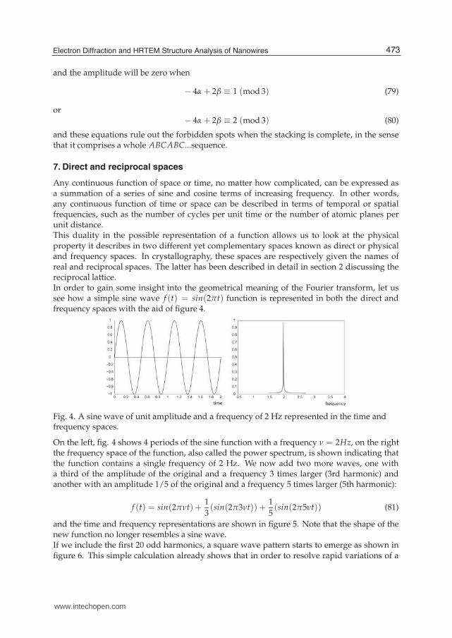
Any continuous function of space or time, no matter how complicated, can be expressed asa summation of a series of sine and cosine terms of increasing frequency. In other words,any continuous function of time or space can be described in terms of temporal or spatialfrequencies, such as the number of cycles per unit time or the number of atomic planes perunit distance.This duality in the possible representation of a function allows us to look at the physicalproperty it describes in two different yet complementary spaces known as direct or physicaland frequency spaces. In crystallography, these spaces are respectively given the names ofreal and reciprocal spaces. The latter has been described in detail in section 2 discussing thereciprocal lattice.In order to gain some insight into the geometrical meaning of the Fourier transform, let ussee how a simple sine wave f (t) = sin(2πt) function is represented in both the direct andfrequency spaces with the aid of figure 4.
Fig. 4. A sine wave of unit amplitude and a frequency of 2 Hz represented in the time andfrequency spaces.
On the left, fig. 4 shows 4 periods of the sine function with a frequency ν = 2Hz, on the rightthe frequency space of the function, also called the power spectrum, is shown indicating thatthe function contains a single frequency of 2 Hz. We now add two more waves, one witha third of the amplitude of the original and a frequency 3 times larger (3rd harmonic) andanother with an amplitude 1/5 of the original and a frequency 5 times larger (5th harmonic):
f (t) = sin(2πνt) +1
3(sin(2π3νt)) +
1
5(sin(2π5νt)) (81)
and the time and frequency representations are shown in figure 5. Note that the shape of thenew function no longer resembles a sine wave.If we include the first 20 odd harmonics, a square wave pattern starts to emerge as shown infigure 6. This simple calculation already shows that in order to resolve rapid variations of a
473Electron Diffraction and HRTEM Structure Analysis of Nanowires
www.intechopen.com

14 Will-be-set-by-IN-TECH
Fig. 5. The time and frequency space representations of a 2 Hz sine wave and its first twoodd harmonics (equation 81).
function, such as the sharp edges of a square wave, we need higher frequencies. The higherthe cut-off frequency, the better the approximation.
Fig. 6. The time and frequency space representations of the first 20 odd harmonics of a 2 Hzsine wave.
Since the sine is an odd function, i.e. sin(a) = −sin(−a), only odd functions can bereproduced by combinations of them. We could use cosines instead of sines in the expansion,but being even functions, i.e., cos(a) = cos(−a), they allow only the reproduction of evenfunctions. Since most functions are asymmetric (neither odd nor even) a combination of bothsines and cosines is needed to reproduce arbitrary functions. As a result, a general function oftime (or space) in one dimension can be expressed as
f (t) = a0 + a1cos(ωt) + a2cos(2ωt) + ... + b1sin(ωt) + b2sin(2ωt) + ... (82)
or, more succinctly:f (t) = Σ∞
i=0aicos(iωt) + Σ∞i=0bisin(iωt) (83)
where ω = 2πν and ai, bi are constants. In general, any non-periodic continuous functionf (x) of a single variable x can be expanded as
f (x) =∞
∑i=0
F(u)e2πixu (84)
where u is the temporal or spatial frequency variable and F(u) is given by
F(u) =∫ ∞
−∞f (x)e−2πixudx (85)
474 Nanowires - Fundamental Research
www.intechopen.com

Electron Diffraction and HRTEM Structure Analysis of Nanowires 15
In general, F(u) will be a complex quantity even though the original data are purely real. Themeaning of this is that not only the amplitude of each frequency present is important, but alsoits phase relationship to the others.Equation 84 is known as the Fourier transform of the function f (x) and equation 85 is theinverse transformation which is very similar except for the sign of the exponential term.The time (or space) and frequency representations of a function are equivalent in the sensethat besides size effects, they convey the same amount of information although they have verydifferent meanings. For our purposes, the most important property of the Fourier transformis that it relates the direct or physical space containing a crystal lattice and the reciprocal spacecontaining the reciprocal lattice and the kinematical diffraction pattern (see section 3).For an infinite crystal, the direct and reciprocal lattices are given in terms of each other by thethree dimensional form of equations 84 and 85. Since the size of real samples is always finite,this leads to important size and shape effects which become especially conspicuous in the caseof nanoparticles. In what follows we shall briefly describe what these effects are in order to beable to properly interpret a micro-diffraction pattern
8. Size and shape effects
We have already seen that the higher the frequencies in Fourier (diffraction) space, the moredetailed is the pattern in the physical space, the reason being that sharper features requiresmaller wavelengths to be reproduced. We shall further illustrate this property with the aid offig. 7 which also serves to illustrate the effect the specimen shape has on its diffraction pattern.Figure 7 shows the Fourier transform of a function which equals one inside the blacktriangular region shown on the left hand side and zero elsewhere. Note that the Fouriertransform has large spikes in the directions normal to the edges of the triangular regioncorresponding to the high frequency components needed to reproduce the sharp changes ofthe function at the boundaries of the triangle.
Fig. 7. Left: a triangular shape function which equals one inside the black triangle and zerooutside. Right: its Fourier transform rescaled for clarity.
The size of the specimen modifies the size of the diffraction pattern spots. The easiest wayto illustrate this is by calculating the Fourier transform of two waveforms of different length.Figure 8 shows the Fourier transform of the same function used in figure 5 (eq. 81) but using adifferent number of periods. Note that as the length of the waveform representing the size ofa crystal increases, the width of the spectral components decreases. In the limit, for an infinitewave, the Fourier peaks become Dirac delta functions.
475Electron Diffraction and HRTEM Structure Analysis of Nanowires
www.intechopen.com
16 Will-be-set-by-IN-TECH
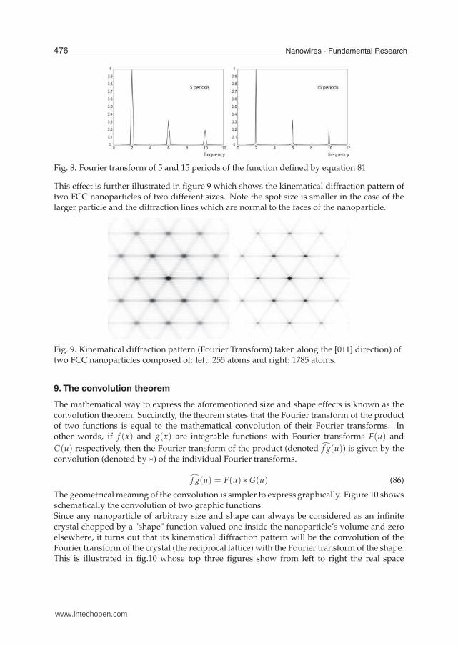
Fig. 8. Fourier transform of 5 and 15 periods of the function defined by equation 81
This effect is further illustrated in figure 9 which shows the kinematical diffraction pattern oftwo FCC nanoparticles of two different sizes. Note the spot size is smaller in the case of thelarger particle and the diffraction lines which are normal to the faces of the nanoparticle.
Fig. 9. Kinematical diffraction pattern (Fourier Transform) taken along the [011] direction) oftwo FCC nanoparticles composed of: left: 255 atoms and right: 1785 atoms.
9. The convolution theorem
The mathematical way to express the aforementioned size and shape effects is known as theconvolution theorem. Succinctly, the theorem states that the Fourier transform of the productof two functions is equal to the mathematical convolution of their Fourier transforms. Inother words, if f (x) and g(x) are integrable functions with Fourier transforms F(u) and
G(u) respectively, then the Fourier transform of the product (denoted f g(u)) is given by theconvolution (denoted by ∗) of the individual Fourier transforms.
f g(u) = F(u) ∗ G(u) (86)
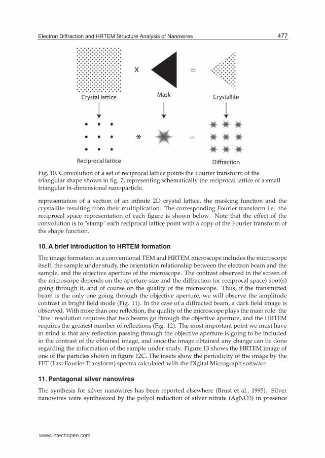
The geometrical meaning of the convolution is simpler to express graphically. Figure 10 showsschematically the convolution of two graphic functions.Since any nanoparticle of arbitrary size and shape can always be considered as an infinitecrystal chopped by a "shape" function valued one inside the nanoparticle’s volume and zeroelsewhere, it turns out that its kinematical diffraction pattern will be the convolution of theFourier transform of the crystal (the reciprocal lattice) with the Fourier transform of the shape.This is illustrated in fig.10 whose top three figures show from left to right the real space
476 Nanowires - Fundamental Research
www.intechopen.com
Electron Diffraction and HRTEM Structure Analysis of Nanowires 17
Fig. 10. Convolution of a set of reciprocal lattice points the Fourier transform of thetriangular shape shown in fig. 7, representing schematically the reciprocal lattice of a smalltriangular bi-dimensional nanoparticle.
representation of a section of an infinite 2D crystal lattice, the masking function and thecrystallite resulting from their multiplication. The corresponding Fourier transform i.e. thereciprocal space representation of each figure is shown below. Note that the effect of theconvolution is to "stamp" each reciprocal lattice point with a copy of the Fourier transform ofthe shape function.
10. A brief introduction to HRTEM formation
The image formation in a conventional TEM and HRTEM microscope includes the microscopeitself, the sample under study, the orientation relationship between the electron beam and thesample, and the objective aperture of the microscope. The contrast observed in the screen ofthe microscope depends on the aperture size and the diffraction (or reciprocal space) spot(s)going through it, and of course on the quality of the microscope. Thus, if the transmittedbeam is the only one going through the objective aperture, we will observe the amplitudecontrast in bright field mode (Fig. 11). In the case of a diffracted beam, a dark field image isobserved. With more than one reflection, the quality of the microscope plays the main role: the"line" resolution requires that two beams go through the objective aperture, and the HRTEMrequires the greatest number of reflections (Fig. 12). The most important point we must havein mind is that any reflection passing through the objective aperture is going to be includedin the contrast of the obtained image, and once the image obtained any change can be doneregarding the information of the sample under study. Figure 13 shows the HRTEM image ofone of the particles shown in figure 12C. The insets show the periodicity of the image by theFFT (Fast Fourier Transform) spectra calculated with the Digital Micrograph software.
11. Pentagonal silver nanowires
The synthesis for silver nanowires has been reported elsewhere (Brust et al., 1995). Silvernanowires were synthesized by the polyol reduction of silver nitrate (AgNO3) in presence
477Electron Diffraction and HRTEM Structure Analysis of Nanowires
www.intechopen.com

18 Will-be-set-by-IN-TECH
Fig. 11. A) Schematic representation of the size and position of the objective aperture in thefocal plane of the objective lens for image formation in a TEM in different situations: brightfield image (1), dark field image (2), line-resolution image (3) and high-resolution image (4).B) Bright field and C) dark field image of an Au particle.
of PVP. Scanning electron microscopy of the nanowires was conducted using the scanningelectron microscope (SEM) Hitachi 4500F. Transmission electron microscopy was conducted ina HRTEM JEOL 2010F microscope equipped with Schottky-type field emission gun, ultra-highresolution pole piece (Cs = 0.5mm), and a scanning transmission electron microscope (STEM)unit with high angle annular dark field (HAADF) detector operating at 200kV. For digitalimage processing the Digital Micrograph (GATAN) software was used. To simulate theelectron diffraction patterns, the SimulaTEM software (Gomez et al., 2010) was employed.Figure 14 shows the SEM images of the synthesized Ag nanowires where their pentagonalcross-section is presented.
Fig. 12. Example of a bright field image (A), two dark field images using a different reflectionin each case (B), and a high-resolution image (C) of Au nanoparticles.
12. Diffraction patterns and HRTEM images of pentagonal silver nanowires
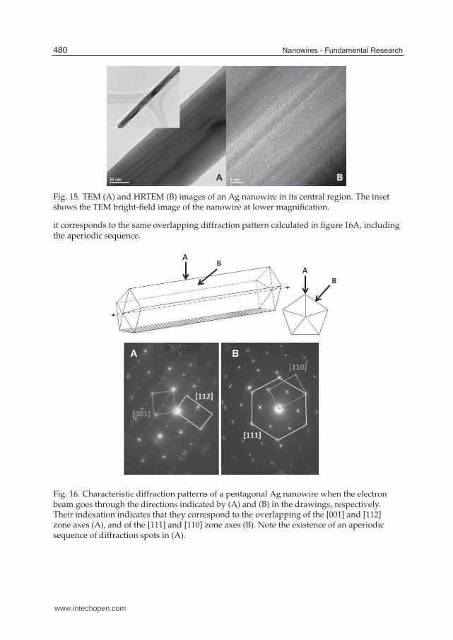
Once in the HRTEM microscope, conventional bright field (Fig. 15A) and HRTEM (Fig.15B) images and electron diffraction patterns of an Ag nanowire are obtained easily. Figure16 shows the electron diffraction patterns of an individual pentagonal Ag nanowire whenthe electron beam goes through the directions indicated by (A) and (B) in the drawings,respectively. Because the pentagonal rotational periodicity, there is an angle of 18◦ betweenthem. The analysis and indexation of these diffraction patterns indicate that they correspondto the overlapping of the [001] and [112] zone axes (Fig. 16A), and of the [111] and [110] zone
478 Nanowires - Fundamental Research
www.intechopen.com

Electron Diffraction and HRTEM Structure Analysis of Nanowires 19
Fig. 13. Magnification of the high-resolution image shown in figure 2C. The insets show theFFT spectra calculated with the Digital Micrograph software where the periodicity obtaineden each region of the Au nanoparticle is shown.
axes (Fig. 6B), of the silver FCC unit cell, respectively. The presence of an aperiodic sequenceof diffraction spots, mainly in figure 16 A is of notorious relevance.
Fig. 14. SEM images of the synthesized Ag nanowires showing their pentagonalcross-section.
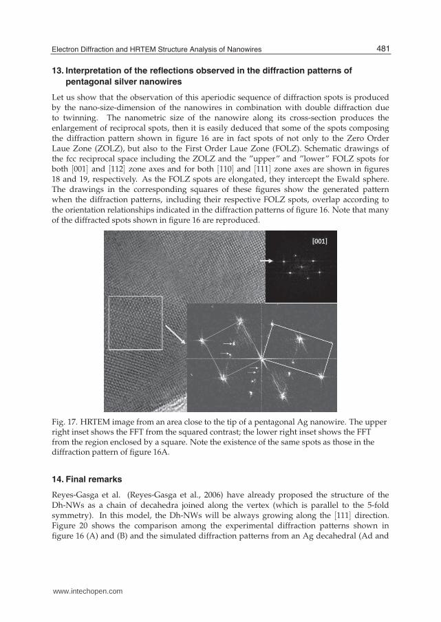
In order to understand the contrast observed in the HRTEM images of the pentagonal Agnanowires is quite important to know their structure. A HRTEM image from the area close tothe tip is shown in figure 17. The upper right inset shows the FFT from the indicated squaredcontrast, which corresponds to the [001] zone axis. The lower right inset shows the FFT fromthe region enclosed by the square in the HRTEM image. The analysis of this FFT indicates that
479Electron Diffraction and HRTEM Structure Analysis of Nanowires
www.intechopen.com
20 Will-be-set-by-IN-TECH
Fig. 15. TEM (A) and HRTEM (B) images of an Ag nanowire in its central region. The insetshows the TEM bright-field image of the nanowire at lower magnification.
it corresponds to the same overlapping diffraction pattern calculated in figure 16A, includingthe aperiodic sequence.
Fig. 16. Characteristic diffraction patterns of a pentagonal Ag nanowire when the electronbeam goes through the directions indicated by (A) and (B) in the drawings, respectively.Their indexation indicates that they correspond to the overlapping of the [001] and [112]zone axes (A), and of the [111] and [110] zone axes (B). Note the existence of an aperiodicsequence of diffraction spots in (A).
480 Nanowires - Fundamental Research
www.intechopen.com
Electron Diffraction and HRTEM Structure Analysis of Nanowires 21
13. Interpretation of the reflections observed in the diffraction patterns of
pentagonal silver nanowires
Let us show that the observation of this aperiodic sequence of diffraction spots is producedby the nano-size-dimension of the nanowires in combination with double diffraction dueto twinning. The nanometric size of the nanowire along its cross-section produces theenlargement of reciprocal spots, then it is easily deduced that some of the spots composingthe diffraction pattern shown in figure 16 are in fact spots of not only to the Zero OrderLaue Zone (ZOLZ), but also to the First Order Laue Zone (FOLZ). Schematic drawings ofthe fcc reciprocal space including the ZOLZ and the ”upper” and ”lower” FOLZ spots forboth [001] and [112] zone axes and for both [110] and [111] zone axes are shown in figures18 and 19, respectively. As the FOLZ spots are elongated, they intercept the Ewald sphere.The drawings in the corresponding squares of these figures show the generated patternwhen the diffraction patterns, including their respective FOLZ spots, overlap according tothe orientation relationships indicated in the diffraction patterns of figure 16. Note that manyof the diffracted spots shown in figure 16 are reproduced.
Fig. 17. HRTEM image from an area close to the tip of a pentagonal Ag nanowire. The upperright inset shows the FFT from the squared contrast; the lower right inset shows the FFTfrom the region enclosed by a square. Note the existence of the same spots as those in thediffraction pattern of figure 16A.
14. Final remarks
Reyes-Gasga et al. (Reyes-Gasga et al., 2006) have already proposed the structure of theDh-NWs as a chain of decahedra joined along the vertex (which is parallel to the 5-foldsymmetry). In this model, the Dh-NWs will be always growing along the [111] direction.Figure 20 shows the comparison among the experimental diffraction patterns shown infigure 16 (A) and (B) and the simulated diffraction patterns from an Ag decahedral (Ad and
481Electron Diffraction and HRTEM Structure Analysis of Nanowires
www.intechopen.com

22 Will-be-set-by-IN-TECH
Fig. 18. . Schematic drawing of the fcc reciprocal space along the [001] and [112] zone axesincluding the ZOLZ and the ”upper” and ”lower” FOLZ spots. The patterns have beenindexed accordingly. The square (A) shows the generated pattern when these patternsoverlap according to the orientation relationships indicated in figure 16A.
Fig. 19. Schematic drawing of the fcc reciprocal space along the [110] and [111] zone axesincluding the ZOLZ and the ”upper” and ”lower” FOLZ spots. The patterns have beenindexed accordingly. The square (B) shows the generated pattern when these patternsoverlap according to the orientation relationships indicated in figure 16B.
Bd) and an Ag elongated decahedron (Aed)) and (Bed). Note that the aperiodic sequenceobserved in the experimental patterns is reproduced in the case of the decahedron, whilethe elongated model generates a different aperiodic sequence. This idea of the chain ofdecahedra joined along the vertex has been successfully used in the analysis and interpretationof diffraction patterns of Au nanoparticles (Reyes-Gasga et al., 2008; Romeu & Reyes-Gasga,2002). However, observing the simulated patterns shown in figure 20, we conclude that thereis still a lot of work to be done in this direction.
482 Nanowires - Fundamental Research
www.intechopen.com

Electron Diffraction and HRTEM Structure Analysis of Nanowires 23
Fig. 20. Comparison among the experimental diffraction patterns shown in figure 16 (A) and(B) and the simulated diffraction patterns from an Ag decahedral (Ad and Bd) and an Agelongated decahedron (Aed and Bed).
15. Acknowledgements
We are grateful to Prof. Dr. M. Jose Yacaman, Dr. J. L. Elechiguerra, and Dr. Xiaoxia Gaofor supplying the samples used in this work and for their collaboration as coauthors of jointpapers. We also thank S. Tehuacanero-Nuñez, P. Mexia-Hernández, R. Hernandez-Reyes, J.Cañetas and M. Monroy-Escamilla for their technical support in the elaboration of this work.
16. References
Brust, M.; Fink, J.; Bethell, D.; Schiffring D. J. & Kiely, C. (1995). Synthesis and reactions offunctionalized gold nanoparticles. J. Chem. Soc. Chem. Comm. , 1655, Issue 16. DOI:10.1039/C39950001655.
Chen, H.; Gao, Y.; Zhang, H.; Liu, L.; Yu, H.; Tian, H.; Xie, S. & Li, J. (2004).Transmission-electron-microscopy study on fivefold twinned silver nanorods. J. Phys.Chem. B., Vol.108, No. 32, (August 2004), pp 12038-12043.
Gao, Y.; Jiang, P.; Lui, D. F.; Yuan, H. J.; Yan, X. Q.; Zhou, Z. P.; Wang, J. X.; Song, L.; Liu, L. F.;Zhou, W. Y.; Wang, G.; Wang, C. Y. & Xie, S. (2003). Synthesis, characterization andself-assembly of silver nanowires. Chem. Phys. Lett., Vol.380, No. 1-2, (October 2003),pp 146-149.
Giersig, M.; Pastoriza-Santos, I.; & Liz-Marzán L. M. (2004). Evidence of an aggregativemechanism during the formation of silver nanowires in N,N-dimethylformamide J.Mater. Chem., Vol.14, No. 4 (April 2004), pp 607-611.
Heinemann, K.; Yacamán, M. J.; Yang, C. Y. & Poppa, H. (1979). The structure of small,vapor-deposited particles: I. Experimental study of single crystals and particles withpentagonal profiles. J. Crystal Growth, Vol.47, No. 2, (August 1979), pp 177-186.
Hofmeister, H.; Nepijko, S. A.; Levlev, N. N.; Schulze, W.; & Ertl. G. (2002). Composition andlattice structure of fivefold twinned nanorods of silver. J. Crystal Growth, Vol.234, No.4, (February 2002), pp 773-781.
Howie A. & Marks, L. D. (1984). Elastic strains and energy balance for multiply twinnedparticles Phil. Mag., A Vol.49, No. 1 (January 1984), pp 95-109.
483Electron Diffraction and HRTEM Structure Analysis of Nanowires
www.intechopen.com

24 Will-be-set-by-IN-TECH
Reyes-Gasga, J.; Elechiguerra, J. L.; Liu, C.; Camacho-Bragado, A.; Montejano-Carrizales,J. M. & Yacamán, M. J. (2006). On the structure of nanorods and nanowires withpentagonal cross-sections. J. Cryst. Growth, Vol.286, No. 1, (January 2006), pp 162-172.
Reyes-Gasga, J.; Gómez-Rodríguez, A.; Gao, X. & José-Yacamán, M. (2008). Ultramicroscopy,Vol.108, No. 9, (August 2008), pp 929-936
Romeu, L.D. & Reyes-Gasga, J. (2011). Interpretation of the nano-electron-diffraction patternsalong the five-fold axis of decahedral gold nanoparticles. Microc.Microanal, Vol.17, inpress. DOI 10.1017/s1431927610094511.
Sun, Y.; Gates, B.; Mayers, B. & Xia, Y. (2002). Crystalline silver nanowires by soft solutionprocessing. Nanoletters, Vol.2, No. 2, (February 2002), pp 165-168.
Sun, Y.; Mayers, B.; Herricks T. & Xia, Y. (2003). Polyol synthesis of uniform silver nanowires:a plausible growth mechanism and the supporting evidence. Nanoletters, Vol.3, No.7, (July 2003), pp 955-960.
Zhao, Q.; Qiu, J.; Zhao, C.; Hou L. & Zhu, C. (2005). Synthesis and formation mechanism ofsilver nanowires by a templateless and seedless method Chem. Letters, Vol.34, No. 1,(January 2005), pp 30-31.
484 Nanowires - Fundamental Research
www.intechopen.com

Nanowires - Fundamental ResearchEdited by Dr. Abbass Hashim
ISBN 978-953-307-327-9Hard cover, 552 pagesPublisher InTechPublished online 19, July, 2011Published in print edition July, 2011
InTech EuropeUniversity Campus STeP Ri Slavka Krautzeka 83/A 51000 Rijeka, Croatia Phone: +385 (51) 770 447 Fax: +385 (51) 686 166www.intechopen.com
InTech ChinaUnit 405, Office Block, Hotel Equatorial Shanghai No.65, Yan An Road (West), Shanghai, 200040, China
Phone: +86-21-62489820 Fax: +86-21-62489821
Understanding and building up the foundation of nanowire concept is a high requirement and a bridge to newtechnologies. Any attempt in such direction is considered as one step forward in the challenge of advancednanotechnology. In the last few years, InTech scientific publisher has been taking the initiative of helpingworldwide scientists to share and improve the methods and the nanowire technology. This book is one ofInTech’s attempts to contribute to the promotion of this technology.
How to referenceIn order to correctly reference this scholarly work, feel free to copy and paste the following:
David Romeu, Alfredo Gomez and Jose Reyes-Gasga (2011). Electron Diffraction and HRTEM StructureAnalysis of Nanowires, Nanowires - Fundamental Research, Dr. Abbass Hashim (Ed.), ISBN: 978-953-307-327-9, InTech, Available from: http://www.intechopen.com/books/nanowires-fundamental-research/electron-diffraction-and-hrtem-structure-analysis-of-nanowires

© 2011 The Author(s). Licensee IntechOpen. This chapter is distributedunder the terms of the Creative Commons Attribution-NonCommercial-ShareAlike-3.0 License, which permits use, distribution and reproduction fornon-commercial purposes, provided the original is properly cited andderivative works building on this content are distributed under the samelicense.