electron beam doping in substrates of overlayer si/substrate gaas, sigaasp and evaporated gesi
TRANSCRIPT

~74 Nuclear Instruments and Methods in Physics Research B21 (1987) 574-575 North-Holland, Amsterdam
E L E C T R O N B E A M D O P I N G I N S U B S T R A T E S O F O V E R L A Y E R S i / S U B S T R A T E GaAs ,
Si/GaAsP AND EVAPORATED G e / S i
T a k a o W A D A 1) and M i c h i h i k o T A K E D A 2)
t~Department of Electrical and Computer Engineering, Nagoya Institute of Technology. Gokiso, Showa, Nagoya, Japan -')Gooernment Industrial Research Institute, Nagoya, Hirate. Kita, Nagoya, Japan
7 MeV electrons were used to introduce impurity Si atoms into GaAs (GaAsP) wafers from Si sheets, which were in contact with a GaAs (GaAsP) surface. Concentration-dependent diffusivities, D(c), at 120-200 o C were obtained to be - 10-17-10-12 cm 2 s-l. The values of D(c) decreased with increasing impurity concentration c. After Ge layers of - 0.11 /.tin thick were deposited by vacuum evaporation on the silicon wafers at room temperature, the Ge surfaces were exposed with a fluence of - 10 ~s electronscm-2 at - 200 ° C. The values of D(c) and C O from the Ge impurity concentration profile in Si were estimated to be - 10-17-2 X 1 0 -15
cm 2 s -1 and - 1022 cm -3, respectively. This value of C O was about thirty times as large as that in the similar experiments for the impurity sheet and the substrates.
1. Introduction
The properties of semiconductors irradiated by high energy electrons have been reported by many workers [1,2]. It is well known that ion implantation in semicon- ductors is accompanied by severe radiation damage introduced with the implantation process [3].
The method of electron beam doping in semiconduc- tors was discovered by one of the authors (T.W.) [4-7].
In the present paper the introduction of Si impurities into GaAsP (GaAs) in hot (120-200°C) irradiation is investigated.
Ge layers deposited by vacuum evaporation on the silicon wafers also were used for electron beam doping.
2. Experimental procedure
The samples used in the experiments were p-St (B- doped (111), - 2 5 - 5 0 ~2cm), GaAs (Cr-doped (100), l 0 s ~2cm) and n-GaAsl_xP x ( t = 2 5 /~m ( x = 0 . 4 ) , graded layer t = 40/Lm, Te: 10 t7 cm-3) . The surfaces of the Si impurity sheets (t = 0.27 and 0.35 ram) in contact with the GaAsP (GaAs) wafer (area 5 x 5 mm 2) were bombarded with a total fluence of about (5-10) × 1017 electrons cm- 2 at 7 MeV from an electron linear acceler- ator (fig. la) , with a pulse width of - 3.5 p.s, a 200 Hz duty cycle, and an average electron beam current of 40 p.Acm -2. During irradiation in air, the samples were air-cooled by a blower, as shown in fig. lb. The temper- atures of a sample heated by the irradiation were mea- sured by a thermocouple. The control of the irradiation temperature was done in air at a distance (20-25 cm)
0168-583X/87/$03.50 © Elsevier Science Publishers B.V. (Nor th-Hol land Physics Publishing Division)
a l ' - l l ' - I ,,-,M,v,
t I I Impurity sheet f I I Substrate
/ I
F / / / / 1
I / / I Blower
Linac / I
11"-1 V/// , I Stit
,,...._........-~ Sa m p I e Thermocouple
~ Beam collector
,~Ammeter
Fig. 1. (a) Schematic diagram of electron beam doping. (b) Schematic diagram of electron bombardment at 120-200 ° C.
from a beam exit window (titanium, t = 50 gm) of the electron linear accelerator to the sample, because with increasing the distance the current density of the elec- tron beam in the sample decreases due to energy loss and multiple scattering in the air layer and the window materials.
T. Wada, M. Takeda / Electron beam doping 575
3 . E x p e r i m e n t a l r e s u l t s a n d d i s c u s s i o n
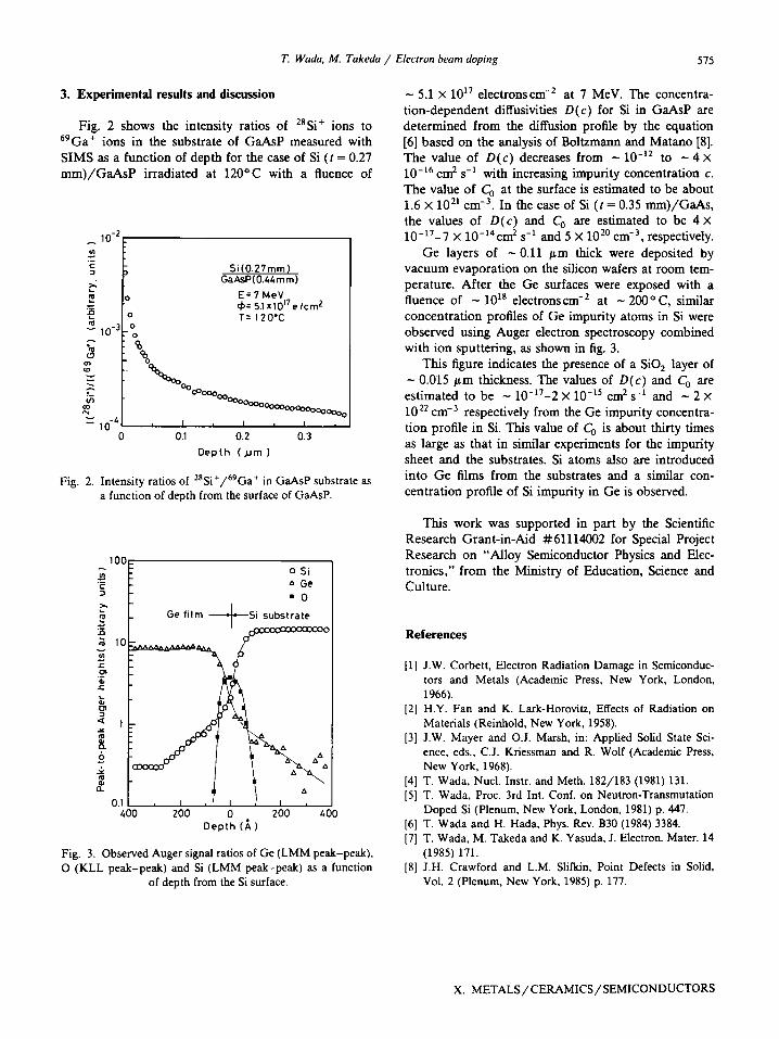
Fig. 2 shows the intensity ratios of 28Si+ ions to 69Ga+ ions in the substrate of GaAsP measured with SIMS as a function of depth for the case of Si (t = 0.27 m m ) / G a A s P irradiated at 120°C with a fluence of
A 1 0 - 2
c
~ lO-2
U'I
_~ 10-4 o
Si(0.27mm) GaAsP(O.44mrn)
E = 7 MeV qb= 5.1 x10¹⁷ e/crn 2 T: 120"C
o - o
iS
, I , ° ° ° l , __OOOoooot~ao °OOOooooon _ _
0.1 0.2 0.3 Depth (A im)
Fig. 2. Intensity ratios of 28Si+/69Ga + in GaAsP substrate as a function of depth from the surface of GaAsP.
1oo[
~ t ~ lO g r
e-
<
o Si A Ge = 0
/
Ge film ~ - S i substrate /
& O.t , I , I , 400 200 200 ~oo
Depth (A)
Fig. 3. Observed Auger signal ratios of Ge (LMM peak-peak), O (KLL peak-peak) and Si (LMM peak-peak) as a function
of depth from the Si surface.
- 5.1 X 10¹⁷ electronscm -2 at 7 MeV. The concentra- t ion-dependent diffusivities D(c) for Si in GaAsP are determined from the diffusion profile by the equation [6] based on the analysis of Boltzmann and Matano [8]. The value of D ( c ) decreases from - 1 0 -12 to - 4 x 10 -16 cm 2 s -1 with increasing impurity concentration c. The value of C o at the surface is estimated to be about 1.6 × 10 21 cm -3. In (he case of Si (t = 0.35 m m ) / G a A s , the values of D(c ) and C o are estimated to be 4 x 10-17-7 × 10-14cm 2 s -1 and 5 x 10 2o cm -3, respectively.
Ge layers of - 0 . 1 1 /~m thick were deposited by vacuum evaporat ion on the silicon wafers at room tem- perature. After the Ge surfaces were exposed with a fluence of - 1 0 Is electronscm -2 at - 2 0 0 ° C , similar concentrat ion profiles of Ge impurity atoms in Si were observed using Auger electron spectroscopy combined with ion sputtering, as shown in fig. 3.
This figure indicates the presence of a SiO 2 layer of - 0.015 # m thickness. The values of D(c) and C o are estimated to be - 10-17-2 × 10 -15 cm 2 s -1 and - 2 x 10 22 cm -3 respectively from the Ge impurity concentra- tion profile in Si. This value of C O is about thirty times as large as that in similar experiments for the impurity sheet and the substrates. Si atoms also are introduced into Ge films from the substrates and a similar con- centration profile of Si impurity in Ge is observed.
This work was supported in part by the Scientific Research Grant- in-Aid *:61114002 for Special Project Research on "Al loy Semiconductor Physics and Elec- tronics," from the Ministry of Education, Science and Culture.
R e f e r e n c e s
[1] J.W. Corbett, Electron Radiation Damage in Semiconduc- tors and Metals (Academic Press, New York, London, 1966).
[2] H.Y. Fan and K. Lark-Horovitz, Effects of Radiation on Materials (Reinhold, New York, 1958).
[3] J.W. Mayer and O.J. Marsh, in: Applied Solid State Sci- ence, eds., C.J. Kriessman and R. Wolf (Academic Press, New York, 1968).
[4] T. Wada, Nucl. Instr. and Meth. 182/183 (1981) 131. [5] T. Wada, Proc. 3rd Int. Conf. on Neutron-Transmutation
Doped Si (Plenum, New York, London, 1981) p. 447. [6] T. Wada and H. Hada, Phys. Rev. B30 (1984) 3384. [7] T. Wada, M. Takeda and K. Yasuda, J. Electron. Mater. 14
(1985) 171. [8] J.H. Crawford and L.M. Slifldn, Point Defects in Solid,
Vol. 2 (Plenum, New York, 1985) p. 177.
X. METALS/CERAMICS/SEMICONDUCTORS