electron and spin transport through single molecules with scanning tunneling microscopy · ·...
TRANSCRIPT
C4.10 Wulfhekel
1
Subproject C4.10
Electron and Spin Transport through Single Molecules with Scanning Tunneling Microscopy
Principle Investigator: Wulf Wulfhekel CFN-Financed Scientists: Further Scientists: Annika Borg, Dr. Eric Bdeaurepaire, Dr. Martin Bowen, Prof. Dr. Ferdinand Evers, Dr. Alexej Bagrets, Prof. Dr. Mario Ruben, Dr. Frank Schramm Physikalisches Institut Karlsruhe Institute of Technology (KIT) Institut für Nanotechnologie Karlruhe Institute of Technology (KIT) IPCMS Strasbourg, France
C4.10 Wulfhekel
2
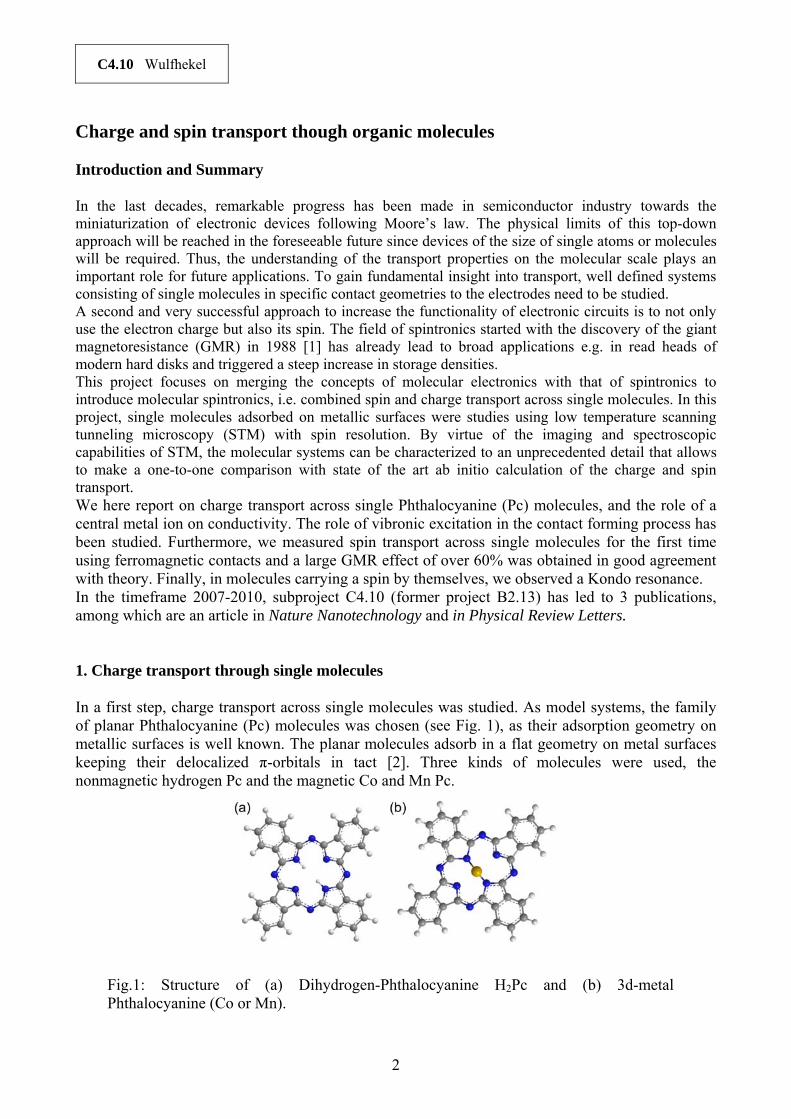
Charge and spin transport though organic molecules Introduction and Summary In the last decades, remarkable progress has been made in semiconductor industry towards the miniaturization of electronic devices following Moore’s law. The physical limits of this top-down approach will be reached in the foreseeable future since devices of the size of single atoms or molecules will be required. Thus, the understanding of the transport properties on the molecular scale plays an important role for future applications. To gain fundamental insight into transport, well defined systems consisting of single molecules in specific contact geometries to the electrodes need to be studied. A second and very successful approach to increase the functionality of electronic circuits is to not only use the electron charge but also its spin. The field of spintronics started with the discovery of the giant magnetoresistance (GMR) in 1988 [1] has already lead to broad applications e.g. in read heads of modern hard disks and triggered a steep increase in storage densities. This project focuses on merging the concepts of molecular electronics with that of spintronics to introduce molecular spintronics, i.e. combined spin and charge transport across single molecules. In this project, single molecules adsorbed on metallic surfaces were studies using low temperature scanning tunneling microscopy (STM) with spin resolution. By virtue of the imaging and spectroscopic capabilities of STM, the molecular systems can be characterized to an unprecedented detail that allows to make a one-to-one comparison with state of the art ab initio calculation of the charge and spin transport. We here report on charge transport across single Phthalocyanine (Pc) molecules, and the role of a central metal ion on conductivity. The role of vibronic excitation in the contact forming process has been studied. Furthermore, we measured spin transport across single molecules for the first time using ferromagnetic contacts and a large GMR effect of over 60% was obtained in good agreement with theory. Finally, in molecules carrying a spin by themselves, we observed a Kondo resonance. In the timeframe 2007-2010, subproject C4.10 (former project B2.13) has led to 3 publications, among which are an article in Nature Nanotechnology and in Physical Review Letters. 1. Charge transport through single molecules In a first step, charge transport across single molecules was studied. As model systems, the family of planar Phthalocyanine (Pc) molecules was chosen (see Fig. 1), as their adsorption geometry on metallic surfaces is well known. The planar molecules adsorb in a flat geometry on metal surfaces keeping their delocalized π-orbitals in tact [2]. Three kinds of molecules were used, the nonmagnetic hydrogen Pc and the magnetic Co and Mn Pc.
Fig.1: Structure of (a) Dihydrogen-Phthalocyanine H2Pc and (b) 3d-metal Phthalocyanine (Co or Mn).
C4.10 Wulfhekel
3
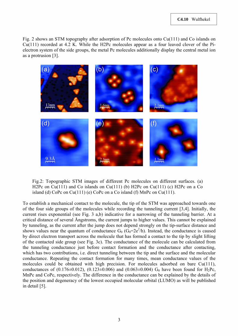
Fig. 2 shows an STM topography after adsorption of Pc molecules onto Cu(111) and Co islands on Cu(111) recorded at 4.2 K. While the H2Pc molecules appear as a four leaved clover of the Pi-electron system of the side groups, the metal Pc molecules additionally display the central metal ion as a protrusion [3].
Fig.2: Topographic STM images of different Pc molecules on different surfaces. (a) H2Pc on Cu(111) and Co islands on Cu(111) (b) H2Pc on Cu(111) (c) H2Pc on a Co island (d) CoPc on Cu(111) (e) CoPc on a Co island (f) MnPc on Cu(111).
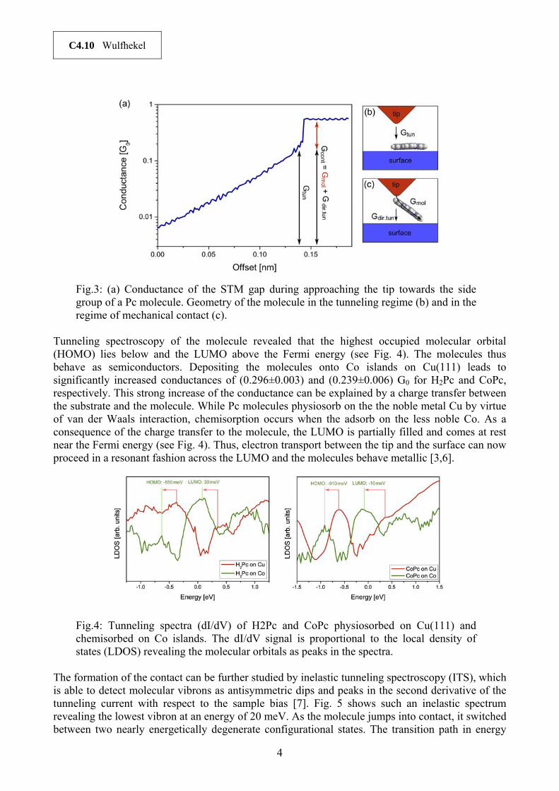
To establish a mechanical contact to the molecule, the tip of the STM was approached towards one of the four side groups of the molecules while recording the tunneling current [3,4]. Initially, the current rises exponential (see Fig. 3 a,b) indicative for a narrowing of the tunneling barrier. At a critical distance of several Ångstroms, the current jumps to higher values. This cannot be explained by tunneling, as the current after the jump does not depend strongly on the tip-surface distance and shows values near the quantum of conductance G0 (G0=2e2/h). Instead, the conductance is caused by direct electron transport across the molecule that has formed a contact to the tip by slight lifting of the contacted side group (see Fig. 3c). The conductance of the molecule can be calculated from the tunneling conductance just before contact formation and the conductance after contacting, which has two contributions, i.e. direct tunneling between the tip and the surface and the molecular conductance. Repeating the contact formation for many times, mean conductance values of the molecules could be obtained with high precision. For molecules adsorbed on bare Cu(111), conductances of (0.176±0.012), (0.123±0.006) and (0.063±0.004) G0 have been found for H2Pc, MnPc and CoPc, respectively. The difference in the conductance can be explained by the details of the position and degeneracy of the lowest occupied molecular orbital (LUMO) as will be published in detail [5].
C4.10 Wulfhekel
4
Fig.3: (a) Conductance of the STM gap during approaching the tip towards the side group of a Pc molecule. Geometry of the molecule in the tunneling regime (b) and in the regime of mechanical contact (c).
Tunneling spectroscopy of the molecule revealed that the highest occupied molecular orbital (HOMO) lies below and the LUMO above the Fermi energy (see Fig. 4). The molecules thus behave as semiconductors. Depositing the molecules onto Co islands on Cu(111) leads to significantly increased conductances of (0.296±0.003) and (0.239±0.006) G0 for H2Pc and CoPc, respectively. This strong increase of the conductance can be explained by a charge transfer between the substrate and the molecule. While Pc molecules physiosorb on the the noble metal Cu by virtue of van der Waals interaction, chemisorption occurs when the adsorb on the less noble Co. As a consequence of the charge transfer to the molecule, the LUMO is partially filled and comes at rest near the Fermi energy (see Fig. 4). Thus, electron transport between the tip and the surface can now proceed in a resonant fashion across the LUMO and the molecules behave metallic [3,6].
Fig.4: Tunneling spectra (dI/dV) of H2Pc and CoPc physiosorbed on Cu(111) and chemisorbed on Co islands. The dI/dV signal is proportional to the local density of states (LDOS) revealing the molecular orbitals as peaks in the spectra.
The formation of the contact can be further studied by inelastic tunneling spectroscopy (ITS), which is able to detect molecular vibrons as antisymmetric dips and peaks in the second derivative of the tunneling current with respect to the sample bias [7]. Fig. 5 shows such an inelastic spectrum revealing the lowest vibron at an energy of 20 meV. As the molecule jumps into contact, it switched between two nearly energetically degenerate configurational states. The transition path in energy
C4.10 Wulfhekel
5
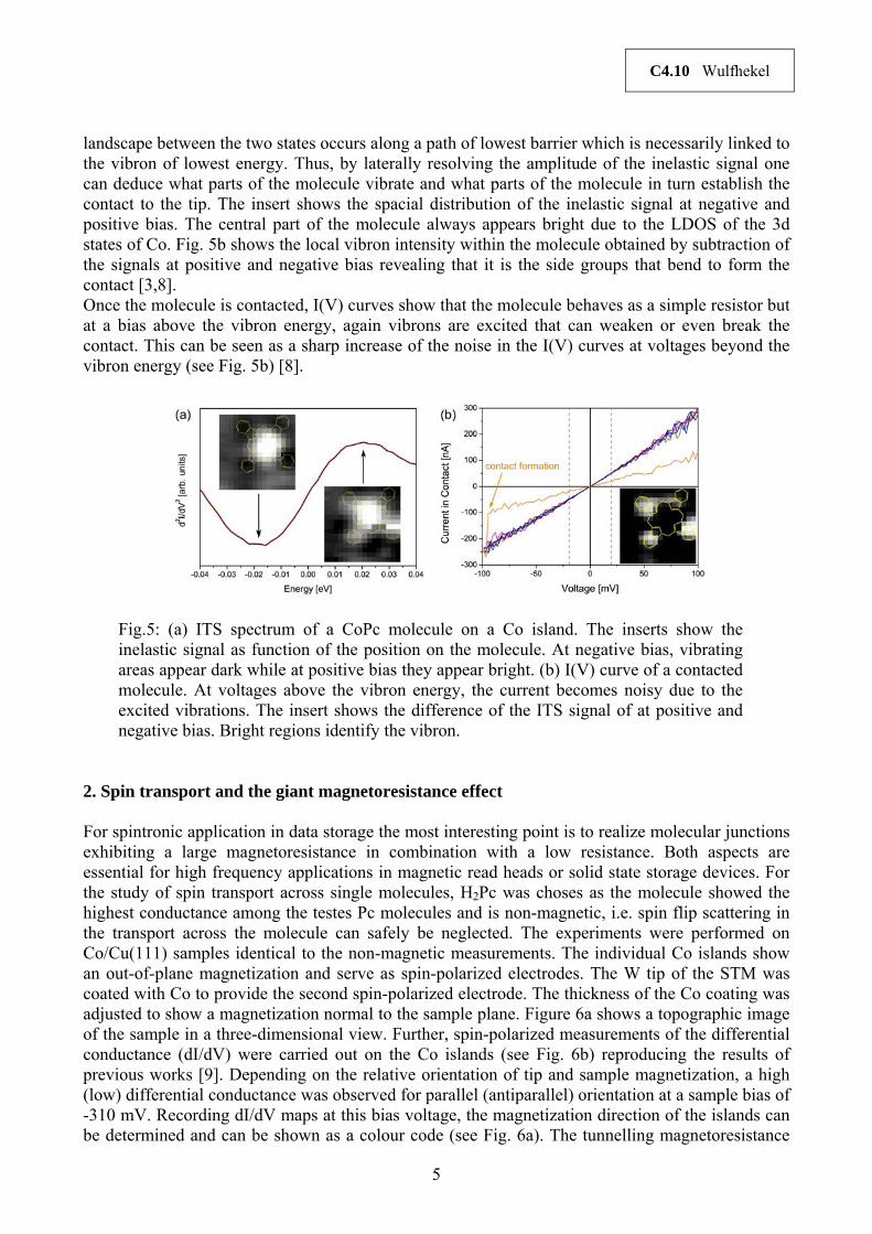
landscape between the two states occurs along a path of lowest barrier which is necessarily linked to the vibron of lowest energy. Thus, by laterally resolving the amplitude of the inelastic signal one can deduce what parts of the molecule vibrate and what parts of the molecule in turn establish the contact to the tip. The insert shows the spacial distribution of the inelastic signal at negative and positive bias. The central part of the molecule always appears bright due to the LDOS of the 3d states of Co. Fig. 5b shows the local vibron intensity within the molecule obtained by subtraction of the signals at positive and negative bias revealing that it is the side groups that bend to form the contact [3,8]. Once the molecule is contacted, I(V) curves show that the molecule behaves as a simple resistor but at a bias above the vibron energy, again vibrons are excited that can weaken or even break the contact. This can be seen as a sharp increase of the noise in the I(V) curves at voltages beyond the vibron energy (see Fig. 5b) [8].
Fig.5: (a) ITS spectrum of a CoPc molecule on a Co island. The inserts show the inelastic signal as function of the position on the molecule. At negative bias, vibrating areas appear dark while at positive bias they appear bright. (b) I(V) curve of a contacted molecule. At voltages above the vibron energy, the current becomes noisy due to the excited vibrations. The insert shows the difference of the ITS signal of at positive and negative bias. Bright regions identify the vibron.
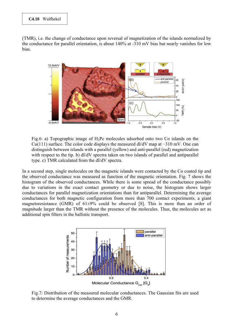
2. Spin transport and the giant magnetoresistance effect For spintronic application in data storage the most interesting point is to realize molecular junctions exhibiting a large magnetoresistance in combination with a low resistance. Both aspects are essential for high frequency applications in magnetic read heads or solid state storage devices. For the study of spin transport across single molecules, H2Pc was choses as the molecule showed the highest conductance among the testes Pc molecules and is non-magnetic, i.e. spin flip scattering in the transport across the molecule can safely be neglected. The experiments were performed on Co/Cu(111) samples identical to the non-magnetic measurements. The individual Co islands show an out-of-plane magnetization and serve as spin-polarized electrodes. The W tip of the STM was coated with Co to provide the second spin-polarized electrode. The thickness of the Co coating was adjusted to show a magnetization normal to the sample plane. Figure 6a shows a topographic image of the sample in a three-dimensional view. Further, spin-polarized measurements of the differential conductance (dI/dV) were carried out on the Co islands (see Fig. 6b) reproducing the results of previous works [9]. Depending on the relative orientation of tip and sample magnetization, a high (low) differential conductance was observed for parallel (antiparallel) orientation at a sample bias of -310 mV. Recording dI/dV maps at this bias voltage, the magnetization direction of the islands can be determined and can be shown as a colour code (see Fig. 6a). The tunnelling magnetoresistance
C4.10 Wulfhekel
6
(TMR), i.e. the change of conductance upon reversal of magnetization of the islands normalized by the conductance for parallel orientation, is about 140% at -310 mV bias but nearly vanishes for low bias.
Fig.6: a) Topographic image of H2Pc molecules adsorbed onto two Co islands on the Cu(111) surface. The color code displays the measured dI/dV map at −310 mV. One can distinguish between islands with a parallel (yellow) and anti-parallel (red) magnetization with respect to the tip. b) dI/dV spectra taken on two islands of parallel and antiparallel type. c) TMR calculated from the dI/dV spectra.
In a second step, single molecules on the magnetic islands were contacted by the Co coated tip and the observed conductance was measured as function of the magnetic orientation. Fig. 7 shows the histogram of the observed conductances. While there is some spread of the conductance possibly due to variations in the exact contact geometry or due to noise, the histogram shows larger conductances for parallel magnetization orientations than for antiparallel. Determining the average conductances for both magnetic configuration from more than 700 contact experiments, a giant magnetoresistance (GMR) of 61±9% could be observed [8]. This is more than an order of magnitude larger than the TMR without the presence of the molecules. Thus, the molecules act as additional spin filters in the ballistic transport.
Fig.7: Distribution of the measured molecular conductances. The Gaussian fits are used to determine the average conductances and the GMR.
C4.10 Wulfhekel
7
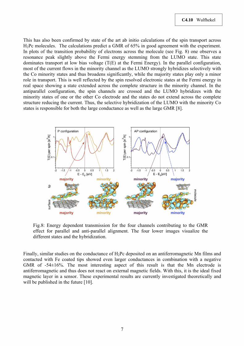
This has also been confirmed by state of the art ab initio calculations of the spin transport across H2Pc molecules. The calculations predict a GMR of 65% in good agreement with the experiment. In plots of the transition probability of electrons across the molecule (see Fig. 8) one observes a resonance peak slightly above the Fermi energy stemming from the LUMO state. This state dominates transport at low bias voltage (T(E) at the Fermi Energy). In the parallel configuration, most of the current flows in the minority channel as the LUMO strongly hybridizes selectively with the Co minority states and thus broadens significantly, while the majority states play only a minor role in transport. This is well reflected by the spin resolved electronic states at the Fermi energy in real space showing a state extended across the complete structure in the minority channel. In the antiparallel configuration, the spin channels are crossed and the LUMO hybridizes with the minority states of one or the other Co electrode and the states do not extend across the complete structure reducing the current. Thus, the selective hybridization of the LUMO with the minority Co states is responsible for both the large conductance as well as the large GMR [8].
Fig.8: Energy dependent transmission for the four channels contributing to the GMR effect for parallel and anti-parallel alignment. The four lower images visualize the different states and the hybridization.
Finally, similar studies on the conductance of H2Pc deposited on an antiferromagnetic Mn films and contacted with Fe coated tips showed even larger conductances in combination with a negative GMR of -54±16%. The most interesting aspect of this result is that the Mn electrode is antiferromagnetic and thus does not react on external magnetic fields. With this, it is the ideal fixed magnetic layer in a sensor. These experimental results are currently investigated theoretically and will be published in the future [10].
C4.10 Wulfhekel
8
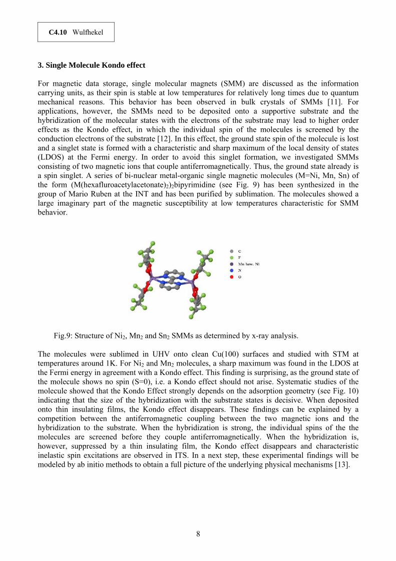
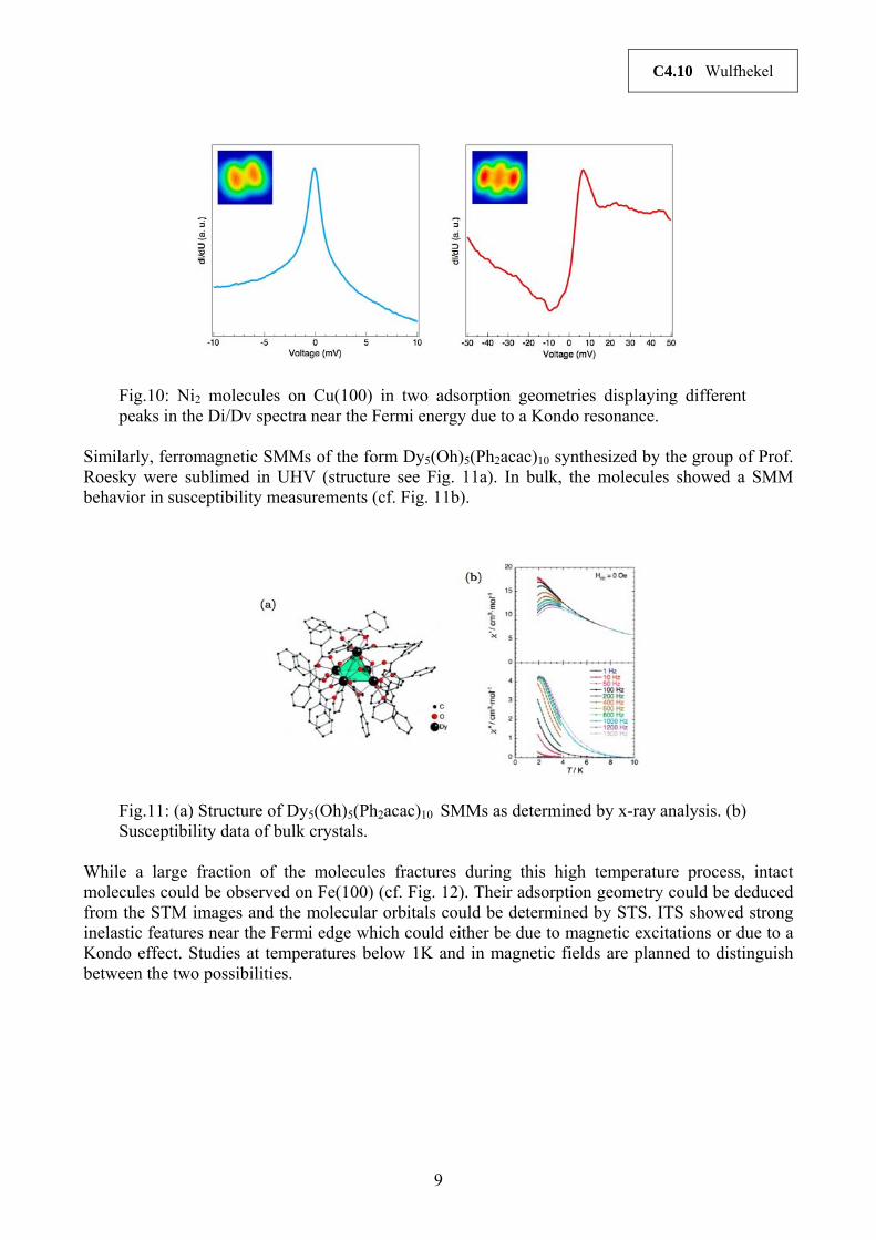
3. Single Molecule Kondo effect For magnetic data storage, single molecular magnets (SMM) are discussed as the information carrying units, as their spin is stable at low temperatures for relatively long times due to quantum mechanical reasons. This behavior has been observed in bulk crystals of SMMs [11]. For applications, however, the SMMs need to be deposited onto a supportive substrate and the hybridization of the molecular states with the electrons of the substrate may lead to higher order effects as the Kondo effect, in which the individual spin of the molecules is screened by the conduction electrons of the substrate [12]. In this effect, the ground state spin of the molecule is lost and a singlet state is formed with a characteristic and sharp maximum of the local density of states (LDOS) at the Fermi energy. In order to avoid this singlet formation, we investigated SMMs consisting of two magnetic ions that couple antiferromagnetically. Thus, the ground state already is a spin singlet. A series of bi-nuclear metal-organic single magnetic molecules (M=Ni, Mn, Sn) of the form (M(hexafluroacetylacetonate)2)2bipyrimidine (see Fig. 9) has been synthesized in the group of Mario Ruben at the INT and has been purified by sublimation. The molecules showed a large imaginary part of the magnetic susceptibility at low temperatures characteristic for SMM behavior.
Fig.9: Structure of Ni2, Mn2 and Sn2 SMMs as determined by x-ray analysis.
The molecules were sublimed in UHV onto clean Cu(100) surfaces and studied with STM at temperatures around 1K. For Ni2 and Mn2 molecules, a sharp maximum was found in the LDOS at the Fermi energy in agreement with a Kondo effect. This finding is surprising, as the ground state of the molecule shows no spin (S=0), i.e. a Kondo effect should not arise. Systematic studies of the molecule showed that the Kondo Effect strongly depends on the adsorption geometry (see Fig. 10) indicating that the size of the hybridization with the substrate states is decisive. When deposited onto thin insulating films, the Kondo effect disappears. These findings can be explained by a competition between the antiferromagnetic coupling between the two magnetic ions and the hybridization to the substrate. When the hybridization is strong, the individual spins of the the molecules are screened before they couple antiferromagnetically. When the hybridization is, however, suppressed by a thin insulating film, the Kondo effect disappears and characteristic inelastic spin excitations are observed in ITS. In a next step, these experimental findings will be modeled by ab initio methods to obtain a full picture of the underlying physical mechanisms [13].
C4.10 Wulfhekel
9
Fig.10: Ni2 molecules on Cu(100) in two adsorption geometries displaying different peaks in the Di/Dv spectra near the Fermi energy due to a Kondo resonance.
Similarly, ferromagnetic SMMs of the form Dy5(Oh)5(Ph2acac)10 synthesized by the group of Prof. Roesky were sublimed in UHV (structure see Fig. 11a). In bulk, the molecules showed a SMM behavior in susceptibility measurements (cf. Fig. 11b).
Fig.11: (a) Structure of Dy5(Oh)5(Ph2acac)10 SMMs as determined by x-ray analysis. (b) Susceptibility data of bulk crystals.
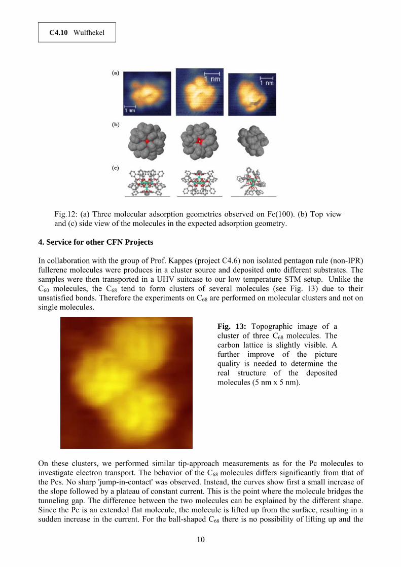
While a large fraction of the molecules fractures during this high temperature process, intact molecules could be observed on Fe(100) (cf. Fig. 12). Their adsorption geometry could be deduced from the STM images and the molecular orbitals could be determined by STS. ITS showed strong inelastic features near the Fermi edge which could either be due to magnetic excitations or due to a Kondo effect. Studies at temperatures below 1K and in magnetic fields are planned to distinguish between the two possibilities.
C4.10 Wulfhekel
10
Fig.12: (a) Three molecular adsorption geometries observed on Fe(100). (b) Top view and (c) side view of the molecules in the expected adsorption geometry.
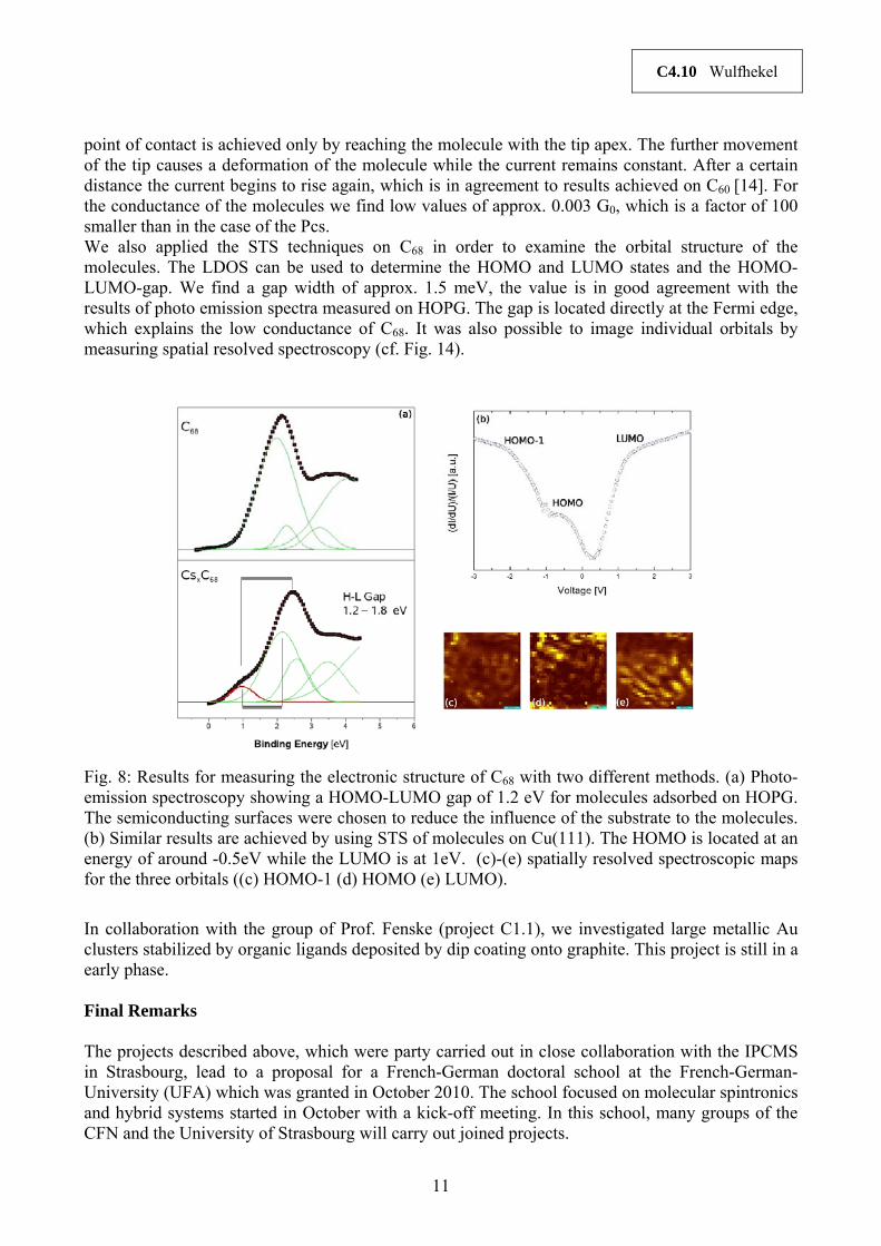
4. Service for other CFN Projects In collaboration with the group of Prof. Kappes (project C4.6) non isolated pentagon rule (non-IPR) fullerene molecules were produces in a cluster source and deposited onto different substrates. The samples were then transported in a UHV suitcase to our low temperature STM setup. Unlike the C60 molecules, the C68 tend to form clusters of several molecules (see Fig. 13) due to their unsatisfied bonds. Therefore the experiments on C68 are performed on molecular clusters and not on single molecules.
On these clusters, we performed similar tip-approach measurements as for the Pc molecules to investigate electron transport. The behavior of the C68 molecules differs significantly from that of the Pcs. No sharp 'jump-in-contact' was observed. Instead, the curves show first a small increase of the slope followed by a plateau of constant current. This is the point where the molecule bridges the tunneling gap. The difference between the two molecules can be explained by the different shape. Since the Pc is an extended flat molecule, the molecule is lifted up from the surface, resulting in a sudden increase in the current. For the ball-shaped C68 there is no possibility of lifting up and the
Fig. 13: Topographic image of acluster of three C68 molecules. Thecarbon lattice is slightly visible. Afurther improve of the picturequality is needed to determine thereal structure of the depositedmolecules (5 nm x 5 nm).
C4.10 Wulfhekel
11
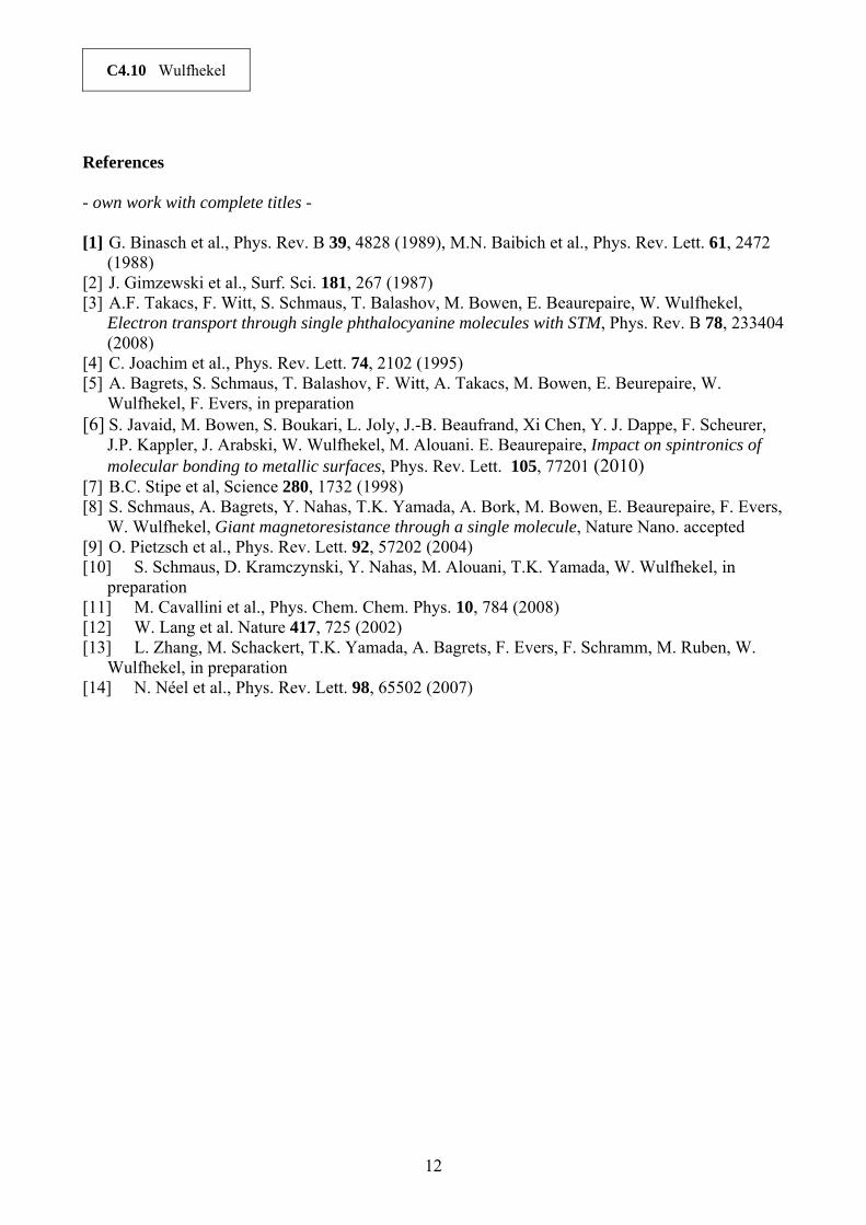
point of contact is achieved only by reaching the molecule with the tip apex. The further movement of the tip causes a deformation of the molecule while the current remains constant. After a certain distance the current begins to rise again, which is in agreement to results achieved on C60 [14]. For the conductance of the molecules we find low values of approx. 0.003 G0, which is a factor of 100 smaller than in the case of the Pcs. We also applied the STS techniques on C68 in order to examine the orbital structure of the molecules. The LDOS can be used to determine the HOMO and LUMO states and the HOMO-LUMO-gap. We find a gap width of approx. 1.5 meV, the value is in good agreement with the results of photo emission spectra measured on HOPG. The gap is located directly at the Fermi edge, which explains the low conductance of C68. It was also possible to image individual orbitals by measuring spatial resolved spectroscopy (cf. Fig. 14).
Fig. 8: Results for measuring the electronic structure of C68 with two different methods. (a) Photo- emission spectroscopy showing a HOMO-LUMO gap of 1.2 eV for molecules adsorbed on HOPG. The semiconducting surfaces were chosen to reduce the influence of the substrate to the molecules. (b) Similar results are achieved by using STS of molecules on Cu(111). The HOMO is located at an energy of around -0.5eV while the LUMO is at 1eV. (c)-(e) spatially resolved spectroscopic maps for the three orbitals ((c) HOMO-1 (d) HOMO (e) LUMO).
In collaboration with the group of Prof. Fenske (project C1.1), we investigated large metallic Au clusters stabilized by organic ligands deposited by dip coating onto graphite. This project is still in a early phase. Final Remarks The projects described above, which were party carried out in close collaboration with the IPCMS in Strasbourg, lead to a proposal for a French-German doctoral school at the French-German-University (UFA) which was granted in October 2010. The school focused on molecular spintronics and hybrid systems started in October with a kick-off meeting. In this school, many groups of the CFN and the University of Strasbourg will carry out joined projects.
C4.10 Wulfhekel
12
References - own work with complete titles - [1] G. Binasch et al., Phys. Rev. B 39, 4828 (1989), M.N. Baibich et al., Phys. Rev. Lett. 61, 2472
(1988) [2] J. Gimzewski et al., Surf. Sci. 181, 267 (1987) [3] A.F. Takacs, F. Witt, S. Schmaus, T. Balashov, M. Bowen, E. Beaurepaire, W. Wulfhekel,
Electron transport through single phthalocyanine molecules with STM, Phys. Rev. B 78, 233404 (2008)
[4] C. Joachim et al., Phys. Rev. Lett. 74, 2102 (1995) [5] A. Bagrets, S. Schmaus, T. Balashov, F. Witt, A. Takacs, M. Bowen, E. Beurepaire, W.
Wulfhekel, F. Evers, in preparation [6] S. Javaid, M. Bowen, S. Boukari, L. Joly, J.-B. Beaufrand, Xi Chen, Y. J. Dappe, F. Scheurer,
J.P. Kappler, J. Arabski, W. Wulfhekel, M. Alouani. E. Beaurepaire, Impact on spintronics of molecular bonding to metallic surfaces, Phys. Rev. Lett. 105, 77201 (2010)
[7] B.C. Stipe et al, Science 280, 1732 (1998) [8] S. Schmaus, A. Bagrets, Y. Nahas, T.K. Yamada, A. Bork, M. Bowen, E. Beaurepaire, F. Evers,
W. Wulfhekel, Giant magnetoresistance through a single molecule, Nature Nano. accepted [9] O. Pietzsch et al., Phys. Rev. Lett. 92, 57202 (2004) [10] S. Schmaus, D. Kramczynski, Y. Nahas, M. Alouani, T.K. Yamada, W. Wulfhekel, in
preparation [11] M. Cavallini et al., Phys. Chem. Chem. Phys. 10, 784 (2008) [12] W. Lang et al. Nature 417, 725 (2002) [13] L. Zhang, M. Schackert, T.K. Yamada, A. Bagrets, F. Evers, F. Schramm, M. Ruben, W.
Wulfhekel, in preparation [14] N. Néel et al., Phys. Rev. Lett. 98, 65502 (2007)