electromagnetics · engineering electromagnetics, nominally using vol. 1. however, the particular...
TRANSCRIPT

ELECTROMAGNETICSSTEVEN W. ELLINGSON
VOLUME 2

ELECTROMAGNETICS
VOLUME 2

Publication of this book was made possible in part by the Virginia Tech University Libraries’ Open Education Initiative Faculty Grant program: http://guides.lib.vt.edu/oer/grants
Books in this series Electromagnetics, Volume 1, https://doi.org/10.21061/electromagnetics-vol-1Electromagnetics, Volume 2, https://doi.org/10.21061/electromagnetics-vol-2
e Open Electromagnetics Project, https://www.faculty.ece.vt.edu/swe/oem

ELECTROMAGNETICSSTEVEN W. ELLINGSON
VOLUME 2

Copyright © 2020 Steven W. Ellingson
iv
This work is published by Virginia Tech Publishing, a division of the University Libraries at Virginia Tech, 560 Drillfield Drive, Blacksburg, VA 24061, USA ([email protected]).
Suggested citation: Ellingson, Steven W. (2020) Electromagnetics, Vol. 2. Blacksburg, VA: Virginia Tech Publishing. https://doi.org/10.21061/electromagnetics-vol-2. Licensed with CC BY-SA 4.0. https://creativecommons.org/licenses/by-sa/4.0.
Peer Review: This book has undergone single-blind peer review by a minimum of three external subject matter experts.
Accessibility Statement: Virginia Tech Publishing is committed to making its publications accessible in accordance with the Americans with Disabilities Act of 1990. The screen reader–friendly PDF version of this book is tagged structurally and includes alternative text which allows for machine-readability. The LaTeX source files also include alternative text for all images and figures.
Publication Cataloging InformationEllingson, Steven W., author Electromagnetics (Volume 2) / Steven W. Ellingson Pages cm ISBN 978-1-949373-91-2 (print) ISBN 978-1-949373-92-9 (ebook) DOI: https://doi.org/10.21061/electromagnetics-vol-2 1. Electromagnetism. 2. Electromagnetic theory. I. Title QC760.E445 2020 621.3
The print version of this book is printed in the United States of America.
Cover Design: Robert BrowderCover Image: © Michelle Yost. Total Internal Reflection (https://flic.kr/p/dWAhx5) is licensed with a Creative Commons Attribution-ShareAlike 2.0 license: https://creativecommons.org/licenses/by-sa/2.0/ (cropped by Robert Browder)
This textbook is licensed with a Creative Commons Attribution Share-Alike 4.0 license: https://creativecommons.org/licenses/by-sa/4.0. You are free to copy, share, adapt, remix, transform, and build upon the material for any purpose, even commercially, as long as you follow the terms of the license: https://creativecommons.org/licenses/by-sa/4.0/legalcode.

v
Features of This Open TextbookAdditional ResourcesThe following resources are freely available at http://hdl.handle.net/10919/93253Downloadable PDF of the bookLaTeX source filesSlides of figures used in the bookProblem sets and solution manual
Review / Adopt /Adapt / Build uponIf you are an instructor reviewing, adopting, or adapting this textbook, please help us understand your use by completing this form: http://bit-ly/vtpublishing-update.
You are free to copy, share, adapt, remix, transform, and build upon the material for any purpose, even commercially, as long as you follow the terms of the license: https://creativecommons.org/licenses/by-sa/4.0/legalcode.
Print edition ordering detailsLinks to collaborator portal and listservLinks to other books in the seriesErrata
You must:
Attribute — You must give appropriate credit, provide a link to the license, and indicate if changes were made. You may do so in any reasonable manner, but not in any way that suggests the licensor endorses you or your use.
Suggested citation: Adapted by _[your name]_ from (c) Steven W. Ellingson, Electromagnetics, Vol 2, https://doi.org/10.21061/electromagnetics-vol-2, CC BY SA 4.0, https://creativecommons.org/licenses/by-sa/4.0.
ShareAlike — If you remix, transform, or build upon the material, you must distribute your contributions under the same license as the original.
You may not:
Add any additional restrictions — You may not apply legal terms or technological measures that legally restrict others from doing anything the license permits.
If adapting or building upon, you are encouraged to:
Incorporate only your own work or works with a CC BY or CC BY-SA license. Attribute all added content. Have your work peer reviewed. Include a transformation statement that describes changes, additions, accessibility features, and any subsequent peer review. If incorporating text or figures under an informed fair use analysis, mark them as such and cite them. Share your contributions in the collaborator portal or on the listserv. Contact the author to explore contributing your additions to the project.
Suggestions for creating and adaptingCreate and share learning tools and study aids.Translate. Modify the sequence or structure. Add or modify problems and examples.Transform or build upon in other formats.
Submit suggestions and commentsSubmit suggestions (anonymous): http://bit.ly/electromagnetics-suggestionEmail: [email protected] Annotate using Hypothes.is http://web.hypothes.is For more information see the User Feedback Guide: http://bit.ly/userfeedbackguide
Adaptation resourcesLaTeX source files are available.Adapt on your own at https://libretexts.org.Guide: Modifying an Open Textbookhttps://press.rebus.community/otnmodify.

Contents
Preface ix
1 Preliminary Concepts 1
1.1 Units . . . . . . . . . . . . . . . . . . . . . . . . . . . . . . . . . . . . . . . . . . . . . . . . 1
1.2 Notation . . . . . . . . . . . . . . . . . . . . . . . . . . . . . . . . . . . . . . . . . . . . . . 3
1.3 Coordinate Systems . . . . . . . . . . . . . . . . . . . . . . . . . . . . . . . . . . . . . . . . 4
1.4 Electromagnetic Field Theory: A Review . . . . . . . . . . . . . . . . . . . . . . . . . . . . 5
2 Magnetostatics Redux 11
2.1 Lorentz Force . . . . . . . . . . . . . . . . . . . . . . . . . . . . . . . . . . . . . . . . . . . 11
2.2 Magnetic Force on a Current-Carrying Wire . . . . . . . . . . . . . . . . . . . . . . . . . . . 12
2.3 Torque Induced by a Magnetic Field . . . . . . . . . . . . . . . . . . . . . . . . . . . . . . . 15
2.4 The Biot-Savart Law . . . . . . . . . . . . . . . . . . . . . . . . . . . . . . . . . . . . . . . 18
2.5 Force, Energy, and Potential Difference in a Magnetic Field . . . . . . . . . . . . . . . . . . . 20
3 Wave Propagation in General Media 25
3.1 Poynting’s Theorem . . . . . . . . . . . . . . . . . . . . . . . . . . . . . . . . . . . . . . . . 25
3.2 Poynting Vector . . . . . . . . . . . . . . . . . . . . . . . . . . . . . . . . . . . . . . . . . . 28
3.3 Wave Equations for Lossy Regions . . . . . . . . . . . . . . . . . . . . . . . . . . . . . . . . 30
3.4 Complex Permittivity . . . . . . . . . . . . . . . . . . . . . . . . . . . . . . . . . . . . . . . 33
3.5 Loss Tangent . . . . . . . . . . . . . . . . . . . . . . . . . . . . . . . . . . . . . . . . . . . 34
3.6 Plane Waves in Lossy Regions . . . . . . . . . . . . . . . . . . . . . . . . . . . . . . . . . . 36
3.7 Wave Power in a Lossy Medium . . . . . . . . . . . . . . . . . . . . . . . . . . . . . . . . . 37
3.8 Decibel Scale for Power Ratio . . . . . . . . . . . . . . . . . . . . . . . . . . . . . . . . . . 39
3.9 Attenuation Rate . . . . . . . . . . . . . . . . . . . . . . . . . . . . . . . . . . . . . . . . . 40
3.10 Poor Conductors . . . . . . . . . . . . . . . . . . . . . . . . . . . . . . . . . . . . . . . . . 41
3.11 Good Conductors . . . . . . . . . . . . . . . . . . . . . . . . . . . . . . . . . . . . . . . . . 43
3.12 Skin Depth . . . . . . . . . . . . . . . . . . . . . . . . . . . . . . . . . . . . . . . . . . . . 46
4 Current Flow in Imperfect Conductors 48
4.1 AC Current Flow in a Good Conductor . . . . . . . . . . . . . . . . . . . . . . . . . . . . . . 48
4.2 Impedance of a Wire . . . . . . . . . . . . . . . . . . . . . . . . . . . . . . . . . . . . . . . 50
4.3 Surface Impedance . . . . . . . . . . . . . . . . . . . . . . . . . . . . . . . . . . . . . . . . 54
5 Wave Reflection and Transmission 56
5.1 Plane Waves at Normal Incidence on a Planar Boundary . . . . . . . . . . . . . . . . . . . . . 56
5.2 Plane Waves at Normal Incidence on a Material Slab . . . . . . . . . . . . . . . . . . . . . . 60
5.3 Total Transmission Through a Slab . . . . . . . . . . . . . . . . . . . . . . . . . . . . . . . . 64
5.4 Propagation of a Uniform Plane Wave in an Arbitrary Direction . . . . . . . . . . . . . . . . . 67
vi
CONTENTS vii
5.5 Decomposition of a Wave into TE and TM Components . . . . . . . . . . . . . . . . . . . . . 70
5.6 Plane Waves at Oblique Incidence on a Planar Boundary: TE Case . . . . . . . . . . . . . . . 72
5.7 Plane Waves at Oblique Incidence on a Planar Boundary: TM Case . . . . . . . . . . . . . . . 76
5.8 Angles of Reflection and Refraction . . . . . . . . . . . . . . . . . . . . . . . . . . . . . . . 80
5.9 TE Reflection in Non-magnetic Media . . . . . . . . . . . . . . . . . . . . . . . . . . . . . . 83
5.10 TM Reflection in Non-magnetic Media . . . . . . . . . . . . . . . . . . . . . . . . . . . . . . 85
5.11 Total Internal Reflection . . . . . . . . . . . . . . . . . . . . . . . . . . . . . . . . . . . . . 88
5.12 Evanescent Waves . . . . . . . . . . . . . . . . . . . . . . . . . . . . . . . . . . . . . . . . . 90
6 Waveguides 95
6.1 Phase and Group Velocity . . . . . . . . . . . . . . . . . . . . . . . . . . . . . . . . . . . . . 95
6.2 Parallel Plate Waveguide: Introduction . . . . . . . . . . . . . . . . . . . . . . . . . . . . . . 97
6.3 Parallel Plate Waveguide: TE Case, Electric Field . . . . . . . . . . . . . . . . . . . . . . . . 99
6.4 Parallel Plate Waveguide: TE Case, Magnetic Field . . . . . . . . . . . . . . . . . . . . . . . 102
6.5 Parallel Plate Waveguide: TM Case, Electric Field . . . . . . . . . . . . . . . . . . . . . . . . 104
6.6 Parallel Plate Waveguide: The TM0 Mode . . . . . . . . . . . . . . . . . . . . . . . . . . . . 107
6.7 General Relationships for Unidirectional Waves . . . . . . . . . . . . . . . . . . . . . . . . . 108
6.8 Rectangular Waveguide: TM Modes . . . . . . . . . . . . . . . . . . . . . . . . . . . . . . . 110
6.9 Rectangular Waveguide: TE Modes . . . . . . . . . . . . . . . . . . . . . . . . . . . . . . . 113
6.10 Rectangular Waveguide: Propagation Characteristics . . . . . . . . . . . . . . . . . . . . . . 117
7 Transmission Lines Redux 121
7.1 Parallel Wire Transmission Line . . . . . . . . . . . . . . . . . . . . . . . . . . . . . . . . . 121
7.2 Microstrip Line Redux . . . . . . . . . . . . . . . . . . . . . . . . . . . . . . . . . . . . . . 123
7.3 Attenuation in Coaxial Cable . . . . . . . . . . . . . . . . . . . . . . . . . . . . . . . . . . . 129
7.4 Power Handling Capability of Coaxial Cable . . . . . . . . . . . . . . . . . . . . . . . . . . . 133
7.5 Why 50 Ohms? . . . . . . . . . . . . . . . . . . . . . . . . . . . . . . . . . . . . . . . . . . 135
8 Optical Fiber 138
8.1 Optical Fiber: Method of Operation . . . . . . . . . . . . . . . . . . . . . . . . . . . . . . . 138
8.2 Acceptance Angle . . . . . . . . . . . . . . . . . . . . . . . . . . . . . . . . . . . . . . . . . 140
8.3 Dispersion in Optical Fiber . . . . . . . . . . . . . . . . . . . . . . . . . . . . . . . . . . . . 141
9 Radiation 145
9.1 Radiation from a Current Moment . . . . . . . . . . . . . . . . . . . . . . . . . . . . . . . . 145
9.2 Magnetic Vector Potential . . . . . . . . . . . . . . . . . . . . . . . . . . . . . . . . . . . . . 147
9.3 Solution of the Wave Equation for Magnetic Vector Potential . . . . . . . . . . . . . . . . . . 150
9.4 Radiation from a Hertzian Dipole . . . . . . . . . . . . . . . . . . . . . . . . . . . . . . . . . 152
9.5 Radiation from an Electrically-Short Dipole . . . . . . . . . . . . . . . . . . . . . . . . . . . 155
9.6 Far-Field Radiation from a Thin Straight Filament of Current . . . . . . . . . . . . . . . . . . 159
9.7 Far-Field Radiation from a Half-Wave Dipole . . . . . . . . . . . . . . . . . . . . . . . . . . 161
9.8 Radiation from Surface and Volume Distributions of Current . . . . . . . . . . . . . . . . . . 162
10 Antennas 166
10.1 How Antennas Radiate . . . . . . . . . . . . . . . . . . . . . . . . . . . . . . . . . . . . . . 166
10.2 Power Radiated by an Electrically-Short Dipole . . . . . . . . . . . . . . . . . . . . . . . . . 168
10.3 Power Dissipated by an Electrically-Short Dipole . . . . . . . . . . . . . . . . . . . . . . . . 169
10.4 Reactance of the Electrically-Short Dipole . . . . . . . . . . . . . . . . . . . . . . . . . . . . 171
10.5 Equivalent Circuit Model for Transmission; Radiation Efficiency . . . . . . . . . . . . . . . . 173
10.6 Impedance of the Electrically-Short Dipole . . . . . . . . . . . . . . . . . . . . . . . . . . . 175

viii CONTENTS
10.7 Directivity and Gain . . . . . . . . . . . . . . . . . . . . . . . . . . . . . . . . . . . . . . . . 177
10.8 Radiation Pattern . . . . . . . . . . . . . . . . . . . . . . . . . . . . . . . . . . . . . . . . . 179
10.9 Equivalent Circuit Model for Reception . . . . . . . . . . . . . . . . . . . . . . . . . . . . . 183
10.10 Reciprocity . . . . . . . . . . . . . . . . . . . . . . . . . . . . . . . . . . . . . . . . . . . . 186
10.11 Potential Induced in a Dipole . . . . . . . . . . . . . . . . . . . . . . . . . . . . . . . . . . . 190
10.12 Equivalent Circuit Model for Reception, Redux . . . . . . . . . . . . . . . . . . . . . . . . . 194
10.13 Effective Aperture . . . . . . . . . . . . . . . . . . . . . . . . . . . . . . . . . . . . . . . . . 196
10.14 Friis Transmission Equation . . . . . . . . . . . . . . . . . . . . . . . . . . . . . . . . . . . 201
A Constitutive Parameters of Some Common Materials 205
A.1 Permittivity of Some Common Materials . . . . . . . . . . . . . . . . . . . . . . . . . . . . . 205
A.2 Permeability of Some Common Materials . . . . . . . . . . . . . . . . . . . . . . . . . . . . 206
A.3 Conductivity of Some Common Materials . . . . . . . . . . . . . . . . . . . . . . . . . . . . 207
B Mathematical Formulas 209
B.1 Trigonometry . . . . . . . . . . . . . . . . . . . . . . . . . . . . . . . . . . . . . . . . . . . 209
B.2 Vector Operators . . . . . . . . . . . . . . . . . . . . . . . . . . . . . . . . . . . . . . . . . 209
B.3 Vector Identities . . . . . . . . . . . . . . . . . . . . . . . . . . . . . . . . . . . . . . . . . . 211
C Physical Constants 212
Index 213

Preface
About This Book
[m0213]
Goals for this book. This book is intended to serve
as a primary textbook for the second semester of a
two-semester course in undergraduate engineering
electromagnetics. The presumed textbook for the first
semester is Electromagnetics Vol. 1,1 which addresses
the following topics: electric and magnetic fields;
electromagnetic properties of materials;
electromagnetic waves; and devices that operate
according to associated electromagnetic principles
including resistors, capacitors, inductors,
transformers, generators, and transmission lines. The
book you are now reading – Electromagnetics Vol. 2 –
addresses the following topics:
• Chapter 1 (“Preliminary Concepts”) provides a
brief summary of conventions for units, notation,
and coordinate systems, and a synopsis of
electromagnetic field theory from Vol. 1.
• Chapter 2 (“Magnetostatics Redux”) extends the
coverage of magnetostatics in Vol. 1 to include
magnetic forces, rudimentary motors, and the
Biot-Savart law.
• Chapter 3 (“Wave Propagation in General
Media”) addresses Poynting’s theorem, theory of
wave propagation in lossy media, and properties
of imperfect conductors.
• Chapter 4 (“Current Flow in Imperfect
Conductors”) addresses the frequency-dependent
distribution of current in wire conductors and
subsequently the AC impedance of wires.
1S.W. Ellingson, Electromagnetics Vol. 1, VT Publishing, 2018.
CC BY-SA 4.0. ISBN 9780997920185.
https://doi.org/10.21061/electromagnetics-vol-1
• Chapter 5 (“Wave Reflection and Transmission”)
addresses scattering of plane waves from planar
interfaces.
• Chapter 6 (“Waveguides”) provides an
introduction to waveguide theory via the parallel
plate and rectangular waveguides.
• Chapter 7 (“Transmission Lines Redux”) extends
the coverage of transmission lines in Vol. 1 to
include parallel wire lines, the theory of
microstrip lines, attenuation, and power-handling
capabilities. The inevitable but hard-to-answer
question “What’s so special about 50 Ω?” is
addressed at the end of this chapter.
• Chapter 8 (“Optical Fiber”) provides an
introduction to multimode fiber optics, including
the concepts of acceptance angle and modal
dispersion.
• Chapter 9 (“Radiation”) provides a derivation of
the electromagnetic fields radiated by a current
distribution, emphasizing the analysis of line
distributions using the Hertzian dipole as a
differential element.
• Chapter 10 (“Antennas”) provides an
introduction to antennas, emphasizing equivalent
circuit models for transmission and reception
and characterization in terms of directivity and
pattern. This chapter concludes with the Friis
transmission equation.
Appendices covering material properties,
mathematical formulas, and physical constants are
repeated from Vol. 1, with a few additional items.
Target audience. This book is intended for electrical
engineering students in the third year of a bachelor of
science degree program. It is assumed that students
have successfully completed one semester of
Electromagnetics Vol. 2. c© 2020 S.W. Ellingson CC BY SA 4.0. https://doi.org/10.21061/electromagnetics-vol-2

x PREFACE
engineering electromagnetics, nominally using Vol. 1.
However, the particular topics and sequence of topics
in Vol. 1 are not an essential prerequisite, and in any
event this book may be useful as a supplementary
reference when a different textbook is used. It is
assumed that readers are familiar with the
fundamentals of electric circuits and linear systems,
which are normally taught in the second year of the
degree program. It is also assumed that readers are
proficient in basic engineering mathematics, including
complex numbers, trigonometry, vectors, partial
differential equations, and multivariate calculus.
Notation, examples, and highlights. Section 1.2
summarizes the mathematical notation used in this
book. Examples are set apart from the main text as
follows:
Example 0.1. This is an example.
“Highlight boxes” are used to identify key ideas as
follows:
This is a key idea.
What are those little numbers in square brackets?
This book is a product of the
Open Electromagnetics Project. This project provides
a large number of sections (“modules”) which are
assembled (“remixed”) to create new and different
versions of the book. The text “[m0213]” that you see at
the beginning of this section uniquely identifies the
module within the larger set of modules provided by
the project. This identification is provided because
different remixes of this book may exist, each
consisting of a different subset and arrangement of
these modules. Prospective authors can use this
identification as an aid in creating their own remixes.
Why do some sections of this book seem to repeat
material presented in previous sections? In some
remixes of this book, authors might choose to
eliminate or reorder modules. For this reason, the
modules are written to “stand alone” as much as
possible. As a result, there may be some redundancy
between sections that would not be present in a
traditional (non-remixable) textbook. While this may
seem awkward to some at first, there are clear
benefits: In particular, it never hurts to review relevant
past material before tackling a new concept. And,
since the electronic version of this book is being
offered at no cost, there is not much gained by
eliminating this useful redundancy.
Why cite Wikipedia pages as additional reading?
Many modules cite Wikipedia entries as sources of
additional information. Wikipedia represents both the
best and worst that the Internet has to offer. Most
educators would agree that citing Wikipedia pages as
primary sources is a bad idea, since quality is variable
and content is subject to change over time. On the
other hand, many Wikipedia pages are excellent, and
serve as useful sources of relevant information that is
not strictly within the scope of the curriculum.
Furthermore, students benefit from seeing the same
material presented differently, in a broader context,
and with the additional references available as links
from Wikipedia pages. We trust instructors and
students to realize the potential pitfalls of this type of
resource and to be alert for problems.
Acknowledgments. Here’s a list of talented and
helpful people who contributed to this book:
The staff of Virginia Tech Publishing, University
Libraries, Virginia Tech:
Acquisitions/Developmental Editor & Project
Manager: Anita Walz
Advisors: Peter Potter, Corinne Guimont
Cover, Print Production: Robert Browder
Other Virginia Tech contributors:
Accessibility: Christa Miller, Corinne Guimont,
Sarah Mease
Assessment: Anita Walz
Virginia Tech Students:
Alt text writer: Michel Comer
Figure designers: Kruthika Kikkeri, Sam Lally,
Chenhao Wang
Copyediting:
Longleaf Press
External reviewers:
Randy Haupt, Colorado School of Mines
Karl Warnick, Brigham Young University
Anonymous faculty member, research university

xi
Also, thanks are due to the students of the Fall 2019
section of ECE3106 at Virginia Tech who used the
beta version of this book and provided useful
feedback.
Finally, we acknowledge all those who have
contributed their art to Wikimedia Commons
(https://commons.wikimedia.org/) under open
licenses, allowing their work to appear as figures in
this book. These contributors are acknowledged in
figures and in the “Image Credits” section at the end
of each chapter. Thanks to each of you for your
selfless effort.
About the Open Electromagnetics
Project
[m0148]
The Open Electromagnetics Project
(https://www.faculty.ece.vt.edu/swe/oem/) was
established at Virginia Tech in 2017 with the goal of
creating no-cost openly-licensed textbooks for
courses in undergraduate engineering
electromagnetics. While a number of very fine
traditional textbooks are available on this topic, we
feel that it has become unreasonable to insist that
students pay hundreds of dollars per book when
effective alternatives can be provided using modern
media at little or no cost to the student. This project is
equally motivated by the desire for the freedom to
adopt, modify, and improve educational resources.
This work is distributed under a Creative Commons
BY SA license which allows – and we hope
encourages – others to adopt, modify, improve, and
expand the scope of our work.

xii PREFACE
About the Author
[m0153]
Steven W. Ellingson ([email protected]) is an
Associate Professor at Virginia Tech in Blacksburg,
Virginia, in the United States. He received PhD and
MS degrees in Electrical Engineering from the Ohio
State University and a BS in Electrical and Computer
Engineering from Clarkson University. He was
employed by the U.S. Army, Booz-Allen & Hamilton,
Raytheon, and the Ohio State University
ElectroScience Laboratory before joining the faculty
of Virginia Tech, where he teaches courses in
electromagnetics, radio frequency electronics,
wireless communications, and signal processing. His
research includes topics in wireless communications,
radio science, and radio frequency instrumentation.
Professor Ellingson serves as a consultant to industry
and government and is the author of Radio Systems
Engineering (Cambridge University Press, 2016) and
Electromagnetics Vol. 1 (VT Publishing, 2018).

Chapter 1
Preliminary Concepts
1.1 Units
[m0072]
The term “unit” refers to the measure used to express
a physical quantity. For example, the mean radius of
the Earth is about 6,371,000 meters; in this case, the
unit is the meter.
A number like “6,371,000” becomes a bit
cumbersome to write, so it is common to use a prefix
to modify the unit. For example, the radius of the
Earth is more commonly said to be 6371 kilometers,
where one kilometer is understood to mean
1000 meters. It is common practice to use prefixes,
such as “kilo-,” that yield values in the range of 0.001to 10, 000. A list of standard prefixes appears in
Table 1.1.
Prefix Abbreviation Multiply by:
exa E 1018
peta P 1015
tera T 1012
giga G 109
mega M 106
kilo k 103
milli m 10−3
micro µ 10−6
nano n 10−9
pico p 10−12
femto f 10−15
atto a 10−18
Table 1.1: Prefixes used to modify units.
Unit Abbreviation Quantifies:
ampere A electric current
coulomb C electric charge
farad F capacitance
henry H inductance
hertz Hz frequency
joule J energy
meter m distance
newton N force
ohm Ω resistance
second s time
tesla T magnetic flux density
volt V electric potential
watt W power
weber Wb magnetic flux
Table 1.2: Some units that are commonly used in elec-
tromagnetics.
Writing out the names of units can also become
tedious. For this reason, it is common to use standard
abbreviations; e.g., “6731 km” as opposed to
“6371 kilometers,” where “k” is the standard
abbreviation for the prefix “kilo” and “m” is the
standard abbreviation for “meter.” A list of
commonly-used base units and their abbreviations are
shown in Table 1.2.
To avoid ambiguity, it is important to always indicate
the units of a quantity; e.g., writing “6371 km” as
opposed to “6371.” Failure to do so is a common
source of error and misunderstandings. An example is
the expression:
l = 3t
where l is length and t is time. It could be that l is in
Electromagnetics Vol. 2. c© 2020 S.W. Ellingson CC BY SA 4.0. https://doi.org/10.21061/electromagnetics-vol-2

2 CHAPTER 1. PRELIMINARY CONCEPTS
meters and t is in seconds, in which case “3” really
means “3 m/s.” However, if it is intended that l is in
kilometers and t is in hours, then “3” really means
“3 km/h,” and the equation is literally different. To
patch this up, one might write “l = 3t m/s”; however,
note that this does not resolve the ambiguity we just
identified – i.e., we still don’t know the units of the
constant “3.” Alternatively, one might write “l = 3twhere l is in meters and t is in seconds,” which is
unambiguous but becomes quite awkward for more
complicated expressions. A better solution is to write
instead:
l = (3 m/s) t
or even better:
l = at where a = 3 m/s
since this separates the issue of units from the perhaps
more-important fact that l is proportional to t and the
constant of proportionality (a) is known.
The meter is the fundamental unit of length in the
International System of Units, known by its French
acronym “SI” and sometimes informally referred to
as the “metric system.”
In this work, we will use SI units exclusively.
Although SI is probably the most popular for
engineering use overall, other systems remain in
common use. For example, the English system, where
the radius of the Earth might alternatively be said to
be about 3959 miles, continues to be used in various
applications and to a lesser or greater extent in
various regions of the world. An alternative system in
common use in physics and material science
applications is the CGS (“centimeter-gram-second”)
system. The CGS system is similar to SI, but with
some significant differences. For example, the base
unit of energy in the CGS system is not the “joule”
but rather the “erg,” and the values of some physical
constants become unitless. Therefore – once again –
it is very important to include units whenever values
are stated.
SI defines seven fundamental units from which all
other units can be derived. These fundamental units
are distance in meters (m), time in seconds (s),
current in amperes (A), mass in kilograms (kg),
temperature in kelvin (K), particle count in moles
(mol), and luminosity in candela (cd). SI units for
electromagnetic quantities such as coulombs (C) for
charge and volts (V) for electric potential are derived
from these fundamental units.
A frequently-overlooked feature of units is their
ability to assist in error-checking mathematical
expressions. For example, the electric field intensity
may be specified in volts per meter (V/m), so an
expression for the electric field intensity that yields
units of V/m is said to be “dimensionally correct” (but
not necessarily correct), whereas an expression that
cannot be reduced to units of V/m cannot be correct.
Additional Reading:
• “International System of Units” on Wikipedia.
• “Centimetre-gram-second system of units” on
Wikipedia.

1.2. NOTATION 3
1.2 Notation
[m0005]
The list below describes notation used in this book.
• Vectors: Boldface is used to indicate a vector;
e.g., the electric field intensity vector will
typically appear as E. Quantities not in boldface
are scalars. When writing by hand, it is common
to write “E” or “−→E ” in lieu of “E.”
• Unit vectors: A circumflex is used to indicate a
unit vector; i.e., a vector having magnitude equal
to one. For example, the unit vector pointing in
the +x direction will be indicated as x. In
discussion, the quantity “x” is typically spoken
“x hat.”
• Time: The symbol t is used to indicate time.
• Position: The symbols (x, y, z), (ρ, φ, z), and
(r, θ, φ) indicate positions using the Cartesian,
cylindrical, and spherical coordinate systems,
respectively. It is sometimes convenient to
express position in a manner which is
independent of a coordinate system; in this case,
we typically use the symbol r. For example,
r = xx+ yy + zz in the Cartesian coordinate
system.
• Phasors: A tilde is used to indicate a phasor
quantity; e.g., a voltage phasor might be
indicated as V , and the phasor representation of
E will be indicated as E.
• Curves, surfaces, and volumes: These
geometrical entities will usually be indicated in
script; e.g., an open surface might be indicated
as S and the curve bounding this surface might
be indicated as C. Similarly, the volume enclosed
by a closed surface S may be indicated as V .
• Integrations over curves, surfaces, and volumes
will usually be indicated using a single integral
sign with the appropriate subscript. For example:
∫
C
· · · dl is an integral over the curve C∫
S
· · · ds is an integral over the surface S
∫
V
· · · dv is an integral over the volume V .
• Integrations over closed curves and surfaces will
be indicated using a circle superimposed on the
integral sign. For example:
∮
C
· · · dl is an integral over the closed curve C
∮
S
··· ds is an integral over the closed surface S
A “closed curve” is one which forms an
unbroken loop; e.g., a circle. A “closed surface”
is one which encloses a volume with no
openings; e.g., a sphere.
• The symbol “∼=” means “approximately equal
to.” This symbol is used when equality exists,
but is not being expressed with exact numerical
precision. For example, the ratio of the
circumference of a circle to its diameter is π,
where π ∼= 3.14.
• The symbol “≈” also indicates “approximately
equal to,” but in this case the two quantities are
unequal even if expressed with exact numerical
precision. For example, ex = 1 + x+ x2/2 + ...as an infinite series, but ex ≈ 1 + x for x≪ 1.
Using this approximation, e0.1 ≈ 1.1, which is
in good agreement with the actual value
e0.1 ∼= 1.1052.
• The symbol “∼” indicates “on the order of,”
which is a relatively weak statement of equality
indicating that the indicated quantity is within a
factor of 10 or so of the indicated value. For
example, µ ∼ 105 for a class of iron alloys, with
exact values being larger or smaller by a factor
of 5 or so.
• The symbol “,” means “is defined as” or “is
equal as the result of a definition.”
• Complex numbers: j ,√−1.
• See Appendix C for notation used to identify
commonly-used physical constants.

4 CHAPTER 1. PRELIMINARY CONCEPTS
1.3 Coordinate Systems
[m0180]
The coordinate systems most commonly used in
engineering analysis are the Cartesian, cylindrical,
and spherical systems. These systems are illustrated
in Figures 1.1, 1.2, and 1.3, respectively. Note that the
use of variables is not universal; in particular, it is
common to encounter the use of r in lieu of ρ for the
radial coordinate in the cylindrical system, and the
use of R in lieu of r for the radial coordinate in the
spherical system.
Additional Reading:
• “Cylindrical coordinate system” on Wikipedia.
• “Spherical coordinate system” on Wikipedia.
y
x
zy
x
z
c© K. Kikkeri CC BY SA 4.0
Figure 1.1: Cartesian coordinate system.
y
x
ϕ
z
ρ
ϕ
z
ρ
z
c© K. Kikkeri CC BY SA 4.0
Figure 1.2: Cylindrical coordinate system.
y
x
ϕz
r
θθ
ϕ
r
c© K. Kikkeri CC BY SA 4.0
Figure 1.3: Spherical coordinate system.

1.4. ELECTROMAGNETIC FIELD THEORY: A REVIEW 5
1.4 Electromagnetic Field
Theory: A Review
[m0179]
This book is the second in a series of textbooks on
electromagnetics. This section presents a summary of
electromagnetic field theory concepts presented in the
previous volume.
Electric charge and current. Charge is the ultimate
source of the electric field and has SI base units of
coulomb (C). An important source of charge is the
electron, whose charge is defined to be negative.
However, the term “charge” generally refers to a large
number of charge carriers of various types, and whose
relative net charge may be either positive or negative.
Distributions of charge may alternatively be
expressed in terms of line charge density ρl (C/m),
surface charge density ρs (C/m2), or volume charge
density ρv (C/m3). Electric current describes the net
motion of charge. Current is expressed in SI base
units of amperes (A) and may alternatively be
quantified in terms of surface current density Js(A/m) or volume current density J (A/m2).
Electrostatics. Electrostatics is the theory of the
electric field subject to the constraint that charge does
not accelerate. That is, charges may be motionless
(“static”) or move without acceleration (“steady
current”).
The electric field may be interpreted in terms of
energy or flux. The energy interpretation of the
electric field is referred to as electric field intensity E
(SI base units of N/C or V/m), and is related to the
energy associated with charge and forces between
charges. One finds that the electric potential (SI base
units of V) over a path C is given by
V = −∫
C
E · dl (1.1)
The principle of independence of path means that
only the endpoints of C in Equation 1.1, and no other
details of C, matter. This leads to the finding that the
electrostatic field is conservative; i.e.,
∮
C
E · dl = 0 (1.2)
This is referred to as Kirchoff’s voltage law for
electrostatics. The inverse of Equation 1.1 is
E = −∇V (1.3)
That is, the electric field intensity points in the
direction in which the potential is most rapidly
decreasing, and the magnitude is equal to the rate of
change in that direction.
The flux interpretation of the electric field is referred
to as electric flux density D (SI base units of C/m2),
and quantifies the effect of charge as a flow emanating
from the charge. Gauss’ law for electric fields states
that the electric flux through a closed surface is equal
to the enclosed charge Qencl; i.e.,
∮
S
D · ds = Qencl (1.4)
Within a material region, we find
D = ǫE (1.5)
where ǫ is the permittivity (SI base units of F/m) of
the material. In free space, ǫ is equal to
ǫ0 , 8.854× 10⁻¹² F/m (1.6)
It is often convenient to quantify the permittivity of
material in terms of the unitless relative permittivity
ǫr , ǫ/ǫ0.
Both E and D are useful as they lead to distinct and
independent boundary conditions at the boundary
between dissimilar material regions. Let us refer to
these regions as Regions 1 and 2, having fields
(E1,D1) and (E2,D2), respectively. Given a vector
n perpendicular to the boundary and pointing into
Region 1, we find
n× [E1 −E2] = 0 (1.7)
i.e., the tangential component of the electric field is
continuous across a boundary, and
n · [D1 −D2] = ρs (1.8)
i.e., any discontinuity in the normal component of the
electric field must be supported by a surface charge
distribution on the boundary.

6 CHAPTER 1. PRELIMINARY CONCEPTS
Magnetostatics. Magnetostatics is the theory of the
magnetic field in response to steady current or the
intrinsic magnetization of materials. Intrinsic
magnetization is a property of some materials,
including permanent magnets and magnetizable
materials.
Like the electric field, the magnetic field may be
quantified in terms of energy or flux. The flux
interpretation of the magnetic field is referred to as
magnetic flux density B (SI base units of Wb/m2),
and quantifies the field as a flow associated with, but
not emanating from, the source of the field. The
magnetic flux Φ (SI base units of Wb) is this flow
measured through a specified surface. Gauss’ law for
magnetic fields states that
∮
S
B · ds = 0 (1.9)
i.e., the magnetic flux through a closed surface is
zero. Comparison to Equation 1.4 leads to the
conclusion that the source of the magnetic field
cannot be localized; i.e., there is no “magnetic
charge” analogous to electric charge. Equation 1.9
also leads to the conclusion that magnetic field lines
form closed loops.
The energy interpretation of the magnetic field is
referred to as magnetic field intensity H (SI base units
of A/m), and is related to the energy associated with
sources of the magnetic field. Ampere’s law for
magnetostatics states that
∮
C
H · dl = Iencl (1.10)
where Iencl is the current flowing past any open
surface bounded by C.
Within a homogeneous material region, we find
B = µH (1.11)
where µ is the permeability (SI base units of H/m) of
the material. In free space, µ is equal to
µ0 , 4π × 10−7 H/m. (1.12)
It is often convenient to quantify the permeability of
material in terms of the unitless relative permeability
µr , µ/µ0.
Both B and H are useful as they lead to distinct and
independent boundary conditions at the boundaries
between dissimilar material regions. Let us refer to
these regions as Regions 1 and 2, having fields
(B1,H1) and (B2,H2), respectively. Given a vector
n perpendicular to the boundary and pointing into
Region 1, we find
n · [B1 −B2] = 0 (1.13)
i.e., the normal component of the magnetic field is
continuous across a boundary, and
n× [H1 −H2] = Js (1.14)
i.e., any discontinuity in the tangential component of
the magnetic field must be supported by current on
the boundary.
Maxwell’s equations. Equations 1.2, 1.4, 1.9, and
1.10 are Maxwell’s equations for static fields in
integral form. As indicated in Table 1.3, these
equations may alternatively be expressed in
differential form. The principal advantage of the
differential forms is that they apply at each point in
space (as opposed to regions defined by C or S), and
subsequently can be combined with the boundary
conditions to solve complex problems using standard
methods from the theory of differential equations.
Conductivity. Some materials consist of an
abundance of electrons which are loosely-bound to
the atoms and molecules comprising the material.
The force exerted on these electrons by an electric
field may be sufficient to overcome the binding force,
resulting in motion of the associated charges and
subsequently current. This effect is quantified by
Ohm’s law for electromagnetics:
J = σE (1.15)
where J in this case is the conduction current
determined by the conductivity σ (SI base units of
S/m). Conductivity is a property of a material that
ranges from negligible (i.e., for “insulators”) to very
large for good conductors, which includes most
metals.
A perfect conductor is a material within which E is
essentially zero regardless of J. For such material,
σ → ∞. Perfect conductors are said to be
equipotential regions; that is, the potential difference

1.4. ELECTROMAGNETIC FIELD THEORY: A REVIEW 7
Electrostatics / Time-Varying
Magnetostatics (Dynamic)
Electric & magnetic independent possibly coupled
fields are...
Maxwell’s eqns.∮SD · ds = Qencl
∮SD · ds = Qencl
(integral)∮CE · dl = 0
∮CE · dl = − ∂
∂t
∫SB · ds∮
SB · ds = 0
∮SB · ds = 0∮
CH · dl = Iencl
∮CH · dl = Iencl+
∫S∂∂tD · ds
Maxwell’s eqns. ∇ ·D = ρv ∇ ·D = ρv(differential) ∇×E = 0 ∇×E = − ∂
∂tB
∇ ·B = 0 ∇ ·B = 0∇×H = J ∇×H = J+ ∂
∂tD
Table 1.3: Comparison of Maxwell’s equations for static and time-varying electromagnetic fields. Differences
in the time-varying case relative to the static case are highlighted in blue.
between any two points within a perfect conductor is
zero, as can be readily verified using Equation 1.1.
Time-varying fields. Faraday’s law states that a
time-varying magnetic flux induces an electric
potential in a closed loop as follows:
V = − ∂
∂tΦ (1.16)
Setting this equal to the left side of Equation 1.2 leads
to the Maxwell-Faraday equation in integral form:
∮
C
E · dl = − ∂
∂t
∫
S
B · ds (1.17)
where C is the closed path defined by the edge of the
open surface S . Thus, we see that a time-varying
magnetic flux is able to generate an electric field. We
also observe that electric and magnetic fields become
coupled when the magnetic flux is time-varying.
An analogous finding leads to the general form of
Ampere’s law:
∮
C
H · dl = Iencl +
∫
S
∂
∂tD · ds (1.18)
where the new term is referred to as displacement
current. Through the displacement current, a
time-varying electric flux may be a source of the
magnetic field. In other words, we see that the electric
and magnetic fields are coupled when the electric flux
is time-varying.
Gauss’ law for electric and magnetic fields, boundary
conditions, and constitutive relationships
(Equations 1.5, 1.11, and 1.15) are the same in the
time-varying case.
As indicated in Table 1.3, the time-varying version of
Maxwell’s equations may also be expressed in
differential form. The differential forms make clear
that variations in the electric field with respect to
position are associated with variations in the magnetic
field with respect to time (the Maxwell-Faraday
equation), and vice-versa (Ampere’s law).
Time-harmonic waves in source-free and lossless
media. The coupling between electric and magnetic
fields in the time-varying case leads to wave
phenomena. This is most easily analyzed for fields
which vary sinusoidally, and may thereby be
expressed as phasors.1 Phasors, indicated in this
book by the tilde (“˜”), are complex-valued
quantities representing the magnitude and phase of
the associated sinusoidal waveform. Maxwell’s
equations in differential phasor form are:
∇ · D = ρv (1.19)
∇× E = −jωB (1.20)
∇ · B = 0 (1.21)
∇× H = J+ jωD (1.22)
where ω , 2πf , and where f is frequency (SI base
1Sinusoidally-varying fields are sometimes also said to be time-
harmonic.

8 CHAPTER 1. PRELIMINARY CONCEPTS
units of Hz). In regions which are free of sources (i.e.,
charges and currents) and consisting of loss-free
media (i.e., σ = 0), these equations reduce to the
following:
∇ · E = 0 (1.23)
∇× E = −jωµH (1.24)
∇ · H = 0 (1.25)
∇× H = +jωǫE (1.26)
where we have used the relationships D = ǫE and
B = µH to eliminate the flux densities D and B,
which are now redundant. Solving Equations
1.23–1.26 for E and H, we obtain the vector wave
equations:
∇2E+ β2E = 0 (1.27)
∇2H+ β2H = 0 (1.28)
where
β , ω√µǫ (1.29)
Waves in source-free and lossless media are solutions
to the vector wave equations.
Uniform plane waves in source-free and lossless
media. An important subset of solutions to the vector
wave equations are uniform plane waves. Uniform
plane waves result when solutions are constrained to
exhibit constant magnitude and phase in a plane. For
example, if this plane is specified to be perpendicular
to z (i.e., ∂/∂x = ∂/∂y = 0) then solutions for E
have the form:
E = xEx + yEy (1.30)
where
Ex = E+x0e
−jβz + E−x0e
+jβz (1.31)
Ey = E+y0e
−jβz + E−y0e
+jβz (1.32)
and where E+x0, E−
x0, E+y0, and E−
y0 are constant
complex-valued coefficients which depend on sources
and boundary conditions. The first term and second
terms of Equations 1.31 and 1.32 correspond to waves
traveling in the +z and −z directions, respectively.
Because H is a solution to the same vector wave
equation, the solution for H is identical except with
different coefficients.
The scalar components of the plane waves described
in Equations 1.31 and 1.32 exhibit the same
characteristics as other types of waves, including
sound waves and voltage and current waves in
transmission lines. In particular, the phase velocity of
waves propagating in the +z and −z direction is
vp =ω
β=
1√µǫ
(1.33)
and the wavelength is
λ =2π
β(1.34)
By requiring solutions for E and H to satisfy the
Maxwell curl equations (i.e., the Maxwell-Faraday
equation and Ampere’s law), we find that E, H, and
the direction of propagation k are mutually
perpendicular. In particular, we obtain the plane wave
relationships:
E = −ηk× H (1.35)
H =1
ηk× E (1.36)
where
η ,
õ
ǫ(1.37)
is the wave impedance, also known as the intrinsic
impedance of the medium, and k is in the same
direction as E× H.
The power density associated with a plane wave is
S =
∣∣∣E∣∣∣2
2η(1.38)
where S has SI base units of W/m2, and here it is
assumed that E is in peak (as opposed to rms) units.
Commonly-assumed properties of materials.
Finally, a reminder about commonly-assumed
properties of the material constitutive parameters ǫ, µ,
and σ. We often assume these parameters exhibit the
following properties:
• Homogeneity. A material that is homogeneous is
uniform over the space it occupies; that is, the
values of its constitutive parameters are constant
at all locations within the material.

1.4. ELECTROMAGNETIC FIELD THEORY: A REVIEW 9
• Isotropy. A material that is isotropic behaves in
precisely the same way regardless of how it is
oriented with respect to sources, fields, and other
materials.
• Linearity. A material is said to be linear if its
properties do not depend on the sources and
fields applied to the material. Linear media
exhibit superposition; that is, the response to
multiple sources is equal to the sum of the
responses to the sources individually.
• Time-invariance. A material is said to be
time-invariant if its properties do not vary as a
function of time.
Additional Reading:
• “Maxwell’s Equations” on Wikipedia.
• “Wave Equation” on Wikipedia.
• “Electromagnetic Wave Equation” on Wikipedia.
• “Electromagnetic radiation” on Wikipedia.
[m0181]

10 CHAPTER 1. PRELIMINARY CONCEPTS
Image Credits
Fig. 1.1: c© K. Kikkeri, https://commons.wikimedia.org/wiki/File:M0006 fCartesianBasis.svg,
CC BY SA 4.0 (https://creativecommons.org/licenses/by-sa/4.0/).
Fig. 1.2: c© K. Kikkeri, https://commons.wikimedia.org/wiki/File:M0096 fCylindricalCoordinates.svg,
CC BY SA 4.0 (https://creativecommons.org/licenses/by-sa/4.0/).
Fig. 1.3: c© K. Kikkeri, https://commons.wikimedia.org/wiki/File:Spherical Coordinate System.svg,
CC BY SA 4.0 (https://creativecommons.org/licenses/by-sa/4.0/).
Chapter 2
Magnetostatics Redux
2.1 Lorentz Force
[m0015]
The Lorentz force is the force experienced by
charge in the presence of electric and magnetic
fields.
Consider a particle having charge q. The force Feexperienced by the particle in the presence of electric
field intensity E is
Fe = qE
The force Fm experienced by the particle in the
presence of magnetic flux density B is
Fm = qv ×B
where v is the velocity of the particle. The Lorentz
force experienced by the particle is simply the sum of
these forces; i.e.,
F = Fe + Fm
= q (E+ v ×B) (2.1)
The term “Lorentz force” is simply a concise way to
refer to the combined contributions of the electric and
magnetic fields.
A common application of the Lorentz force concept is
in analysis of the motions of charged particles in
electromagnetic fields. The Lorentz force causes
charged particles to exhibit distinct rotational
(“cyclotron”) and translational (“drift”) motions. This
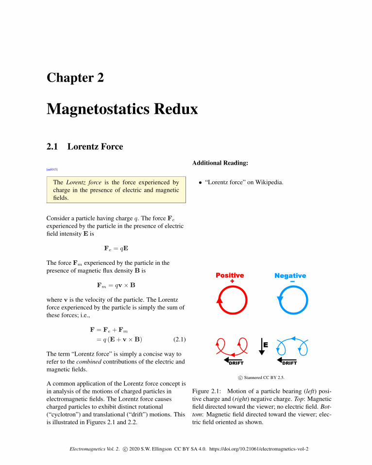
is illustrated in Figures 2.1 and 2.2.
Additional Reading:
• “Lorentz force” on Wikipedia.
c© Stannered CC BY 2.5.
Figure 2.1: Motion of a particle bearing (left) posi-
tive charge and (right) negative charge. Top: Magnetic
field directed toward the viewer; no electric field. Bot-
tom: Magnetic field directed toward the viewer; elec-
tric field oriented as shown.
Electromagnetics Vol. 2. c© 2020 S.W. Ellingson CC BY SA 4.0. https://doi.org/10.21061/electromagnetics-vol-2

12 CHAPTER 2. MAGNETOSTATICS REDUX
c© M. Biaek CC BY-SA 4.0.
Figure 2.2: Electrons moving in a circle in a magnetic
field (cyclotron motion). The electrons are produced
by an electron gun at bottom, consisting of a hot cath-
ode, a metal plate heated by a filament so it emits elec-
trons, and a metal anode at a high voltage with a hole
which accelerates the electrons into a beam. The elec-
trons are normally invisible, but enough air has been
left in the tube so that the air molecules glow pink
when struck by the fast-moving electrons.
2.2 Magnetic Force on a
Current-Carrying Wire
[m0017]
Consider an infinitesimally-thin and
perfectly-conducting wire bearing a current I (SI base
units of A) in free space. Let B (r) be the impressed
magnetic flux density at each point r in the region of
space occupied by the wire. By impressed, we mean
that the field exists in the absence of the
current-carrying wire, as opposed to the field that is
induced by this current. Since current consists of
charged particles in motion, we expect that B(r) will
exert a force on the current. Since the current is
constrained to flow on the wire, we expect this force
will also be experienced by the wire. Let us now
consider this force.
To begin, recall that the force exerted on a particle
bearing charge q having velocity v is
Fm (r) = qv (r)×B (r) (2.2)
Thus, the force exerted on a differential amount of
charge dq is
dFm (r) = dq v (r)×B (r) (2.3)
Let dl (r) represent a differential-length segment of
the wire at r, pointing in the direction of current flow.
Then
dq v (r) = Idl (r) (2.4)
(If this is not clear, it might help to consider the units:
On the left, C·m/s = (C/s)·m = A·m, as on the right.)
Subsequently,
dFm (r) = Idl (r)×B (r) (2.5)
There are three important cases of practical interest.
First, consider a straight segment l forming part of a
closed loop of current in a spatially-uniform
impressed magnetic flux density B (r) = B0. In this
case, the force exerted by the magnetic field on such a
segment is given by Equation 2.5 with dl replaced by
l; i.e.:
Fm = Il×B0 (2.6)
Summarizing,
The force experienced by a straight segment of
current-carrying wire in a spatially-uniform mag-
netic field is given by Equation 2.6.
The second case of practical interest is a rigid closed
loop of current in a spatially-uniform magnetic flux
density B0. If the loop consists of straight sides –
e.g., a rectangular loop – then the force applied to the
loop is the sum of the forces applied to each side
separately, as determined by Equation 2.6. However,
we wish to consider loops of arbitrary shape. To
accommodate arbitrarily-shaped loops, let C be the
path through space occupied by the loop. Then the
force experienced by the loop is
F =
∫
C
dFm (r)
=
∫
C
Idl (r)×B0 (2.7)
Since I and B0 are constants, they may be extracted
from the integral:
F = I
[∫
C
dl (r)
]×B0 (2.8)
Note the quantity in square brackets is zero.
Therefore:

2.2. MAGNETIC FORCE ON A CURRENT-CARRYING WIRE 13
The net force on a current-carrying loop of wire
in a uniform magnetic field is zero.
Note that this does not preclude the possibility that
the rigid loop rotates; for example, the force on
opposite sides of the loop may be equal and opposite.
What we have found is merely that the force will not
lead to a translational net force on the loop; e.g.,
force that would propel the loop away from its current
position in space. The possibility of rotation without
translation leads to the most rudimentary concept for
an electric motor. Practical electric motors use
variations on essentially this same idea; see
“Additional Reading” for more information.
The third case of practical interest is the force
experienced by two parallel infinitesimally-thin wires
in free space, as shown in Figure 2.3. Here the wires
are infinite in length (we’ll return to that in a
moment), lie in the x = 0 plane, are separated by
distance d, and carry currents I1 and I2, respectively.
The current in wire 1 gives rise to a magnetic flux
density B1. The force exerted on wire 2 by B1 is:
F2 =
∫
C
[I2dl (r)×B1 (r)] (2.9)
where C is the path followed by I2, and dl (r) = zdz.
A simple way to determine B1 in this situation is as
follows. First, if wire 1 had been aligned along the
x = y = 0 line, then the magnetic flux density
everywhere would be
φµ0I12πρ
In the present problem, wire 1 is displaced by d/2 in
the −y direction. Although this would seem to make
the new expression more complicated, note that the
only positions where values of B1 (r) are required are
those corresponding to C; i.e., points on wire 2. For
these points,
B1 (r) = −xµ0I12πd
along C (2.10)
That is, the relevant distance is d (not ρ), and the
direction of B1 (r) for points along C is −x (not φ).
Returning to Equation 2.9, we obtain:
F2 =
∫
C
[I2 zdz ×
(−x
µ0I12πd
)]
= −yµ0I1I22πd
∫
C
dz (2.11)
The remaining integral is simply the length of wire 2
that we wish to consider. Infinitely-long wires will
therefore result in infinite force. This is not a very
interesting or useful result. However, the force per
unit length of wire is finite, and is obtained simply by
dropping the integral in the previous equation. We
obtain:F2
∆l= −y
µ0I1I22πd
(2.12)
where ∆l is the length of the section of wire 2 being
considered. Note that when the currents I1 and I2flow in the same direction (i.e., have the same sign),
the magnetic force exerted by the current on wire 1
pulls wire 2 toward wire 1.
The same process can be used to determine the
magnetic force F1 exerted by the current in wire 1 on
wire 2. The result is
F1
∆l= +y
µ0I1I22πd
(2.13)
c© Y. Zhao CC BY-SA 4.0
Figure 2.3: Parallel current-carrying wires.
14 CHAPTER 2. MAGNETOSTATICS REDUX
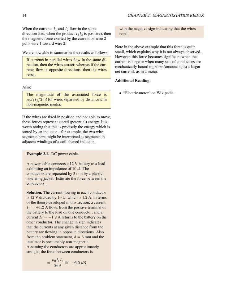
When the currents I1 and I2 flow in the same
direction (i.e., when the product I1I2 is positive), then
the magnetic force exerted by the current on wire 2
pulls wire 1 toward wire 2.
We are now able to summarize the results as follows:
If currents in parallel wires flow in the same di-
rection, then the wires attract; whereas if the cur-
rents flow in opposite directions, then the wires
repel.
Also:
The magnitude of the associated force is
µ0I1I2/2πd for wires separated by distance d in
non-magnetic media.
If the wires are fixed in position and not able to move,
these forces represent stored (potential) energy. It is
worth noting that this is precisely the energy which is
stored by an inductor – for example, the two wire
segments here might be interpreted as segments in
adjacent windings of a coil-shaped inductor.
Example 2.1. DC power cable.
A power cable connects a 12 V battery to a load
exhibiting an impedance of 10 Ω. The
conductors are separated by 3 mm by a plastic
insulating jacket. Estimate the force between the
conductors.
Solution. The current flowing in each conductor
is 12 V divided by 10 Ω, which is 1.2 A. In terms
of the theory developed in this section, a current
I1 = +1.2 A flows from the positive terminal of
the battery to the load on one conductor, and a
current I2 = −1.2 A returns to the battery on the
other conductor. The change in sign indicates
that the currents at any given distance from the
battery are flowing in opposite directions. Also
from the problem statement, d = 3 mm and the
insulator is presumably non-magnetic.
Assuming the conductors are approximately
straight, the force between conductors is
≈ µ0I1I22πd
∼= −96.0 µN
with the negative sign indicating that the wires
repel.
Note in the above example that this force is quite
small, which explains why it is not always observed.
However, this force becomes significant when the
current is large or when many sets of conductors are
mechanically bound together (amounting to a larger
net current), as in a motor.
Additional Reading:
• “Electric motor” on Wikipedia.

2.3. TORQUE INDUCED BY A MAGNETIC FIELD 15
2.3 Torque Induced by a
Magnetic Field
[m0024]
A magnetic field exerts a force on current. This force
is exerted in a direction perpendicular to the direction
of current flow. For this reason, current-carrying
structures in a magnetic field tend to rotate. A
convenient description of force associated with
rotational motion is torque. In this section, we define
torque and apply this concept to a closed loop of
current. These concepts apply to a wide range of
practical devices, including electric motors.
Figure 2.4 illustrates the concept of torque. Torque
depends on the following:
• A local origin r0,
• A point r which is connected to r0 by a
perfectly-rigid mechanical structure, and
• The force F applied at r.
In terms of these parameters, the torque T is:
T , d× F (2.14)
where the lever arm d , r− r0 gives the location of
r relative to r0. Note that T is a position-free vector
c© C. Wang CC BY-SA 4.0
Figure 2.4: Torque associated with a single lever arm.
which points in a direction perpendicular to both d
and F.
Note that T does not point in the direction of rotation.
Nevertheless, T indicates the direction of rotation
through a “right hand rule”: If you point the thumb of
your right hand in the direction of T, then the curled
fingers of your right hand will point in the direction of
torque-induced rotation.
Whether rotation actually occurs depends on the
geometry of the structure. For example, if T aligns
with the axis of a perfectly-rigid mechanical shaft,
then all of the work done by F will be applied to
rotation of the shaft on this axis. Otherwise, torque
will tend to rotate the shaft in other directions as well.
If the shaft is not free to rotate in these other
directions, then the effective torque – that is, the
torque that contributes to rotation of the shaft – is
reduced.
The magnitude of T has SI base units of N·m and
quantifies the energy associated with the rotational
force. As you might expect, the magnitude of the
torque increases with increasing lever arm magnitude
|d|. In other words, the torque resulting from a
constant applied force increases with the length of the
lever arm.
Torque, like the translational force F, satisfies
superposition. That is, the torque resulting from
forces applied to multiple rigidly-connected lever
arms is the sum of the torques applied to the lever
arms individually.
Now consider the current loop shown in Figure 2.5.
The loop is perfectly rigid and is rigidly attached to a
non-conducting shaft. The assembly consisting of the
loop and the shaft may rotate without friction around
the axis of the shaft. The loop consists of four straight
segments that are perfectly-conducting and
infinitesimally-thin. A spatially-uniform and static
impressed magnetic flux density B0 = xB0 exists
throughout the domain of the problem. (Recall that an
impressed field is one that exists in the absence of any
other structure in the problem.) What motion, if any,
is expected?
Recall that the net translational force on a current
loop in a spatially-uniform and static magnetic field is
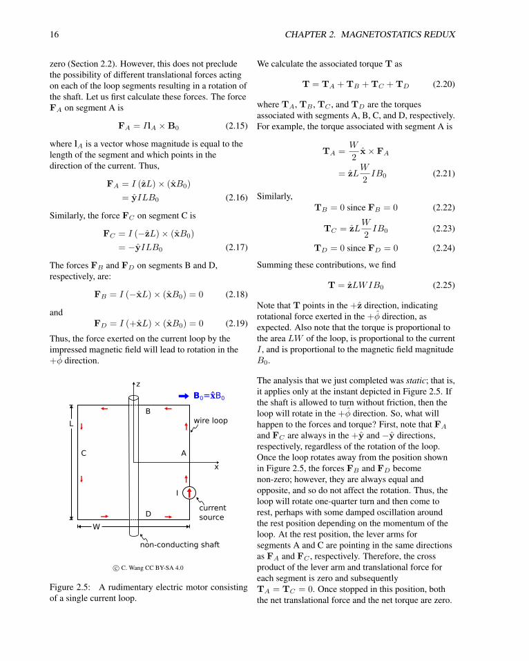
16 CHAPTER 2. MAGNETOSTATICS REDUX
zero (Section 2.2). However, this does not preclude
the possibility of different translational forces acting
on each of the loop segments resulting in a rotation of
the shaft. Let us first calculate these forces. The force
FA on segment A is
FA = IlA ×B0 (2.15)
where lA is a vector whose magnitude is equal to the
length of the segment and which points in the
direction of the current. Thus,
FA = I (zL)× (xB0)
= yILB0 (2.16)
Similarly, the force FC on segment C is
FC = I (−zL)× (xB0)
= −yILB0 (2.17)
The forces FB and FD on segments B and D,
respectively, are:
FB = I (−xL)× (xB0) = 0 (2.18)
and
FD = I (+xL)× (xB0) = 0 (2.19)
Thus, the force exerted on the current loop by the
impressed magnetic field will lead to rotation in the
+φ direction.
z
x
A
B
C
D
L
W
I
B0=xB0
current
source
wire loop
non-conducting shaft
c© C. Wang CC BY-SA 4.0
Figure 2.5: A rudimentary electric motor consisting
of a single current loop.
We calculate the associated torque T as
T = TA +TB +TC +TD (2.20)
where TA, TB , TC , and TD are the torques
associated with segments A, B, C, and D, respectively.
For example, the torque associated with segment A is
TA =W
2x× FA
= zLW
2IB0 (2.21)
Similarly,
TB = 0 since FB = 0 (2.22)
TC = zLW
2IB0 (2.23)
TD = 0 since FD = 0 (2.24)
Summing these contributions, we find
T = zLWIB0 (2.25)
Note that T points in the +z direction, indicating
rotational force exerted in the +φ direction, as
expected. Also note that the torque is proportional to
the area LW of the loop, is proportional to the current
I , and is proportional to the magnetic field magnitude
B0.
The analysis that we just completed was static; that is,
it applies only at the instant depicted in Figure 2.5. If
the shaft is allowed to turn without friction, then the
loop will rotate in the +φ direction. So, what will
happen to the forces and torque? First, note that FAand FC are always in the +y and −y directions,
respectively, regardless of the rotation of the loop.
Once the loop rotates away from the position shown
in Figure 2.5, the forces FB and FD become
non-zero; however, they are always equal and
opposite, and so do not affect the rotation. Thus, the
loop will rotate one-quarter turn and then come to
rest, perhaps with some damped oscillation around
the rest position depending on the momentum of the
loop. At the rest position, the lever arms for
segments A and C are pointing in the same directions
as FA and FC , respectively. Therefore, the cross
product of the lever arm and translational force for
each segment is zero and subsequently
TA = TC = 0. Once stopped in this position, both
the net translational force and the net torque are zero.

2.3. TORQUE INDUCED BY A MAGNETIC FIELD 17
c© Abnormaal CC BY-SA 3.0
Figure 2.6: This DC electric motor uses brushes (here,
the motionless leads labeled “+” and “−”) combined
with the motion of the shaft to periodically alternate
the direction of current between two coils, thereby cre-
ating nearly constant torque.
If such a device is to be used as a motor, it is
necessary to find a way to sustain the rotation. There
are several ways in which this might be accomplished.
First, one might make I variable in time. For
example, the direction of I could be reversed as the
loop passes the quarter-turn position. This reverses
FA and FC , propelling the loop toward the half-turn
position. The direction of I can be changed again as
the loop passes half-turn position, propelling the loop
toward the three-quarter-turn position. Continuing
this periodic reversal of the current sustains the
rotation. Alternatively, one may periodically reverse
the direction of the impressed magnetic field to the
same effect. These methods can be combined or
augmented using multiple current loops or multiple
sets of time-varying impressed magnetic fields. Using
an appropriate combination of current loops,
magnetic fields, and waveforms for each, it is possible
to achieve sustained torque throughout the rotation.
An example is shown in Figure 2.6.
Additional Reading:
• “Torque” on Wikipedia.
• “Electric motor” on Wikipedia.

18 CHAPTER 2. MAGNETOSTATICS REDUX
2.4 The Biot-Savart Law
[m0066]
The Biot-Savart law (BSL) provides a method to
calculate the magnetic field due to any distribution of
steady (DC) current. In magnetostatics, the general
solution to this problem employs Ampere’s law; i.e.,∫
C
H · dl = Iencl (2.26)
in integral form or
∇×H = J (2.27)
in differential form. The integral form is relatively
simple when the problem exhibits a high degree of
symmetry, facilitating a simple description in a
particular coordinate system. An example is the
magnetic field due to a straight and infinitely-long
current filament, which is easily determined by
solving the integral equation in cylindrical
coordinates. However, many problems of practical
interest do not exhibit the necessary symmetry. A
commonly-encountered example is the magnetic field
due to a single loop of current, which will be
addressed in Example 2.2. For such problems, the
differential form of Ampere’s law is needed.
BSL is the solution to the differential form of
Ampere’s law for a differential-length current
element, illustrated in Figure 2.7. The current element
is I dl, where I is the magnitude of the current (SI
base units of A) and dl is a differential-length vector
indicating the direction of the current at the “source
point” r′. The resulting contribution to the magnetic
field intensity at the “field point” r is
dH(r) = I dl1
4πR2× R (2.28)
where
R = RR , r− r′ (2.29)
In other words, R is the vector pointing from the
source point to the field point, and dH at the field
point is given by Equation 2.28. The magnetic field
due to a current-carrying wire of any shape may be
obtained by integrating over the length of the wire:
H(r) =
∫
C
dH(r) =I
4π
∫
C
dl× R
R2(2.30)
In addition to obviating the need to solve a differential
equation, BSL provides some useful insight into the
behavior of magnetic fields. In particular,
Equation 2.28 indicates that magnetic fields follow
the inverse square law – that is, the magnitude of the
magnetic field due to a differential current element
decreases in proportion to the inverse square of
distance (R−2). Also, Equation 2.28 indicates that the
direction of the magnetic field due to a differential
current element is perpendicular to both the direction
of current flow l and the vector R pointing from the
source point to field point. This observation is quite
useful in anticipating the direction of magnetic field
vectors in complex problems.
It may be helpful to note that BSL is analogous to
Coulomb’s law for electric fields, which is a solution
to the differential form of Gauss’ law, ∇ ·D = ρv .
However, BSL applies only under magnetostatic
conditions. If the variation in currents or magnetic
fields over time is significant, then the problem
becomes significantly more complicated. See
“Jefimenko’s Equations” in “Additional Reading” for
more information.
Example 2.2. Magnetic field along the axis of a
circular loop of current.
Consider a ring of radius a in the z = 0 plane,
centered on the origin, as shown in Figure 2.8.
As indicated in the figure, the current I flows in
RR
dH(r)
dl@r'
I
c© C. Wang CC BY-SA 4.0
Figure 2.7: Use of the Biot-Savart law to calculate the
magnetic field due to a line current.

2.4. THE BIOT-SAVART LAW 19
the φ direction. Find the magnetic field intensity
along the z axis.
Solution. The source current position is given in
cylindrical coordinates as
r′ = ρa (2.31)
The position of a field point along the z axis is
r = zz (2.32)
Thus,
RR , r− r′ = −ρa+ zz (2.33)
and
R , |r− r′| =√a2 + z2 (2.34)
Equation 2.28 becomes:
dH(zz) =I φ adφ
4π [a2 + z2]× zz − ρa√
a2 + z2
=Ia
4π
za− ρz
[a2 + z2]3/2
dφ (2.35)
Now integrating over the current:
H(zz) =
∫ 2π
0
Ia
4π
za− ρz
[a2 + z2]3/2
dφ (2.36)
=Ia
4π [a2 + z2]3/2
∫ 2π
0
(za− ρz) dφ
(2.37)
=Ia
4π [a2 + z2]3/2
(za
∫ 2π
0
dφ− z
∫ 2π
0
ρ dφ
)
(2.38)
The second integral is equal to zero. To see this,
note that the integral is simply summing values
of ρ for all possible values of φ. Since
ρ(φ+ π) = −ρ(φ), the integrand for any given
value of φ is equal and opposite the integrand πradians later. (This is one example of a symmetry
argument.)
c© K. Kikkeri CC BY SA 4.0 (modified)
Figure 2.8: Calculation of the magnetic field along
the z axis due to a circular loop of current centered in
the z = 0 plane.
The first integral in the previous equation is
equal to 2π. Thus, we obtain
H(zz) = zIa2
2 [a2 + z2]3/2
(2.39)
Note that the result is consistent with the
associated “right hand rule” of magnetostatics:
That is, the direction of the magnetic field is in
the direction of the curled fingers of the right
hand when the thumb of the right hand is aligned
with the location and direction of current. It is a
good exercise to confirm that this result is also
dimensionally correct.
Equation 2.28 extends straightforwardly to other
distributions of current. For example, the magnetic
field due to surface current Js (SI base units of A/m)
can be calculated using Equation 2.28 with I dlreplaced by
Js ds
where ds is the differential element of surface area.
This can be confirmed by dimensional analysis: I dlhas SI base units of A·m, as does JS ds. Similarly,
the magnetic field due to volume current J (SI base
units of A/m2) can be calculated using Equation 2.28
with I dl replaced by
J dv
where dv is the differential element of volume. For a
single particle with charge q (SI base units of C) and

20 CHAPTER 2. MAGNETOSTATICS REDUX
velocity v (SI base units of m/s), the relevant quantity
is
qv
since C·m/s = (C/s)·m = A·m. In all of these cases,
Equation 2.28 applies with the appropriate
replacement for I dl.
Note that the quantities qv, I dl, JS ds, and J dv, all
having the same units of A·m, seem to be referring to
the same physical quantity. This physical quantity is
known as current moment. Thus, the “input” to BSL
can be interpreted as current moment, regardless of
whether the current of interest is distributed as a line
current, a surface current, a volumetric current, or
simply as moving charged particles. See “Additional
Reading” at the end of this section for additional
information on the concept of “moment” in classical
physics.
Additional Reading:
• “Biot-Savart Law” on Wikipedia.
• “Jefimenko’s Equations” on Wikipedia.
• “Moment (physics)” on Wikipedia.
2.5 Force, Energy, and Potential
Difference in a Magnetic
Field
[m0059]
The force Fm experienced by a particle at location r
bearing charge q due to a magnetic field is
Fm = qv ×B(r) (2.40)
where v is the velocity (magnitude and direction) of
the particle, and B(r) is the magnetic flux density at
r. Now we must be careful: In this description, the
motion of the particle is not due to Fm. In fact the
cross product in Equation 2.40 clearly indicates that
Fm and v must be in perpendicular directions.
Instead, the reverse is true: i.e., it is the motion of the
particle that is giving rise to the force. The motion
described by v may be due to the presence of an
electric field, or it may simply be that that charge is
contained within a structure that is itself in motion.
Nevertheless, the force Fm has an associated
potential energy. Furthermore, this potential energy
may change as the particle moves. This change in
potential energy may give rise to an electrical
potential difference (i.e., a “voltage”), as we shall
now demonstrate.
The change in potential energy can be quantified
using the concept of work, W . The incremental work
∆W done by moving the particle a short distance ∆l,over which we assume the change in Fm is
negligible, is
∆W ≈ Fm · l∆l (2.41)
where in this case l is the unit vector in the direction
of the motion; i.e., the direction of v. Note that the
purpose of the dot product in Equation 2.41 is to
ensure that only the component of Fm parallel to the
direction of motion is included in the energy tally.
Any component of v which is due to Fm (i.e.,
ultimately due to B) must be perpendicular to Fm, so
∆W for such a contribution must be, from
Equation 2.41, equal to zero. In other words: In the
absence of a mechanical force or an electric field, the
potential energy of a charged particle remains
constant regardless of how it is moved by Fm. This
surprising result may be summarized as follows:

2.5. FORCE, ENERGY, AND POTENTIAL DIFFERENCE IN A MAGNETIC FIELD 21
The magnetic field does no work.
Instead, the change of potential energy associated
with the magnetic field must be completely due to a
change in position resulting from other forces, such as
a mechanical force or the Coulomb force. The
presence of a magnetic field merely increases or
decreases this potential difference once the particle
has moved, and it is this change in the potential
difference that we wish to determine.
We can make the relationship between potential
difference and the magnetic field explicit by
substituting the right side of Equation 2.40 into
Equation 2.41, yielding
∆W ≈ q [v ×B(r)] · l∆l (2.42)
Equation 2.42 gives the work only for a short distance
around r. Now let us try to generalize this result. If
we wish to know the work done over a larger
distance, then we must account for the possibility that
v×B varies along the path taken. To do this, we may
sum contributions from points along the path traced
out by the particle, i.e.,
W ≈N∑
n=1
∆W (rn) (2.43)
where rn are positions defining the path. Substituting
the right side of Equation 2.42, we have
W ≈ q
N∑
n=1
[v ×B(rn)] · l(rn)∆l (2.44)
Taking the limit as ∆l → 0, we obtain
W = q
∫
C
[v ×B(r)] · l(r)dl (2.45)
where C is the path (previously, the sequence of rn’s)
followed by the particle. Now omitting the explicit
dependence on r in the integrand for clarity:
W = q
∫
C
[v ×B] · dl (2.46)
where dl = ldl as usual. Now, we are able to
determine the change in potential energy for a
charged particle moving along any path in space,
given the magnetic field.
At this point, it is convenient to introduce the electric
potential difference V21 between the start point (1)
and end point (2) of C. V21 is defined as the work
done by traversing C, per unit of charge; i.e.,
V21 ,W
q(2.47)
This has units of J/C, which is volts (V). Substituting
Equation 2.46, we obtain:
V21 =
∫
C
[v ×B] · dl (2.48)
Equation 2.48 is electrical potential induced by
charge traversing a magnetic field.
Figure 2.9 shows a simple scenario that illustrates this
concept. Here, a straight perfectly-conducting wire of
length l is parallel to the y axis and moves at speed vin the +z direction through a magnetic field B = xB.
Thus,
v ×B = zv × xB
= yBv (2.49)
Taking endpoints 1 and 2 of the wire to be at y = y0
(2)
(1)
B
v
z
y
x
l
c© C. Wang CC BY 4.0
Figure 2.9: A straight wire moving through a mag-
netic field.

22 CHAPTER 2. MAGNETOSTATICS REDUX
and y = y0 + l, respectively, we obtain
V21 =
∫ y0+l
y0
[yBv] · ydy
= Bvl (2.50)
Thus, we see that endpoint 2 is at an electrical
potential of Bvl greater than that of endpoint 1. This
“voltage” exists even though the wire is
perfectly-conducting, and therefore cannot be
attributed to the electric field. This voltage exists even
though the force required for movement must be the
same on both endpoints, or could even be zero, and
therefore cannot be attributed to mechanical forces.
Instead, this change in potential is due entirely to the
magnetic field.
Because the wire does not form a closed loop, no
current flows in the wire. Therefore, this scenario has
limited application in practice. To accomplish
something useful with this concept we must at least
form a closed loop, so that current may flow. For a
closed loop, Equation 2.48 becomes:
V =
∮
C
[v ×B] · dl (2.51)
Examination of this equation indicates one additional
requirement: v ×B must somehow vary over C. This
is because if v ×B does not vary over C, the result
will be
[v ×B] ·∮
C
dl
which is zero because the integral is zero. The
following example demonstrates a practical
application of this idea.
Example 2.3. Potential induced in a
time-varying loop.
Figure 2.10 shows a modification to the problem
originally considered in Figure 2.9. Now, we
have created a closed loop using
perfectly-conducting and motionless wire to
form three sides of a rectangle, and assigned the
origin to the lower left corner. An
infinitesimally-small gap has been inserted in the
left (z = 0) side of the loop and closed with an
ideal resistor of value R. As before, B = xB(spatially uniform and time invariant) and
vB
zx
y
VT
+
-
R
c© C. Wang CC BY-SA 4.0
Figure 2.10: A time-varying loop created by moving
a “shorting bar” along rails comprising two adjacent
sides of the loop.
v = zv (constant). What is the voltage VTacross the resistor and what is the current in the
loop?
Solution. Since the gap containing the resistor is
infinitesimally small,
VT =
∮
C
[v ×B] · dl (2.52)
where C is the perimeter formed by the loop,
beginning at the “−” terminal of VT and
returning to the “+” terminal of VT . Only the
shorting bar is in motion, so v = 0 for the other
three sides of the loop. Therefore, only the
portion of C traversing the shorting bar
contributes to VT . Thus, we find
VT =
∫ l
y=0
[zv × xB] · ydy = Bvl (2.53)
This potential gives rise to a current Bvl/R,
which flows in the counter-clockwise direction.
Note in the previous example that the magnetic field
has induced VT , not the current. The current is simply
a response to the existence of the potential, regardless
of the source. In other words, the same potential VTwould exist even if the gap was not closed by a
resistor.

2.5. FORCE, ENERGY, AND POTENTIAL DIFFERENCE IN A MAGNETIC FIELD 23
Astute readers will notice that this analysis seems to
have a lot in common with Faraday’s law,
V = − ∂
∂tΦ (2.54)
which says the potential induced in a single closed
loop is proportional to the time rate of change of
magnetic flux Φ, where
Φ =
∫
S
B · ds (2.55)
and where S is the surface through which the flux is
calculated. From this perspective, we see that
Equation 2.51 is simply a special case of Faraday’s
law, pertaining specifically to “motional emf.” Thus,
the preceding example can also be solved by
Faraday’s law, taking S to be the time-varying surface
bounded by C.
[m0182]

24 CHAPTER 2. MAGNETOSTATICS REDUX
Image Credits
Fig. 2.1: c© Stannered, https://en.wikipedia.org/wiki/File:Charged-particle-drifts.svg,
CC BY 2.5 (https://creativecommons.org/licenses/by/2.5/deed.en). Modified by Maschen, author.
Fig. 2.2: c© M. Biaek, https://en.wikipedia.org/wiki/File:Cyclotron motion.jpg,
CC BY-SA 4.0 (https://creativecommons.org/licenses/by-sa/4.0/).
Fig. 2.3: c© YahuiZ (Y. Zhao), https://commons.wikimedia.org/wiki/File:Figure2.3Yahui.svg,
CC BY SA 4.0 (https://creativecommons.org/licenses/by-sa/4.0/). Modified by author.
Fig. 2.4: c© Sevenchw (C. Wang),
https://commons.wikimedia.org/wiki/File:Torque associated with a single lever arm.svg,
CC BY SA 4.0 (https://creativecommons.org/licenses/by-sa/4.0/).
Fig. 2.5: c© Sevenchw (C. Wang), https://commons.wikimedia.org/wiki/File:Rudimentary electric motor.svg,
CC BY SA 4.0 (https://creativecommons.org/licenses/by-sa/4.0/).
Fig. 2.6: c© Abnormaal, https://en.wikipedia.org/wiki/File:Electric motor.gif,
CC BY SA 3.0 (https://creativecommons.org/licenses/by-sa/3.0/).
Fig. 2.7: c© Sevenchw (C. Wang),
https://commons.wikimedia.org/wiki/File:Magnetic field due to a line current.svg,
CC BY SA 4.0 (https://creativecommons.org/licenses/by-sa/4.0/).
Fig. 2.8: c© K. Kikkeri, https://commons.wikimedia.org/wiki/File:M0104 fRing.svg,
CC BY SA 4.0 (https://creativecommons.org/licenses/by-sa/4.0/). Modified by author.
Fig. 2.9: c© Sevenchw (C. Wang),
https://commons.wikimedia.org/wiki/File:Straight wire moving in a magnetic field.svg,
CC BY SA 4.0 (https://creativecommons.org/licenses/by-sa/4.0/).
Fig. 2.10: c© Sevenchw (C. Wang),
https://commons.wikimedia.org/wiki/File:Moving shorting bar of a circuit in mag field.svg,
CC BY SA 4.0 (https://creativecommons.org/licenses/by-sa/4.0/).

Chapter 3
Wave Propagation in General Media
3.1 Poynting’s Theorem
[m0073]
Despite the apparent complexity of electromagnetic
theory, there are in fact merely four ways that
electromagnetic energy can be manipulated.
Electromagnetic energy can be:
• Transferred; i.e., conveyed by transmission lines
or in waves;
• Stored in an electric field (capacitance);
• Stored in a magnetic field (inductance); or
• Dissipated (converted to heat; i.e., resistance).
Poynting’s theorem is an expression of conservation
of energy that elegantly relates these various
possibilities. Once recognized, the theorem has
important applications in the analysis and design of
electromagnetic systems. Some of these emerge from
the derivation of the theorem, as opposed to the
unsurprising result. So, let us now derive the theorem.
We begin with a statement of the theorem. Consider a
volume V that may contain materials and structures in
any combination. This is crudely depicted in
Figure 3.1. Also recall that power is the time rate of
change of energy. Then:
Pnet,in = PE + PM + PΩ (3.1)
where Pnet,in is the net power flow into V , PE is the
power associated with energy storage in electric fields
within V , PM is the power associated with energy
storage in magnetic fields within V , and PΩ is the
power dissipated (converted to heat) in V .
Some preliminary mathematical results. We now
derive two mathematical relationships that will be
useful later. Let E be the electric field intensity (SI
base units of V/m) and let D be the electric flux
density (SI base units of C/m2). We require that the
constituents of V be linear and time-invariant;
therefore, D = ǫE where the permittivity ǫ is
constant with respect to time, but not necessarily with
respect to position. Under these conditions, we find
∂
∂t(E ·D) =
1
ǫ
∂
∂t(D ·D) (3.2)
Note that E and D point in the same direction. Let e
be the unit vector describing this direction. Then,
E = eE and D = eD where E and D are the scalar
c© C. Wang CC BY-SA 4.0
Figure 3.1: Poynting’s theorem describes the fate of
power entering a region V consisting of materials and
structures capable of storing and dissipating energy.
Electromagnetics Vol. 2. c© 2020 S.W. Ellingson CC BY SA 4.0. https://doi.org/10.21061/electromagnetics-vol-2
26 CHAPTER 3. WAVE PROPAGATION IN GENERAL MEDIA
components of E and D, respectively. Subsequently,
1
ǫ
∂
∂t(D ·D) =
1
ǫ
∂
∂tD2
=1
ǫ2D
∂
∂tD
= 2E · ∂∂t
D (3.3)
Summarizing:
∂
∂t(E ·D) = 2E · ∂
∂tD (3.4)
which is the expression we seek. It is worth noting
that the expressions on both sides of the equation
have the same units, namely, those of power.
Using the same reasoning, we find:
∂
∂t(H ·B) = 2H · ∂
∂tB (3.5)
where H is the magnetic field intensity (SI base units
of A/m) and B is the magnetic flux density (SI base
units of T).
Derivation of the theorem. We begin with the
differential form of Ampere’s law:
∇×H = J+∂
∂tD (3.6)
Taking the dot product with E on both sides:
E · (∇×H) = E · J+E · ∂∂t
D (3.7)
Let’s deal with the left side of this equation first. For
this, we will employ a vector identity (Equation B.27,
Appendix B.3). This identity states that for any two
vector fields F and G,
∇ · (F×G) = G · (∇× F)− F · (∇×G) (3.8)
Substituting E for F and H for G and rearranging
terms, we find
E · (∇×H) = H · (∇×E)−∇ · (E×H) (3.9)
Next, we invoke the Maxwell-Faraday equation:
∇×E = − ∂
∂tB (3.10)
Using this equation to replace the factor in the
parentheses in the second term of Equation 3.9, we
obtain:
E · (∇×H) = H ·(− ∂
∂tB
)−∇· (E×H) (3.11)
Substituting this expression for the left side of
Equation 3.7, we have
−H · ∂∂t
B−∇· (E×H) = E ·J+E · ∂∂t
D (3.12)
Next we invoke the identities of Equations 3.4 and 3.5
to replace the first and last terms:
−1
2
∂
∂t(H ·B)−∇ · (E×H)
= E · J+1
2
∂
∂t(E ·D) (3.13)
Now we move the first term to the right-hand side and
integrate both sides over the volume V:
−∫
V
∇ · (E×H) dv
=
∫
V
E · J dv
+
∫
V
1
2
∂
∂t(E ·D) dv
+
∫
V
1
2
∂
∂t(H ·B) dv (3.14)
The left side may be transformed into a surface
integral using the divergence theorem:
∫
V
∇ · (E×H) dv =
∮
S
(E×H) · ds (3.15)
where S is the closed surface that bounds V and ds is
the outward-facing normal to this surface, as
indicated in Figure 3.1. Finally, we exchange the
order of time differentiation and volume integration in
the last two terms:
−∮
S
(E×H) · ds
=
∫
V
E · J dv
+1
2
∂
∂t
∫
V
E ·D dv
+1
2
∂
∂t
∫
V
H ·B dv (3.16)

3.1. POYNTING’S THEOREM 27
Equation 3.16 is Poynting’s theorem. Each of the four
terms has the particular physical interpretation
identified in Equation 3.1, as we will now
demonstrate.
Power dissipated by ohmic loss. The first term of
the right side of Equation 3.16 is
PΩ ,
∫
V
E · J dv (3.17)
Equation 3.17 is Joule’s law. Joule’s law gives the
power dissipated due to finite conductivity of
material. The role of conductivity (σ, SI base units of
S/m) can be made explicit using the relationship
J = σE (Ohm’s law) in Equation 3.17, which yields:
PΩ =
∫
V
E · σE dv =
∫
V
σ |E|2 dv (3.18)
PΩ is due to the conversion of the electric field into
conduction current, and subsequently into heat. This
mechanism is commonly known as ohmic loss or
joule heating. It is worth noting that this expression
has the expected units. For example, in
Equation 3.17, E (SI base units of V/m) times J (SI
base units of A/m2) yields a quantity with units of
W/m3; i.e., power per unit volume, which is power
density. Then integration over volume yields units of
W; hence, power.
Energy storage in electric and magnetic fields. The
second term on the right side of Equation 3.16 is:
PE ,1
2
∂
∂t
∫
V
E ·D dv (3.19)
Recall D = ǫE, where ǫ is the permittivity (SI base
units of F/m) of the material. Thus, we may rewrite
the previous equation as follows:
PE =1
2
∂
∂t
∫
V
E · ǫE dv
=1
2
∂
∂t
∫
V
ǫ |E|2 dv
=∂
∂t
(1
2
∫
V
ǫ |E|2 dv)
(3.20)
The quantity in parentheses is We, the energy stored
in the electric field within V .
The third term on the right side of Equation 3.16 is:
PM ,1
2
∂
∂t
∫
V
H ·B dv (3.21)
Recall B = µH, where µ is the permeability (SI base
units of H/m) of the material. Thus, we may rewrite
the previous equation as follows:
PM =1
2
∂
∂t
∫
V
H · µH dv
=1
2
∂
∂t
∫
V
µ |H|2 dv
=∂
∂t
(1
2
∫
V
µ |H|2 dv)
(3.22)
The quantity in parentheses is Wm, the energy stored
in the magnetic field within V .
Power flux through S . The left side of Equation 3.16
is
Pnet,in , −∮
S
(E×H) · ds (3.23)
The quantity E×H is the Poynting vector, which
quantifies the spatial power density (SI base units of
W/m2) of an electromagnetic wave and the direction
in which it propagates. The reader has likely already
encountered this concept. Regardless, we’ll confirm
this interpretation of the quantity E×H in
Section 3.2. For now, observe that integration of the
Poynting vector over S as indicated in Equation 3.23
yields the total power flowing out of V through S .
The negative sign in Equation 3.23 indicates that the
combined quantity represents power flow in to Vthrough S . Finally, note the use of a single quantity
Pnet,in does not imply that power is entirely
inward-directed or outward-directed. Rather, Pnet,inrepresents the net flux; i.e., the sum of the inward-
and outward-flowing power.
Summary. Equation 3.16 may now be stated
concisely as follows:
Pnet,in = PΩ +∂
∂tWe +
∂
∂tWm (3.24)
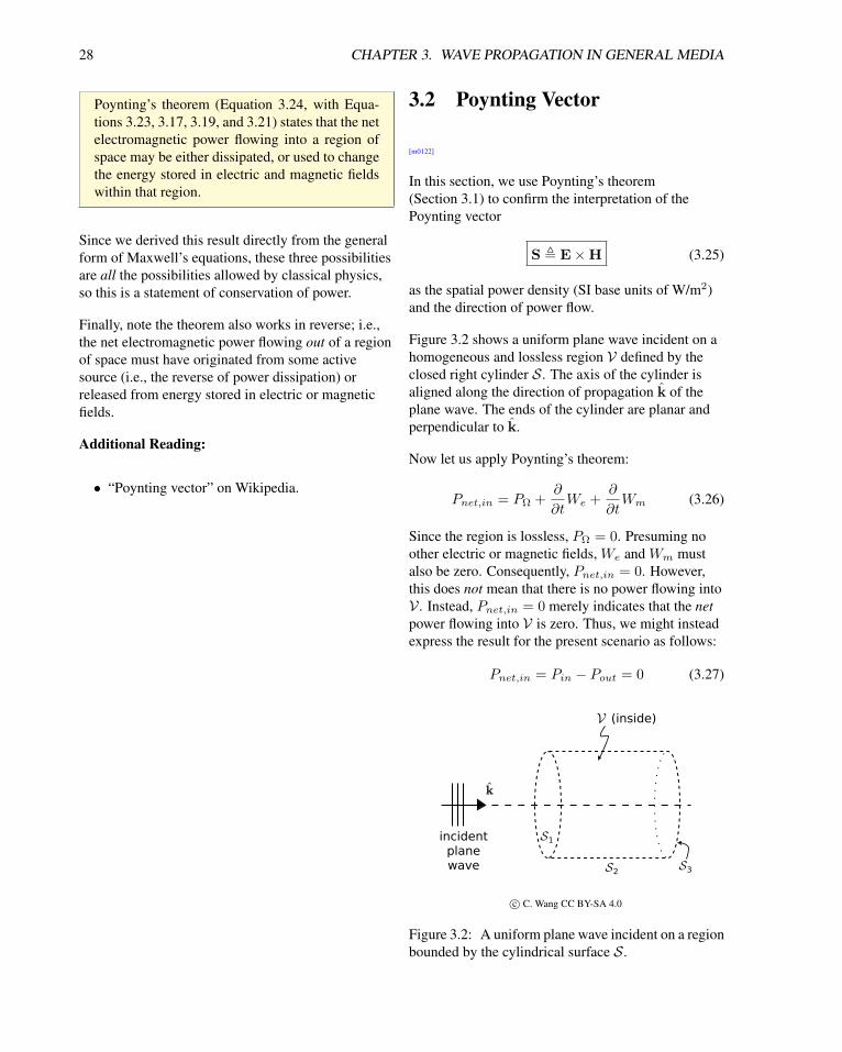
28 CHAPTER 3. WAVE PROPAGATION IN GENERAL MEDIA
Poynting’s theorem (Equation 3.24, with Equa-
tions 3.23, 3.17, 3.19, and 3.21) states that the net
electromagnetic power flowing into a region of
space may be either dissipated, or used to change
the energy stored in electric and magnetic fields
within that region.
Since we derived this result directly from the general
form of Maxwell’s equations, these three possibilities
are all the possibilities allowed by classical physics,
so this is a statement of conservation of power.
Finally, note the theorem also works in reverse; i.e.,
the net electromagnetic power flowing out of a region
of space must have originated from some active
source (i.e., the reverse of power dissipation) or
released from energy stored in electric or magnetic
fields.
Additional Reading:
• “Poynting vector” on Wikipedia.
3.2 Poynting Vector
[m0122]
In this section, we use Poynting’s theorem
(Section 3.1) to confirm the interpretation of the
Poynting vector
S , E×H (3.25)
as the spatial power density (SI base units of W/m2)
and the direction of power flow.
Figure 3.2 shows a uniform plane wave incident on a
homogeneous and lossless region V defined by the
closed right cylinder S . The axis of the cylinder is
aligned along the direction of propagation k of the
plane wave. The ends of the cylinder are planar and
perpendicular to k.
Now let us apply Poynting’s theorem:
Pnet,in = PΩ +∂
∂tWe +
∂
∂tWm (3.26)
Since the region is lossless, PΩ = 0. Presuming no
other electric or magnetic fields, We and Wm must
also be zero. Consequently, Pnet,in = 0. However,
this does not mean that there is no power flowing into
V . Instead, Pnet,in = 0 merely indicates that the net
power flowing into V is zero. Thus, we might instead
express the result for the present scenario as follows:
Pnet,in = Pin − Pout = 0 (3.27)
c© C. Wang CC BY-SA 4.0
Figure 3.2: A uniform plane wave incident on a region
bounded by the cylindrical surface S .
3.2. POYNTING VECTOR 29
where Pin and Pout indicate power flow explicitly
into and explicitly out of V as separate quantities.
Proceeding, let’s ignore what we know about power
flow in plane waves, and instead see where Poynting’s
theorem takes us. Here,
Pnet,in , −∮
S
(E×H) · ds = 0 (3.28)
The surface S consists of three sides: The two flat
ends, and the curved surface that connects them. Let
us refer to these sides as S1, S2, and S3, from left to
right as shown in Figure 3.2. Then,
−∫
S1
(E×H) · ds (3.29)
−∫
S2
(E×H) · ds
−∫
S3
(E×H) · ds = 0
On the curved surface S2, ds is everywhere
perpendicular to E×H (i.e., perpendicular to k).
Therefore, the second integral is equal to zero. On the
left end S1, the outward-facing differential surface
element ds = −kds. On the right end S3,
ds = +kds. We are left with:∫
S1
(E×H) · kds (3.30)
−∫
S3
(E×H) · kds = 0
Compare this to Equation 3.27. Since k is, by
definition, the direction in which E×H points, the
first integral must be Pin and the second integral must
be Pout. Thus,
Pin =
∫
S1
(E×H) · kds (3.31)
and it follows that the magnitude and direction of
E×H, which we recognize as the Poynting vector,
are spatial power density and direction of power flow,
respectively.
The Poynting vector is named after English physicist
J.H. Poynting, one of the co-discoverers of the
concept. The fact that this vector points in the
direction of power flow, and is therefore also a
“pointing vector,” is simply a remarkable coincidence.
Additional Reading:
• “Poynting vector” on Wikipedia.

30 CHAPTER 3. WAVE PROPAGATION IN GENERAL MEDIA
3.3 Wave Equations for Lossy
Regions
[m0128]
The wave equations for electromagnetic propagation
in lossless and source-free media, in differential
phasor form, are:
∇2E+ ω2µǫE = 0 (3.32)
∇2H+ ω2µǫH = 0 (3.33)
The constant ω2µǫ is labeled β2, and β turns out to be
the phase propagation constant.
Now, we wish to upgrade these equations to account
for the possibility of loss. First, let’s be clear on what
we mean by “loss.” Specifically, we mean the
possibility of conversion of energy from the
propagating wave into current, and subsequently to
heat. This mechanism is described by Ohm’s law:
J = σE (3.34)
where σ is conductivity and J is conduction current
density (SI base units of A/m2). In the lossless case, σis presumed to be zero (or at least negligible), so J is
presumed to be zero. To obtain wave equations for
media exhibiting significant loss, we cannot assume
J = 0.
To obtain equations that account for the possibility of
significant conduction current, hence loss, we return
to the phasor forms of Maxwell’s equations:
∇ · E =ρvǫ
(3.35)
∇× E = −jωµH (3.36)
∇ · H = 0 (3.37)
∇× H = J+ jωǫE (3.38)
where ρv is the charge density. If the region of
interest is source-free, then ρv = 0. However, we may
not similarly suppress J since σ may be non-zero. To
make progress, let us identify the possible
contributions to J as follows:
J = Jimp + Jind (3.39)
where Jimp represents impressed sources of current
and Jind represents current which is induced by loss.
An impressed current is one whose behavior is
independent of other features, analogous to an
independent current source in elementary circuit
theory. In the absence of such sources, Equation 3.39
becomes:
J = 0 + σE (3.40)
Equation 3.38 may now be rewritten as:
∇× H = σE+ jωǫE (3.41)
= (σ + jωǫ) E (3.42)
= jωǫcE (3.43)
where we defined the new constant ǫc as follows:
ǫc , ǫ− jσ
ω(3.44)
This constant is known as complex permittivity. In
the lossless case, ǫc = ǫ; i.e., the imaginary part of
ǫc → 0 so there is no difference between the physical
permittivity ǫ and ǫc. The effect of the material’s loss
is represented as a non-zero imaginary component of
the permittivity.
It is also common to express ǫc as follows:
ǫc = ǫ′ − jǫ′′ (3.45)
where the real-valued constants ǫ′ and ǫ′′ are in this
case:
ǫ′ = ǫ (3.46)
ǫ′′ =σ
ω(3.47)
This alternative notation is useful for three reasons.
First, some authors use the symbol ǫ to refer to both
physical permittivity and complex permittivity. In this
case, the “ǫ′ − jǫ′′” notation is helpful in mitigating
confusion. Second, it is often more convenient to
specify ǫ′′ at a frequency than it is to specify σ, which
may also be a function of frequency. In fact, in some
applications the loss of a material is most
conveniently specified using the ratio ǫ′′/ǫ′ (known as
loss tangent, for reasons explained elsewhere).
Finally, it turns out that nonlinearity of permittivity
can also be accommodated as an imaginary

3.3. WAVE EQUATIONS FOR LOSSY REGIONS 31
component of the permittivity. The “ǫ′′” notation
allows us to accommodate both effects – nonlinearity
and conductivity – using common notation. In this
section, however, we remain focused exclusively on
conductivity.
Complex permittivity ǫc (SI base units of F/m)
describes the combined effects of permittivity
and conductivity. Conductivity is represented as
an imaginary-valued component of the permittiv-
ity.
Returning to Equations 3.35–3.38, we obtain:
∇ · E = 0 (3.48)
∇× E = −jωµH (3.49)
∇ · H = 0 (3.50)
∇× H = jωǫcE (3.51)
These equations are identical to the corresponding
equations for the lossless case, with the exception that
ǫ has been replaced by ǫc. Similarly, we may replace
the factor ω2µǫ in Equations 3.32 and 3.33, yielding:
∇2E+ ω2µǫcE = 0 (3.52)
∇2H+ ω2µǫcH = 0 (3.53)
In the lossless case, ω2µǫc → ω2µǫ, which is β2 as
expected. For the general (i.e., possibly lossy) case,
we shall make an analogous definition
γ2 , −ω2µǫc (3.54)
such that the wave equations may now be written as
follows:
∇2E− γ2E = 0 (3.55)
∇2H− γ2H = 0 (3.56)
Note the minus sign in Equation 3.54, and the
associated changes of signs in Equations 3.55 and
3.56. For the moment, this choice of sign may be
viewed as arbitrary – we would have been equally
justified in choosing the opposite sign for the
definition of γ2. However, the choice we have made
is customary, and yields some notational convenience
that will become apparent later.
In the lossless case, β is the phase propagation
constant, which determines the rate at which the
phase of a wave progresses with increasing distance
along the direction of propagation. Given the
similarity of Equations 3.55 and 3.56 to
Equations 3.32 and 3.33, respectively, the constant γmust play a similar role. So, we are motivated to find
an expression for γ. At first glance, this is simple:
γ =√γ2. However, recall that every number has two
square roots. When one declares β =√β2 = ω
√µǫ,
there is no concern since β is, by definition, positive;
therefore, one knows to take the positive-valued
square root. In contrast, γ2 is complex-valued, and so
the two possible values of√γ2 are both potentially
complex-valued. We are left without clear guidance
on which of these values is appropriate and
physically-relevant. So we proceed with caution.
First, consider the special case that γ is purely
imaginary; e.g., γ = jγ′′ where γ′′ is a real-valued
constant. In this case, γ2 = − (γ′′)2
and the wave
equations become
∇2E+ (γ′′)2E = 0 (3.57)
∇2H+ (γ′′)2H = 0 (3.58)
Comparing to Equations 3.32 and 3.33, we see γ′′
plays the exact same role as β; i.e., γ′′ is the phase
propagation constant for whatever wave we obtain as
the solution to the above equations. Therefore, let us
make that definition formally:
β , Im γ (3.59)
Be careful: Note that we are not claiming that γ′′ in
the possibly-lossy case is equal to ω2µǫ. Instead, we
are asserting exactly the opposite; i.e., that there is a
phase propagation constant in the general (possibly
lossy) case, and we should find that this constant
simplifies to ω2µǫ in the lossless case.
Now we make the following definition for the real
component of γ:
α , Re γ (3.60)
Such that
γ = α+ jβ (3.61)
where α and β are real-valued constants.
Now, it is possible to determine γ explicitly in terms
of ω and the constitutive properties of the material.

32 CHAPTER 3. WAVE PROPAGATION IN GENERAL MEDIA
First, note:
γ2 = (α+ jβ)2
= α2 − β2 + j2αβ (3.62)
Expanding Equation 3.54 using Equations 3.45–3.47,
we obtain:
γ2 = −ω2µ(ǫ− j
σ
ω
)
= −ω2µǫ+ jωµσ (3.63)
The real and imaginary parts of Equations 3.62 and
3.63 must be equal. Enforcing this equality yields the
following equations:
α2 − β2 = −ω2µǫ (3.64)
2αβ = ωµσ (3.65)
Equations 3.64 and 3.65 are independent
simultaneous equations that may be solved for α and
β. Sparing the reader the remaining steps, which are
purely mathematical, we find:
α = ω
µǫ′
2
√
1 +
(ǫ′′
ǫ′
)2
− 1
1/2
(3.66)
β = ω
µǫ′
2
√
1 +
(ǫ′′
ǫ′
)2
+ 1
1/2
(3.67)
Equations 3.66 and 3.67 can be verified by confirming
that Equations 3.64 and 3.65 are satisfied. It is also
useful to confirm that the expected results are
obtained in the lossless case. In the lossless case,
σ = 0, so ǫ′′ = 0. Subsequently, Equation 3.66 yields
α = 0 and Equation 3.67 yields β = ω√µǫ, as
expected.
The electromagnetic wave equations account-
ing for the possibility of lossy media are Equa-
tions 3.55 and 3.56 with γ = α + jβ, where αand β are the positive real-valued constants deter-
mined by Equations 3.66 and 3.67, respectively.
We conclude this section by pointing out a very useful
analogy to transmission line theory. In the section
“Wave Propagation on a TEM Transmission Line,”1
we found that the potential and current along a
transverse electromagnetic (TEM) transmission line
satisfy the same wave equations that we have
developed in this section, having a complex-valued
propagation constant γ = α+ jβ, and the same
physical interpretation of β as the phase propagation
constant. As is explained in another section, α too has
the same interpretation in both applications – that is,
as the attenuation constant.
Additional Reading:
• “Electromagnetic Wave Equation” on Wikipedia.
1This section may appear in a different volume, depending on
the version of this book.
3.4. COMPLEX PERMITTIVITY 33
3.4 Complex Permittivity
[m0134]
The relationship between electric field intensity E (SI
base units of V/m) and electric flux density D (SI
base units of C/m2) is:
D = ǫE (3.68)
where ǫ is the permittivity (SI base units of F/m). In
simple media, ǫ is a real positive value which does not
depend on the time variation of E. That is, the
response (D) to a change in E is observed
instantaneously and without delay.
In practical materials, however, the change in D in
response to a change in E may depend on the manner
in which E changes. The response may not be
instantaneous, but rather might take some time to
fully manifest. This behavior can be modeled using
the following generalization of Equation 3.68:
D = a0E+a1∂
∂tE+a2
∂2
∂t2E+a3
∂3
∂t3E+ ... (3.69)
where a0, a1, a2, and so on are real-valued constants,
and the number of terms is infinite. In practical
materials, the importance of the terms tends to
diminish with increasing order. Thus, it is common
that only the first few terms are significant. In many
applications involving common materials, only the
first term is significant; i.e., a0 ≈ ǫ and an ≈ 0 for
n ≥ 1. As we shall see in a moment, this distinction
commonly depends on frequency.
In the phasor domain, differentiation with respect to
time becomes multiplication by jω. Thus,
Equation 3.69 becomes
D = a0E+ a1 (jω) E+ a2 (jω)2E+ a3 (jω)
3E+ ...
= a0E+ jωa1E− ω2a2E− jω3a3E+ ...
=(a0 + jωa1 − ω2a2 − jω3a3 + ...
)E (3.70)
Note that the factor in parentheses is a
complex-valued number which depends on frequency
ω and materials parameters a0, a1, ... We may
summarize this as follows:
D = ǫcE (3.71)
where ǫc is a complex-valued constant that depends
on frequency.
The notation “ǫc” is used elsewhere in this book (e.g.,
Section 3.3) to represent a generalization of simple
permittivity that accommodates loss associated with
non-zero conductivity σ. In Section 3.3, we defined
ǫc , ǫ′ − jǫ′′ (3.72)
where ǫ′ , ǫ (i.e., real-valued, simple permittivity)
and ǫ′′ , σ/ω (i.e., the effect of non-zero
conductivity). Similarly, ǫc in Equation 3.71 can be
expressed as
ǫc , ǫ′ − jǫ′′ (3.73)
but in this case
ǫ′ , a0 − ω2a2 + ... (3.74)
and
ǫ′′ , −ωa1 + ω3a3 − ... (3.75)
When expressed as phasors, the temporal rela-
tionship between electric flux density and elec-
tric field intensity can be expressed as a complex-
valued permittivity.
Thus, we now see two possible applications for the
concept of complex permittivity: Modeling the
delayed response of D to changing E, as described
above; and modeling loss associated with non-zero
conductivity. In practical work, it may not always be
clear precisely what combination of effects the
complex permittivity ǫc = ǫ′ − jǫ′′ is taking into
account. For example, if ǫc is obtained by
measurement, both delayed response and conduction
loss may be represented. Therefore, it is not
reasonable to assume a value of ǫ′′ obtained by
measurement represents only conduction loss (i.e., is
equal to σ/ω); in fact, the measurement also may
include a significant frequency-dependent
contribution associated with the delayed response
behavior identified in this section.
An example of the complex permittivity of a typical
dielectric material is shown in Figure 3.3. Note the
frequency dependence is quite simple and
slowly-varying at frequencies below 1 GHz or so, but
becomes relatively complex at higher frequencies.

34 CHAPTER 3. WAVE PROPAGATION IN GENERAL MEDIA
c© K.A. Mauritz (modified)
Figure 3.3: The relative contributions of the real and
imaginary components of permittivity for a typical di-
electric material (in this case, a polymer).
Additional Reading:
• “Permittivity” on Wikipedia.
3.5 Loss Tangent
[m0132]
In Section 3.3, we found that the effect of loss due to
non-zero conductivity σ could be concisely quantified
using the ratioǫ′′
ǫ′=
σ
ωǫ(3.76)
where ǫ′ and ǫ′′ are the real and imaginary
components of the complex permittivity ǫc, and
ǫ′ , ǫ. In this section, we explore this relationship in
greater detail.
Recall Ampere’s law in differential (but otherwise
general) form:
∇×H = J+∂
∂tD (3.77)
The first term on the right is conduction current,
whereas the second term on the right is displacement
current. In the phasor domain, differentiation with
respect to time (∂/∂t) becomes multiplication by jω.
Therefore, the phasor form of Equation 3.77 is
∇× H = J+ jωD (3.78)
Also recall that J = σE and that D = ǫE. Thus,
∇× H = σE+ jωǫE (3.79)
Interestingly, the total current is the sum of a
real-valued conduction current and an
imaginary-valued displacement current. This is
shown graphically in Figure 3.4.
Note that the angle δ indicated in Figure 3.4 is given
by
tan δ ,σ
ωǫ(3.80)
The quantity tan δ is referred to as the loss tangent.
Note that loss tangent is zero for a lossless (σ ≡ 0)
material, and increases with increasing loss. Thus,
loss tangent provides an alternative way to quantify
the effect of loss on the electromagnetic field within a
material.
Loss tangent presuming only ohmic (conduction)
loss is given by Equation 3.80.

3.5. LOSS TANGENT 35
Comparing Equation 3.80 to Equation 3.76, we see
loss tangent can equivalently be calculated as
tan δ =ǫ′′
ǫ(3.81)
and subsequently interpreted as shown in Figure 3.5.
The discussion in this section has assumed that ǫc is
complex-valued solely due to ohmic loss. However, it
is explained in Section 3.4 that permittivity may also
be complex-valued as a way to model delay in the
response of D to changing E. Does the concept of
loss tangent apply also in this case? Since the math
does not distinguish between permittivity which is
complex due to loss and permittivity which is
complex due to delay, subsequent
mathematically-derived results apply in either case.
On the other hand, there may be potentially
significant differences in the physical manifestation of
these effects. For example, a material having large
loss tangent due to ohmic loss might become hot
when a large electric field is applied, whereas a
material having large loss tangent due to delayed
response might not. Summarizing:
The expression for loss tangent given by Equa-
tion 3.81 and Figure 3.5 does not distinguish be-
tween ohmic loss and delayed response.
c© C. Wang CC BY-SA 4.0
Figure 3.4: In the phasor domain, the total current
is the sum of a real-valued conduction current and an
imaginary-valued displacement current.
c© C. Wang CC BY-SA 4.0
Figure 3.5: Loss tangent defined in terms of the real
and imaginary components of the complex permittiv-
ity ǫc.
Additional Reading:
• “Dielectric loss” on Wikipedia.

36 CHAPTER 3. WAVE PROPAGATION IN GENERAL MEDIA
3.6 Plane Waves in Lossy Regions
[m0130]
The electromagnetic wave equations for source-free
regions consisting of possibly-lossy material are (see
Section 3.3):
∇2E− γ2E = 0 (3.82)
∇2H− γ2H = 0 (3.83)
where
γ2 , −ω2µǫc (3.84)
We now turn our attention to the question, what are
the characteristics of waves that propagate in these
conditions? As in the lossless case, these equations
permit waves having a variety of geometries including
plane waves, cylindrical waves, and spherical waves.
In this section, we will consider the important special
case of uniform plane waves.
To obtain the general expression for the uniform
plane wave solution, we follow precisely the same
procedure described in the section “Uniform Plane
Waves: Derivation.”2 Although that section presumed
lossless media, the only difference in the present
situation is that the real-valued constant +β2 is
replaced with the complex-valued constant −γ2.
Thus, we obtain the desired solution through a simple
modification of the solution for the lossless case. For
a wave exhibiting uniform magnitude and phase in
planes of constant z, we find that the electric field is:
E = xEx + yEy (3.85)
where
Ex = E+x0e
−γz + E−x0e
+γz (3.86)
Ey = E+y0e
−γz + E−y0e
+γz (3.87)
where the complex-valued coefficients E+x0, E−
x0,
E+y0, and E−
y0 are determined by boundary conditions
(possibly including sources) outside the region of
interest. This result can be confirmed by verifying
that Equations 3.86 and 3.87 each satisfy
Equation 3.82. Also, it may be helpful to note that
these expressions are identical to those obtained for
2Depending on the version of this book, this section may appear
in a different volume.
the voltage and current in lossy transmission lines, as
described in the section “Wave Equation for a TEM
Transmission Line.”3
Let’s consider the special case of an x-polarized plane
wave propagating in the +z direction:
E = xE+x0e
−γz (3.88)
We established in Section 3.3 that γ may be written
explicitly in terms of its real and imaginary
components as follows:
γ = α+ jβ (3.89)
where α and β are positive real-valued constants
depending on frequency (ω) and constitutive
properties of the medium; i.e., permittivity,
permeability, and conductivity. Thus:
E = xE+x0e
−(α+jβ)z
= xE+x0e
−αze−jβz (3.90)
Observe that the variation of phase with distance is
determined by β through the factor e−jβz; thus, β is
the phase propagation constant and plays precisely
the same role as in the lossless case. Observe also that
the variation in magnitude is determined by α through
the real-valued factor e−αz . Specifically, magnitude is
reduced inverse-exponentially with increasing
distance along the direction of propagation. Thus, αis the attenuation constant and plays precisely the
same role as the attenuation constant for a lossy
transmission line.
The presence of loss in material gives rise to a
real-valued factor e−αz which describes the at-
tenuation of the wave with propagation (in this
case, along z) in the material.
We may continue to exploit the similarity of the
potentially-lossy and lossless plane wave results to
quickly ascertain the characteristics of the magnetic
field. In particular, the plane wave relationships apply
exactly as they do in the lossless case. These
relationships are:
H =1
ηk× E (3.91)
3Depending on the version of this book, this section may appear
in a different volume.

3.7. WAVE POWER IN A LOSSY MEDIUM 37
E = −ηk× H (3.92)
where k is the direction of propagation and η is the
wave impedance. In the lossless case, η =√µ/ǫ;
however, in the possibly-lossy case we must replace
ǫ = ǫ′ with ǫc = ǫ′ − jǫ′′. Thus:
η → ηc =
õ
ǫc=
õ
ǫ′ − jǫ′′
=
õ
ǫ′
√1
1− j (ǫ′′/ǫ′)(3.93)
Thus:
ηc =
õ
ǫ′·[1− j
ǫ′′
ǫ′
]−1/2
(3.94)
Remarkably, we find that the wave impedance for a
lossy material is equal to√µ/ǫ – the wave
impedance we would calculate if we neglected loss
(i.e., assumed σ = 0) – times a correction factor that
accounts for the loss. This correction factor is
complex-valued; therefore, E and H are not in phase
when propagating through lossy material. We now
see that in the phasor domain:
H =1
ηck× E (3.95)
E = −ηck× H (3.96)
The plane wave relationships in media which are
possibly lossy are given by Equations 3.95 and
3.96, with the complex-valued wave impedance
given by Equation 3.94.
3.7 Wave Power in a Lossy
Medium
[m0133]
In this section, we consider the power associated with
waves propagating in materials which are potentially
lossy; i.e., having conductivity σ significantly greater
than zero. This topic has previously been considered
in the section “Wave Power in a Lossless Medium”
for the case in loss is not significant.4 A review of that
section may be useful before reading this section.
Recall that the Poynting vector
S , E×H (3.97)
indicates the power density (i.e., W/m2) of a wave and
the direction of power flow. This is “instantaneous”
power, applicable to waves regardless of the way they
vary with time. Often we are interested specifically in
waves which vary sinusoidally, and which
subsequently may be represented as phasors. In this
case, the time-average Poynting vector is
Save ,1
2ReE× H∗
(3.98)
Further, we have already used this expression to find
that the time-average power density for a
sinusoidally-varying uniform plane wave in a lossless
medium is simply
Save =|E0|22η
(lossless case) (3.99)
where |E0| is the peak (as opposed to RMS)
magnitude of the electric field intensity phasor, and ηis the wave impedance.
Let us now use Equation 3.98 to determine the
expression corresponding to Equation 3.99 in the case
of possibly-lossy media. We may express the electric
and magnetic field intensities of a uniform plane wave
as
E = xE0e−αze−jβz (3.100)
and
H = yE0
ηce−αze−jβz (3.101)
4Depending on the version of this book, this section may appear
in another volume.

38 CHAPTER 3. WAVE PROPAGATION IN GENERAL MEDIA
where α and β are the attenuation constant and phase
propagation constant, respectively, and ηc is the
complex-valued wave impedance. As written, these
expressions describe a wave which is +x-polarized
and propagates in the +z direction. We make these
choices for convenience only – as long as the medium
is homogeneous and isotropic, we expect our findings
to apply regardless of polarization and direction of
propagation. Applying Equation 3.98:
Save =1
2ReE× H∗
=1
2z Re
|E0|2η∗c
e−2αz
= z|E0|22
Re
1
η∗c
e−2αz (3.102)
Because ηc is complex-valued when the material is
lossy, we must proceed with caution. First, let us
write ηc explicitly in terms of its magnitude |ηc| and
phase ψη:
η , |η| ejψη (3.103)
Then:
η∗c = |ηc| e−jψη (3.104)
(η∗c )−1
= |ηc|−1e+jψη (3.105)
Re(η∗c )
−1= |ηc|−1
cosψη (3.106)
Then Equation 3.102 may be written:
Save = z|E0|22 |ηc|
e−2αz cosψη (3.107)
The time-average power density of the plane
wave described by Equation 3.100 in a possibly-
lossy material is given by Equation 3.107.
As a check, note that this expression gives the
expected result for lossless media; i.e., α = 0,
|ηc| = η, and ψη = 0. We now see that the effect of
loss is that power density is now proportional to
(e−αz)2, so, as expected, power density is
proportional to the square of either |E| or |H|. The
result further indicates a one-time scaling of the
power density by a factor of
|η||ηc|
cosψη < 1 (3.108)
relative to a medium without loss.
The reduction in power density due to non-
zero conductivity is proportional to a distance-
dependent factor e−2αz and an additional factor
that depends on the magnitude and phase of ηc.
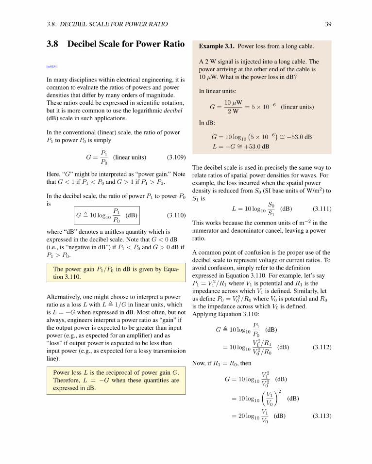
3.8. DECIBEL SCALE FOR POWER RATIO 39
3.8 Decibel Scale for Power Ratio
[m0154]
In many disciplines within electrical engineering, it is
common to evaluate the ratios of powers and power
densities that differ by many orders of magnitude.
These ratios could be expressed in scientific notation,
but it is more common to use the logarithmic decibel
(dB) scale in such applications.
In the conventional (linear) scale, the ratio of power
P1 to power P0 is simply
G =P1
P0(linear units) (3.109)
Here, “G” might be interpreted as “power gain.” Note
that G < 1 if P1 < P0 and G > 1 if P1 > P0.
In the decibel scale, the ratio of power P1 to power P0
is
G , 10 log10P1
P0(dB) (3.110)
where “dB” denotes a unitless quantity which is
expressed in the decibel scale. Note that G < 0 dB
(i.e., is “negative in dB”) if P1 < P0 and G > 0 dB if
P1 > P0.
The power gain P1/P0 in dB is given by Equa-
tion 3.110.
Alternatively, one might choose to interpret a power
ratio as a loss L with L , 1/G in linear units, which
is L = −G when expressed in dB. Most often, but not
always, engineers interpret a power ratio as “gain” if
the output power is expected to be greater than input
power (e.g., as expected for an amplifier) and as
“loss” if output power is expected to be less than
input power (e.g., as expected for a lossy transmission
line).
Power loss L is the reciprocal of power gain G.
Therefore, L = −G when these quantities are
expressed in dB.
Example 3.1. Power loss from a long cable.
A 2 W signal is injected into a long cable. The
power arriving at the other end of the cable is
10 µW. What is the power loss in dB?
In linear units:
G =10 µW
2 W= 5× 10⁻⁶ (linear units)
In dB:
G = 10 log10(5× 10⁻⁶
) ∼= −53.0 dB
L = −G ∼= +53.0 dB
The decibel scale is used in precisely the same way to
relate ratios of spatial power densities for waves. For
example, the loss incurred when the spatial power
density is reduced from S0 (SI base units of W/m2) to
S1 is
L = 10 log10S0
S1(dB) (3.111)
This works because the common units of m−2 in the
numerator and denominator cancel, leaving a power
ratio.
A common point of confusion is the proper use of the
decibel scale to represent voltage or current ratios. To
avoid confusion, simply refer to the definition
expressed in Equation 3.110. For example, let’s say
P1 = V 21 /R1 where V1 is potential and R1 is the
impedance across which V1 is defined. Similarly, let
us define P0 = V 20 /R0 where V0 is potential and R0
is the impedance across which V0 is defined.
Applying Equation 3.110:
G , 10 log10P1
P0(dB)
= 10 log10V 21 /R1
V 20 /R0
(dB) (3.112)
Now, if R1 = R0, then
G = 10 log10V 21
V 20
(dB)
= 10 log10
(V1V0
)2
(dB)
= 20 log10V1V0
(dB) (3.113)

40 CHAPTER 3. WAVE PROPAGATION IN GENERAL MEDIA
However, note that this is not true if R1 6= R0.
A power ratio in dB is equal to 20 log10 of the
voltage ratio only if the associated impedances
are equal.
Adding to the potential for confusion on this point is
the concept of voltage gain Gv:
Gv , 20 log10V1V0
(dB) (3.114)
which applies regardless of the associated
impedances. Note that Gv = G only if the associated
impedances are equal, and that these ratios are
different otherwise. Be careful!
The decibel scale simplifies common calculations.
Here’s an example. Let’s say a signal having power
P0 is injected into a transmission line having loss L.
Then the output power P1 = P0/L in linear units.
However, in dB, we find:
10 log10 P1 = 10 log10P0
L= 10 log10 P0 − 10 log10 L
Division has been transformed into subtraction; i.e.,
P1 = P0 − L (dB) (3.115)
This form facilitates easier calculation and
visualization, and so is typically preferred.
Finally, note that the units of P1 and P0 in
Equation 3.115 are not dB per se, but rather dB with
respect to the original power units. For example, if P1
is in mW, then taking 10 log10 of this quantity results
in a quantity having units of dB relative to 1 mW. A
power expressed in dB relative to 1 mW is said to
have units of “dBm.” For example, “0 dBm” means
0 dB relative to 1 mW, which is simply 1 mW.
Similarly +10 dBm is 10 mW, −10 dBm is 0.1 mW,
and so on.
Additional Reading:
• “Decibel” on Wikipedia.
• “Scientific notation” on Wikipedia.
3.9 Attenuation Rate
[m0155]
Attenuation rate is a convenient way to quantify loss
in general media, including transmission lines, using
the decibel scale.
Consider a transmission line carrying a wave in the
+z direction. Let P0 be the power at z = 0. Let P1 be
the power at z = l. Then the power at z = 0 relative
to the power at z = l is:
P0
P1=e−2α·0
e−2α·l= e2αl (linear units) (3.116)
where α is the attenuation constant; that is, the real
part of the propagation constant γ = α+ jβ.
Expressed in this manner, the power ratio is a loss;
that is, a number greater than 1 represents attenuation.
In the decibel scale, the loss is
10 log10P0
P1= 10 log10 e
2αl
= 20αl log10 e∼= 8.69αl dB (3.117)
Attenuation rate is defined as this quantity per unit
length. Dividing by l, we obtain:
attenuation rate ∼= 8.69α (3.118)
This has units of dB/length, where the units of length
are the same length units in which α is expressed. For
example, if α is expressed in units of m−1, then
attenuation rate has units of dB/m.
Attenuation rate ∼= 8.69α is the loss in dB, per
unit length.
The utility of the attenuation rate concept is that it
allows us to quickly calculate loss for any distance of
wave travel: This loss is simply attenuation rate
(dB/m) times length (m), which yields loss in dB.
Example 3.2. Attenuation rate in a long cable.
A particular coaxial cable has an attenuation
constant α ∼= 8.5× 10⁻³ m−1. What is the
attenuation rate and the loss in dB for 100 m of
this cable?

3.10. POOR CONDUCTORS 41
The attenuation rate is
∼= 8.69α ∼= 0.0738 dB/m
The loss in 100 m of this cable is
∼= (0.0738 dB/m) (100 m) ∼= 7.4 dB
Note that it would be entirely appropriate, and
equivalent, to state that the attenuation rate for
this cable is 7.4 dB/(100 m).
The concept of attenuation rate is used in precisely
the same way to relate ratios of spatial power
densities for unguided waves. This works because
spatial power density has SI base units of W/m2, so
the common units of m−2 in the numerator and
denominator cancel in the power density ratio,
leaving a simple power ratio.
3.10 Poor Conductors
[m0156]
A poor conductor is a material for which conductivity
is low, yet sufficient to exhibit significant loss. To be
clear, the loss we refer to here is the conversion of the
electric field to current through Ohm’s law.
The threshold of significance depends on the
application. For example, the dielectric spacer
separating the conductors in a coaxial cable might be
treated as lossless (σ = 0) for short lengths at low
frequencies; whereas the loss of the cable for long
lengths and higher frequencies is typically significant,
and must be taken into account. In the latter case, the
material is said to be a poor conductor because the
loss is significant yet the material can still be treated
in most other respects as an ideal dielectric.
A quantitative but approximate criterion for
identification of a poor conductor can be obtained
from the concept of complex permittivity ǫc, which
has the form:
ǫc = ǫ′ − jǫ′′ (3.119)
Recall that ǫ′′ quantifies loss, whereas ǫ′ exists
independently of loss. In fact, ǫc = ǫ′ = ǫ for a
perfectly lossless material. Therefore, we may
quantify the lossiness of a material using the ratio
ǫ′′/ǫ′, which is sometimes referred to as loss tangent
(see Section 3.5). Using this quantity, we define a
poor conductor as a material for which ǫ′′ is very
small relative to ǫ′. Thus,
ǫ′′
ǫ′≪ 1 (poor conductor) (3.120)
A poor conductor is a material having loss tan-
gent much less than 1, such that it behaves in
most respects as an ideal dielectric except that
ohmic loss may not be negligible.
An example of a poor conductor commonly
encountered in electrical engineering includes the
popular printed circuit board substrate material FR4
(fiberglass epoxy), which has ǫ′′/ǫ′ ∼ 0.008 over the
frequency range it is most commonly used. Another
example, already mentioned, is the dielectric spacer
42 CHAPTER 3. WAVE PROPAGATION IN GENERAL MEDIA
material (for example, polyethylene) typically used in
coaxial cables. The loss of these materials may or
may not be significant, depending on the particulars
of the application.
The imprecise definition of Equation 3.120 is
sufficient to derive some characteristics exhibited by
all poor conductors. To do so, first recall that the
propagation constant γ is given in general as follows:
γ2 = −ω2µǫc (3.121)
Therefore:
γ =√
−ω2µǫc (3.122)
In general a number has two square roots, so some
caution is required here. In this case, we may proceed
as follows:
γ = jω√µ√ǫ′ − jǫ′′
= jω√µǫ′
√1− j
ǫ′′
ǫ′(3.123)
The requirement that ǫ′′/ǫ′ ≪ 1 for a poor conductor
allows this expression to be “linearized.” For this, we
invoke the binomial series representation:
(1 + x)n= 1 + nx+
n(n− 1)
2!x2 + ... (3.124)
where x and n are, for our purposes, any constants;
and “...” indicates the remaining terms in this infinite
series, with each term containing the factor xn with
n > 2. If x≪ 1, then all terms containing xn with
n ≥ 2 will be very small relative to the first two terms
of the series. Thus,
(1 + x)n ≈ 1 + nx for x≪ 1 (3.125)
Applying this to the present problem:
(1− j
ǫ′′
ǫ′
)1/2
≈ 1− jǫ′′
2ǫ′(3.126)
where we have used n = 1/2 and x = −jǫ′′/ǫ′.Applying this approximation to Equation 3.123, we
obtain:
γ ≈ jω√µǫ′(1− j
ǫ′′
2ǫ′
)
≈ jω√µǫ′ + ω
√µǫ′
ǫ′′
2ǫ′(3.127)
At this point, we are able to identify an expression for
the phase propagation constant:
β , Im γ ≈ ω√µǫ′ (poor conductor) (3.128)
Remarkably, we find that β for a poor conductor is
approximately equal to β for an ideal dielectric.
For the attenuation constant, we find
α , Re γ ≈ ω√µǫ′
ǫ′′
2ǫ′(poor conductor)
(3.129)
Alternatively, this expression may be written in the
following form:
α ≈ 1
2βǫ′′
ǫ′(poor conductor) (3.130)
Presuming that ǫc is determined entirely by ohmic
loss, thenǫ′′
ǫ′=
σ
ωǫ(3.131)
Under this condition, Equation 3.129 may be
rewritten:
α ≈ ω√µǫ′
σ
2ωǫ(poor conductor) (3.132)
Since ǫ′ = ǫ under these assumptions, the expression
simplifies to
α ≈ σ
2
õ
ǫ=
1
2ση (poor conductor) (3.133)
where η ,√µ/ǫ′ is the wave impedance presuming
lossless material. This result is remarkable for two
reasons: First, factors of ω have been eliminated, so
there is no dependence on frequency separate from
the frequency dependence of the constitutive
parameters σ, µ, and ǫ. These parameters vary slowly
with frequency, so the value of α for a poor conductor
also varies slowly with frequency. Second, we see αis proportional to σ and η. This makes it quite easy to
anticipate how the attenuation constant is affected by
changes in conductivity and wave impedance in poor
conductors.
Finally, what is the wave impedance in a poor
conductor? In contrast to η, ηc is potentially
complex-valued and may depend on σ. First, recall:
ηc =
õ
ǫ′·[1− j
ǫ′′
ǫ′
]−1/2
(3.134)

3.11. GOOD CONDUCTORS 43
Applying the same approximation applied to γ earlier,
this may be written
ηc ≈√µ
ǫ′·[1− j
ǫ′′
2ǫ′
](poor conductor) (3.135)
We see that for a poor conductor, Reηc ≈ η and
that Imηc ≪ Re ηc. The usual approximation in
this case is simply
ηc ≈ η (poor conductor) (3.136)
Additional Reading:
• “Binomial series” on Wikipedia.
3.11 Good Conductors
[m0157]
A good conductor is a material which behaves in
most respects as a perfect conductor, yet exhibits
significant loss. Now, we have to be very careful: The
term “loss” applied to the concept of a “conductor”
means something quite different from the term “loss”
applied to other types of materials. Let us take a
moment to disambiguate this term.
Conductors are materials which are intended to
efficiently sustain current, which requires high
conductivity σ. In contrast, non-conductors are
materials which are intended to efficiently sustain the
electric field, which requires low σ. “Loss” for a
non-conductor (see in particular “poor conductors,”
Section 3.10) means the conversion of energy in the
electric field into current. In contrast, “loss” for a
conductor refers to energy already associated with
current, which is subsequently dissipated in
resistance. Summarizing: A good (“low-loss”)
conductor is a material with high conductivity, such
that power dissipated in the resistance of the material
is low.
A quantitative criterion for a good conductor can be
obtained from the concept of complex permittivity ǫc,which has the form:
ǫc = ǫ′ − jǫ′′ (3.137)
Recall that ǫ′′ is proportional to conductivity (σ) and
so ǫ′′ is very large for a good conductor. Therefore,
we may identify a good conductor using the ratio
ǫ′′/ǫ′, which is sometimes referred to as “loss
tangent” (see Section 3.5). Using this quantity we
define a good conductor as a material for which:
ǫ′′
ǫ′≫ 1 (good conductor) (3.138)
This condition is met for most materials classified as
“metals,” and especially for metals exhibiting very
high conductivity such as gold, copper, and
aluminum.
A good conductor is a material having loss tan-
gent much greater than 1.

44 CHAPTER 3. WAVE PROPAGATION IN GENERAL MEDIA
The imprecise definition of Equation 3.138 is
sufficient to derive some characteristics that are
common to materials over a wide range of
conductivity. To derive these characteristics, first
recall that the propagation constant γ is given in
general as follows:
γ2 = −ω2µǫc (3.139)
Therefore:
γ =√
−ω2µǫc (3.140)
In general, a number has two square roots, so some
caution is required here. In this case, we may proceed
as follows:
γ = jω√µ√ǫ′ − jǫ′′
= jω√µǫ′
√1− j
ǫ′′
ǫ′(3.141)
Since ǫ′′/ǫ′ ≫ 1 for a good conductor,
γ ≈ jω√µǫ′
√−j ǫ
′′
ǫ′
≈ jω√µǫ′′√−j (3.142)
To proceed, we must determine the principal value of√−j. The answer is that√−j = (1− j) /
√2.5
Continuing:
γ ≈ jω
√µǫ′′
2+ ω
√µǫ′′
2(3.143)
We are now able to identify expressions for the
attenuation and phase propagation constants:
α , Re γ ≈ ω
√µǫ′′
2(good conductor)
(3.144)
β , Im γ ≈ α (good conductor) (3.145)
Remarkably, we find that α ≈ β for a good conductor,
and neither α nor β depend on ǫ′.
In the special case that ǫc is determined entirely by
conductivity loss (i.e., σ > 0) and is not accounting
5You can confirm this simply by squaring this result. The easiest
way to derive this result is to work in polar form, in which −j is 1 at
an angle of −π/2, and the square root operation consists of taking
the square root of the magnitude and dividing the phase by 2.
for delayed polarization response (as described in
Section 3.4), then
ǫ′′ =σ
ω(3.146)
Under this condition, Equation 3.144 may be
rewritten:
α ≈ ω
√µσ
2ω=
√ωµσ
2(good conductor) (3.147)
Since ω = 2πf , another possible form for this
expression is
α ≈√πfµσ (good conductor) (3.148)
The conductivity of most materials changes very
slowly with frequency, so this expression indicates
that α (and β) increases approximately in proportion
to the square root of frequency for good conductors.
This is commonly observed in electrical engineering
applications. For example, the attenuation rate of
transmission lines increases approximately as√f .
This is so because the principal contribution to the
attenuation is resistance in the conductors comprising
the line.
The attenuation rate for signals conveyed by
transmission lines is approximately proportional
to the square root of frequency.
Let us now consider the wave impedance ηc in a good
conductor. Recall:
ηc =
õ
ǫ′·[1− j
ǫ′′
ǫ′
]−1/2
(3.149)
Applying the same approximation applied to γ earlier
in this section, the previous expression may be written
ηc ≈√µ
ǫ′·[−j ǫ
′′
ǫ′
]−1/2
(good conductor)
≈√µ
ǫ′′· 1√−j (3.150)
We’ve already established that√−j = (1− j) /
√2.
Applying that result here:
ηc ≈√µ
ǫ′′·
√2
1− j(3.151)

3.11. GOOD CONDUCTORS 45
Now multiplying numerator and denominator by
1 + j, we obtain
ηc ≈√
µ
2ǫ′′· (1 + j) (3.152)
In the special case that ǫc is determined entirely by
conductivity loss and is not accounting for delayed
polarization response, then ǫ′′ = σ/ω, and we find:
ηc ≈√µω
2σ· (1 + j) (3.153)
There are at least two other ways in which this
expression is commonly written. First, we can use
ω = 2πf to obtain:
ηc ≈√πfµ
σ· (1 + j) (3.154)
Second, we can use the fact that α ≈√πfµσ for
good conductors to obtain:
ηc ≈α
σ· (1 + j) (3.155)
In any event, we see that the magnitude of the wave
impedance bears little resemblance to the wave
impedance for a poor conductor. In particular, there is
no dependence on the physical permittivity ǫ′ = ǫ, as
we saw also for α and β. In this sense, the concept of
permittivity does not apply to good conductors, and
especially so for perfect conductors.
Note also that ψη , the phase of ηc, is always ≈ π/4for a good conductor, in contrast to ≈ 0 for a poor
conductor. This has two implications that are useful
to know. First, since ηc is the ratio of the magnitude
of the electric field intensity to the magnitude of the
magnetic field intensity, the phase of the magnetic
field will be shifted by ≈ π/4 relative to the phase of
the electric field in a good conductor. Second, recall
from Section 3.7 that the power density for a wave is
proportional to cosψη . Therefore, the extent to which
a good conductor is able to “extinguish” a wave
propagating through it is determined entirely by α,
and specifically is proportional to e−αl where l is
distance traveled through the material. In other words,
only a perfect conductor (σ → ∞) is able to
completely suppress wave propagation, whereas
waves are always able to penetrate some distance into
any conductor which is merely “good.” A measure of
this distance is the skin depth of the material. The
concept of skin depth is presented in Section 3.12.
The dependence of β on conductivity leads to a
particularly surprising result for the phase velocity of
the beleaguered waves that do manage to propagate
within a good conductor. Recall that for both lossless
and low-loss (“poor conductor”) materials, the phase
velocity vp is either exactly or approximately c/√ǫr,
where ǫr , ǫ′/ǫ0, resulting in typical phase velocities
within one order of magnitude of c. For a good
conductor, we find instead:
vp =ω
β≈ ω√
πfµσ(good conductor) (3.156)
and since ω = 2πf :
vp ≈√
4πf
µσ(good conductor) (3.157)
Note that the phase velocity in a good conductor
increases with frequency and decreases with
conductivity. In contrast to poor conductors and
non-conductors, the phase velocity in good
conductors is usually a tiny fraction of c. For
example, for a non-magnetic (µ ≈ µ0) good
conductor with typical σ ∼ 106 S/m, we find
vp ∼ 100 km/s at 1 GHz – just ∼ 0.03% of the speed
of light in free space.
This result also tells us something profound about the
nature of signals that are conveyed by transmission
lines. Regardless of whether we analyze such signals
as voltage and current waves associated with the
conductors or in terms of guided waves between the
conductors, we find that the phase velocity is within
an order of magnitude or so of c. Thus, the
information conveyed by signals propagating along
transmission lines travels primarily within the space
between the conductors, and not within the
conductors. Information cannot travel primarily in the
conductors, as this would then result in apparent
phase velocity which is orders of magnitude less than
c, as noted previously. Remarkably, classical
transmission line theory employing the R′, G′, C ′, L′
equivalent circuit model6 gets this right, even though
that approach does not explicitly consider the
possibility of guided waves traveling between the
conductors.
6Depending on the version of this book, this topic may appear in
another volume.

46 CHAPTER 3. WAVE PROPAGATION IN GENERAL MEDIA
3.12 Skin Depth
[m0158]
The electric and magnetic fields of a wave are
diminished as the wave propagates through lossy
media. The magnitude of these fields is proportional
to
e−αl
where α , Re γ is the attenuation constant (SI base
units of m−1), γ is the propagation constant, and l is
the distance traveled. Although the rate at which
magnitude is reduced is completely described by α,
particular values of α typically do not necessarily
provide an intuitive sense of this rate.
An alternative way to characterize attenuation is in
terms of skin depth δs, which is defined as the
distance at which the magnitude of the electric and
magnetic fields is reduced by a factor of 1/e. In other
words:
e−αδs = e−1 ∼= 0.368 (3.158)
Skin depth δs is the distance over which the mag-
nitude of the electric or magnetic field is reduced
by a factor of 1/e ∼= 0.368.
Since power is proportional to the square of the field
magnitude, δs may also be interpreted as the distance
at which the power in the wave is reduced by a factor
of (1/e)2 ∼= 0.135. In yet other words: δs is the
distance at which ∼= 86.5% of the power in the wave
is lost.
This definition for skin depth makes δs easy to
compute: From Equation 3.158, it is simply
δs =1
α(3.159)
The concept of skin depth is most commonly applied
to good conductors. For a good conductor,
α ≈√πfµσ (Section 3.11), so
δs ≈1√πfµσ
(good conductors) (3.160)
Example 3.3. Skin depth of aluminum.
Aluminum, a good conductor, exhibits
σ ≈ 3.7× 10⁷ S/m and µ ≈ µ0 over a broad
range of radio frequencies. Using
Equation 3.160, we find δs ∼ 26 µm at 10 MHz.
Aluminum sheet which is 1/16-in (∼= 1.59 mm)
thick can also be said to have a thickness of
∼ 61δs at 10 MHz. The reduction in the power
density of an electromagnetic wave after
traveling through this sheet will be
∼(e−α(61δs)
)2=(e−α(61/α)
)2= e−122
which is effectively zero from a practical
engineering perspective. Therefore, 1/16-in
aluminum sheet provides excellent shielding
from electromagnetic waves at 10 MHz.
At 1 kHz, the situation is significantly different.
At this frequency, δs ∼ 2.6 mm, so 1/16-in
aluminum is only ∼ 0.6δs thick. In this case the
power density is reduced by only
∼(e−α(0.6δs)
)2=(e−α(0.6/α)
)2= e−1.2 ≈ 0.3
This is a reduction of only ∼ 70% in power
density. Therefore, 1/16-in aluminum sheet
provides very little shielding at 1 kHz.
[m0183]
3.12. SKIN DEPTH 47
Image Credits
Fig. 3.1: c© Sevenchw (C. Wang),
https://commons.wikimedia.org/wiki/File:Poynting%E2%80%99s theorem illustration.svg,
CC BY SA 4.0 (https://creativecommons.org/licenses/by-sa/4.0/).
Fig. 3.2: c© Sevenchw (C. Wang),
https://commons.wikimedia.org/wiki/File:Uniform plane wave incident cylindrical surface.svg,
CC BY SA 4.0 (https://creativecommons.org/licenses/by-sa/4.0/).
Fig. 3.3: c© K.A. Mauritz, https://commons.wikimedia.org/wiki/File:Dielectric responses.svg,
Used with permission (see URL) and modified by author.
Fig. 3.4: c© Sevenchw (C. Wang),
https://commons.wikimedia.org/wiki/File:Total current in phasor domain.svg,
CC BY SA 4.0 (https://creativecommons.org/licenses/by-sa/4.0/).
Fig. 3.5: c© Sevenchw (C. Wang), https://commons.wikimedia.org/wiki/File:Loss tangent definition.svg,
CC BY SA 4.0 (https://creativecommons.org/licenses/by-sa/4.0/).

Chapter 4
Current Flow in Imperfect Conductors
4.1 AC Current Flow in a Good
Conductor
[m0069]
In this section, we consider the distribution of current
in a conductor which is imperfect (i.e., a “good
conductor”) and at frequencies greater than DC.
To establish context, consider the simple DC circuit
shown in Figure 4.1. In this circuit, the current source
provides a steady current which flows through a
cylinder-shaped wire. As long as the conductivity σ(SI base units of S/m) of the wire is uniform
throughout the wire, the current density J (SI base
units of A/m2) is uniform throughout the wire.
Now let us consider the AC case. Whereas the electric
field intensity E is constant in the DC case, E exists
as a wave in the AC case. In a good conductor, the
c© C. Wang CC BY-SA 4.0
Figure 4.1: Current flow in cylinder at DC.
magnitude of E decreases in proportion to e−αd
where α is the attenuation constant and d is distance
traversed by the wave. The attenuation constant
increases with increasing σ, so the rate of decrease of
the magnitude of E increases with increasing σ.
In the limiting case of a perfect conductor, α→ ∞and so E → 0 everywhere inside the material. Any
current within the wire must be the result of either an
impressed source or it must be a response to E.
Without either of these, we conclude that in the AC
case, J → 0 everywhere inside a perfect conductor.1
But if J = 0 in the material, then how does current
pass through the wire? We are forced to conclude that
the current must exist as a surface current; i.e.,
entirely outside the wire, yet bound to the surface of
the wire. Thus:
In the AC case, the current passed by a perfectly-
conducting material lies entirely on the surface of
the material.
The perfectly-conducting case is unobtainable in
practice, but the result gives us a foothold from which
we may determine what happens when σ is not
infinite. If σ is merely finite, then α is also finite and
subsequently wave magnitude may be non-zero over
finite distances.
Let us now consider the direction in which this
putative wave propagates. The two principal
directions in the present problem are parallel to the
1You might be tempted to invoke Ohm’s law (J = σE) to argue
against this conclusion. However, Ohm’s law provides no useful
information about the current in this case, since σ → ∞ at the same
time E → 0. What Ohm’s law is really saying in this case is that
E = J/σ → 0 because J must be finite and σ → ∞.
Electromagnetics Vol. 2. c© 2020 S.W. Ellingson CC BY SA 4.0. https://doi.org/10.21061/electromagnetics-vol-2

4.1. AC CURRENT FLOW IN A GOOD CONDUCTOR 49
axis of the wire and perpendicular to the axis of the
wire. Waves propagating in any other direction may
be expressed as a linear combination of waves
traveling in the principal directions, so we need only
consider the principal directions to obtain a complete
picture.
Consider waves propagating in the perpendicular
direction first. In this case, we presume a boundary
condition in the form of non-zero surface current,
which we infer from the perfectly-conducting case
considered previously. We also note that E deep
inside the wire must be weaker than E closer to the
surface, since a wave deep inside the wire must have
traversed a larger quantity of material than a wave
measured closer to the surface. Applying Ohm’s law
(J = σE), the current deep inside the wire must
similarly diminish for a good conductor. We conclude
that a wave traveling in the perpendicular direction
exists and propagates toward the center of the wire,
decreasing in magnitude with increasing distance
from the surface.
We are unable to infer the presence of a wave
traveling in the other principal direction – i.e., along
the axis of the wire – since there is no apparent
boundary condition to be satisfied on either end of the
wire. Furthermore, the presence of such a wave would
mean that different cross-sections of the wire exhibit
different radial distributions of current. This is not
consistent with physical observations.
We conclude that the only relevant wave is one which
travels from the surface of the wire inward. Since the
current density is proportional to the electric field
magnitude, we conclude:
In the AC case, the current passed by a wire com-
prised of a good conductor is distributed with
maximum current density on the surface of the
wire, and the current density decays exponen-
tially with increasing distance from the surface.
This phenomenon is known as the skin effect,
referring to the notion of current forming a skin-like
layer below the surface of the wire. The effect is
illustrated in Figure 4.2.
Since α increases with increasing frequency, we see
that the specific distribution of current within the wire
by Biezl (modified) (public domain)
Figure 4.2: Distribution of AC current in a wire of cir-
cular cross-section. Shading indicates current density.
depends on frequency. In particular, the current will
be concentrated close to the surface at high
frequencies, uniformly distributed throughout the
wire at DC, and in an intermediate state for
intermediate frequencies.
Additional Reading:
• “Skin effect” on Wikipedia.

50 CHAPTER 4. CURRENT FLOW IN IMPERFECT CONDUCTORS
4.2 Impedance of a Wire
[m0159]
The goal of this section is to determine the impedance
– the ratio of potential to current – of a wire. The
answer to this question is relatively simple in the DC
(“steady current”) case: The impedance is found to be
equal to the resistance of the wire, which is given by
R =l
σA(DC) (4.1)
where l is the length of the wire and A is the
cross-sectional area of the wire. Also, the impedance
of a wire comprised of a perfect conductor at any
frequency is simply zero, since there is no mechanism
in the wire that can dissipate or store energy in this
case.
However, all practical wires are comprised of good –
not perfect – conductors, and of course many practical
signals are time-varying, so the two cases above do
not address a broad category of practical interest. The
more general case of non-steady currents in imperfect
conductors is complicated by the fact that the current
in an imperfect conductor is not uniformly distributed
in the wire, but rather is concentrated near the surface
and decays exponentially with increasing distance
from the surface (this is determined in Section 4.1).
We are now ready to consider the AC case for a wire
comprised of a good but imperfect conductor. What is
the impedance of the wire if the current source is
sinusoidally-varying? Equation 4.1 for the DC case
was determined by first obtaining expressions for the
potential (V ) and net current (I) for a length-l section
of wire in terms of the electric field intensity E in the
wire. To follow that same approach here, we require
an expression for I in terms of E that accounts for the
non-uniform distribution of current. This is quite
difficult to determine in the case of a cylindrical wire.
However, we may develop an approximate solution
by considering a surface which is not cylindrical, but
rather planar. Here we go:
Consider the experiment described in Figure 4.3.
Here, a semi-infinite region filled with a
homogeneous good conductor meets a semi-infinite
region of free space along a planar interface at z = 0,
with increasing z corresponding to increasing depth
into the material. A plane wave propagates in the +z
direction, beginning from just inside the structure’s
surface. The justification for presuming the existence
of this wave was presented in Section 4.1. The
electric field intensity is given by
E = xE0e−αze−jβz (4.2)
where E0 is an arbitrary complex-valued constant.
The current density is given by Ohm’s law of
electromagnetics:2
J = σE = xσE0e−αze−jβz (4.3)
Recall that α = δ−1s where δs is skin depth (see
Section 3.12). Also, for a good conductor, we know
that β ≈ α (Section 3.11). Using these relationships,
we may rewrite Equation 4.3 as follows:
J ≈ xσE0e−z/δse−jz/δs
= xσE0e−(1+j)z/δs (4.4)
The net current I is obtained by integrating J over
any cross-section S through which all the current
flows; i.e.,
I =
∫
S
J · ds (4.5)
Here, the simplest solution is obtained by choosing Sto be a rectangular surface that is perpendicular to the
direction of J at x = 0. This is shown in Figure 4.4.
c© C. Wang CC BY-SA 4.0
Figure 4.3: Experiment used to determine current
density and resistance in the AC case.

4.2. IMPEDANCE OF A WIRE 51
c© Y. Zhao CC BY-SA 4.0
Figure 4.4: Choice of S for calculating net current I .
The dimensions of S are width W in the y dimension
and extending to infinity in the z direction. Then we
have
I ≈∫ W
y=0
∫ ∞
z=0
(xσE0e
−(1+j)z/δs)· (x dy dz)
= σE0W
∫ ∞
z=0
e−(1+j)z/δsdz (4.6)
For convenience, let us define the constant
K , (1 + j)/δs. Since K is constant with respect to
z, the remaining integral is straightforward to
evaluate:
∫ ∞
0
e−Kzdz = − 1
Ke−Kz
∣∣∣∣∞
0
= +1
K(4.7)
Incorporating this result into Equation 4.6, we obtain:
I ≈ σE0Wδs
1 + j(4.8)
We calculate V for a length l of the wire as follows:
V = −∫ 0
x=l
E · dl (4.9)
2To be clear, this is the “point form” of Ohm’s law, as opposed
to the circuit theory form (V = IR).
where we have determined that x = 0 corresponds to
the “+” terminal and x = l corresponds to the “−”
terminal.3 The path of integration can be any path that
begins and ends at the proscribed terminals. The
simplest path to use is one along the surface, parallel
to the x axis. Along this path, z = 0 and thus
E = xE0. For this path:
V = −∫ 0
x=l
(xE0) · (xdx) = E0l (4.10)
The impedance Z measured across terminals at x = 0and x = l is now determined to be:
Z ,V
I≈ 1 + j
σδs· l
W(4.11)
The resistance is simply the real part, so we obtain
R ≈ l
σ(δsW )(AC case) (4.12)
The quantity R in this case is referred to specifically
as the ohmic resistance, since it is due entirely to the
limited conductivity of the material as quantified by
Ohm’s law.4
Note the resemblance to Equation 4.1 (the solution
for the DC case): In the AC case, the product δsW ,
having units of area, plays the role of the physical
cross-section S. Thus, we see an interesting new
interpretation of the skin depth δs: It is the depth to
which a uniform (DC) current would need to flow in
order to produce a resistance equal to the observed
(AC) resistance.
Equations 4.11 and 4.12 were obtained for a good
conductor filling an infinite half-space, having a flat
surface. How well do these results describe a
cylindrical wire? The answer depends on the radius of
the wire, a. For δs ≪ a, Equations 4.11 and 4.12 are
excellent approximations, since δs ≪ a implies that
most of the current lies in a thin shell close to the
surface of the wire. In this case, the model used to
develop the equations is a good approximation for any
given radial slice through the wire, and we are
3If this is not clear, recall that the electric field vector must point
away from positive charge (thus, the + terminal).4This is in contrast to other ways that voltage and current can be
related; for example, the non-linear V -I characteristic of a diode,
which is not governed by Ohm’s law.

52 CHAPTER 4. CURRENT FLOW IN IMPERFECT CONDUCTORS
justified in replacing W with the circumference 2πa.
Thus, we obtain the following expressions:
Z ≈ 1 + j
σδs· l
2πa(δs ≪ a) (4.13)
and so
R ≈ l
σ(δs2πa)(δs ≪ a) (4.14)
The impedance of a wire of length l and radius
a≫ δs is given by Equation 4.13. The resistance
of such a wire is given by Equation 4.14.
If, on the other hand, a < δs or merely ∼ δs, then
current density is significant throughout the wire,
including along the axis of the wire. In this case, we
cannot assume that the current density decays
smoothly to zero with increasing distance from the
surface, and so the model leading to Equation 4.13 is
a poor approximation. The frequency required for
validity of Equation 4.13 can be determined by noting
that δs ≈ 1/√πfµσ for a good conductor; therefore,
we require1√πfµσ
≪ a (4.15)
for the derived expressions to be valid. Solving for f ,
we find:
f ≫ 1
πµσa2(4.16)
For commonly-encountered wires comprised of
typical good conductors, this condition applies at
frequencies in the MHz regime and above.
These results lead us to one additional interesting
finding about the AC resistance of wires. Since
δs ≈ 1/√πfµσ for a good conductor, Equation 4.14
may be rewritten in the following form:
R ≈ 1
2
õf
πσ· la
(4.17)
We have found that R is approximately proportional
to√f . For example, increasing frequency by a factor
of 4 increases resistance by a factor of 2. This
frequency dependence is evident in all kinds of
practical wires and transmission lines. Summarizing:
The resistance of a wire comprised of a good but
imperfect conductor is proportional to the square
root of frequency.
At this point, we have determined that resistance is
given approximately by Equation 4.17 for δs ≪ a,
corresponding to frequencies in the MHz regime and
above, and by Equation 4.1 for δs ≫ a, typically
corresponding to frequencies in the kHz regime and
below. We have also found that resistance changes
slowly with frequency; i.e., in proportion to√f .
Thus, it is often possible to roughly estimate
resistance at frequencies between these two frequency
regimes by comparing the DC resistance from
Equation 4.1 to the AC resistance from Equation 4.17.
An example follows.
Example 4.1. Resistance of the inner conductor
of RG-59.
Elsewhere we have considered RG-59 coaxial
cable (see the section “Coaxial Line,” which
may appear in another volume depending on the
version of this book). We noted that it was not
possible to determine the AC resistance per unit
length R′ for RG-59 from purely electrostatic
and magnetostatic considerations. We are now
able to consider the resistance per unit length of
the inner conductor, which is a solid wire of the
type considered in this section. Let us refer to
this quantity as R′ic. Note that
R′ = R′ic +R′
oc (4.18)
where R′oc is the resistance per unit length of the
outer conductor. R′oc remains a bit too
complicated to address here. However, R′ic is
typically much greater than R′oc, so R′ ∼ R′
ic.
That is, we get a pretty good idea of R′ for
RG-59 by considering the inner conductor alone.
The relevant parameters of the inner conductor
are µ ≈ µ0, σ ∼= 2.28× 10⁷ S/m, and

4.2. IMPEDANCE OF A WIRE 53
a ∼= 0.292 mm. Using Equation 4.17, we find:
R′ic ,
Ricl
=1
2
õf
πσ· 1a
∼=(227 µΩ · m−1 · Hz−1/2
)√f (4.19)
Using Expression 4.16, we find this is valid only
for f ≫ 130 kHz. So, for example, we may be
confident that R′ic ≈ 0.82 Ω/m at 13 MHz.
At the other extreme (f ≪ 130 kHz),
Equation 4.1 (the DC resistance) is a better
estimate. In this low frequency case, we estimate
that R′ic ≈ 0.16 Ω/m and is approximately
constant with frequency.
We now have a complete picture: As frequency
is increased from DC to 13 MHz, we expect that
R′ic will increase monotonically from
≈ 0.16 Ω/m to ≈ 0.82 Ω/m, and will continue to
increase in proportion to√f from that value.
Returning to Equation 4.11, we see that resistance is
not the whole story here. The impedance
Z = R+ jX also has a reactive component X equal
to the resistance R; i.e.,
X ≈ R ≈ l
σ(δs2πa)(4.20)
This is unique to good conductors at AC; that is, we
see no such reactance at DC. Because this reactance is
positive, it is often referred to as an inductance.
However, this is misleading since inductance refers to
the ability of a structure to store energy in a magnetic
field, and energy storage is decidedly not what is
happening here. The similarity to inductance is
simply that this reactance is positive, as is the
reactance associated with inductance. As long as we
keep this in mind, it is reasonable to model the
reactance of the wire as an equivalent inductance:
Leq ≈1
2πf· l
σ(δs2πa)(4.21)
Now substituting an expression for skin depth:
Leq ≈1
2πf·√πfµ
σ· l
2πa
=1
4π3/2
õ
σf· la
(4.22)
for a wire having a circular cross-section with
δs ≪ a. The utility of this description is that it
facilitates the modeling of wire reactance as an
inductance in an equivalent circuit. Summarizing:
A practical wire may be modeled using an equiv-
alent circuit consisting of an ideal resistor (Equa-
tion 4.17) in series with an ideal inductor (Equa-
tion 4.22). Whereas resistance increases with the
square root of frequency, inductance decreases
with the square root of frequency.
If the positive reactance of a wire is not due to
physical inductance, then to what physical
mechanism shall we attribute this effect? A wire has
reactance because there is a phase shift between
potential and current. This is apparent by comparing
Equation 4.6 to Equation 4.10. This is the same phase
shift that was found to exist between the electric and
magnetic fields propagating in a good conductor, as
explained in Section 3.11.
Example 4.2. Equivalent inductance of the
inner conductor of RG-59.
Elsewhere in the book we worked out that the
inductance per unit length L′ of RG-59 coaxial
cable was about 370 nH/m. We calculated this
from magnetostatic considerations, so the
reactance associated with skin effect is not
included in this estimate. Let’s see how L′ is
affected by skin effect for the inner conductor.
Using Equation 4.22 with µ = µ0,
σ ∼= 2.28× 10⁷ S/m, and a ∼= 0.292 mm, we
find
Leq ≈(3.61× 10⁻⁵ H·m−1·Hz1/2
) l√f(4.23)
Per unit length:
L′eq ,
Leql
≈ 3.61× 10⁻⁵ H·Hz1/2√f
(4.24)
This equals the magnetostatic inductance per
unit length (≈ 370 nH/m) at f ≈ 9.52 kHz, and
decreases with increasing frequency.
Summarizing: The equivalent inductance

54 CHAPTER 4. CURRENT FLOW IN IMPERFECT CONDUCTORS
associated with skin effect is as important as the
magnetostatic inductance in the kHz regime, and
becomes gradually less important with
increasing frequency.
Recall that the phase velocity in a low-loss
transmission line is approximately 1/√L′C ′. This
means that skin effect causes the phase velocity in
such lines to decrease with decreasing frequency. In
other words:
Skin effect in the conductors comprising com-
mon transmission lines leads to a form of disper-
sion in which higher frequencies travel faster than
lower frequencies.
This phenomenon is known as chromatic dispersion,
or simply “dispersion,” and leads to significant
distortion for signals having large bandwidths.
Additional Reading:
• “Skin effect” on Wikipedia.
4.3 Surface Impedance
[m0160]
In Section 4.2, we derived the following expression
for the impedance Z of a good conductor having
width W , length l, and which is infinitely deep:
Z ≈ 1 + j
σδs· l
W(AC case) (4.25)
where σ is conductivity (SI base units of S/m) and δsis skin depth. Note that δs and σ are constitutive
parameters of material, and do not depend on
geometry; whereas l and W describe geometry. With
this in mind, we define the surface impedance ZS as
follows:
ZS ,1 + j
σδs(4.26)
so that
Z ≈ ZSl
W(4.27)
Unlike the terminal impedance Z, ZS is strictly a
materials property. In this way, it is like the intrinsic
or “wave” impedance η, which is also a materials
property. Although the units of ZS are those of
impedance (i.e., ohms), surface impedance is usually
indicated as having units of “Ω/” (“ohms per
square”) to prevent confusion with the terminal
impedance. Summarizing:
Surface impedance ZS (Equation 4.26) is a ma-
terials property having units of Ω/, and which
characterizes the AC impedance of a material in-
dependently of the length and width of the mate-
rial.
Surface impedance is often used to specify sheet
materials used in the manufacture of electronic and
semiconductor devices, where the real part of the
surface impedance is more commonly known as the
surface resistance or sheet resistance.
Additional Reading:
• “Sheet resistance” on Wikipedia.
[m0184]

4.3. SURFACE IMPEDANCE 55
Image Credits
Fig. 4.1: c© Sevenchw (C. Wang),
https://commons.wikimedia.org/wiki/File:Current flow in cylinder new.svg,
CC BY SA 4.0 (https://creativecommons.org/licenses/by-sa/4.0/).
Fig. 4.2: Biezl, https://commons.wikimedia.org/wiki/File:Skin depth.svg, public domain. Modified from
original.
Fig. 4.3: c© Sevenchw (C. Wang),
https://commons.wikimedia.org/wiki/File:Experiment for current density and resistance.svg,
CC BY SA 4.0 (https://creativecommons.org/licenses/by-sa/4.0/).
Fig. 4.4: c© YahuiZ (Y. Zhao), https://commons.wikimedia.org/wiki/File:Figure4.4.svg,
CC BY SA 4.0 (https://creativecommons.org/licenses/by-sa/4.0/). Modified by author.

Chapter 5
Wave Reflection and Transmission
5.1 Plane Waves at Normal
Incidence on a Planar
Boundary
[m0161]
When a plane wave encounters a discontinuity in
media, reflection from the discontinuity and
transmission into the second medium is possible. In
this section, we consider the scenario illustrated in
Figure 5.1: a uniform plane wave which is normally
incident on the planar boundary between two
semi-infinite material regions. By
“normally-incident” we mean the direction of
propagation k is perpendicular to the boundary. We
shall assume that the media are “simple” and lossless
(i.e., the imaginary component of permittivity ǫ′′ is
equal to zero) and therefore the media are completely
defined by a real-valued permittivity and a real-valued
permeability.
Figure 5.1 shows the wave incident on the boundary,
which is located at the z = 0 plane. The electric field
intensity Ei of this wave is given by
Ei(z) = xEi0e−jβ1z , z ≤ 0 (5.1)
where β1 = ω√µ1ǫ1 is the phase propagation
constant in Region 1 and Ei0 is a complex-valued
constant. Ei serves as the “stimulus” in this problem.
That is, all other contributions to the total field may
be expressed in terms of Ei. In fact, all other
contributions to the total field may be expressed in
terms of Ei0.
From the plane wave relationships, we determine that
the associated magnetic field intensity is
Hi(z) = yEi0η1e−jβ1z , z ≤ 0 (5.2)
where η1 =√µ1/ǫ1 is the wave impedance in
Region 1.
The possibility of a reflected plane wave propagating
in exactly the opposite direction is inferred from two
pieces of evidence: The general solution to the wave
equation, which includes terms corresponding to
waves traveling in both +z or −z; and the
geometrical symmetry of the problem, which
precludes waves traveling in any other directions. The
symmetry of the problem also precludes a change of
polarization, so the reflected wave should have no y
component. Therefore, we may be confident that the
reflected electric field has the form
Er(z) = xBe+jβ1z , z ≤ 0 (5.3)
c© C. Wang CC BY-SA 4.0
Figure 5.1: A uniform plane wave normally incident
on the planar boundary between two semi-infinite ma-
terial regions.
Electromagnetics Vol. 2. c© 2020 S.W. Ellingson CC BY SA 4.0. https://doi.org/10.21061/electromagnetics-vol-2

5.1. PLANE WAVES AT NORMAL INCIDENCE ON A PLANAR BOUNDARY 57
where B is a complex-valued constant that remains to
be determined. Since the direction of propagation for
the reflected wave is −z, we have from the plane
wave relationships that
Hr(z) = −yB
η1e+jβ1z , z ≤ 0 (5.4)
Similarly, we infer the existence of a “transmitted”
plane wave propagating on the z > 0 side of the
boundary. The symmetry of the problem precludes
any direction of propagation other than +z, and with
no possibility of a wave traveling in the −z direction
for z > 0. Therefore, we may be confident that the
transmitted electric field has the form:
Et(z) = xCe−jβ2z , z ≥ 0 (5.5)
and an associated magnetic field having the form
Ht(z) = yC
η2e−jβ2z , z ≥ 0 (5.6)
where β2 = ω√µ2ǫ2 and η2 =
√µ2/ǫ2 are the phase
propagation constant and wave impedance,
respectively, in Region 2. The constant C, like B, is a
complex-valued constant that remains to be
determined.
At this point, the only unknowns in this problem are
the complex-valued constants B and C. Once these
values are known, the problem is completely solved.
These values can be determined by the application of
boundary conditions at z = 0. First, recall that the
tangential component of the total electric field
intensity must be continuous across a material
boundary. To apply this boundary condition, let us
define E1 and E2 to be the total electric field
intensities in Regions 1 and 2, respectively. The total
field in Region 1 is the sum of incident and reflected
fields, so
E1(z) = Ei(z) + Er(z) (5.7)
The field in Region 2 is simply
E2(z) = Et(z) (5.8)
Also, we note that all field components are already
tangent to the boundary. Thus, continuity of the
tangential component of the electric field across the
boundary requires E1(0) = E2(0), and therefore
Ei(0) + Er(0) = Et(0) (5.9)
Now employing Equations 5.1, 5.3, and 5.5, we
obtain:
Ei0 +B = C (5.10)
Clearly a second equation is required to determine
both B and C. This equation can be obtained by
enforcing the boundary condition on the magnetic
field. Recall that any discontinuity in the tangential
component of the total magnetic field intensity must
be supported by a current flowing on the surface.
There is no impressed current in this problem, and
there is no reason to suspect a current will arise in
response to the fields present in the problem.
Therefore, the tangential components of the magnetic
field must be continuous across the boundary. This
becomes the same boundary condition that we applied
to the total electric field intensity, so the remaining
steps are the same. We define H1 and H2 to be the
total magnetic field intensities in Regions 1 and 2,
respectively. The total field in Region 1 is
H1(z) = Hi(z) + Hr(z) (5.11)
The field in Region 2 is simply
H2(z) = Ht(z) (5.12)
The boundary condition requires H1(0) = H2(0),and therefore
Hi(0) + Hr(0) = Ht(0) (5.13)
Now employing Equations 5.2, 5.4, and 5.6, we
obtain:Ei0η1
− B
η1=C
η2(5.14)
Equations 5.10 and 5.14 constitute a linear system of
two simultaneous equations with two unknowns. A
straightforward method of solution is to first eliminate
C by substituting the left side of Equation 5.10 into
Equation 5.14, and then to solve for B. One obtains:
B = Γ12Ei0 (5.15)
where
Γ12 ,η2 − η1η2 + η1
(5.16)
Γ12 is known as a reflection coefficient. The subscript
“12” indicates that this coefficient applies for

58 CHAPTER 5. WAVE REFLECTION AND TRANSMISSION
incidence from Region 1 toward Region 2. We may
now solve for C by substituting Equation 5.15 into
Equation 5.10. We find:
C = (1 + Γ12) Ei0 (5.17)
Now summarizing the solution:
Er(z) = xΓ12Ei0e
+jβ1z , z ≤ 0 (5.18)
Et(z) = x (1 + Γ12)Ei0e
−jβ2z , z ≥ 0 (5.19)
Equations 5.18 and 5.19 are the reflected and
transmitted fields, respectively, in response to the
incident field given in Equation 5.1 in the normal
incidence scenario shown in Figure 5.1.
Expressions for Hr and Ht may be obtained by
applying the plane wave relationships to the
preceding expressions.
It is useful to check this solution by examining some
special cases. First: If the material in Region 2 is
identical to the material in Region 1, then there should
be no reflection and Et = Ei. In this case, η2 = η1,
so Γ12 = 0, and we obtain the expected result.
A second case of practical interest is when Region 2
is a perfect conductor. First, note that this may seem
at first glance to be a violation of the “lossless”
assumption made at the beginning of this section.
While it is true that we did not explicitly account for
the possibility of a perfect conductor in Region 2,
let’s see what the present analysis has to say about
this case. If the material in Region 2 is a perfect
conductor, then there should be no transmission since
the electric field is zero in a perfect conductor. In this
case, η2 = 0 since the ratio of electric field intensity
to magnetic field intensity is zero in Region 2, and
subsequently Γ12 = −1 and 1 + Γ12 = 0. As
expected, Et is found to be zero, and the reflected
electric field experiences a sign change as required to
enforce the boundary condition Ei(0) + Er(0) = 0.
Thus, we obtained the correct answer because we
were able to independently determine that η2 = 0 in a
perfect conductor.
When Region 2 is a perfect conductor, the reflec-
tion coefficient Γ12 = −1 and the solution de-
scribed in Equations 5.18 and 5.19 applies.
It may be helpful to note the very strong analogy
between reflection of the electric field component of a
plane wave from a planar boundary and the reflection
of a voltage wave in a transmission line from a
terminating impedance. In a transmission line, the
voltage reflection coefficient Γ is given by
Γ =ZL − Z0
ZL + Z0(5.20)
where ZL is the load impedance and Z0 is the
characteristic impedance of the transmission line.
Comparing this to Equation 5.16, we see η1 is
analogous to Z0 and η2 is analogous to ZL.
Furthermore, we see the special case η2 = η1,
considered previously, is analogous to a matched
load, and the special case η2 = 0, also considered
previously, is analogous to a short-circuit load.
In the case of transmission lines, we were concerned
about what fraction of the power was delivered into a
load and what fraction of the power was reflected
from a load. A similar question applies in the case of
plane wave reflection. In this case, we are concerned
about what fraction of the power density is
transmitted into Region 2 and what fraction of the
power density is reflected from the boundary. The
time-average power density Siave associated with the
incident wave is:
Siave =|Ei0|22η1
(5.21)
presuming that Ei0 is expressed in peak (as opposed to
rms) units. Similarly, the time-average power density
Srave associated with the reflected wave is:
Srave =
∣∣Γ12Ei0
∣∣2
2η1
= |Γ12|2∣∣Ei0∣∣2
2η1
= |Γ12|2 Siave (5.22)
From the principle of conservation of power, the
power density Stave transmitted into Region 2 must be

5.1. PLANE WAVES AT NORMAL INCIDENCE ON A PLANAR BOUNDARY 59
equal to the incident power density minus the
reflected power density. Thus:
Stave = Siave − Srave
=(1− |Γ12|2
)Siave (5.23)
In other words, the ratio of power density transmitted
into Region 2 to power density incident from
Region 1 is
StaveSiave
= 1− |Γ12|2 (5.24)
Again, the analogy to transmission line theory is
evident.
The fractions of power density reflected and
transmitted relative to power density incident are
given in terms of the reflection coefficient Γ12 by
Equations 5.22 and 5.24, respectively.
Finally, note that a variety of alternative expressions
exist for the reflection coefficient Γ12. Since the wave
impedance η =√µ/ǫ in lossless media, and since
most lossless materials are non-magnetic (i.e., exhibit
µ ≈ µ0), it is possible to express Γ12 purely in terms
of permittivity for these media. Assuming µ = µ0,
we find:
Γ12 =η2 − η1η2 + η1
=
√µ0/ǫ2 −
√µ0/ǫ1√
µ0/ǫ2 +√µ0/ǫ1
=
√ǫ1 −
√ǫ2√
ǫ1 +√ǫ2
(5.25)
Moreover, recall that permittivity can be expressed in
terms of relative permittivity; that is, ǫ = ǫrǫ0.
Making the substitution above and eliminating all
extraneous factors of ǫ0, we find:
Γ12 =
√ǫr1 −
√ǫr2√
ǫr1 +√ǫr2
(5.26)
where ǫr1 and ǫr2 are the relative permittivities in
Regions 1 and 2, respectively.
Example 5.1. Radio reflection from the surface
of the Moon.
At radio frequencies, the Moon can be modeled
as a low-loss dielectric with relative permittivity
of about 3. Characterize the efficiency of
reflection of a radio wave from the Moon.
Solution. At radio frequencies, a wavelength is
many orders of magnitude less than the diameter
of the Moon, so we are justified in treating the
Moon’s surface as a planar boundary between
free space and a semi-infinite region of lossy
dielectric material. The reflection coefficient is
given approximately by Equation 5.26 with
ǫr1 ≈ 1 and ǫr2 ∼ 3. Thus, Γ12 ∼ −0.27.
Subsequently, the fraction of power reflected
from the Moon relative to power incident is
|Γ12|2 ∼ 0.07; i.e., about 7%.
In optics, it is common to make the definition
n ,√ǫr where n is known as the index of refraction
or refractive index.1 In terms of the indices of
refraction n1 and n2 for Regions 1 and 2,
respectively:
Γ12 =n1 − n2n1 + n2
(5.27)
Additional Reading:
• “Refractive index” on Wikipedia.
1A bit of a misnomer, since the definition applies even when
there is no refraction, as in the scenario considered in this section.

60 CHAPTER 5. WAVE REFLECTION AND TRANSMISSION
5.2 Plane Waves at Normal
Incidence on a Material Slab
[m0162]
In Section 5.1, we considered what happens when a
uniform plane wave is normally incident on the planar
boundary between two semi-infinite media. In this
section, we consider the problem shown in Figure 5.2:
a uniform plane wave normally incident on a “slab”
sandwiched between two semi-infinite media. This
scenario arises in many practical engineering
problems, including the design and analysis of filters
and impedance-matching devices at RF and optical
frequencies, the analysis of RF propagation through
walls, and the design and analysis of radomes. The
findings of Section 5.1 are an important stepping
stone to the solution of this problem, so a review of
Section 5.1 is recommended before reading this
section.
For consistency of terminology, let us refer to the
problem considered in Section 5.1 as the
“single-boundary” problem and the present (slab)
problem as the “double-boundary” problem. Whereas
there are only two regions (“Region 1” and “Region
2”) in the single-boundary problem, in the
double-boundary problem there is a third region that
we shall refer to as “Region 3.” We assume that the
media comprising each slab are “simple” and lossless
(i.e., the imaginary component of permittivity ǫ′′ is
equal to zero) and therefore the media are completely
defined by a real-valued permittivity and a real-valued
c© C. Wang CC BY-SA 4.0
Figure 5.2: A uniform plane wave normally incident
on a slab.
permeability. The boundary between Regions 1 and 2
is at z = −d, and the boundary between Regions 2
and 3 is at z = 0. Thus, the thickness of the slab is d.
In both problems, we presume an incident wave in
Region 1 incident on the boundary with Region 2
having electric field intensity
Ei(z) = xEi0e−jβ1z (Region 1) (5.28)
where β1 = ω√µ1ǫ1 is the phase propagation
constant in Region 1. Ei serves as the “stimulus” in
this problem. That is, all other contributions to the
total field may be expressed in terms of Ei.
From the plane wave relationships, we determine that
the associated magnetic field intensity is
Hi(z) = yEi0η1e−jβ1z (Region 1) (5.29)
where η1 =√µ1/ǫ1 is the wave impedance in
Region 1.
The symmetry arguments of the single-boundary
problem apply in precisely the same way to the
double-boundary problem. Therefore, we presume
that the reflected electric field intensity is:
Er(z) = xBe+jβ1z (Region 1) (5.30)
where B is a complex-valued constant that remains to
be determined; and subsequently the reflected
magnetic field intensity is:
Hr(z) = −yB
η1e+jβ1z (Region 1) (5.31)
Similarly, we infer the existence of a transmitted
plane wave propagating in the +z direction in
Region 2. The electric and magnetic field intensities
of this wave are given by:
Et2(z) = xCe−jβ2z (Region 2) (5.32)
and an associated magnetic field having the form:
Ht2(z) = yC
η2e−jβ2z (Region 2) (5.33)
where β2 = ω√µ2ǫ2 and η2 =
√µ2/ǫ2 are the phase
propagation constant and wave impedance,
respectively, in Region 2. The constant C, like B, is a
5.2. PLANE WAVES AT NORMAL INCIDENCE ON A MATERIAL SLAB 61
complex-valued constant that remains to be
determined.
Now let us consider the boundary between Regions 2
and 3. Note that Et2 is incident on this boundary in
precisely the same manner as Ei is incident on the
boundary between Regions 1 and 2. Therefore, we
infer a reflected electric field intensity in Region 2 as
follows:
Er2(z) = xDe+jβ2z (Region 2) (5.34)
where D is a complex-valued constant that remains to
be determined; and an associated magnetic field
Hr2(z) = −yD
η2e+jβ2z (Region 2) (5.35)
Subsequently, we infer a transmitted electric field
intensity in Region 3 as follows:
Et(z) = xFe−jβ3z (Region 3) (5.36)
and an associated magnetic field having the form
Ht(z) = yF
η3e−jβ3z (Region 3) (5.37)
where β3 = ω√µ3ǫ3 and η3 =
√µ3/ǫ3 are the phase
propagation constant and wave impedance,
respectively, in Region 3. The constant F , like D, is a
complex-valued constant that remains to be
determined. We infer no wave traveling in the (−z) in
Region 3, just as we inferred no such wave in
Region 2 of the single-boundary problem.
For convenience, Table 5.1 shows a complete
summary of the field components we have just
identified. Note that the total field intensity in each
region is the sum of the field components in that
region. For example, the total electric field intensity
in Region 2 is Et2 + Er2.
Now observe that there are four unknown constants
remaining; namely B, C, D, and F . The
double-boundary problem is completely solved once
we have expressions for these constants in terms of
the “given” quantities in the problem statement.
Solutions for the unknown constants can be obtained
by enforcing boundary conditions on the electric and
magnetic fields at each of the two boundaries. As in
the single-boundary case, the relevant boundary
condition is that the total field should be continuous
across each boundary. Applying this condition to the
boundary at z = 0, we obtain:
Et2(0) + Er2(0) = Et(0) (5.38)
Ht2(0) + Hr2(0) = Ht(0) (5.39)
Applying this condition to the boundary at z = −d,
we obtain:
Ei(−d) + Er(−d) = Et2(−d) + Er2(−d) (5.40)
Hi(−d) + Hr(−d) = Et2(−d) + Er2(−d) (5.41)
Making substitutions from Table 5.1 and dividing out
common factors, Equation 5.38 becomes:
C +D = F (5.42)
Equation 5.39 becomes:
C
η2− D
η2=F
η3(5.43)
Equation 5.40 becomes:
Ei0e+jβ1d+Be−jβ1d = Ce+jβ2d+De−jβ2d (5.44)
Equation 5.41 becomes:
Ei0η1e+jβ1d − B
η1e−jβ1d =
C
η2e+jβ2d − D
η2e−jβ2d
(5.45)
Equations 5.42–5.45 are recognizable as a system of 4
simultaneous linear equations with the number of
unknowns equal to the number of equations. We
could simply leave it at that, however, some very
useful insights are gained by solving this system of
equations in a particular manner. First, note the
resemblance between the situation at the z = 0boundary in this problem and the situation at z = 0boundary in the single-boundary problem. In fact, the
two are the same problem, with the following
transformation of variables (single-boundary →double-boundary):
Ei0 → C i.e., the independent variable (5.46)
B → D i.e., reflection (5.47)
C → F i.e., transmission (5.48)

62 CHAPTER 5. WAVE REFLECTION AND TRANSMISSION
Electric Field Intensity Magnetic Field Intensity Region of Validity
Region 1 Ei(z) = xEi0e−jβ1z Hi(z) = +y
(Ei0/η1
)e−jβ1z z ≤ −d
Er(z) = xBe+jβ1z Hr(z) = −y (B/η1) e+jβ1z
Region 2 Et2(z) = xCe−jβ2z Ht2(z) = +y (C/η2) e−jβ2z −d ≤ z ≤ 0
Er2(z) = xDe+jβ2z Hr2(z) = −y (D/η2) e+jβ2z
Region 3 Et(z) = xFe−jβ3z Ht(z) = +y (F/η3) e−jβ3z z ≥ 0
Table 5.1: Field components in the double-boundary (slab) problem of Figure 5.2.
It immediately follows that
D = Γ23C (5.49)
and
F = (1 + Γ23)C (5.50)
where
Γ23 ,η3 − η2η3 + η2
(5.51)
At this point, we could use the expressions we have
just derived to eliminate D and F in the system of
four simultaneous equations identified earlier. This
would reduce the problem to that of two equations in
two unknowns – a dramatic simplification!
However, even this is more work than is necessary,
and a little cleverness at this point pays big dividends
later. The key idea is that we usually have no interest
in the fields internal to the slab; in most problems, we
are interested merely in reflection into Region 1 from
the z = −d boundary and transmission into Region 3
through the z = 0 interface. With this in mind, let us
simply replace the two-interface problem in
Figure 5.2 with an “equivalent” single-boundary
problem shown in Figure 5.3. This problem is
“equivalent” in the following sense only: Fields in
Region 1 are identical to those in Region 1 of the
original problem. The material properties in the
region to the right of the z = −d boundary in the
equivalent problem seem unlikely to be equal to those
in Regions 2 or 3 of the original problem, so we
define a new wave impedance ηeq to represent this
new condition. If we can find an expression for ηeq ,then we can develop a solution to the original
(two-boundary) problem that looks like a solution to
the equivalent (simpler, single-boundary) problem.
c© C. Wang CC BY-SA 4.0
Figure 5.3: Representing the double-boundary prob-
lem as an equivalent single-boundary problem.
To obtain an expression for ηeq, we invoke the
definition of wave impedance: It is simply the ratio of
electric field intensity to magnetic field intensity in
the medium. Thus:
ηeq ,x · E2(z2)
y · H2(z2)=
x ·[Et2(z2) + Er2(z2)
]
y ·[Ht2(z2) + Hr2(z2)
]
(5.52)
where z2 is any point in Region 2. For simplicity, let
us choose z2 = −d. Making substitutions, we obtain:
ηeq =Ce+jβ2d +De−jβ2d
(C/η2) e+jβ2d − (D/η2) e−jβ2d(5.53)
Bringing the factor of η2 to the front and substituting
D = Γ23C:
ηeq = η2Ce+jβ2d + Γ23Ce
−jβ2d
Ce+jβ2d − Γ23Ce−jβ2d(5.54)
Finally, we divide out the common factor of C and
multiply numerator and denominator by e−jβ2d,

5.2. PLANE WAVES AT NORMAL INCIDENCE ON A MATERIAL SLAB 63
yielding:
ηeq = η21 + Γ23e
−j2β2d
1− Γ23e−j2β2d(5.55)
Equation 5.55 is the wave impedance in the re-
gion to the right of the boundary in the equiva-
lent scenario shown in Figure 5.3. “Equivalent”
in this case means that the incident and reflected
fields in Region 1 are identical to those in the
original (slab) problem.
Two comments on this expression before proceeding.
First: Note that if the materials in Regions 2 and 3 are
identical, then η2 = η3, so Γ23 = 0, and thus
ηeq = η2, as expected. Second: Note that ηeq is, in
general, complex-valued. This may initially seem
troubling, since the imaginary component of the wave
impedance is normally associated with general (e.g.,
possibly lossy) material. We specifically precluded
this possibility in the problem statement, so clearly
the complex value of the wave impedance is not
indicating loss. Instead, the non-zero phase of ηeqrepresents the ability of the standing wave inside the
slab to impart a phase shift between the electric and
magnetic fields. This is precisely the same effect that
one observes at the input of a transmission line: The
input impedance Zin is, in general, complex-valued
even if the line is lossless and the characteristic
impedance and load impedance are real-valued.2 In
fact, the impedance looking into a transmission line is
given by an expression of precisely the same form as
Equation 5.55. This striking analogy between plane
waves at planar boundaries and voltage and current
waves in transmission lines applies broadly.
We can now identify an “equivalent reflection
coefficient” Γ1,eq for the scenario shown in
Figure 5.3:
Γ1,eq ,ηeq − η1ηeq + η1
(5.56)
The quantity Γ1,eq may now be used precisely in the
same way as Γ12 was used in the single-boundary
problem to find the reflected fields and reflected
power density in Region 1.
2See the section “Input Impedance of a Terminated Lossless
Transmission Line” for a reminder. This section may appear in a
different volume depending on the version of this book.
Example 5.2. Reflection of WiFi from a glass
pane.
A WiFi (wireless LAN) signal at a center
frequency of 2.45 GHz is normally incident on a
glass pane which is 1 cm thick and is
well-characterized in this application as a
lossless dielectric with ǫr = 4. The source of the
signal is sufficiently distant from the window
that the incident signal is well-approximated as a
plane wave. Determine the fraction of power
reflected from the pane.
Solution. In this case, we identify Regions 1 and
3 as approximately free space, and Region 2 as
the pane. Thus
η1 = η3 = η0 ∼= 376.7 Ω (5.57)
and
η2 =η0√ǫr
∼= 188.4 Ω (5.58)
The reflection coefficient from Region 2 to
Region 3 is
Γ23 =η3 − η2η3 + η2
=η0 − η2η0 + η2
∼= 0.3333 (5.59)
Given f = 2.45 GHz, the phase propagation
constant in the glass is
β2 =2π
λ=
2πf√ǫr
c∼= 102.6 rad/m (5.60)
Given d = 1 cm, the equivalent wave impedance
is
ηeq = η21 + Γ23e
−j2β2d
1− Γ23e−j2β2d
∼= 117.9− j78.4 Ω (5.61)
Next we calculate
Γ1,eq =ηeq − η1ηeq + η1
∼= −0.4859− j0.2354 (5.62)

64 CHAPTER 5. WAVE REFLECTION AND TRANSMISSION
The ratio of reflected power density to incident
power density is simply the squared magnitude
of this reflection coefficient, i.e.:
SraveSiave
= |Γ1,eq|2 = 0.292 ∼= 29.2% (5.63)
where Srave and Siave are the reflected and
incident power densities, respectively.
Since B = Γ1,eqEi0, we have:
Er(z) = xΓ1,eqEi0e
+jβ1z , z ≤ −d (5.64)
and Hr(z) can be obtained from the plane wave
relationships. If desired, it is now quite simple to
obtain solutions for the electric and magnetic fields in
Regions 2 and 3. However, it is the usually the power
density transmitted into Region 3 that is of greatest
interest. This power density is easily determined from
the principle of conservation of power. If the loss in
Region 2 is negligible, then no power can be
dissipated there. In this case, all power not reflected
from the z = −d interface must be transmitted into
Region 3. In other words:
StaveSiave
= 1− |Γ1,eq|2 (5.65)
where Stave is the transmitted power density.
Example 5.3. Transmission of WiFi through a
glass pane.
Continuing Example 5.2: What fraction of
incident power passes completely through the
glass pane?
Solution.
StaveSiave
= 1− |Γ1,eq|2 ∼= 70.8% (5.66)
Additional Reading:
• “Radome” on Wikipedia.
5.3 Total Transmission Through
a Slab
[m0163]
Section 5.2 details the solution of the “single-slab”
problem. This problem is comprised of three material
regions: A semi-infinite Region 1, from which a
uniform plane wave is normally incident; Region 2,
the slab, defined by parallel planar boundaries
separated by distance d; and a semi-infinite Region 3,
through which the plane wave exits. The solution that
was developed assumes simple media with negligible
loss, so that the media in each region is characterized
entirely by permittivity and permeability.
We now focus on a particular class of applications
involving this structure. In this class of applications,
we seek total transmission through the slab. By “total
transmission” we mean 100% of power incident on
the slab is transmitted through the slab into Region 3,
and 0% of the power is reflected back into Region 1.
There are many applications for such a structure. One
application is the radome, a protective covering which
partially or completely surrounds an antenna, but
nominally does not interfere with waves being
received by or transmitted from the antenna. Another
application is RF and optical wave filtering; that is,
passing or rejecting waves falling within a narrow
range of frequencies. In this section, we will first
describe the conditions for total transmission, and
then shall provide some examples of these
applications.
We begin with characterization of the media.
Region 1 is characterized by its permittivity ǫ1 and
permeability µ1, such that the wave impedance in
Region 1 is η1 =√µ1/ǫ1. Similarly, Region 2 is
characterized by its permittivity ǫ2 and permeability
µ2, such that the wave impedance in Region 2 is
η2 =√µ2/ǫ2. Region 3 is characterized by its
permittivity ǫ3 and permeability µ3, such that the
wave impedance in Region 3 is η3 =√µ3/ǫ3. The
analysis in this section also depends on β2, the phase
propagation constant in Region 2, which is given by
ω√µ2ǫ2.
Recall that reflection from the slab is quantified by

5.3. TOTAL TRANSMISSION THROUGH A SLAB 65
the reflection coefficient
Γ1,eq =ηeq − η1ηeq + η1
(5.67)
where ηeq is given by
ηeq = η21 + Γ23e
−j2β2d
1− Γ23e−j2β2d(5.68)
and where Γ23 is given by
Γ23 =η3 − η2η3 + η2
(5.69)
Total transmission requires that Γ1,eq = 0. From
Equation 5.67 we see that Γ1,eq is zero when
η1 = ηeq . Now employing Equation 5.68, we see that
total transmission requires:
η1 = η21 + Γ23e
−j2β2d
1− Γ23e−j2β2d(5.70)
For convenience and clarity, let us define the quantity
P , e−j2β2d (5.71)
Using this definition, Equation 5.70 becomes
η1 = η21 + Γ23P
1− Γ23P(5.72)
Also, let us substitute Equation 5.69 for Γ23, and
multiply numerator and denominator by η3 + η2 (the
denominator of Equation 5.69). We obtain:
η1 = η2η3 + η2 + (η3 − η2)P
η3 + η2 − (η3 − η2)P(5.73)
Rearranging the numerator and denominator, we
obtain:
η1 = η2(1 + P )η3 + (1− P )η2(1− P )η3 + (1 + P )η2
(5.74)
The parameters η1, η2, η3, β2, and d defining any
single-slab structure that exhibits total transmis-
sion must satisfy Equation 5.74.
Our challenge now is to identify combinations of
parameters that satisfy this condition. There are two
general categories of solutions. These categories are
known as half-wave matching and quarter-wave
matching.
Half-wave matching applies when we have the same
material on either side of the slab; i.e., η1 = η3. Let
us refer to this common value of η1 and η3 as ηext.Then the condition for total transmission becomes:
ηext = η2(1 + P )ηext + (1− P )η2(1− P )ηext + (1 + P )η2
(5.75)
For the above condition to be satisfied, we need the
fraction on the right side of the equation to be equal to
ηext/η2. From Equation 5.71, the magnitude of P is
always 1, so the first value of P you might think to try
is P = +1. In fact, this value satisfies Equation 5.75.
Therefore, e−j2β2d = +1. This new condition is
satisfied when 2β2d = 2πm, where m = 1, 2, 3, ...(We do not consider m ≤ 0 to be valid solutions since
these would represent zero or negative values of d.)
Thus, we find
d =πm
β2=λ22m , where m = 1, 2, 3, ... (5.76)
where λ2 = 2π/β2 is the wavelength inside the slab.
Summarizing:
Total transmission through a slab embedded in
regions of material having equal wave impedance
(i.e., η1 = η3) may be achieved by setting the
thickness of the slab equal to an integer number
of half-wavelengths at the frequency of interest.
This is known as half-wave matching.
A remarkable feature of half-wave matching is that
there is no restriction on the permittivity or
permeability of the slab, and the only constraint on
the media in Regions 1 and 3 is that they have equal
wave impedance.
Example 5.4. Radome design by half-wave
matching.
The antenna for a 60 GHz radar is to be
protected from weather by a radome panel
positioned directly in front of the radar. The
panel is to be constructed from a low-loss
material having µr ≈ 1 and ǫr = 4. To have
sufficient mechanical integrity, the panel must be
at least 3 mm thick. What thickness should be

66 CHAPTER 5. WAVE REFLECTION AND TRANSMISSION
used?
Solution. This is a good application for
half-wave matching because the material on
either side of the slab is the same (presumably
free space) whereas the material used for the slab
is unspecified. The phase velocity in the slab is
vp =c√ǫr
∼= 1.5× 10⁸ m/s (5.77)
so the wavelength in the slab is
λ2 =vpf
∼= 2.5 mm (5.78)
Thus, the minimum thickness of the slab that
satisfies the half-wave matching condition is
d = λ2/2 ∼= 1.25 mm. However, this does not
meet the 3 mm minimum-thickness requirement.
Neither does the next available thickness,
d = λ2 ∼= 2.5 mm. The next-thickest option,
d = 3λ2/2 ∼= 3.75 mm, does meet the
requirement. Therefore, we select d ∼= 3.75 mm.
It should be emphasized that designs employing
half-wave matching will be narrowband – that is, total
only for the design frequency. As frequency increases
or decreases from the design frequency, there will be
increasing reflection and decreasing transmission.
Quarter-wave matching requires that the wave
impedances in each region are different and related in
a particular way. The quarter-wave solution is
obtained by requiring P = −1, so that
η1 = η2(1 + P )η3 + (1− P )η2(1− P )η3 + (1 + P )η2
= η2η2η3
(5.79)
Solving this equation for wave impedance of the slab
material, we find
η2 =√η1η3 (5.80)
Note that P = −1 is obtained when 2β2d = π+2πmwhere m = 0, 1, 2, .... Thus, we find
d =π
2β2+
π
β2m
=λ24
+λ22m , where m = 0, 1, 2, ... (5.81)
Summarizing:
Total transmission is achieved through a slab by
selecting η2 =√η1η3 and making the slab one-
quarter wavelength at the frequency of interest, or
some integer number of half-wavelengths thicker
if needed. This is known as quarter-wave match-
ing.
Example 5.5. Radome design by quarter-wave
matching.
The antenna for a 60 GHz radar is to be
protected from weather by a radome panel
positioned directly in front of the radar. In this
case, however, the antenna is embedded in a
lossless material having µr ≈ 1 and ǫr = 2, and
the radome panel is to be placed between this
material and the outside, which we presume is
free space. The material in which the antenna is
embedded, and against which the radome panel
is installed, is quite rigid so there is no minimum
thickness requirement. However, the radome
panel must be made from a material which is
lossless and non-magnetic. Design the radome
panel.
Solution. The radome panel must be comprised
of a material having
η2 =√η1η3 =
√η0√2· η0 ∼= 317 Ω (5.82)
Since the radome panel is required to be
non-magnetic, the relative permittivity must be
given by
η2 =η0√ǫr
⇒ ǫr =
(η0η2
)2
∼= 1.41 (5.83)
The phase velocity in the slab will be
vp =c√ǫr
∼= 3× 10⁸ m/s√1.41
∼= 2.53× 10⁸ m/s
(5.84)
so the wavelength in the slab is
λ2 =vpf
∼= 2.53× 10⁸ m/s
60× 109 Hz∼= 4.20 mm (5.85)

5.4. PROPAGATION OF A UNIFORM PLANE WAVE IN AN ARBITRARY DIRECTION 67
Thus, the minimum possible thickness of the
radome panel is d = λ2/4 ∼= 1.05 mm, and the
relative permittivity of the radome panel must be
ǫr ∼= 1.41.
Additional Reading:
• “Radome” on Wikipedia.
5.4 Propagation of a Uniform
Plane Wave in an Arbitrary
Direction
[m0165]
An example of a uniform plane wave propagating in a
lossless medium is shown in Figure 5.4. This wave is
expressed in the indicated coordinate system as
follows:
E = xE0e−jβz (5.86)
This is a phasor-domain expression for the electric
field intensity, so E0 is a complex-valued number
representing the magnitude and reference phase of the
sinusoidally-varying wave. The term “reference
phase” is defined as the phase of E at the origin of the
coordinate system. Since the phase propagation
constant β is real and positive, this wave is traveling
in the +z direction through simple lossless media.
Note that electric field intensity vector is linearly
polarized in a direction parallel to x. Depending on
the position in space (and, for the physical
time-domain waveform, time), E points either in the
+x direction or the −x direction. Let us be a bit more
specific about the direction of the vector E. To do
this, let us define the reference polarization to be the
direction in which E points when
ReE0e
−jβz≥ 0; i.e., when the phase of E is
between −π/2 and +π/2 radians. Thus, the reference
polarization of E in Equation 5.86 is always +x.
Note that Equation 5.86 indicates a specific
combination of reference polarization and direction of
propagation. However, we may obtain any other
combination of reference polarization and direction of
c© C. Wang CC BY-SA 4.0
Figure 5.4: The plane wave described by Equa-
tion 5.86.

68 CHAPTER 5. WAVE REFLECTION AND TRANSMISSION
c© C. Wang CC BY-SA 4.0
Figure 5.5: The same plane wave described in a ro-
tated coordinate system, yielding Equation 5.87.
c© C. Wang CC BY-SA 4.0
Figure 5.6: The same plane wave described in yet an-
other rotation of the coordinate system, yielding Equa-
tion 5.88.
propagation by rotation of the Cartesian coordinate
system. For example, if we rotate the +x axis of the
coordinate system into the position originally
occupied by the +y axis, then the very same wave is
expressed as
E = −yE0e−jβz (5.87)
This is illustrated in Figure 5.5. At first glance, it
appears that the reference polarization has changed;
however, this is due entirely to our choice of
coordinate system. That is, the reference polarization
is precisely the same; it is only the coordinate system
used to describe the reference polarization that has
changed.
Let us now rotate the +z axis of the coordinate
system around the x axis into the position originally
occupied by the −z axis. Now the very same wave is
expressed as
E = +yE0e+jβz (5.88)
This is illustrated in Figure 5.6. At first glance, it
appears that the direction of propagation has reversed;
but, again, it is only the coordinate system that has
changed, and not the direction of propagation.
Summarizing: Equations 5.86, 5.87, and 5.88 all
represent the same wave. They only appear to be
c© C. Wang CC BY-SA 4.0
Figure 5.7: A plane wave described in ray-fixed coor-
dinates, yielding Equation 5.89.
different due to our choice for the orientation of the
coordinate system in each case.
Now consider the same thought experiment for the
infinite number of cases in which the wave does not
propagate in one of the three basis directions of the
Cartesian coordinate system. One situation in which
we face this complication is when the wave is
obliquely incident on a surface. In this case, it is
impossible to select a single orientation of the
coordinate system in which the directions of
propagation, reference polarization, and surface
normal can all be described in terms of one basis
vector each. To be clear: There is no fundamental
limitation imposed by this slipperiness of the
coordinate system. However, practical problems such
as the oblique-incidence scenario described above are
much easier to analyze if we are able to express
waves in a system of coordinates which always yields
the same expressions.
Fortunately, this is easily accomplished using
ray-fixed coordinates. Ray-fixed coordinates are a
unique set of coordinates that are determined from the
characteristics of the wave, as opposed to being
determined arbitrarily and separately from the
characteristics of the wave. The ray-fixed
representation of a uniform plane wave is:
E(r) = eE0e−jk·r (5.89)
This is illustrated in Figure 5.7. In this representation,
r is the position at which E is evaluated, e is the
reference polarization expressed as a unit vector, and
k is the unit vector k in the direction of propagation,
times β; i.e.:
k , kβ (5.90)
Consider Equation 5.86 as an example. In this case,
e = x, k = zβ, and (as always)
r = xx+ yy + zz (5.91)
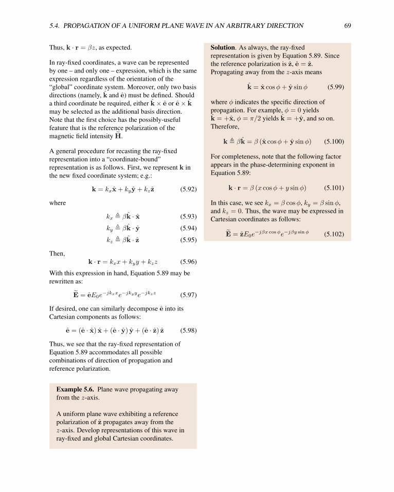
5.4. PROPAGATION OF A UNIFORM PLANE WAVE IN AN ARBITRARY DIRECTION 69
Thus, k · r = βz, as expected.
In ray-fixed coordinates, a wave can be represented
by one – and only one – expression, which is the same
expression regardless of the orientation of the
“global” coordinate system. Moreover, only two basis
directions (namely, k and e) must be defined. Should
a third coordinate be required, either k× e or e× k
may be selected as the additional basis direction.
Note that the first choice has the possibly-useful
feature that is the reference polarization of the
magnetic field intensity H.
A general procedure for recasting the ray-fixed
representation into a “coordinate-bound”
representation is as follows. First, we represent k in
the new fixed coordinate system; e.g.:
k = kxx+ kyy + kz z (5.92)
where
kx , βk · x (5.93)
ky , βk · y (5.94)
kz , βk · z (5.95)
Then,
k · r = kxx+ kyy + kzz (5.96)
With this expression in hand, Equation 5.89 may be
rewritten as:
E = eE0e−jkxxe−jkyye−jkzz (5.97)
If desired, one can similarly decompose e into its
Cartesian components as follows:
e = (e · x) x+ (e · y) y + (e · z) z (5.98)
Thus, we see that the ray-fixed representation of
Equation 5.89 accommodates all possible
combinations of direction of propagation and
reference polarization.
Example 5.6. Plane wave propagating away
from the z-axis.
A uniform plane wave exhibiting a reference
polarization of z propagates away from the
z-axis. Develop representations of this wave in
ray-fixed and global Cartesian coordinates.
Solution. As always, the ray-fixed
representation is given by Equation 5.89. Since
the reference polarization is z, e = z.
Propagating away from the z-axis means
k = x cosφ+ y sinφ (5.99)
where φ indicates the specific direction of
propagation. For example, φ = 0 yields
k = +x, φ = π/2 yields k = +y, and so on.
Therefore,
k , βk = β (x cosφ+ y sinφ) (5.100)
For completeness, note that the following factor
appears in the phase-determining exponent in
Equation 5.89:
k · r = β (x cosφ+ y sinφ) (5.101)
In this case, we see kx = β cosφ, ky = β sinφ,
and kz = 0. Thus, the wave may be expressed in
Cartesian coordinates as follows:
E = zE0e−jβx cosφe−jβy sinφ (5.102)
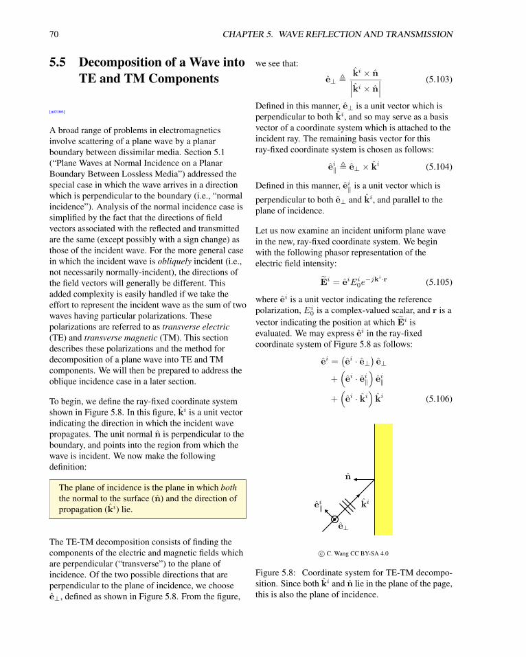
70 CHAPTER 5. WAVE REFLECTION AND TRANSMISSION
5.5 Decomposition of a Wave into
TE and TM Components
[m0166]
A broad range of problems in electromagnetics
involve scattering of a plane wave by a planar
boundary between dissimilar media. Section 5.1
(“Plane Waves at Normal Incidence on a Planar
Boundary Between Lossless Media”) addressed the
special case in which the wave arrives in a direction
which is perpendicular to the boundary (i.e., “normal
incidence”). Analysis of the normal incidence case is
simplified by the fact that the directions of field
vectors associated with the reflected and transmitted
are the same (except possibly with a sign change) as
those of the incident wave. For the more general case
in which the incident wave is obliquely incident (i.e.,
not necessarily normally-incident), the directions of
the field vectors will generally be different. This
added complexity is easily handled if we take the
effort to represent the incident wave as the sum of two
waves having particular polarizations. These
polarizations are referred to as transverse electric
(TE) and transverse magnetic (TM). This section
describes these polarizations and the method for
decomposition of a plane wave into TE and TM
components. We will then be prepared to address the
oblique incidence case in a later section.
To begin, we define the ray-fixed coordinate system
shown in Figure 5.8. In this figure, ki is a unit vector
indicating the direction in which the incident wave
propagates. The unit normal n is perpendicular to the
boundary, and points into the region from which the
wave is incident. We now make the following
definition:
The plane of incidence is the plane in which both
the normal to the surface (n) and the direction of
propagation (ki) lie.
The TE-TM decomposition consists of finding the
components of the electric and magnetic fields which
are perpendicular (“transverse”) to the plane of
incidence. Of the two possible directions that are
perpendicular to the plane of incidence, we choose
e⊥, defined as shown in Figure 5.8. From the figure,
we see that:
e⊥ ,ki × n∣∣∣ki × n
∣∣∣(5.103)
Defined in this manner, e⊥ is a unit vector which is
perpendicular to both ki, and so may serve as a basis
vector of a coordinate system which is attached to the
incident ray. The remaining basis vector for this
ray-fixed coordinate system is chosen as follows:
ei‖ , e⊥ × ki (5.104)
Defined in this manner, ei‖ is a unit vector which is
perpendicular to both e⊥ and ki, and parallel to the
plane of incidence.
Let us now examine an incident uniform plane wave
in the new, ray-fixed coordinate system. We begin
with the following phasor representation of the
electric field intensity:
Ei = eiEi0e−jki·r (5.105)
where ei is a unit vector indicating the reference
polarization, Ei0 is a complex-valued scalar, and r is a
vector indicating the position at which Ei is
evaluated. We may express ei in the ray-fixed
coordinate system of Figure 5.8 as follows:
ei =(ei · e⊥
)e⊥
+(ei · ei‖
)ei‖
+(ei · ki
)ki (5.106)
c© C. Wang CC BY-SA 4.0
Figure 5.8: Coordinate system for TE-TM decompo-
sition. Since both ki and n lie in the plane of the page,
this is also the plane of incidence.
5.5. DECOMPOSITION OF A WAVE INTO TE AND TM COMPONENTS 71
The electric field vector is always perpendicular to the
direction of propagation, so ei · ki = 0. This leaves:
ei =(ei · e⊥
)e⊥ +
(ei · ei‖
)ei‖ (5.107)
Substituting this expression into Equation 5.105, we
obtain:
Ei = e⊥EiTEe
−jki·r + ei‖EiTMe
−jki·r (5.108)
where
EiTE , Ei0 ei · e⊥ (5.109)
EiTM , Ei0 ei · ei‖ (5.110)
The first term in Equation 5.108 is the transverse
electric (TE) component of Ei, so-named because it is
the component which is perpendicular to the plane of
incidence. The second term in Equation 5.108 is the
transverse magnetic (TM) component of Ei. The term
“TM” refers to the fact that the magnetic field
associated with this component of the electric field is
perpendicular to the plane of incidence. This is
apparent since the magnetic field vector is
perpendicular to both the direction of propagation and
the electric field vector.
Summarizing:
The TE component is the component for which
Ei is perpendicular to the plane of incidence.
The TM component is the component for which
Hi is perpendicular to the plane of incidence;
i.e., the component for which Ei is parallel to the
plane of incidence.
Finally, observe that the total wave is the sum of its
TE and TM components. Therefore, we may analyze
the TE and TM components separately, and know that
the result for the combined wave is simply the sum of
the results for the TE and TM components.
As stated at the beginning of this section, the utility of
the TE-TM decomposition is that it simplifies the
analysis of wave reflection. This is because the
analysis of the TE and TM cases is relatively simple,
whereas direct analysis of the scattering of
arbitrarily-polarized waves is relatively difficult.
Note that the nomenclature “TE” and “TM” is
commonly but not universally used. Sometimes “TE”
is referred to as “perpendicular” polarization,
indicated using the subscript “⊥” or “s” (short for
senkrecht, German for “perpendicular”).
Correspondingly, “TM” is sometimes referred to as
“parallel” polarization, indicated using the subscript
“‖” or “p.”
Also, note that the TE component and TM component
are sometimes referred to as the TE mode and TM
mode, respectively. While the terms “component” and
“mode” are synonymous for the single plane wave
scenarios considered in this section, the terms are not
synonymous in general. For example, the wave inside
a waveguide may consist of multiple unique TE
modes which collectively comprise the TE component
of the field, and similarly the wave inside a waveguide
may consist of multiple unique TM modes which
collectively comprise the TM component of the field.
Finally, consider what happens when a plane wave is
normally-incident upon the boundary; i.e., when
ki = −n. In this case, Equation 5.103 indicates that
e⊥ = 0, so the TE-TM decomposition is undefined.
The situation is simply that both Ei and Hi are
already both perpendicular to the boundary, and there
is no single plane that can be uniquely identified as
the plane of incidence. We refer to this case as
transverse electromagnetic (TEM).
A wave which is normally-incident on a planar
surface is said to be transverse electromagnetic
(TEM) with respect to that boundary. There is no
unique TE-TM decomposition in this case.
The fact that a unique TE-TM decomposition does
not exist in the TEM case is of no consequence,
because the TEM case is easily handled as a separate
condition (see Section 5.1).

72 CHAPTER 5. WAVE REFLECTION AND TRANSMISSION
5.6 Plane Waves at Oblique
Incidence on a Planar
Boundary: TE Case
[m0167]
In this section, we consider the problem of reflection
and transmission from a planar boundary between
semi-infinite media for a transverse electric (TE)
uniform plane wave. Before attempting this section, a
review of Sections 5.1 (“Plane Waves at Normal
Incidence on a Planar Boundary Between Lossless
Media”) and 5.5 (“Decomposition of a Wave into TE
and TM Components”) is recommended. Also, note
that this section has much in common with
Section 5.7 (“Plane Waves at Oblique Incidence on a
Planar Boundary: TM Case”), although it is
recommended to attempt the TE case first.
The TE case is illustrated in Figure 5.9. The boundary
between the two semi-infinite and lossless regions is
located at the z = 0 plane. The wave is incident from
Region 1. The electric field intensity EiTE of this
wave is given by
EiTE(r) = yEiTEe−jki·r (5.111)
In this expression, r is the position at which EiTE is
evaluated, and
ki = kiβ1 (5.112)
c© C. Wang CC BY-SA 4.0
Figure 5.9: A TE uniform plane wave obliquely inci-
dent on the planar boundary between two semi-infinite
material regions.
where ki is the unit vector indicating the direction of
propagation and β1 = ω√µ1ǫ1 is the phase
propagation constant in Region 1. EiTE serves as the
“stimulus” in this problem, so all other contributions
to the total field will be expressed in terms of
quantities appearing in Equation 5.111.
The presence of reflected and transmitted uniform
plane waves is inferred from our experience with the
normal incidence scenario (Section 5.1). There, as
here, the symmetry of the problem indicates that the
reflected and transmitted components of the electric
field will have the same polarization as that of the
incident electric field. This is because there is nothing
present in the problem that could account for a change
in polarization. Thus, the reflected and transmitted
fields will also be TE. Therefore, we postulate the
following expression for the reflected wave:
Er(r) = yBe−jkr·r (5.113)
where B is an unknown, possibly complex-valued
constant to be determined and
kr = krβ1 (5.114)
indicates the direction of propagation, which is also
currently unknown.
Similarly, we postulate the following expression for
the transmitted wave:
Et(r) = yCe−jkt·r (5.115)
where C is an unknown, possibly complex-valued
constant to be determined;
kt = ktβ2 (5.116)
where kt is the unit vector indicating the direction of
propagation; and β2 = ω√µ2ǫ2 is the phase
propagation constant in Region 2.
At this point, the unknowns in this problem are the
constants B and C, as well as the directions kr and
kt. We may establish a relationship between EiTE , B,
and C by application of boundary conditions at
z = 0. First, recall that the tangential component of
the total electric field intensity must be continuous
across material boundaries. To apply this boundary
condition, let us define E1 and E2 to be the total
electric fields in Regions 1 and 2, respectively. The

5.6. PLANE WAVES AT OBLIQUE INCIDENCE ON A PLANAR BOUNDARY: TE CASE 73
total field in Region 1 is the sum of incident and
reflected fields, so
E1(r) = EiTE(r) + Er(r) (5.117)
The total field in Region 2 is simply
E2(r) = Et(r) (5.118)
Next, note that all electric field components are
already tangent to the boundary. Thus, continuity of
the tangential component of the electric field across
the boundary requires E1(0) = E2(0), and therefore
EiTE(r0) + Er(r0) = Et(r0) (5.119)
where r = r0 , xx+ yy since z = 0 on the
boundary. Now employing Equations 5.111, 5.113,
and 5.115, we obtain:
yEiTEe−jki·r0+yBe−jk
r·r0 = yCe−jkt·r0 (5.120)
Dropping the vector (y) since it is the same in each
term, we obtain:
EiTEe−jki·r0 +Be−jk
r·r0 = Ce−jkt·r0 (5.121)
For Equation 5.121 to be true at every point r0 on the
boundary, it must be true that
ki · r0 = kr · r0 = kt · r0 (5.122)
Essentially, we are requiring the phases of each field
in Regions 1 and 2 to be matched at every point along
the boundary. Any other choice will result in a
violation of boundary conditions at some point along
the boundary. This phase matching criterion will
determine the directions of propagation of the
reflected and transmitted fields, which we shall do
later.
First, let us use the phase matching criterion to
complete the solution for the coefficients B and C.
Enforcing Equation 5.122, we observe that
Equation 5.121 reduces to:
EiTE +B = C (5.123)
A second equation is needed since we currently have
only one equation (Equation 5.123) and two
unknowns (B and C). The second equation is
c© C. Wang CC BY-SA 4.0
Figure 5.10: Incident, reflected, and transmitted mag-
netic field components associated with the TE electric
field components shown in Figure 5.9.
obtained by applying the appropriate boundary
conditions to the magnetic field. The magnetic field
associated with each of the electric field components
is identified in Figure 5.10. Note the orientations of
the magnetic field vectors may be confirmed using the
plane wave relationships: Specifically, the cross
product of the electric and magnetic fields should
point in the direction of propagation. Expressions for
each of the magnetic field components is determined
formally below.
From the plane wave relationships, we determine that
the incident magnetic field intensity is
Hi(r) =1
η1ki × EiTE (5.124)
where η1 =√µ1/ǫ1 is the wave impedance in
Region 1. To make progress requires that we express
ki in the global fixed coordinate system. Here it is:
ki = x sinψi + z cosψi (5.125)
Thus:
Hi(r) =(z sinψi − x cosψi
) EiTEη1
e−jki·r (5.126)
Similarly, we determine that the reflected magnetic
field has the form:
Hr(r) =1
η1kr × Er (5.127)
74 CHAPTER 5. WAVE REFLECTION AND TRANSMISSION
In the global coordinate system:
kr = x sinψr − z cosψr (5.128)
Thus:
Hr(r) = (z sinψr + x cosψr)B
η1e−jk
r·r (5.129)
The transmitted magnetic field has the form:
Ht(r) =1
η2kt × Et (5.130)
In the global coordinate system:
kt = x sinψt + z cosψt (5.131)
Thus:
Ht(r) =(z sinψt − x cosψt
) Cη2e−jk
t·r (5.132)
The total magnetic field in Region 1 is the sum of
incident and reflected fields, so
H1(r) = Hi(r) + Hr(r) (5.133)
The magnetic field in Region 2 is simply
H2(r) = Ht(r) (5.134)
Since there is no current on the boundary, the
tangential component of the total magnetic field
intensity must be continuous across the boundary.
Expressed in terms of the quantities already
established, this boundary condition requires:
x · Hi(r0) + x · Hr(r0) = x · Ht(r0) (5.135)
where “x·” selects the component of the magnetic
field that is tangent to the boundary. Evaluating this
expression, we obtain:
−(cosψi
) EiTEη1
e−jki·r0
+ (cosψr)B
η1e−jk
r·r0
=−(cosψt
) Cη2e−jk
t·r0 (5.136)
Now employing the phase matching condition
expressed in Equation 5.122, we find:
−(cosψi
) EiTEη1
+ (cosψr)B
η1
=−(cosψt
) Cη2
(5.137)
Equations 5.123 and 5.137 comprise a linear system
of equations with unknowns B and C. This system of
equations is easily solved for B as follows. First, use
Equation 5.123 to eliminate C in Equation 5.137. The
result is:
−(cosψi
) EiTEη1
+ (cosψr)B
η1
=−(cosψt
) EiTE +B
η2(5.138)
Solving this equation for B, we obtain:
B =η2 cosψ
i − η1 cosψt
η2 cosψr + η1 cosψtEiTE (5.139)
We can express this result as a reflection coefficient as
follows:
B = ΓTEEiTE (5.140)
where
ΓTE ,η2 cosψ
i − η1 cosψt
η2 cosψr + η1 cosψt(5.141)
It is worth noting that Equation 5.141 becomes the
reflection coefficient for normal (TEM) incidence
when ψi = ψr = ψt = 0, as expected.
Returning to Equation 5.123, we now find
C = (1 + ΓTE)EiTE (5.142)
Let us now summarize the solution. Given the TE
electric field intensity expressed in Equation 5.111,
we find:
Er(r) = yΓTEEiTEe
−jkr·r (5.143)
Et(r) = y (1 + ΓTE)EiTEe
−jkt·r (5.144)
This solution is complete except that we have not yet
determined kr, which is now completely determined
by ψr via Equation 5.128, and kt, which is now
completely determined by ψt via Equation 5.131. In
other words, we have not yet determined the
directions of propagation ψr for the reflected wave
and ψt for the transmitted wave. However, ψr and ψi
can be found using Equation 5.122. Here we shall
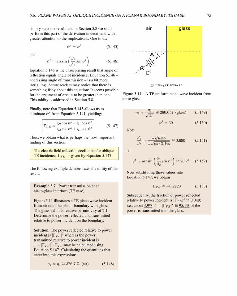
5.6. PLANE WAVES AT OBLIQUE INCIDENCE ON A PLANAR BOUNDARY: TE CASE 75
simply state the result, and in Section 5.8 we shall
perform this part of the derivation in detail and with
greater attention to the implications. One finds:
ψr = ψi (5.145)
and
ψt = arcsin
(β1β2
sinψi)
(5.146)
Equation 5.145 is the unsurprising result that angle of
reflection equals angle of incidence. Equation 5.146 –
addressing angle of transmission – is a bit more
intriguing. Astute readers may notice that there is
something fishy about this equation: It seems possible
for the argument of arcsin to be greater than one.
This oddity is addressed in Section 5.8.
Finally, note that Equation 5.145 allows us to
eliminate ψr from Equation 5.141, yielding:
ΓTE =η2 cosψ
i − η1 cosψt
η2 cosψi + η1 cosψt(5.147)
Thus, we obtain what is perhaps the most important
finding of this section:
The electric field reflection coefficient for oblique
TE incidence, ΓTE , is given by Equation 5.147.
The following example demonstrates the utility of this
result.
Example 5.7. Power transmission at an
air-to-glass interface (TE case).
Figure 5.11 illustrates a TE plane wave incident
from air onto the planar boundary with glass.
The glass exhibits relative permittivity of 2.1.
Determine the power reflected and transmitted
relative to power incident on the boundary.
Solution. The power reflected relative to power
incident is |ΓTE |2 whereas the power
transmitted relative to power incident is
1− |ΓTE |2. ΓTE may be calculated using
Equation 5.147. Calculating the quantities that
enter into this expression:
η1 ≈ η0 ∼= 376.7 Ω (air) (5.148)
c© C. Wang CC BY-SA 4.0
Figure 5.11: A TE uniform plane wave incident from
air to glass.
η2 ≈ η0√2.1
∼= 260.0 Ω (glass) (5.149)
ψi = 30 (5.150)
Note
β1β2
≈ ω√µ0ǫ0
ω√µ0 · 2.1ǫ0
∼= 0.690 (5.151)
so
ψt = arcsin
(β1β2
sinψi)
∼= 20.2 (5.152)
Now substituting these values into
Equation 5.147, we obtain
ΓTE ∼= −0.2220 (5.153)
Subsequently, the fraction of power reflected
relative to power incident is |ΓTE |2 ∼= 0.049;
i.e., about 4.9%. 1− |ΓTE |2 ∼= 95.1% of the
power is transmitted into the glass.

76 CHAPTER 5. WAVE REFLECTION AND TRANSMISSION
5.7 Plane Waves at Oblique
Incidence on a Planar
Boundary: TM Case
[m0164]
In this section, we consider the problem of reflection
and transmission from a planar boundary between
semi-infinite media for a transverse magnetic (TM)
uniform plane wave. Before attempting this section, a
review of Sections 5.1 (“Plane Waves at Normal
Incidence on a Planar Boundary Between Lossless
Media”) and 5.5 (“Decomposition of a Wave into TE
and TM Components”) is recommended. Also, note
that this section has much in common with
Section 5.6 (“Plane Waves at Oblique Incidence on a
Planar Boundary: TE Case”), and it is recommended
to attempt the TE case first.
In this section, we consider the scenario illustrated in
Figure 5.12. The boundary between the two
semi-infinite and lossless regions is located at the
z = 0 plane. The wave is incident from Region 1. The
magnetic field intensity HiTM of this wave is given by
HiTM (r) = yHi
TMe−jki·r (5.154)
In this expression, r is the position at which HiTM is
c© C. Wang CC BY-SA 4.0
Figure 5.12: A TM uniform plane wave obliquely
incident on the planar boundary between two semi-
infinite material regions.
evaluated. Also,
ki = kiβ1 (5.155)
where ki is the unit vector indicating the direction of
propagation and β1 = ω√µ1ǫ1 is the phase
propagation constant in Region 1. HiTM serves as the
“stimulus” in this problem, and all other contributions
to the total field may be expressed in terms of
parameters associated with Equation 5.154.
The presence of reflected and transmitted uniform
plane waves is inferred from our experience with the
normal incidence scenario (Section 5.1). There, as
here, the symmetry of the problem indicates that the
reflected and transmitted components of the magnetic
field will have the same polarization as that of the
incident electric field. This is because there is nothing
present in the problem that could account for a
change in polarization. Thus, the reflected and
transmitted fields will also be TM. So we postulate
the following expression for the reflected wave:
Hr(r) = −yBe−jkr·r (5.156)
where B is an unknown, possibly complex-valued
constant to be determined and
kr = krβ1 (5.157)
indicates the direction of propagation.
The reader may wonder why we have chosen −y, as
opposed to +y, as the reference polarization for Hr.
In fact, either +y or −y could be used. However, the
choice is important because the form of the results we
obtain in this section – specifically, the reflection
coefficient – will be determined with respect to this
specific convention, and will be incorrect with respect
to the opposite convention. We choose −y because it
has a particular advantage which we shall point out at
the end of this section.
Continuing, we postulate the following expression for
the transmitted wave:
Ht(r) = yCe−jkt·r (5.158)
where C is an unknown, possibly complex-valued
constant to be determined and
kt = ktβ2 (5.159)

5.7. PLANE WAVES AT OBLIQUE INCIDENCE ON A PLANAR BOUNDARY: TM CASE 77
where kt is the unit vector indicating the direction of
propagation and β2 = ω√µ2ǫ2 is the phase
propagation constant in Region 2.
At this point, the unknowns in this problem are the
constants B and C, as well as the unknown directions
kr and kt. We may establish a relationship between
HiTM , B, and C by application of boundary
conditions at z = 0. First, we presume no impressed
current at the boundary. Thus, the tangential
component of the total magnetic field intensity must
be continuous across the boundary. To apply this
boundary condition, let us define H1 and H2 to be the
total magnetic fields in Regions 1 and 2, respectively.
The total field in Region 1 is the sum of incident and
reflected fields, so
H1(r) = HiTM (r) + Hr(r) (5.160)
The field in Region 2 is simply
H2(r) = Ht(r) (5.161)
Also, we note that all magnetic field components are
already tangent to the boundary. Thus, continuity of
the tangential component of the magnetic field across
the boundary requires H1(r0) = H2(r0), where
r0 , xx+ yy since z = 0 on the boundary.
Therefore,
HiTM (r0) + Hr(r0) = Ht(r0) (5.162)
Now employing Equations 5.154, 5.156, and 5.158,
we obtain:
yHiTMe
−jki·r0 − yBe−jkr·r0 = yCe−jk
t·r0
(5.163)
Dropping the vector (y) since it is the same in each
term, we obtain:
HiTMe
−jki·r0 −Be−jkr·r0 = Ce−jk
t·r0 (5.164)
For this to be true at every point r0 on the boundary, it
must be true that
ki · r0 = kr · r0 = kt · r0 (5.165)
Essentially, we are requiring the phases of each field
in Regions 1 and 2 to be matched at every point along
the boundary. Any other choice will result in a
violation of boundary conditions at some point along
the boundary. This expression allows us to solve for
the directions of propagation of the reflected and
transmitted fields, which we shall do later. Our
priority for now shall be to solve for the coefficients
B and C.
Enforcing Equation 5.165, we observe that
Equation 5.164 reduces to:
HiTM −B = C (5.166)
A second equation is needed since we currently have
only one equation (Equation 5.166) and two
unknowns (B and C). The second equation is
obtained by applying the appropriate boundary
conditions to the electric field. The electric field
associated with each of the magnetic field
components is identified in Figure 5.12. Note the
orientations of the electric field vectors may be
confirmed using the plane wave relationships:
Specifically, the cross product of the electric and
magnetic fields should point in the direction of
propagation. Expressions for each of the electric field
components is determined formally below.
From the plane wave relationships, we determine that
the incident electric field intensity is
Ei(r) = −η1ki × HiTM (5.167)
where η1 =√µ1/ǫ1 is the wave impedance in
Region 1. To make progress requires that we express
ki in the global fixed coordinate system. Here it is:
ki = x sinψi + z cosψi (5.168)
Thus:
Ei(r) =(x cosψi − z sinψi
)η1H
iTMe
−jki·r
(5.169)
Similarly we determine that the reflected electric field
has the form:
Er(r) = −η1kr × Hr (5.170)
In the global coordinate system:
kr = x sinψr − z cosψr (5.171)
Thus:
Er(r) = (x cosψr + z sinψr) η1Be−jkr·r (5.172)

78 CHAPTER 5. WAVE REFLECTION AND TRANSMISSION
The transmitted magnetic field has the form:
Et(r) = −η2kt × Ht (5.173)
In the global coordinate system:
kt = x sinψt + z cosψt (5.174)
Thus:
Et(r) =(x cosψt − z sinψt
)η2Ce
−jkt·r (5.175)
The total electric field in Region 1 is the sum of
incident and reflected fields, so
E1(r) = Ei(r) + Er(r) (5.176)
The electric field in Region 2 is simply
E2(r) = Et(r) (5.177)
The tangential component of the total electric field
intensity must be continuous across the boundary.
Expressed in terms of the quantities already
established, this boundary condition requires:
x · Ei(r0) + x · Er(r0) = x · Et(r0) (5.178)
where “x·” selects the component of the electric field
that is tangent to the boundary. Evaluating this
expression, we obtain:
+(cosψi
)η1H
iTMe
−jki·r0
+ (cosψr) η1Be−jkr·r0
=+(cosψt
)η2Ce
−jkt·r0 (5.179)
Now employing the “phase matching” condition
expressed in Equation 5.165, we find:
+(cosψi
)η1H
iTM
+ (cosψr) η1B
=+(cosψt
)η2C (5.180)
Equations 5.166 and 5.180 comprise a linear system
of equations with unknowns B and C. This system of
equations is easily solved for B as follows. First, use
Equation 5.166 to eliminate C in Equation 5.180. The
result is:
+(cosψi
)η1H
iTM
+ (cosψr) η1B
=+(cosψt
)η2(HiTM −B
)(5.181)
Solving this equation for B, we obtain:
B =−η1 cosψi + η2 cosψ
t
+η1 cosψr + η2 cosψtHiTM (5.182)
We can express this result as follows:
B = ΓTMHiTM (5.183)
where we have made the definition
ΓTM ,−η1 cosψi + η2 cosψ
t
+η1 cosψr + η2 cosψt(5.184)
We are now able to express the complete solution in
terms of the electric field intensity. First we make the
substitution EiTM , η1HiTM in Equation 5.169,
yielding:
Ei(r) =(x cosψi − z sinψi
)EiTMe
−jki·r (5.185)
The factor η1B in Equation 5.172 becomes
ΓTMEiTM , so we obtain:
Er(r) = (x cosψr + z sinψr)
· ΓTMEiTMe−jkr·r (5.186)
Thus, we see ΓTM is the reflection coefficient for the
electric field intensity.
Returning to Equation 5.166, we now find
C = HiTM −B
= HiTM − ΓTMH
iTM
= (1− ΓTM )HiTM
= (1− ΓTM )EiTM/η1 (5.187)
Subsequently, Equation 5.175 becomes
Et(r) =(x cosψt − z sinψt
)
· (1− ΓTM )η2η1EiTMe
−jkt·r (5.188)
This solution is complete except that we have not yet
determined kr, which is now completely determined
by ψr via Equation 5.171, and kt, which is now
completely determined by ψt via Equation 5.174. In
other words, we have not yet determined the
directions of propagation ψr for the reflected wave
and ψt for the transmitted wave. However, ψr and ψi

5.7. PLANE WAVES AT OBLIQUE INCIDENCE ON A PLANAR BOUNDARY: TM CASE 79
can be found using Equation 5.165. Here we shall
simply state the result, and in Section 5.8 we shall
perform this part of the derivation in detail and with
greater attention to the implications. One finds:
ψr = ψi (5.189)
i.e., angle of reflection equals angle of incidence.
Also,
ψt = arcsin
(β1β2
sinψi)
(5.190)
Astute readers may notice that there is something
fishy about Equation 5.190. Namely, it seems possible
for the argument of arcsin to be greater than one.
This oddity is addressed in Section 5.8.
Now let us return to the following question, raised
near the beginning of this section: Why choose −y, as
opposed to +y, as the reference polarization for Hr,
as shown in Figure 5.12? To answer this question,
first note that ΓTM (Equation 5.184) becomes the
reflection coefficient for normal (TEM) incidence
when ψi = ψt = 0. If we had chosen +y as the
reference polarization for Hr, we would have instead
obtained an expression for ΓTM that has the opposite
sign for TEM incidence.3 There is nothing wrong
with this answer, but it is awkward to have different
values of the reflection coefficient for the same
physical scenario. By choosing −y, the reflection
coefficient for the oblique incidence case computed
for ψi = 0 converges to the reflection coefficient
previously computed for the normal-incidence case. It
is important to be aware of this issue, as one
occasionally encounters work in which the opposite
(“+y”) reference polarization has been employed.
Finally, note that Equation 5.189 allows us to
eliminate ψr from Equation 5.184, yielding:
ΓTM =−η1 cosψi + η2 cosψ
t
+η1 cosψi + η2 cosψt(5.191)
Thus, we obtain what is perhaps the most important
finding of this section:
The electric field reflection coefficient for oblique
TM incidence, ΓTM , is given by Equation 5.191.
3Obtaining this result is an excellent way for the student to con-
firm their understanding of the derivation presented in this section.
The following example demonstrates the utility of this
result.
Example 5.8. Power transmission at an
air-to-glass interface (TM case).
Figure 5.13 illustrates a TM plane wave incident
from air onto the planar boundary with a glass
region. The glass exhibits relative permittivity of
2.1. Determine the power reflected and
transmitted relative to power incident on the
boundary.
Solution. The power reflected relative to power
incident is |ΓTM |2 whereas the power
transmitted relative to power incident is
1− |ΓTM |2. ΓTM may be calculated using
Equation 5.191. Calculating the quantities that
enter into this expression:
η1 ≈ η0 ∼= 376.7 Ω (air) (5.192)
η2 ≈ η0√2.1
∼= 260.0 Ω (glass) (5.193)
ψi = 30 (5.194)
Note
β1β2
≈ ω√µ0ǫ0
ω√µ0 · 2.1ǫ0
∼= 0.690 (5.195)
so
ψt = arcsin
(β1β2
sinψi)
∼= 20.2 (5.196)
Now substituting these values into
Equation 5.191, we obtain
ΓTM ∼= −0.1442 (5.197)
(Did you get an answer closer to −0.1323? If so,
you probably did not use sufficient precision to
represent intermediate results. This is a good
example of a problem in which three significant
figures for results that are used in subsequent
calculations is not sufficient.)
The fraction of power reflected relative to power
incident is now determined to be

80 CHAPTER 5. WAVE REFLECTION AND TRANSMISSION
c© C. Wang CC BY-SA 4.0
Figure 5.13: A TM uniform plane wave incident from
air to glass.
|ΓTM |2 ∼= 0.021; i.e., about 2.1%.
1− |ΓTM |2 ∼= 97.9% of the power is transmitted
into the glass.
Note that the result obtained in the preceding example
is different from the result for a TE wave incident
from the same direction (Example 5.7). In other
words:
The fraction of power reflected and transmitted
from the planar boundary between dissimilar me-
dia depends on the polarization of the incident
wave relative to the boundary, as well as the an-
gle of incidence.
5.8 Angles of Reflection and
Refraction
[m0168]
Consider the situation shown in Figure 5.14: A
uniform plane wave obliquely incident on the planar
boundary between two semi-infinite material regions.
Let a point on the boundary be represented as the
position vector
r0 = xx+ yy (5.198)
In both Sections 5.6 (“Plane Waves at Oblique
Incidence on a Planar Boundary: TE Case”) and 5.7
(“Plane Waves at Oblique Incidence on a Planar
Boundary: TM Case”), it is found that
ki · r0 = kr · r0 = kt · r0 (5.199)
In this expression,
ki = β1ki (5.200)
kr = β1kr (5.201)
kt = β2kt (5.202)
where ki, kr, and kt are unit vectors in the direction
of incidence, reflection, and transmission,
c© C. Wang CC BY-SA 4.0
Figure 5.14: A uniform plane wave obliquely inci-
dent on the planar boundary between two semi-infinite
material regions.
5.8. ANGLES OF REFLECTION AND REFRACTION 81
respectively; and β1 and β2 are the phase propagation
constants in Region 1 (from which the wave is
incident) and Region 2, respectively. Equation 5.199
is essentially a boundary condition that enforces
continuity of the phase of the electric and magnetic
fields across the boundary, and is sometimes referred
to as the “phase matching” requirement. Since the
same requirement emerges independently in the TE
and TM cases, and since any plane wave may be
decomposed into TE and TM components, the
requirement must apply to any incident plane wave
regardless of polarization.
Equation 5.199 is the key to finding the direction of
reflection ψr and direction of transmission ψt. First,
observe:
ki = x sinψi + z cosψi (5.203)
kr = x sinψr − z cosψr (5.204)
kt = x sinψt + z cosψt (5.205)
Therefore, we may express Equation 5.199 in the
following form
β1(x sinψi + z cosψi
)· (xx+ yy)
= β1 (x sinψr − z cosψr) · (xx+ yy)
= β2(x sinψt + z cosψt
)· (xx+ yy) (5.206)
which reduces to
β1 sinψi = β1 sinψ
r = β2 sinψt (5.207)
Examining the first and second terms of
Equation 5.207, and noting that ψi and ψr are both
limited to the range −π/2 to +π/2, we find that:
ψr = ψi (5.208)
In plain English:
Angle of reflection equals angle of incidence.
Examining the first and third terms of Equation 5.207,
we find that
β1 sinψi = β2 sinψ
t (5.209)
Since β1 = ω√µ1ǫ1 and β2 = ω
√µ2ǫ2,
Equation 5.209 expressed explicitly in terms of the
constitutive parameters is:
√µ1ǫ1 sinψ
i =√µ2ǫ2 sinψ
t (5.210)
Thus, we see that ψt does not depend on frequency,
except to the extent that the constitutive parameters
might. We may also express this relationship in terms
of the relative values of constitutive parameters; i.e.,
µ1 = µr1µ0, ǫ1 = ǫr1ǫ0, µ2 = µr2µ0, and
ǫ2 = ǫr2ǫ0. In terms of the relative parameters:
√µr1ǫr1 sinψ
i =√µr2ǫr2 sinψ
t (5.211)
This is known as Snell’s law or the law of refraction.
Refraction is simply transmission with the result that
the direction of propagation is changed.
Snell’s law (Equation 5.211) determines the an-
gle of refraction (transmission).
The associated formula for ψt explicitly is:
ψt = arcsin
(√µr1ǫr1µr2ǫr2
sinψi)
(5.212)
For the common special case of non-magnetic media,
one assumes µr1 = µr2 = 1. In this case, Snell’s law
simplifies to:
√ǫr1 sinψ
i =√ǫr2 sinψ
t (5.213)
In optics, it is common to express permittivities in
terms of indices of refraction; e.g., n1 ,√ǫr1 and
n2 ,√ǫr2. Thus, Snell’s law in optics is often
expressed as:
n1 sinψi = n2 sinψ
t (5.214)
When both media are non-magnetic, Equation 5.212
simplifies to
ψt = arcsin
(√ǫr1ǫr2
sinψi)
(5.215)
When ǫr2 > ǫr1, we observe that ψt < ψi. In other
words, the transmitted wave travels in a direction that
is closer to the surface normal than the angle of
incidence. This scenario is demonstrated in the
following example.
Example 5.9. Refraction of light at an air-glass
boundary.
Figure 5.15 shows a narrow beam of light that is
incident from air to glass at an angle ψi = 60.

82 CHAPTER 5. WAVE REFLECTION AND TRANSMISSION
c© Z. Sandor CC BY-SA 3.0
Figure 5.15: Angles of reflection and refraction for a
light wave incident from air onto glass.
As expected, the angle of reflection ψr is
observed to be equal to ψi. The angle of
refraction ψt is observed to be 35. What is the
relative permittivity of the glass?
Solution. Since the permittivity of glass is
greater than that of air, we observe the expected
result ψt < ψi. Since glass is non-magnetic, the
expected relationship between these angles is
given by Equation 5.213. Solving that equation
for the relative permittivity of the glass, we
obtain:
ǫr2 = ǫr1
(sinψi
sinψt
)2
∼= 2.28 (5.216)
When a wave travels in the reverse direction – i.e.,
from a non-magnetic medium of higher permittivity
to a medium of lower permittivity – one finds
ψt > ψr. In other words, the refraction is away from
the surface normal. Figure 5.16 shows an example
from common experience.
In non-magnetic media, when ǫr1 < ǫr2, ψt <ψi (refraction toward the surface normal). When
ǫr1 > ǫr2, ψt > ψi (refraction away from the
surface normal).
c© G. Saini CC BY-SA 4.0
Figure 5.16: Refraction accounts for the apparent dis-
placement of an underwater object from the perspec-
tive of an observer above the water.
Under certain conditions, the ǫr2 < ǫr1 case leads to
the following surprising observation: When
calculating ψt using, for example, Equation 5.212,
one finds that√ǫr1/ǫr2 sinψ
i can be greater than 1.
Since the sin function yields values between −1 and
+1, the result of the arcsin function is undefined.
This odd situation is addressed in Section 5.11. For
now, we will simply note that this condition leads to
the phenomenon of total internal reflection. For now,
all we can say is that when ǫr2 < ǫr1, ψt is able to
reach π/2 radians, which corresponds to propagation
parallel to the boundary. Beyond that threshold, we
must account for the unique physical considerations
associated with total internal reflection.
We conclude this section with a description of the
common waveguiding device known as the prism,
shown in Figure 5.17. This particular device uses
refraction to change the direction of light waves
(similar devices can be used to manipulate radio
waves as well). Many readers are familiar with the use
of prisms to separate white light into its constituent
colors (frequencies), as shown in Figure 5.18. The
separation of colors is due to frequency dependence
of the material comprising the prism. Specifically, the
permittivity of the material is a function of frequency,
and therefore the angle of refraction is a function of
frequency. Thus, each frequency is refracted by a
different amount. Conversely, a prism comprised of a
material whose permittivity exhibits negligible
variation with frequency will not separate incident

5.9. TE REFLECTION IN NON-MAGNETIC MEDIA 83
c© D-Kuru CC BY-SA 3.0
Figure 5.17: A typical triangular prism.
white light into its constituent colors since each color
will be refracted by the same amount.
Additional Reading:
• “Prism” on Wikipedia.
• “Refraction” on Wikipedia.
• “Refractive index” on Wikipedia.
• “Snell’s law” on Wikipedia.
• “Total internal reflection” on Wikipedia.
c© Suidroot CC BY-SA 4.0
Figure 5.18: A color-separating prism.
5.9 TE Reflection in
Non-magnetic Media
[m0171]
Figure 5.19 shows a TE uniform plane wave incident
on the planar boundary between two semi-infinite
material regions. In this case, the reflection coefficient
is given by:
ΓTE =η2 cosψ
i − η1 cosψt
η2 cosψi + η1 cosψt(5.217)
where ψi and ψt are the angles of incidence and
transmission (refraction), respectively; and η1 and η2are the wave impedances in Regions 1 and 2,
respectively. Many materials of practical interest are
non-magnetic; that is, they have permeability that is
not significantly different from the permeability of
free space. In this section, we consider the behavior
of the reflection coefficient for this class of materials.
To begin, recall the general form of Snell’s law:
sinψt =β1β2
sinψi (5.218)
In non-magnetic media, the permeabilities µ1 and µ2
are assumed equal to µ0. Thus:
β1β2
=ω√µ1ǫ1
ω√µ2ǫ2
=
√ǫ1ǫ2
(5.219)
c© C. Wang CC BY-SA 4.0
Figure 5.19: A TE uniform plane wave obliquely inci-
dent on the planar boundary between two semi-infinite
regions of lossless non-magnetic material.

84 CHAPTER 5. WAVE REFLECTION AND TRANSMISSION
Since permittivity ǫ can be expressed as ǫ0 times the
relative permittivity ǫr, we may reduce further to:
β1β2
=
√ǫr1ǫr2
(5.220)
Now Equation 5.218 reduces to:
sinψt =
√ǫr1ǫr2
sinψi (5.221)
Next, note that for any value ψ, one may write cosine
in terms of sine as follows:
cosψ =
√1− sin2 ψ (5.222)
Therefore,
cosψt =
√1− ǫr1
ǫr2sin2 ψi (5.223)
Also we note that in non-magnetic media
η1 =
õ1
ǫ1=
õ0
ǫr1ǫ0=
η0√ǫr1
(5.224)
η2 =
õ2
ǫ2=
õ0
ǫr2ǫ0=
η0√ǫr2
(5.225)
where η0 is the wave impedance in free space.
Making substitutions into Equation 5.217, we obtain:
ΓTE =
(η0/
√ǫr2)cosψi −
(η0/
√ǫr1)cosψt(
η0/√ǫr2)cosψi +
(η0/
√ǫr1)cosψt
(5.226)
Multiplying numerator and denominator by√ǫr2/η0,
we obtain:
ΓTE =cosψi −
√ǫr2/ǫr1 cosψ
t
cosψi +√ǫr2/ǫr1 cosψt
(5.227)
Finally, by substituting Equation 5.223, we obtain:
ΓTE =cosψi −
√ǫr2/ǫr1 − sin2 ψi
cosψi +√ǫr2/ǫr1 − sin2 ψi
(5.228)
This expression has the advantage that it is now
entirely in terms of ψi, with no need to first calculate
ψt.
Using Equation 5.228, we can see how different
combinations of material affect the reflection
-1
-0.5
0
0.5
1
0 10 20 30 40 50 60 70 80 90
2
10
100
Ref
lect
ion
Coe
ffici
ent
angle of incidence [deg]
Figure 5.20: The reflection coefficient ΓTE as a func-
tion of angle of incidence ψi for various media combi-
nations. Curves are labeled with the ratio ǫr2/ǫr1.
coefficient. First, we note that when ǫr1 = ǫr2 (i.e.,
same media on both sides of the boundary), ΓTE = 0as expected. When ǫr1 > ǫr2 (e.g., wave traveling in
glass toward air), we see that it is possible for
ǫr2/ǫr1 − sin2 ψi to be negative, which makes ΓTEcomplex-valued. This results in total internal
reflection, and is addressed elsewhere in another
section. When ǫr1 < ǫr2 (e.g., wave traveling in air
toward glass), we see that ǫr2/ǫr1 − sin2 ψi is always
positive, so ΓTE is always real-valued.
Let us continue with the ǫr1 < ǫr2 condition.
Figure 5.20 shows ΓTE plotted for various
combinations of media over all possible angles of
incidence from 0 (normal incidence) to π/2 (grazing
incidence). We observe:
In non-magnetic media with ǫr1 < ǫr2, ΓTE is
real-valued, negative, and decreases to −1 as ψi
approaches grazing incidence.
Also note that at any particular angle of incidence,
ΓTE trends toward −1 as ǫr2/ǫr1 increases. Thus, we
observe that as ǫr2/ǫr1 → ∞, the result is
increasingly similar to the result we would obtain for
a perfect conductor in Region 2.

5.10. TM REFLECTION IN NON-MAGNETIC MEDIA 85
5.10 TM Reflection in
Non-magnetic Media
[m0172]
Figure 5.21 shows a TM uniform plane wave incident
on the planar boundary between two semi-infinite
material regions. In this case, the reflection coefficient
is given by:
ΓTM =−η1 cosψi + η2 cosψ
t
+η1 cosψi + η2 cosψt(5.229)
where ψi and ψt are the angles of incidence and
transmission (refraction), respectively; and η1 and η2are the wave impedances in Regions 1 and 2,
respectively. Many materials of practical interest are
non-magnetic; that is, they have permeability that is
not significantly different from the permeability of
free space. In this section, we consider the behavior
of the reflection coefficient for this class of materials.
To begin, recall the general form of Snell’s law:
sinψt =β1β2
sinψi (5.230)
In non-magnetic media, the permeabilities µ1 and µ2
are assumed equal to µ0. Thus:
β1β2
=ω√µ1ǫ1
ω√µ2ǫ2
=
√ǫ1ǫ2
(5.231)
c© C. Wang CC BY-SA 4.0
Figure 5.21: A transverse magnetic uniform plane
wave obliquely incident on the planar boundary be-
tween two semi-infinite material regions.
Since permittivity ǫ can be expressed as ǫ0 times the
relative permittivity ǫr, we may reduce further to:
β1β2
=
√ǫr1ǫr2
(5.232)
Now Equation 5.230 reduces to:
sinψt =
√ǫr1ǫr2
sinψi (5.233)
Next, note that for any value ψ, one may write cosine
in terms of sine as follows:
cosψ =
√1− sin2 ψ (5.234)
Therefore,
cosψt =
√1− ǫr1
ǫr2sin2 ψi (5.235)
Also we note that in non-magnetic media
η1 =
õ1
ǫ1=
õ0
ǫr1ǫ0=
η0√ǫr1
(5.236)
η2 =
õ2
ǫ2=
õ0
ǫr2ǫ0=
η0√ǫr2
(5.237)
where η0 is the wave impedance in free space.
Making substitutions into Equation 5.229, we obtain:
ΓTM =−(η0/
√ǫr1)cosψi +
(η0/
√ǫr2)cosψt
+(η0/
√ǫr1)cosψi +
(η0/
√ǫr2)cosψt
(5.238)
Multiplying numerator and denominator by√ǫr2/η0,
we obtain:
ΓTM =−√ǫr2/ǫr1 cosψ
i + cosψt
+√ǫr2/ǫr1 cosψi + cosψt
(5.239)
Substituting Equation 5.235, we obtain:
ΓTM =−√ǫr2/ǫr1 cosψ
i +√
1− (ǫr1/ǫr2) sin2 ψi
+√ǫr2/ǫr1 cosψi +
√1− (ǫr1/ǫr2) sin
2 ψi
(5.240)
This expression has the advantage that it is now
entirely in terms of ψi, with no need to first calculate
ψt.
Finally, multiplying numerator and denominator by√ǫr2/ǫr1, we obtain:
ΓTM =− (ǫr2/ǫr1) cosψ
i +√ǫr2/ǫr1 − sin2 ψi
+(ǫr2/ǫr1) cosψi +√ǫr2/ǫr1 − sin2 ψi
(5.241)

86 CHAPTER 5. WAVE REFLECTION AND TRANSMISSION
-1
-0.5
0
0.5
1
0 10 20 30 40 50 60 70 80 90
2
10
100
Ref
lect
ion
Coe
ffici
ent
angle of incidence [deg]
Figure 5.22: The reflection coefficient ΓTM as a func-
tion of angle of incidence ψi for various media combi-
nations, parameterized as ǫr2/ǫr1.
Using Equation 5.241, we can easily see how
different combinations of material affect the reflection
coefficient. First, we note that when ǫr1 = ǫr2 (i.e.,
same media on both sides of the boundary), ΓTM = 0as expected. When ǫr1 > ǫr2 (e.g., wave traveling in
glass toward air), we see that it is possible for
ǫr2/ǫr1 − sin2 ψi to be negative, which makes ΓTMcomplex-valued. This results in total internal
reflection, and is addressed in another section. When
ǫr1 < ǫr2 (e.g., wave traveling in air toward glass),
we see that ǫr2/ǫr1 − sin2 ψi is always positive, so
ΓTM is always real-valued.
Let us continue with the ǫr1 < ǫr2 condition.
Figure 5.22 shows ΓTM plotted for various
combinations of media over all possible angles of
incidence from 0 (normal incidence) to π/2 (grazing
incidence). We observe:
In non-magnetic media with ǫr1 < ǫr2, ΓTM is
real-valued and increases from a negative value
for normal incidence to +1 as ψi approaches
grazing incidence.
Note that at any particular angle of incidence, ΓTMtrends toward −1 as ǫr2/ǫr1 → ∞. In this respect,
the behavior of the TM component is similar to that
of the TE component. In other words: As
c© C. Wang CC BY-SA 4.0
Figure 5.23: Reflection of a plane wave with angle of
incidence ψi equal to the polarizing angle ψiB . Here
the media are non-magnetic with ǫr1 < ǫr2.
ǫr2/ǫr1 → ∞, the result for both the TE and TM
components are increasingly similar to the result we
would obtain for a perfect conductor in Region 2.
Also note that when ǫr1 < ǫr2, ΓTM changes sign
from negative to positive as angle of incidence
increases from 0 to π/2. This behavior is quite
different from that of the TE component, which is
always negative for ǫr1 < ǫr2. The angle of incidence
at which ΓTM = 0 is referred to as Brewster’s angle,
which we assign the symbol ψiB . Thus:
ψiB , ψi at which ΓTM = 0 (5.242)
In the discussion that follows, here is the key point to
keep in mind:
Brewster’s angle ψiB is the angle of incidence at
which ΓTM = 0.
Brewster’s angle is also referred to as the polarizing
angle. The motivation for the term “polarizing angle”
is demonstrated in Figure 5.23. In this figure, a plane
wave is incident with ψi = ψiB . The wave may
contain TE and TM components in any combination.
Applying the principle of superposition, we may
consider these components separately. The TE
component of the incident wave will scatter as
reflected and transmitted waves which are also TE.
However, ΓTM = 0 when ψi = ψiB , so the TM
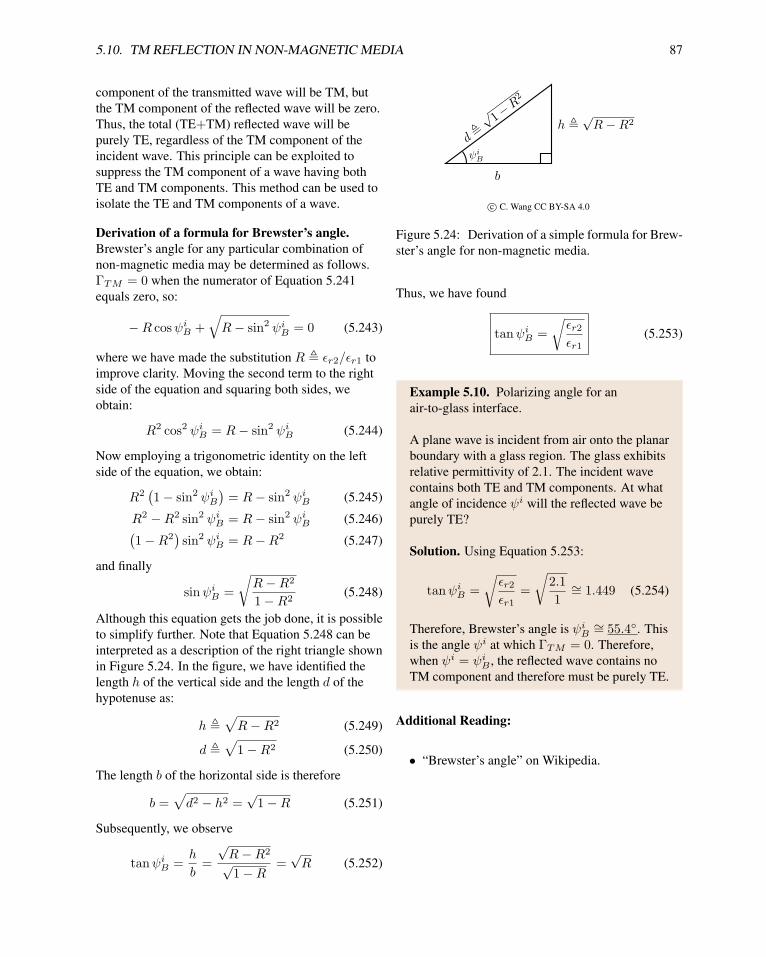
5.10. TM REFLECTION IN NON-MAGNETIC MEDIA 87
component of the transmitted wave will be TM, but
the TM component of the reflected wave will be zero.
Thus, the total (TE+TM) reflected wave will be
purely TE, regardless of the TM component of the
incident wave. This principle can be exploited to
suppress the TM component of a wave having both
TE and TM components. This method can be used to
isolate the TE and TM components of a wave.
Derivation of a formula for Brewster’s angle.
Brewster’s angle for any particular combination of
non-magnetic media may be determined as follows.
ΓTM = 0 when the numerator of Equation 5.241
equals zero, so:
−R cosψiB +√R− sin2 ψiB = 0 (5.243)
where we have made the substitution R , ǫr2/ǫr1 to
improve clarity. Moving the second term to the right
side of the equation and squaring both sides, we
obtain:
R2 cos2 ψiB = R− sin2 ψiB (5.244)
Now employing a trigonometric identity on the left
side of the equation, we obtain:
R2(1− sin2 ψiB
)= R− sin2 ψiB (5.245)
R2 −R2 sin2 ψiB = R− sin2 ψiB (5.246)(1−R2
)sin2 ψiB = R−R2 (5.247)
and finally
sinψiB =
√R−R2
1−R2(5.248)
Although this equation gets the job done, it is possible
to simplify further. Note that Equation 5.248 can be
interpreted as a description of the right triangle shown
in Figure 5.24. In the figure, we have identified the
length h of the vertical side and the length d of the
hypotenuse as:
h ,√R−R2 (5.249)
d ,√
1−R2 (5.250)
The length b of the horizontal side is therefore
b =√d2 − h2 =
√1−R (5.251)
Subsequently, we observe
tanψiB =h
b=
√R−R2
√1−R
=√R (5.252)
c© C. Wang CC BY-SA 4.0
Figure 5.24: Derivation of a simple formula for Brew-
ster’s angle for non-magnetic media.
Thus, we have found
tanψiB =
√ǫr2ǫr1
(5.253)
Example 5.10. Polarizing angle for an
air-to-glass interface.
A plane wave is incident from air onto the planar
boundary with a glass region. The glass exhibits
relative permittivity of 2.1. The incident wave
contains both TE and TM components. At what
angle of incidence ψi will the reflected wave be
purely TE?
Solution. Using Equation 5.253:
tanψiB =
√ǫr2ǫr1
=
√2.1
1∼= 1.449 (5.254)
Therefore, Brewster’s angle is ψiB∼= 55.4. This
is the angle ψi at which ΓTM = 0. Therefore,
when ψi = ψiB , the reflected wave contains no
TM component and therefore must be purely TE.
Additional Reading:
• “Brewster’s angle” on Wikipedia.

88 CHAPTER 5. WAVE REFLECTION AND TRANSMISSION
5.11 Total Internal Reflection
[m0169]
Total internal reflection refers to a particular
condition resulting in the complete reflection of a
wave at the boundary between two media, with no
power transmitted into the second region. One way to
achieve complete reflection with zero transmission is
simply to require the second material to be a perfect
conductor. However, total internal reflection is a
distinct phenomenon in which neither of the two
media are perfect conductors. Total internal reflection
has a number of practical applications; notably, it is
the enabling principle of fiber optics.
Consider the situation shown in Figure 5.25: A
uniform plane wave is obliquely incident on the
planar boundary between two semi-infinite material
regions. In Section 5.8, it is found that
ψr = ψi (5.255)
i.e., angle of reflection equals angle of incidence.
Also, from Snell’s law:
√µr1ǫr1 sinψ
i =√µr2ǫr2 sinψ
t (5.256)
where “r” in the subscripts indicates the relative
(unitless) quantities. The associated formula for ψt
c© C. Wang CC BY-SA 4.0 (modified)
Figure 5.25: A uniform plane wave obliquely inci-
dent on the planar boundary between two semi-infinite
material regions. Here µr1ǫr1 > µr2ǫr2, so ψt > ψi.
explicitly is:
ψt = arcsin
(√µr1ǫr1µr2ǫr2
sinψi)
(5.257)
From Equation 5.257, it is apparent that when
µr1ǫr1 > µr2ǫr2, ψt > ψr; i.e., the transmitted wave
appears to bend away from the surface normal, as
shown in Figure 5.25. In fact, ψt can be as large as
π/2 (corresponding to propagation parallel to the
boundary) for angles of incidence which are less than
π/2. What happens if the angle of incidence is further
increased? When calculating ψt using
Equation 5.257, one finds that the argument of the
arcsine function becomes greater than 1. Since the
possible values of the sine function are between −1and +1, the arcsine function is undefined. Clearly our
analysis is inadequate in this situation.
To make sense of this, let us begin by identifying the
threshold angle of incidence ψic at which the trouble
begins. From the analysis in the previous paragraph,
√µr1ǫr1µr2ǫr2
sinψic = 1 (5.258)
therefore,
ψic = arcsin
√µr2ǫr2µr1ǫr1
(5.259)
This is known as the critical angle. When ψi < ψic,our existing theory applies. When ψi ≥ ψic, the
situation is, at present, unclear. For non-magnetic
materials, Equation 5.259 simplifies to
ψic = arcsin
√ǫr2ǫr1
(5.260)
Now let us examine the behavior of the reflection
coefficient. For example, the reflection coefficient for
TE component and non-magnetic materials is
ΓTE =cosψi −
√ǫr2/ǫr1 − sin2 ψi
cosψi +√ǫr2/ǫr1 − sin2 ψi
(5.261)
From Equation 5.260, we see that
sin2 ψic =ǫr2ǫr1
(5.262)

5.11. TOTAL INTERNAL REFLECTION 89
So, when ψi > ψic, we see that
ǫr2/ǫr1 − sin2 ψi < 0 (ψi > ψic) (5.263)
and therefore√ǫr2/ǫr1 − sin2 ψi = jB (ψi > ψic) (5.264)
where B is a positive real-valued number. Now we
may write Equation 5.261 as follows:
ΓTE =A− jB
A+ jB(ψi > ψic) (5.265)
where A , cosψi is also a positive real-valued
number. Note that the numerator and denominator in
Equation 5.265 have equal magnitude. Therefore, the
magnitude of |ΓTE | = 1 and
ΓTE = ejζ (ψi > ψic) (5.266)
where ζ is a real-valued number indicating the phase
of ΓTE . In other words,
When the angle of incidence ψi exceeds the criti-
cal angle ψic, the magnitude of the reflection coef-
ficient is 1. In this case, all power is reflected, and
no power is transmitted into the second medium.
This is total internal reflection.
Although we have obtained this result for TE
component, the identical conclusion is obtained for
TM component as well. This is left as an exercise for
the student.
Example 5.11. Total internal reflection in glass.
Figure 5.15 (Section 5.8) shows a demonstration
of refraction of a beam of light incident from air
onto a planar boundary with glass. Analysis of
that demonstration revealed that the relative
permittivity of the glass was ∼= 2.28. Figure 5.26
shows a modification of the demonstration: In
this case, a beam of light incident from glass
onto a planar boundary with air. Confirm that
total internal reflection is the expected result in
this demonstration.
Solution. Assuming the glass is non-magnetic,
the critical angle is given by Equation 5.260. In
the present example, ǫr1 ∼= 2.28 (glass), ǫr2 ∼= 1(air). Therefore, the critical angle ψic
∼= 41.5.
c© Z. Sandor CC BY-SA 3.0
Figure 5.26: Total internal reflection of a light wave
incident on a planar boundary between glass and air.
c© Timwether CC BY-SA 3.0
Figure 5.27: Laser light in a dielectric rod exhibiting
the Goos-Hanchen effect.
The angle of incidence in Figure 5.26 is seen to
be about ∼= 50, which is greater than the critical
angle. Therefore, total internal reflection is
expected.
Note also that the phase ζ of the reflection coefficient
is precisely zero unless ψi > ψic, at which point it is
both non-zero and varies with ψi. This is known as
the Goos-Hanchen effect. This leads to the startling
phenomenon shown in Figure 5.27. In this figure, the
Goos-Hanchen phase shift is apparent as a
displacement between the point of incidence and the
point of reflection.

90 CHAPTER 5. WAVE REFLECTION AND TRANSMISSION
The presence of an imaginary component in the
reflection coefficient is odd for two reasons. First, we
are not accustomed to seeing a complex-valued
reflection coefficient emerge when the wave
impedances of the associated media are real-valued.
Second, the total reflection of the incident wave seems
to contradict the boundary condition that requires the
tangential components of the electric and magnetic
fields to be continuous across the boundary. That is,
how can these components of the fields be continuous
across the boundary if no power is transmitted across
the boundary? These considerations suggest that there
is a field on the opposite side of the boundary, but –
somehow – it must have zero power. This is exactly
the case, as is explained in Section 5.12.
Additional Reading:
• “Goos-Hanchen effect” on Wikipedia.
• “Snell’s law” on Wikipedia.
• “Total internal reflection” on Wikipedia.
5.12 Evanescent Waves
[m0170]
Consider the situation shown in Figure 5.28: A
uniform plane wave obliquely incident on the planar
boundary between two semi-infinite material regions,
and total internal reflection occurs because the angle
of incidence ψi is greater than the critical angle
ψic = arcsin
√µr2ǫr2µr1ǫr1
(5.267)
Therefore, the reflection coefficient is
complex-valued with magnitude equal to 1 and phase
that depends on polarization and the constitutive
parameters of the media.
The total reflection of the incident wave seems to
contradict the boundary conditions that require the
tangential components of the electric and magnetic
fields to be continuous across the boundary. How can
these components of the fields be continuous across
the boundary if no power is transmitted across the
boundary? There must be a field on the opposite side
of the boundary, but – somehow – it must have zero
power. To make sense of this, let us attempt to find a
solution for the transmitted field.
c© C. Wang CC BY-SA 4.0
Figure 5.28: A uniform plane wave obliquely inci-
dent on the planar boundary between two semi-infinite
material regions. Here µr1ǫr1 > µr2ǫr2 and ψi > ψic.
5.12. EVANESCENT WAVES 91
We begin by postulating a complex-valued angle of
transmission ψtc. Although the concept of a
complex-valued angle may seem counterintuitive,
there is mathematical support for this concept. For
example, consider the well-known trigonometric
identities:
sin θ =1
j2
(ejθ − e−jθ
)(5.268)
cos θ =1
2
(ejθ + e−jθ
)(5.269)
These identities allow us to compute values for sine
and cosine even when θ is complex-valued. One may
conclude that the sine and cosine of a complex-valued
angle exist, although the results may also be
complex-valued.
Based on the evidence established so far, we presume
that ψtc behaves as follows:
ψtc , ψt , ψi < ψic (5.270)
ψtc , π/2 , ψi = ψic (5.271)
ψtc , π/2 + jψ′′ , ψi > ψic (5.272)
In other words, ψtc is identical to ψt for ψi ≤ ψic, but
when total internal reflection occurs, we presume the
real part of ψtc remains fixed (parallel to the
boundary) and that an imaginary component jψ′′
emerges to satisfy the boundary conditions.
For clarity, let us assign the variable ψ′ to represent
the real part of ψtc in Equations 5.270–5.272. Then
we may refer to all three cases using a single
expression as follows:
ψtc = ψ′ + jψ′′ (5.273)
Now we use a well-known trigonometric identity as
follows:
sinψtc = sin (ψ′ + jψ′′) (5.274)
= sinψ′ cos jψ′′ + cosψ′ sin jψ′′ (5.275)
Using Equation 5.269, we find:
cos jψ′′ =1
2
(ej(jψ
′′) + e−j(jψ′′))
(5.276)
=1
2
(e−ψ
′′
+ e+ψ′′
)(5.277)
= coshψ′′ (5.278)
In other words, the cosine of jψ′′ is simply the
hyperbolic cosine (“cosh”) of ψ′′. Interestingly, coshof a real-valued argument is real-valued, so cos jψ′′ is
real-valued.
Using Equation 5.268, we find:
sin jψ′′ =1
j2
(ej(jψ
′′) − e−j(jψ′′))
(5.279)
=1
j2
(e−ψ
′′ − e+ψ′′
)(5.280)
= j1
2
(e+ψ
′′ − e−ψ′′
)(5.281)
= j sinhψ′′ (5.282)
In other words, the sine of jψ′′ is j times hyperbolic
sine (“sinh”) of ψ′′. Now note that sinh of a
real-valued argument is real-valued, so sin jψ′′ is
imaginary-valued.
Using these results, we find Equation 5.275 may be
written as follows:
sinψtc = sinψ′ coshψ′′ + j cosψ′ sinhψ′′ (5.283)
Using precisely the same approach, we find:
cosψtc = cosψ′ coshψ′′ − j sinψ′ sinhψ′′ (5.284)
Before proceeding, let’s make sure Equations 5.283
and 5.284 exhibit the expected behavior before the
onset of total internal reflection. For ψi < ψic,ψ′ = ψt and ψ′′ = 0. In this case, sinhψ′′ = 0,
coshψ′′ = 1, and Equations 5.283 and 5.284 yield
sinψtc = sinψt (5.285)
cosψtc = cosψt (5.286)
as expected.
When total internal reflection is in effect, ψi > ψic, so
ψ′ = π/2. In this case, Equations 5.283 and 5.284
yield
sinψtc = coshψ′′ (5.287)
cosψtc = −j sinhψ′′ (5.288)
Let us now consider what this means for the field in
Region 2. According to the formalism adopted in
previous sections, the propagation of wave
92 CHAPTER 5. WAVE REFLECTION AND TRANSMISSION
components in this region is described by the factor
e−jkt·r where
kt = β2kt
= β2(x sinψtc + z cosψtc
)(5.289)
and
r = xx+ yy + zz (5.290)
so
kt · r =(β2 sinψ
tc)x+
(β2 cosψ
tc)z
= (β2 coshψ′′)x+ (−jβ2 sinhψ′′) z (5.291)
Therefore, the wave in Region 2 propagates according
to
e−jkt·r = e−j(β2 coshψ′′)xe−(β2 sinhψ′′)z (5.292)
Note that the constants β2 coshψ′′ and β2 sinhψ
′′ are
both real-valued and positive. Therefore,
Equation 5.292 describes a wave which propagates in
the +x direction, but which is not uniform.
Specifically, the magnitude of the transmitted field
decreases exponentially with increasing z; i.e.,
maximum at the boundary, asymptotically
approaching zero with increasing distance from the
boundary. This wave is unlike the incident or
reflected waves (both uniform plane waves), and is
unlike the transmitted wave in the ψi < ψic case (also
a uniform plane wave). The transmitted wave that we
have derived in the ψi > ψic case gives the impression
of being somehow attached to the boundary, and so
may be described as a surface wave. However, in this
case we have a particular kind of surface wave,
known as an evanescent wave. Summarizing:
When total internal reflection occurs, the trans-
mitted field is an evanescent wave; i.e., a surface
wave which conveys no power and whose mag-
nitude decays exponentially with increasing dis-
tance into Region 2.
At this point, we could enforce the “phase matching”
condition at the boundary, which would lead us to a
new version of Snell’s law that would allow us to
solve for ψ′′ in terms of ψi and the constitutive
properties of the media comprising Regions 1 and 2.
We could subsequently determine values for the phase
propagation and attenuation constants for the
evanescent wave. It suffices to say that the magnitude
of the evanescent field becomes negligible beyond a
few wavelengths of the boundary.
Finally, we return to the strangest characteristic of
this field: It acts like a wave, but conveys no power.
This field exists solely to enforce the electromagnetic
boundary conditions at the boundary, and does not
exist independently of the incident and reflected field.
The following thought experiment may provide some
additional insight.
In this experiment, a laser illuminates a planar
boundary between two material regions, with
conditions such that total internal reflection occurs.
Thus, all incident power is reflected, and an
evanescent wave exists on the opposite side of the
boundary. Next, the laser is turned off. All the light
incident on the boundary reflects from the boundary
and continues to propagate to infinity, even after light
is no longer incident on the boundary. In contrast, the
evanescent wave vanishes at the moment laser light
ceases to illuminate the boundary. In other words, the
evanescent field does not continue to propagate along
the boundary to infinity. The reason for this is simply
that there is no power – hence, no energy – in the
evanescent wave.
Additional Reading:
• “Evanescent field” on Wikipedia.
• “Hyperbolic function” on Wikipedia.
• “Total internal reflection” on Wikipedia.
[m0185]

5.12. EVANESCENT WAVES 93
Image Credits
Fig. 5.1: c© Sevenchw (C. Wang),
https://commons.wikimedia.org/wiki/File:Upw incident on planar boundary.svg,
CC BY-SA 4.0 (https://creativecommons.org/licenses/by-sa/4.0/).
Fig. 5.2: c© Sevenchw (C. Wang), https://commons.wikimedia.org/wiki/File:Upw incident on a slab.svg,
CC BY-SA 4.0 (https://creativecommons.org/licenses/by-sa/4.0/).
Fig. 5.3: c© Sevenchw (C. Wang),
https://commons.wikimedia.org/wiki/File:Double-boundary problem equivalent.svg,
CC BY-SA 4.0 (https://creativecommons.org/licenses/by-sa/4.0/).
Fig. 5.4: c© Sevenchw (C. Wang), https://commons.wikimedia.org/wiki/File:Plane wave in basic coord.svg,
CC BY-SA 4.0 (https://creativecommons.org/licenses/by-sa/4.0/).
Fig. 5.5: c© Sevenchw (C. Wang), https://commons.wikimedia.org/wiki/File:Plane wave in rotated coord.svg,
CC BY-SA 4.0 (https://creativecommons.org/licenses/by-sa/4.0/).
Fig. 5.6: c© Sevenchw (C. Wang),
https://commons.wikimedia.org/wiki/File:Plane wave in another rotation coord.svg,
CC BY-SA 4.0 (https://creativecommons.org/licenses/by-sa/4.0/).
Fig. 5.7: c© Sevenchw (C. Wang),
https://commons.wikimedia.org/wiki/File:Plane wave in ray-fixed coord.svg,
CC BY-SA 4.0 (https://creativecommons.org/licenses/by-sa/4.0/).
Fig. 5.8: c© Sevenchw (C. Wang),
https://commons.wikimedia.org/wiki/File:Coord system for TE-TM decomposition.svg,
CC BY-SA 4.0 (https://creativecommons.org/licenses/by-sa/4.0/).
Fig. 5.9: c© Sevenchw (C. Wang),
https://commons.wikimedia.org/wiki/File:TE-polarized upw incident on planar boundary.svg,
CC BY-SA 4.0 (https://creativecommons.org/licenses/by-sa/4.0/).
Fig. 5.10: c© Sevenchw (C. Wang),
https://commons.wikimedia.org/wiki/File:Incident reflected and transmitted magnetic field components.svg,
CC BY-SA 4.0 (https://creativecommons.org/licenses/by-sa/4.0/).
Fig. 5.11: c© Sevenchw (C. Wang),
https://commons.wikimedia.org/wiki/File:TE-polarized upw incident from air to glass.svg,
CC BY-SA 4.0 (https://creativecommons.org/licenses/by-sa/4.0/).
Fig. 5.12: c© Sevenchw (C. Wang),
https://commons.wikimedia.org/wiki/File:TM-polarized upw incident on planar boundary.svg,
CC BY-SA 4.0 (https://creativecommons.org/licenses/by-sa/4.0/).
Fig. 5.13: c© Sevenchw (C. Wang),
https://commons.wikimedia.org/wiki/File:TM-polarized upw incident from air to glass.svg,
CC BY-SA 4.0 (https://creativecommons.org/licenses/by-sa/4.0/).
Fig. 5.14: c© Sevenchw (C. Wang),
https://commons.wikimedia.org/wiki/File:Upw incident obliquely on planar boundary.svg,
CC BY-SA 4.0 (https://creativecommons.org/licenses/by-sa/4.0/).

94 CHAPTER 5. WAVE REFLECTION AND TRANSMISSION
Fig. 5.15: c© Z. Sandor, https://commons.wikimedia.org/wiki/File:F%C3%A9nyt%C3%B6r%C3%A9s.jpg,
CC BY-SA 3.0 (https://creativecommons.org/licenses/by-sa/3.0/).
Fig. 5.16: c© G. Saini, https://kids.kiddle.co/Image:Refractionn.jpg,
CC BY-SA 4.0 (https://creativecommons.org/licenses/by-sa/4.0/).
Fig. 5.17: c© D-Kuru, https://commons.wikimedia.org/wiki/File:Prism-side-fs PNr%C2%B00117.jpg,
CC BY-SA 3.0 (https://creativecommons.org/licenses/by-sa/3.0/).
Fig. 5.18: c© Suidroot, https://commons.wikimedia.org/wiki/File:Prism-rainbow.svg,
CC BY-SA 4.0 (https://creativecommons.org/licenses/by-sa/4.0/).
Fig. 5.19: c© Sevenchw (C. Wang),
https://commons.wikimedia.org/wiki/File:TE-polarized upw incident on planar boundary.svg,
CC BY-SA 4.0 (https://creativecommons.org/licenses/by-sa/4.0/).
Fig. 5.21: c© Sevenchw (C. Wang),
https://commons.wikimedia.org/wiki/File:TM-polarized upw incident on planar boundary.svg,
CC BY-SA 4.0 (https://creativecommons.org/licenses/by-sa/4.0/).
Fig. 5.23: c© Sevenchw (C. Wang),
https://commons.wikimedia.org/wiki/File:Reflection of plane wave incidence angle equals polarizing angle.svg,
CC BY-SA 4.0 (https://creativecommons.org/licenses/by-sa/4.0/).
Fig. 5.24: c© Sevenchw (C. Wang),
https://commons.wikimedia.org/wiki/File:Brewster%E2%80%99s angle for non-magnetic media.svg,
CC BY-SA 4.0 (https://creativecommons.org/licenses/by-sa/4.0/).
Fig. 5.25: c© Sevenchw (C. Wang),
https://commons.wikimedia.org/wiki/File:Upw incident on planar boundary angle reflection equals incidence.svg,
CC BY-SA 4.0 (https://creativecommons.org/licenses/by-sa/4.0/), modified.
Fig. 5.26: c© Z. Sandor,
https://en.wikipedia.org/wiki/File:Teljes f%C3%A9nyvisszaver%C5%91d%C3%A9s.jpg,
CC BY-SA 3.0 (https://creativecommons.org/licenses/by-sa/3.0/).
Fig. 5.27: c© Timwether, https://en.wikipedia.org/wiki/File:Laser in fibre.jpg,
CC BY-SA 3.0 (https://creativecommons.org/licenses/by-sa/3.0/).
Fig. 5.28: c© Sevenchw (C. Wang),
https://commons.wikimedia.org/wiki/File:Upw incident on planar boundary total internal reflection.svg,
CC BY-SA 4.0 (https://creativecommons.org/licenses/by-sa/4.0/).
Chapter 6
Waveguides
6.1 Phase and Group Velocity
[m0176]
Phase velocity is the speed at which a point of
constant phase travels as the wave propagates.1 For a
sinusoidally-varying wave, this speed is easy to
quantify. To see this, consider the wave:
A cos (ωt− βz + ψ) (6.1)
where ω = 2πf is angular frequency, z is position,
and β is the phase propagation constant. At any given
time, the distance between points of constant phase is
one wavelength λ. Therefore, the phase velocity vp is
vp = λf (6.2)
Since β = 2π/λ, this may also be written as follows:
vp =ω
β(6.3)
Noting that β = ω√µǫ for simple matter, we may
also express vp in terms of the constitutive parameters
µ and ǫ as follows:
vp =1√µǫ
(6.4)
Since vp in this case depends only on the constitutive
properties µ and ǫ, it is reasonable to view phase
velocity also as a property of matter.
1Formally, “velocity” is a vector which indicates both the di-
rection and rate of motion. It is common practice to use the terms
“phase velocity” and “group velocity” even though we are actually
referring merely to rate of motion. The direction is, of course, in the
direction of propagation.
Central to the concept of phase velocity is uniformity
over space and time. Equations 6.2–6.4 presume a
wave having the form of Equation 6.1, which exhibits
precisely the same behavior over all possible time tfrom −∞ to +∞ and over all possible z from −∞ to
+∞. This uniformity over all space and time
precludes the use of such a wave to send information.
To send information, the source of the wave needs to
vary at least one parameter as a function of time; for
example A (resulting in amplitude modulation), ω(resulting in frequency modulation), or ψ (resulting in
phase modulation). In other words, information can
be transmitted only by making the wave non-uniform
in some respect. Furthermore, some materials and
structures can cause changes in ψ or other
combinations of parameters which vary with position
or time. Examples include dispersion and propagation
within waveguides. Regardless of the cause, varying
the parameters ω or ψ as a function of time means
that the instantaneous distance between points of
constant phase may be very different from λ. Thus,
the instantaneous frequency of variation as a function
of time and position may be very different from f . In
this case Equations 6.2–6.4 may not necessarily
provide a meaningful value for the speed of
propagation.
Some other concept is required to describe the speed
of propagation of such waves. That concept is group
velocity, vg, defined as follows:
Group velocity, vg, is the ratio of the apparent
change in frequency ω to the associated change in
the phase propagation constant β; i.e., ∆ω/∆β.
Electromagnetics Vol. 2. c© 2020 S.W. Ellingson CC BY SA 4.0. https://doi.org/10.21061/electromagnetics-vol-2

96 CHAPTER 6. WAVEGUIDES
Letting ∆β become vanishingly small, we obtain
vg ,∂ω
∂β(6.5)
Note the similarity to the definition of phase velocity
in Equation 6.3. Group velocity can be interpreted as
the speed at which a disturbance in the wave
propagates. Information may be conveyed as
meaningful disturbances relative to a steady-state
condition, so group velocity is also the speed of
information in a wave.
Note Equation 6.5 yields the expected result for
waves in the form of Equation 6.1:
vg =
(∂β
∂ω
)−1
=
(∂
∂ωω√µǫ
)−1
=1√µǫ
= vp (6.6)
In other words, the group velocity of a wave in the
form of Equation 6.1 is equal to its phase velocity.
To observe a difference between vp and vg , β must
somehow vary as a function of something other than
just ω and the constitutive parameters. Again,
modulation (introduced by the source of the wave)
and dispersion (frequency-dependent constitutive
parameters) are examples in which vg is not
necessarily equal to vp. Here’s an example involving
dispersion:
Example 6.1. Phase and group velocity for a
material exhibiting square-law dispersion.
A broad class of non-magnetic dispersive media
exhibit relative permittivity ǫr that varies as the
square of frequency over a narrow range of
frequencies centered at ω0. For these media we
presume
ǫr = K
(ω
ω0
)2
(6.7)
where K is a real-valued positive constant. What
is the phase and group velocity for a
sinusoidally-varying wave in this material?
Solution. First, note
β = ω√µ0ǫ = ω
√µ0ǫ0
√ǫr
=
√K · ω2
ω0
√µ0ǫ0 (6.8)
The phase velocity is:
vp =ω
β=
ω0√K · ω√µ0ǫ0
(6.9)
Whereas the group velocity is:
vg =∂ω
∂β=
(∂β
∂ω
)−1
(6.10)
=
(∂
∂ω
√K · ω2
ω0
√µ0ǫ0
)−1
(6.11)
=
(2
√K · ωω0
√µ0ǫ0
)−1
(6.12)
Now simplifying using Equation 6.8:
vg =
(2β
ω
)−1
(6.13)
=1
2
ω
β(6.14)
=1
2vp (6.15)
Thus, we see that in this case the group velocity
is always half the phase velocity.
Another commonly-encountered example for which
vg is not necessarily equal to vp is the propagation of
guided waves; e.g., waves within a waveguide. In
fact, such waves may exhibit phase velocity greater
than the speed of light in a vacuum, c. However, the
group velocity remains less than c, which means the
speed at which information may propagate in a
waveguide is less than c. No physical laws are
violated, since the universal “speed limit” c applies to
information, and not simply points of constant phase.
(See “Additional Reading” at the end of this section
for more on this concept.)
Additional Reading:
• “Group velocity” on Wikipedia.
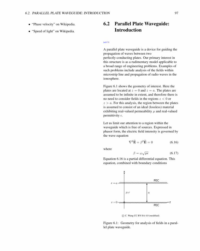
6.2. PARALLEL PLATE WAVEGUIDE: INTRODUCTION 97
• “Phase velocity” on Wikipedia.
• “Speed of light” on Wikipedia.
6.2 Parallel Plate Waveguide:
Introduction
[m0173]
A parallel plate waveguide is a device for guiding the
propagation of waves between two
perfectly-conducting plates. Our primary interest in
this structure is as a rudimentary model applicable to
a broad range of engineering problems. Examples of
such problems include analysis of the fields within
microstrip line and propagation of radio waves in the
ionosphere.
Figure 6.1 shows the geometry of interest. Here the
plates are located at z = 0 and z = a. The plates are
assumed to be infinite in extent, and therefore there is
no need to consider fields in the regions z < 0 or
z > a. For this analysis, the region between the plates
is assumed to consist of an ideal (lossless) material
exhibiting real-valued permeability µ and real-valued
permittivity ǫ.
Let us limit our attention to a region within the
waveguide which is free of sources. Expressed in
phasor form, the electric field intensity is governed by
the wave equation
∇2E+ β2E = 0 (6.16)
where
β = ω√µǫ (6.17)
Equation 6.16 is a partial differential equation. This
equation, combined with boundary conditions
c© C. Wang CC BY-SA 4.0 (modified)
Figure 6.1: Geometry for analysis of fields in a paral-
lel plate waveguide.

98 CHAPTER 6. WAVEGUIDES
imposed by the perfectly-conducting plates, is
sufficient to determine a unique solution. This is most
easily done in Cartesian coordinates, as we shall now
demonstrate. First we express E in Cartesian
coordinates:
E = xEx + yEy + zEz (6.18)
This facilitates the decomposition of Equation 6.16
into separate equations governing the x, y, z
components of E:
∇2Ex + β2Ex = 0 (6.19)
∇2Ey + β2Ey = 0 (6.20)
∇2Ez + β2Ez = 0 (6.21)
Next we observe that the operator ∇2 may be
expressed in Cartesian coordinates as follows:
∇2 =∂2
∂x2+
∂2
∂y2+
∂2
∂z2(6.22)
so the equations governing the Cartesian components
of E may be written as follows:
∂2
∂x2Ex +
∂2
∂y2Ex +
∂2
∂z2Ex = −β2Ex (6.23)
∂2
∂x2Ey +
∂2
∂y2Ey +
∂2
∂z2Ey = −β2Ey (6.24)
∂2
∂x2Ez +
∂2
∂y2Ez +
∂2
∂z2Ez = −β2Ez (6.25)
Let us restrict our attention to scenarios that can be
completely described in two dimensions; namely xand z, and for which there is no variation in y. This is
not necessarily required, however, it is representative
of a broad class of relevant problems, and allows
Equations 6.23–6.25 to be considerably simplified. If
there is no variation in y, then partial derivatives with
respect to y are zero, yielding:
∂2
∂x2Ex +
∂2
∂z2Ex = −β2Ex (6.26)
∂2
∂x2Ey +
∂2
∂z2Ey = −β2Ey (6.27)
∂2
∂x2Ez +
∂2
∂z2Ez = −β2Ez (6.28)
The solution to the parallel plate waveguide problem
may now be summarized as follows: The electric field
E (Equation 6.18) is the solution to simultaneous
Equations 6.26–6.28 subject to the boundary
conditions that apply at the PEC surfaces at z = 0 and
z = d; namely, that the tangent component of E is
zero at these surfaces.
At this point, the problem has been reduced to a
routine exercise in the solution of partial differential
equations. However, a somewhat more useful
approach is to first decompose the total electric field
into transverse electric (TE) and transverse magnetic
(TM) components,2 and determine the solutions to
these components separately. The TE component of
the electric field is parallel to the plates, and therefore
transverse (perpendicular) to the plane shown in
Figure 6.1. Thus, the TE component has
Ex = Ez = 0, and only Ey may be non-zero. The
TM component of the magnetic field intensity (H) is
parallel to the plates, and therefore transverse to the
plane shown in Figure 6.1. Thus, the TM component
has Hx = Hz = 0, and only Hy may be non-zero. As
always, the total field is the sum of the TE and TM
components.
The TE and TM solutions are presented in
Sections 6.3 (Electric component of the TE solution),
6.4 (Magnetic component of the TE solution), and 6.5
(Electric component of the TM solution). The
magnetic component of the TM solution can be
determined via a straightforward variation of the
preceding three cases, and so is not presented here.
Presentation of the solution for the fields in a parallel
plate waveguide under the conditions described in the
section continues in Section 6.3.
2For a refresher on TE-TM decomposition, see Section 5.5.
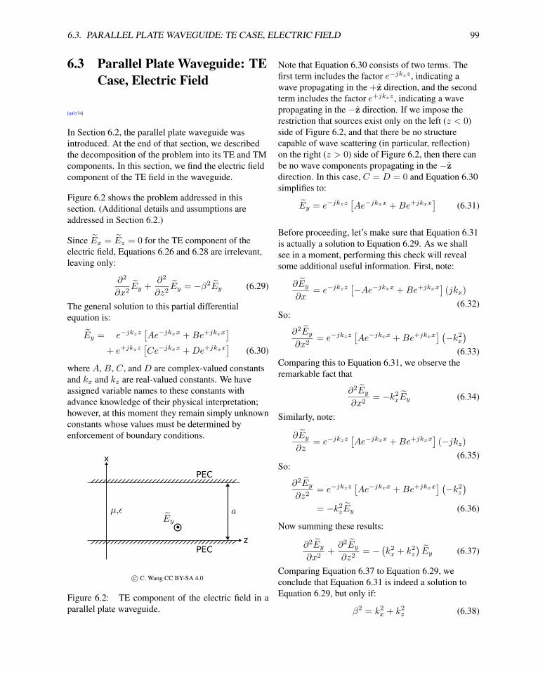
6.3. PARALLEL PLATE WAVEGUIDE: TE CASE, ELECTRIC FIELD 99
6.3 Parallel Plate Waveguide: TE
Case, Electric Field
[m0174]
In Section 6.2, the parallel plate waveguide was
introduced. At the end of that section, we described
the decomposition of the problem into its TE and TM
components. In this section, we find the electric field
component of the TE field in the waveguide.
Figure 6.2 shows the problem addressed in this
section. (Additional details and assumptions are
addressed in Section 6.2.)
Since Ex = Ez = 0 for the TE component of the
electric field, Equations 6.26 and 6.28 are irrelevant,
leaving only:
∂2
∂x2Ey +
∂2
∂z2Ey = −β2Ey (6.29)
The general solution to this partial differential
equation is:
Ey = e−jkzz[Ae−jkxx +Be+jkxx
]
+ e+jkzz[Ce−jkxx +De+jkxx
](6.30)
where A, B, C, and D are complex-valued constants
and kx and kz are real-valued constants. We have
assigned variable names to these constants with
advance knowledge of their physical interpretation;
however, at this moment they remain simply unknown
constants whose values must be determined by
enforcement of boundary conditions.
c© C. Wang CC BY-SA 4.0
Figure 6.2: TE component of the electric field in a
parallel plate waveguide.
Note that Equation 6.30 consists of two terms. The
first term includes the factor e−jkzz , indicating a
wave propagating in the +z direction, and the second
term includes the factor e+jkzz , indicating a wave
propagating in the −z direction. If we impose the
restriction that sources exist only on the left (z < 0)
side of Figure 6.2, and that there be no structure
capable of wave scattering (in particular, reflection)
on the right (z > 0) side of Figure 6.2, then there can
be no wave components propagating in the −z
direction. In this case, C = D = 0 and Equation 6.30
simplifies to:
Ey = e−jkzz[Ae−jkxx +Be+jkxx
](6.31)
Before proceeding, let’s make sure that Equation 6.31
is actually a solution to Equation 6.29. As we shall
see in a moment, performing this check will reveal
some additional useful information. First, note:
∂Ey∂x
= e−jkzz[−Ae−jkxx +Be+jkxx
](jkx)
(6.32)
So:
∂2Ey∂x2
= e−jkzz[Ae−jkxx +Be+jkxx
] (−k2x
)
(6.33)
Comparing this to Equation 6.31, we observe the
remarkable fact that
∂2Ey∂x2
= −k2xEy (6.34)
Similarly, note:
∂Ey∂z
= e−jkzz[Ae−jkxx +Be+jkxx
](−jkz)
(6.35)
So:
∂2Ey∂z2
= e−jkzz[Ae−jkxx +Be+jkxx
] (−k2z
)
= −k2zEy (6.36)
Now summing these results:
∂2Ey∂x2
+∂2Ey∂z2
= −(k2x + k2z
)Ey (6.37)
Comparing Equation 6.37 to Equation 6.29, we
conclude that Equation 6.31 is indeed a solution to
Equation 6.29, but only if:
β2 = k2x + k2z (6.38)

100 CHAPTER 6. WAVEGUIDES
This confirms that kx and kz are in fact the
components of the propagation vector
k , βk = xkx + yky + zkz (6.39)
where k is the unit vector pointing in the direction of
propagation, and ky = 0 in this particular problem.
The solution has now been reduced to finding the
constants A, B, and either kx or kz . This is
accomplished by enforcing the relevant boundary
conditions. In general, the component of E that is
tangent to a perfectly-conducting surface is zero.
Applied to the present problem, this means Ey = 0 at
x = 0 and Ey = 0 at x = a. Referring to
Equation 6.31, the boundary condition at x = 0means
e−jkzz [A · 1 +B · 1] = 0 (6.40)
The factor e−jkzz cannot be zero; therefore,
A+B = 0. Since B = −A, we may rewrite
Equation 6.31 as follows:
Ey = e−jkzzB[e+jkxx − e−jkxx
](6.41)
This expression is simplified using a trigonometric
identity:
1
2j
[e+jkxx − e−jkxx
]= sin kxx (6.42)
Let us now make the definition Ey0 , j2B. Then:
Ey = Ey0e−jkzz sin kxx (6.43)
Now applying the boundary condition at x = a:
Ey0e−jkzz sin kxa = 0 (6.44)
The factor e−jkzz cannot be zero, and Ey0 = 0 yields
only trivial solutions; therefore:
sin kxa = 0 (6.45)
This in turn requires that
kxa = mπ (6.46)
where m is an integer. Note that m = 0 is not of
interest since this yields kx = 0, which according to
Equation 6.43 yields the trivial solution Ey = 0. Also
each integer value of m that is less than zero is
excluded because the associated solution is different
from the solution for the corresponding positive value
of m in sign only, which can be absorbed in the
arbitrary constant Ey0.
At this point we have uncovered a family of solutions
given by Equation 6.43 and Equation 6.46 with
m = 1, 2, .... Each solution associated with a
particular value of m is referred to as a mode, which
(via Equation 6.46) has a particular value of kx. The
value of kz for mode m is obtained using
Equation 6.38 as follows:
kz =√β2 − k2x
=
√β2 −
(mπa
)2(6.47)
Since kz is specified to be real-valued, we require:
β2 −(mπa
)2> 0 (6.48)
This constrains β; specifically:
β >mπ
a(6.49)
Recall that β = ω√µǫ and ω = 2πf where f is
frequency. Solving for f , we find:
f >m
2a√µǫ
(6.50)
Therefore, each mode exists only above a certain
frequency, which is different for each mode. This
cutoff frequency fc for mode m is given by
f (m)c ,
m
2a√µǫ
(6.51)
At frequencies below the cutoff frequency for mode
m, modes 1 through m− 1 exhibit imaginary-valued
kz . The propagation constant must have a real-valued
component in order to propagate; therefore, these
modes do not propagate and may be ignored.
Let us now summarize the solution. For the scenario
depicted in Figure 6.2, the electric field component of
the TE solution is given by:
yEy = y
∞∑
m=1
E(m)y (6.52)

6.3. PARALLEL PLATE WAVEGUIDE: TE CASE, ELECTRIC FIELD 101
where
E(m)y ,
0, f < f
(m)c
E(m)y0 e−jk
(m)z z sin k
(m)x x, f ≥ f
(m)c
(6.53)
where m enumerates modes (m = 1, 2, ...),
k(m)z ,
√β2 −
[k(m)x
]2(6.54)
and
k(m)x , mπ/a (6.55)
Finally, E(m)y0 is a complex-valued constant that
depends on sources or boundary conditions to the left
of the region of interest.
For the scenario depicted in Figure 6.2, the elec-
tric field component of the TE solution is given
by Equation 6.52 with modal components deter-
mined as indicated by Equations 6.51–6.55. This
solution presumes all sources lie to the left of the
region of interest, and no scattering occurs to the
right of the region of interest.
To better understand this result, let us examine the
lowest-order mode, m = 1. For this mode
f(1)c = 1/2a
√µǫ, so this mode can exist if
f > 1/2a√µǫ. Also k
(1)x = π/a, so
k(1)z =
√β2 −
(πa
)2(6.56)
Subsequently,
E(1)y = E
(1)y0 e
−jk(1)z z sinπx
a(6.57)
Note that this mode has the form of a plane wave. The
plane wave propagates in the +z direction with phase
propagation constant k(1)z . Also, we observe that the
apparent plane wave is non-uniform, exhibiting
magnitude proportional to sinπx/a within the
waveguide. This is shown in Figure 6.3 (left image).
In particular, we observe that the magnitude of the
wave is zero at the perfectly-conducting surfaces – as
is necessary to satisfy the boundary conditions – and
is maximum in the center of the waveguide.
Now let us examine the m = 2 mode. For this mode,
f(2)c = 1/a
√µǫ, so this mode can exist if
c© C. Wang CC BY-SA 4.0
Figure 6.3: Magnitude of the two lowest-order TE
modes in a parallel plate waveguide. Left: m = 1,
Right: m = 2.
f > 1/a√µǫ. This frequency is higher than f
(1)c , so
the m = 1 mode can exist at any frequency at which
the m = 2 mode exists. Also k(2)x = 2π/a, so
k(2)z =
√
β2 −(2π
a
)2
(6.58)
Subsequently,
E(2)y = E
(2)y0 e
−jk(2)z z sin2πx
a(6.59)
In this case, the apparent plane wave propagates in the
+z direction with phase propagation constant k(2)z ,
which is less than k(1)z . For m = 2, we find
magnitude is proportional to sin 2πx/a within the
waveguide (Figure 6.3, right image). As in the m = 1case, we observe that the magnitude of the wave is
zero at the PEC surfaces; however, for m = 2, there
are two maxima with respect to x, and the magnitude
in the center of the waveguide is zero.
This pattern continues for higher-order modes. In
particular, each successive mode exhibits higher
cutoff frequency, smaller propagation constant, and
increasing integer number of sinusoidal half-periods
in magnitude.
Example 6.2. Single-mode TE propagation in a
parallel plate waveguide.
Consider an air-filled parallel plate waveguide
consisting of plates separated by 1 cm.
Determine the frequency range for which one

102 CHAPTER 6. WAVEGUIDES
(and only one) propagating TE mode is assured.
Solution. Single-mode TE propagation is
assured by limiting frequency f to greater than
the cutoff frequency for m = 1, but lower than
the cutoff frequency for m = 2. (Any frequency
higher than the cutoff frequency for m = 2allows at least 2 modes to exist.) Calculating the
applicable cutoff frequencies, we find:
f (1)c =1
2a√µ0ǫ0
∼= 15.0 GHz (6.60)
f (2)c =2
2a√µ0ǫ0
∼= 30.0 GHz (6.61)
Therefore, 15.0 GHz ≤ f ≤ 30.0 GHz.
Finally, let us consider the phase velocity vp within
the waveguide. For lowest-order mode m = 1, this is
vp =ω
k(1)z
=ω√
ω2µǫ−(πa
)2 (6.62)
Recall that the speed of an electromagnetic wave in
unbounded space (i.e., not in a waveguide) is 1/√µǫ.
For example, the speed of light in free space is
1/√µ0ǫ0 = c. However, the phase velocity indicated
by Equation 6.62 is greater than 1/√µǫ; e.g., faster
than light would travel in the same material
(presuming it were transparent). At first glance, this
may seem to be impossible. However, recall that
information travels at the group velocity vg, and not
necessarily the phase velocity. (See Section 6.1 for a
refresher.) Although we shall not demonstrate this
here, the group velocity in the parallel plate
waveguide is always less than 1/√µǫ, so no physical
laws are broken, and signals travel somewhat slower
than the speed of light, as they do in any other
structure used to convey signals.
Also remarkable is that the speed of propagation is
different for each mode. In fact, we find that the phase
velocity increases and the group velocity decreases as
m increases. This phenomenon is known as
dispersion, and sometimes specifically as mode
dispersion or modal dispersion.
6.4 Parallel Plate Waveguide: TE
Case, Magnetic Field
[m0175]
In Section 6.2, the parallel plate waveguide was
introduced. In Section 6.3, we determined the TE
component of the electric field. In this section, we
determine the TE component of the magnetic field.
The reader should be familiar with Section 6.3 before
attempting this section.
In Section 6.3, the TE component of the electric field
was determined to be:
yEy = y
∞∑
m=1
E(m)y (6.63)
The TE component of the magnetic field may be
obtained from the Maxwell-Faraday equation:
∇× E = −jωµH (6.64)
Thus:
H =j
ωµ∇× E
=j
ωµ∇×
(yEy
)(6.65)
The relevant form of the curl operator is
Equation B.16 (Appendix B.2). Although the
complete expression consists of 6 terms, all but 2 of
these terms are zero because the x and z components
of E are zero. The two remaining terms are
−x∂Ey/∂z and +z∂Ey/∂x. Thus:
H =j
ωµ
(−x
∂Ey∂z
+ z∂Ey∂x
)(6.66)
Recall that Ey is the sum of modes, as indicated in
Equation 6.63. Since differentiation (i.e., ∂/∂z and
∂/∂x) is a linear operator, we may evaluate
Equation 6.66 for modes one at a time, and then sum
the results. Using this approach, we find:
∂E(m)y
∂z=
∂
∂zE
(m)y0 e−jk
(m)z z sin k(m)
x x
=(E
(m)y0 e−jk
(m)z z sin k(m)
x x)(
−jk(m)z
)
(6.67)

6.4. PARALLEL PLATE WAVEGUIDE: TE CASE, MAGNETIC FIELD 103
and
∂E(m)y
∂x=
∂
∂xE
(m)y0 e−jk
(m)z z sin k(m)
x x
=(E
(m)y0 e−jk
(m)z z cos k(m)
x x)(
+k(m)x
)
(6.68)
We may now assemble a solution for the magnetic
field as follows:
xHx + zHz = x
∞∑
m=1
H(m)x
+ z
∞∑
m=1
H(m)z (6.69)
where
H(m)x = −k
(m)z
ωµE
(m)y0 e−jk
(m)z z sin k(m)
x x (6.70)
H(m)z = +j
k(m)x
ωµE
(m)y0 e−jk
(m)z z cos k(m)
x x (6.71)
and modes may only exist at frequencies greater than
the associated cutoff frequencies. Summarizing:
The magnetic field component of the TE solu-
tion is given by Equation 6.69 with modal com-
ponents as indicated by Equations 6.70 and 6.71.
Caveats pertaining to the cutoff frequencies and
the locations of sources and structures continue
to apply.
This result is quite complex, yet some additional
insight is possible. At the perfectly-conducting (PEC)
surface at x = 0, we see
H(m)x (x = 0) = 0
H(m)z (x = 0) = +j
k(m)x
ωµE
(m)y0 e−jk
(m)z z (6.72)
Similarly, on the PEC surface at x = a, we see
H(m)x (x = a) = 0
H(m)z (x = a) = −j k
(m)x
ωµE
(m)y0 e−jk
(m)z z (6.73)
Thus, we see the magnetic field vector at the PEC
surfaces is non-zero and parallel to the PEC surfaces.
Recall that the magnetic field is identically zero inside
a PEC material. Also recall that boundary conditions
require that discontinuity in the component of H
tangent to a surface must be supported by a surface
current. We conclude that
Current flows on the PEC surfaces of the waveg-
uide.
If this seems surprising, note that essentially the same
thing happens in a coaxial transmission line. That is,
signals in a coaxial transmission line can be described
equally well in terms of either potentials and currents
on the inner and outer conductors, or the
electromagnetic fields between the conductors. The
parallel plate waveguide is only slightly more
complicated because the field in a properly-designed
coaxial cable is a single transverse electromagnetic
(TEM) mode, whereas the fields in a parallel plate
waveguide are combinations of TE and TM modes.
Interestingly, we also find that the magnetic field
vector points in different directions depending on
position relative to the conducting surfaces. We just
determined that the magnetic field is parallel to the
conducting surfaces at those surfaces. However, the
magnetic field is perpendicular to those surfaces at mlocations between x = 0 and x = a. These locations
correspond to maxima in the electric field.

104 CHAPTER 6. WAVEGUIDES
6.5 Parallel Plate Waveguide:
TM Case, Electric Field
[m0177]
In Section 6.2, the parallel plate waveguide shown in
Figure 6.4 was introduced. At the end of that section,
we decomposed the problem into its TE and TM
components. In this section, we find the TM
component of the fields in the waveguide.
“Transverse magnetic” means the magnetic field
vector is perpendicular to the plane of interest, and is
therefore parallel to the conducting surfaces. Thus,
H = yHy , with no component in the x or z
directions. Following precisely the same reasoning
employed in Section 6.2, we find the governing
equation for the magnetic component of TM field is:
∂2
∂x2Hy +
∂2
∂z2Hy = −β2Hy (6.74)
The general solution to this partial differential
equation is:
Hy = e−jkzz[Ae−jkxx +Be+jkxx
]
+ e+jkzz[Ce−jkxx +De+jkxx
](6.75)
where A, B, C, and D are complex-valued constants;
and kx and kz are real-valued constants. We have
assigned variable names to these constants with
advance knowledge of their physical interpretation;
however, at this moment they remain simply unknown
constants whose values must be determined by
enforcement of boundary conditions.
c© C. Wang CC BY-SA 4.0
Figure 6.4: TM component of the electric field in a
parallel plate waveguide.
Note that Equation 6.75 consists of two terms. The
first term includes the factor e−jkzz , indicating a
wave propagating in the +z direction, and the second
term includes the factor e+jkzz , indicating a wave
propagating in the −z direction. If we impose the
restriction that sources exist only on the left (z < 0)
side of Figure 6.4, and that there be no structure
capable of wave scattering (in particular, reflection)
on the right (z > 0) side of Figure 6.4, then there can
be no wave components propagating in the −z
direction. In this case, C = D = 0 and Equation 6.75
simplifies to:
Hy = e−jkzz[Ae−jkxx +Be+jkxx
](6.76)
Before proceeding, let’s make sure that Equation 6.76
is actually a solution to Equation 6.74. As in the TE
case, this check yields a constraint (in fact, the same
constraint) on the as-yet undetermined parameters kxand kz . First, note:
∂Hy
∂x= e−jkzz
[−Ae−jkxx +Be+jkxx
](jkx)
(6.77)
So:
∂2Hy
∂x2= e−jkzz
[Ae−jkxx +Be+jkxx
] (−k2x
)
= −k2xHy (6.78)
Next, note:
∂Hy
∂z= e−jkzz
[Ae−jkxx +Be+jkxx
](−jkz)
(6.79)
So:
∂2Hy
∂z2= e−jkzz
[Ae−jkxx +Be+jkxx
] (−k2z
)
= −k2zHy (6.80)
Now summing these results:
∂2Hy
∂x2+∂2Hy
∂z2= −
(k2x + k2z
)Hy (6.81)
Comparing Equation 6.81 to Equation 6.74, we
conclude that Equation 6.76 is a solution to
Equation 6.74 under the constraint that:
β2 = k2x + k2z (6.82)
6.5. PARALLEL PLATE WAVEGUIDE: TM CASE, ELECTRIC FIELD 105
This is precisely the same constraint identified in the
TE case, and confirms that kx and ky are in fact the
components of the propagation vector
k , βk = xkx + yky + zkz (6.83)
where k is the unit vector pointing in the direction of
propagation, and ky = 0 in this particular problem.
Our objective in this section is to determine the
electric field component of the TM field. The electric
field may be obtained from the magnetic field using
Ampere’s law:
∇× H = jωǫE (6.84)
Thus:
E =1
jωǫ∇× H
=1
jωǫ∇×
(yHy
)(6.85)
The relevant form of the curl operator is
Equation B.16 (Appendix B.2). Although the
complete expression consists of 6 terms, all but 2 of
these terms are zero because the x and z components
of H are zero. The two remaining terms are
−x∂Hy/∂z and +z∂Hy/∂x. Thus:
E =1
jωǫ
(−x
∂Hy
∂z+ z
∂Hy
∂x
)(6.86)
We may further develop this expression using
Equations 6.77 and 6.79. We find the x component of
E is:
Ex =kzωǫ
e−jkzz[Ae−jkxx +Be+jkxx
](6.87)
and the z component of E is:
Ez =kxωǫ
e−jkzz[−Ae−jkxx +Be+jkxx
](6.88)
The solution has now been reduced to the problem of
finding the constants A, B, and either kx or kz . This
is accomplished by enforcing the relevant boundary
conditions. In general, the component of the electric
field which is tangent to a perfectly-conducting
surface is zero. Applied to the present (TM) case, this
means Ez (x = 0) = 0 and Ez (x = a) = 0.
Referring to Equation 6.88, the boundary condition at
x = 0 means
kxωǫ
e−jkzz [−A (1) +B (1)] = 0 (6.89)
The factor e−jkzz always has unit magnitude, and so
cannot be zero. We could require kx to be zero, but
this is unnecessarily restrictive. Instead, we require
A = B and we may rewrite Equation 6.88 as follows:
Ez =Bkxωǫ
e−jkzz[e+jkxx − e−jkxx
](6.90)
This expression is simplified using a trigonometric
identity:
sin kxa =1
2j
[e+jkxa − e−jkxa
](6.91)
Thus:
Ez =j2Bkxωǫ
e−jkzz sin kxx (6.92)
Now following up with Ex, beginning from
Equation 6.87:
Ex =kzωǫ
e−jkzz[Ae−jkxx +Be+jkxx
]
=Bkzωǫ
e−jkzz[e−jkxx + e+jkxx
]
=2Bkzωǫ
e−jkzz cos kxx (6.93)
For convenience we define the following
complex-valued constant:
Ex0 ,2Bkzωǫ
(6.94)
This yields the following simpler expression:
Ex = Ex0 e−jkzz cos kxx (6.95)
Now let us apply the boundary condition at x = a to
Ez:j2Bkzωǫ
e−jkzz sin kxa = 0 (6.96)
Requiring B = 0 or kz = 0 yields only trivial
solutions, therefore, it must be true that
sin kxa = 0 (6.97)
This in turn requires that
kxa = mπ (6.98)

106 CHAPTER 6. WAVEGUIDES
where m is an integer. Note that this is precisely the
same relationship that we identified in the TE case.
There is an important difference, however. In the TE
case, m = 0 was not of interest because this yields
kx = 0, and the associated field turned out to be
identically zero. In the present (TM) case, m = 0 also
yields kx = 0, but the associated field is not
necessarily zero. That is, for m = 0, Ez = 0 but Exis not necessarily zero. Therefore, m = 0 as well as
m = 1, m = 2, and so on are of interest in the TM
case.
At this point, we have uncovered a family of solutions
with m = 0, 1, 2, .... Each solution is referred to as a
mode, and is associated with a particular value of kx.
In the discussion that follows, we shall find that the
consequences are identical to those identified in the
TE case, except that m = 0 is now also allowed.
Continuing: The value of kz for mode m is obtained
using Equation 6.82 as follows:
kz =√β2 − k2x
=
√β2 −
(mπa
)2(6.99)
Since kz is specified to be real-valued, we require:
β2 −(mπa
)2> 0 (6.100)
This constrains β; specifically:
β >mπ
a(6.101)
Recall that β = ω√µǫ and ω = 2πf where f is
frequency. Solving for f , we find:
f >m
2a√µǫ
(6.102)
Thus, each mode exists only above a certain
frequency, which is different for each mode. This
cutoff frequency fc for mode m is given by
f (m)c ,
m
2a√µǫ
(6.103)
At frequencies below the cutoff frequency for mode
m, modes 0 through m− 1 exhibit imaginary-valued
kz and therefore do no propagate. Also, note that the
cutoff frequency for m = 0 is zero, and so this mode
is always able to propagate. That is, the m = 0 mode
may exist for any a > 0 and any f > 0. Once again,
this is a remarkable difference from the TE case, for
which m = 0 is not available.
Let us now summarize the solution. With respect to
Figure 6.4, we find that the electric field component
of the TM field is given by:
E =
∞∑
m=0
[xE(m)
x + zE(m)z
](6.104)
where
E(m)x ,
0, f < f
(m)c
E(m)x0 e−jk
(m)z z cos k
(m)x x, f ≥ f
(m)c
(6.105)
and
E(m)z ,
0, f < f
(m)c
jk(m)x
k(m)z
E(m)x0 e−jk
(m)z z sin k
(m)x x, f ≥ f
(m)c
(6.106)
where m enumerates modes (m = 0, 1, 2, ...) and
k(m)z ,
√β2 −
[k(m)x
]2(6.107)
k(m)x , mπ/a (6.108)
Finally, the coefficients E(m)x0 depend on sources
and/or boundary conditions to the left of the region of
interest.
For the scenario depicted in Figure 6.4, the elec-
tric field component of the TM solution is given
by Equation 6.104 with modal components de-
termined as indicated by Equations 6.103–6.108.
This solution presumes all sources lie to the
left of the region of interest, with no additional
sources or boundary conditions to the right of the
region of interest.
The m = 0 mode, commonly referred to as the
“TM0” mode, is of particular importance in the
analysis of microstrip transmission line, and is
addressed in Section 6.6.

6.6. PARALLEL PLATE WAVEGUIDE: THE TM0 MODE 107
6.6 Parallel Plate Waveguide:
The TM0 Mode
[m0220]
In Section 6.2, the parallel plate waveguide (also
shown in Figure 6.5) was introduced. At the end of
that section we decomposed the problem into its
constituent TE and TM fields. In Section 6.5, we
determined the electric field component of the TM
field, which was found to consist of a set of discrete
modes. In this section, we address the lowest-order
(m = 0) mode of the TM field, which has special
relevance in a number of applications including
microstrip transmission lines. This mode is
commonly referred to as the “TM0” mode.
The TM electric field intensity in the waveguide is
given by Equation 6.104 with modal components
determined as indicated by Equations 6.103–6.108
(Section 6.5). Recall that the m = 0 mode can only
exist only in the TM case, and does not exist in the
TE case. We also noted that the cutoff frequency for
this mode is zero, so it may exist at any frequency,
and within any non-zero plate separation a. For this
mode k(0)x = 0, k
(0)z = β, and we find
E = xE(0)x0 e
−jβz (TM0 mode) (6.109)
Remarkably, we find that this mode has the form of a
uniform plane wave which propagates in the +z
direction; i.e., squarely between the plates. The phase
and group velocities of this wave are equal to each
other and ω/β, precisely as expected for a uniform
c© C. Wang CC BY-SA 4.0 (modified)
Figure 6.5: TM0 mode in a parallel plate waveguide.
plane wave in unbounded media; i.e., as if the plates
did not exist. This observation allows us to easily
determine the associated magnetic field: Using the
plane wave relationship,
H =1
ηk× E (6.110)
=1
ηz×
(xE
(0)x0 e
−jβz)
(6.111)
= yE
(0)x0
ηe−jβz (TM0 mode) (6.112)
Example 6.3. Guided waves in a printed circuit
board (PCB).
A very common form of PCB consists of a
1.575 mm-thick slab of low-loss dielectric
having relative permittivity ≈ 4.5 sandwiched
between two copper planes. Characterize the
electromagnetic field in a long strip of this
material. Assume a single source exists at one
end of the strip, and operates at frequencies
below 10 GHz.
Solution. Let us assume that the copper planes
exhibit conductivity that is sufficiently high that
the inward-facing surfaces may be viewed as
perfectly-conducting. Also, let us limit scope to
the field deep within the “sandwich,” and neglect
the region near the edges of the PCB. Under
these conditions, the PCB is well-modeled as a
parallel-plate waveguide. Thus, the
electromagnetic field consists of a combination
of TE and TM modes. The active (non-zero)
modes depend on the source (a mode must be
“stimulated” by the source in order to propagate)
and modal cutoff frequencies. The cutoff
frequency for mode m is
f (m)c =
m
2a√µǫ
(6.113)
In this case, a = 1.575 mm, µ ≈ µ0, and
ǫ ≈ 4.5ǫ0. Therefore:
f (m)c ≈ (44.9 GHz)m (6.114)
Since the cutoff frequency for m = 1 is much
greater than 10 GHz, we may rest assured that

108 CHAPTER 6. WAVEGUIDES
the only mode that can propagate inside the PCB
is TM0. Therefore, the field deep inside the PCB
may be interpreted as a single plane wave having
the TM0 structure shown in Figure 6.5,
propagating away from the source end of the
PCB. The phase velocity is simply that of the
apparent plane wave:
vp =1√µǫ
≈ 1.41× 10⁸ m/s ≈ 0.47c (6.115)
The scenario described in this example is essentially a
very rudimentary form of microstrip transmission
line.
6.7 General Relationships for
Unidirectional Waves
[m0222]
Analysis of electromagnetic waves in enclosed spaces
– and in waveguides in particular – is quite difficult.
The task is dramatically simplified if it can be
assumed that the wave propagates in a single
direction; i.e., is unidirectional. This does not
necessarily entail loss of generality. For example:
Within a straight waveguide, waves can travel either
“forward” or “backward.” The principle of
superposition allows one to consider these two
unidirectional cases separately, and then to simply
sum the results.
In this section, the equations that relate the various
components of a unidirectional wave are derived. The
equations will be derived in Cartesian coordinates,
anticipating application to rectangular waveguides.
However, the underlying strategy is generally
applicable.
We begin with Maxwell’s curl equations:
∇× E = −jωµH (6.116)
∇× H = +jωǫE (6.117)
Let us consider Equation 6.117 first. Solving for E,
we have:
E =1
jωǫ∇× H (6.118)
This is actually three equations; that is, one each for
the x, y, and z components of E, respectively. To
extract these equations, let us define the components
as follows:
E = xEx + yEy + zEz (6.119)
H = xHx + yHy + zHz (6.120)
Now applying the equation for curl in Cartesian
coordinates (Equation B.16 in Appendix B.2), we

6.7. GENERAL RELATIONSHIPS FOR UNIDIRECTIONAL WAVES 109
find:
Ex =1
jωǫ
(∂Hz
∂y− ∂Hy
∂z
)(6.121)
Ey =1
jωǫ
(∂Hx
∂z− ∂Hz
∂x
)(6.122)
Ez =1
jωǫ
(∂Hy
∂x− ∂Hx
∂y
)(6.123)
Without loss of generality, we may assume that the
single direction in which the wave is traveling is in
the +z direction. If this is the case, then H, and
subsequently each component of H, contains a factor
of e−jkzz where kz is the phase propagation constant
in the direction of travel. The remaining factors are
independent of z; i.e., depend only on x and y. With
this in mind, we further decompose components of H
as follows:
Hx = hx(x, y)e−jkzz (6.124)
Hy = hy(x, y)e−jkzz (6.125)
Hz = hz(x, y)e−jkzz (6.126)
where hx(x, y), hy(x, y), and hz(x, y) represent the
remaining factors. One advantage of this
decomposition is that partial derivatives with respect
to z reduce to algebraic operations; i.e.:
∂Hx
∂z= −jkzhx(x, y)e−jkzz = −jkzHx (6.127)
∂Hy
∂z= −jkzhy(x, y)e−jkzz = −jkzHy (6.128)
∂Hz
∂z= −jkzhz(x, y)e−jkzz = −jkzHz (6.129)
We now substitute Equations 6.124–6.126 into
Equations 6.121–6.123 and then use
Equations 6.127–6.129 to eliminate partial derivatives
with respect to z. This yields:
Ex =1
jωǫ
(∂Hz
∂y+ jkzHy
)(6.130)
Ey =1
jωǫ
(−jkzHx −
∂Hz
∂x
)(6.131)
Ez =1
jωǫ
(∂Hy
∂x− ∂Hx
∂y
)(6.132)
Applying the same procedure to the curl equation for
H (Equation 6.116), one obtains:
Hx =1
−jωµ
(∂Ez∂y
+ jkzEy
)(6.133)
Hy =1
−jωµ
(−jkzEx −
∂Ez∂x
)(6.134)
Hz =1
−jωµ
(∂Ey∂x
− ∂Ex∂y
)(6.135)
Equations 6.130–6.135 constitute a set of
simultaneous equations that represent Maxwell’s curl
equations in the special case of a unidirectional
(specifically, a +z-traveling) wave. With just a little
bit of algebraic manipulation of these equations, it is
possible to obtain expressions for the x and y
components of E and H which depend only on the z
components of E and H. Here they are:3
Ex =−jk2ρ
(+kz
∂Ez∂x
+ ωµ∂Hz
∂y
)(6.136)
Ey =+j
k2ρ
(−kz
∂Ez∂y
+ ωµ∂Hz
∂x
)(6.137)
Hx =+j
k2ρ
(ωǫ∂Ez∂y
− kz∂Hz
∂x
)(6.138)
Hy =−jk2ρ
(ωǫ∂Ez∂x
+ kz∂Hz
∂y
)(6.139)
where
k2ρ , β2 − k2z (6.140)
Why define a parameter called “kρ”? Note from the
definition that β2 = k2ρ + k2z . Further, note that this
equation is an expression of the Pythagorean theorem,
which relates the lengths of the sides of a right
triangle. Since β is the “overall” phase propagation
constant, and kz is the phase propagation constant for
propagation in the z direction in the waveguide, kρmust be associated with variation in fields in
directions perpendicular to z. In the cylindrical
coordinate system, this is the ρ direction, hence the
subscript “ρ.” We shall see later that kρ plays a special
3Students are encouraged to derive these for themselves – only
algebra is required. Tip to get started: To get Ex, begin with Equa-
tion 6.130, eliminate Hy using Equation 6.134, and then solve for
Ex.

110 CHAPTER 6. WAVEGUIDES
role in determining the structure of fields within the
waveguide, and this provides additional motivation to
identify this quantity explicitly in the field equations.
Summarizing: If you know the wave is unidirectional,
then knowledge of the components of E and H in the
direction of propagation is sufficient to determine
each of the remaining components of E and H. There
is one catch, however: For this to yield sensible
results, kρ may not be zero. So, ironically, these
expressions don’t work in the case of a uniform plane
wave, since such a wave would have Ez = Hz = 0and kz = β (so kρ = 0), yielding values of zero
divided by zero for each remaining field component.
The same issue arises for any other transverse
electromagnetic (TEM) wave. For non-TEM waves –
and, in particular, unidirectional waves in waveguides
– either Ez or Hz must be non-zero and kρ will be
non-zero. In this case, Equations 6.136–6.139 are
both usable and useful since they allow determination
of all field components given just the z components.
In fact, we may further exploit this simplicity by
taking one additional step: Decomposition of the
unidirectional wave into transverse electric (TE) and
transverse magnetic (TM) components. In this case,
TE means simply that Ez = 0, and TM means simply
that Hz = 0. For a wave which is either TE or TM,
Equations 6.136–6.139 reduce to one term each.
6.8 Rectangular Waveguide: TM
Modes
[m0223]
A rectangular waveguide is a conducting cylinder of
rectangular cross section used to guide the
propagation of waves. Rectangular waveguide is
commonly used for the transport of radio frequency
signals at frequencies in the SHF band (3–30 GHz)
and higher. The fields in a rectangular waveguide
consist of a number of propagating modes which
depends on the electrical dimensions of the
waveguide. These modes are broadly classified as
either transverse magnetic (TM) or transverse electric
(TE). In this section, we consider the TM modes.
Figure 6.6 shows the geometry of interest. Here the
walls are located at x = 0, x = a, y = 0, and y = b;thus, the cross-sectional dimensions of the waveguide
are a and b. The interior of the waveguide is presumed
to consist of a lossless material exhibiting real-valued
permeability µ and real-valued permittivity ǫ, and the
walls are assumed to be perfectly-conducting.
Let us limit our attention to a region within the
waveguide which is free of sources. Expressed in
phasor form, the electric field intensity within the
waveguide is governed by the wave equation
∇2E+ β2E = 0 (6.141)
where
β = ω√µǫ (6.142)
Figure 6.6: Geometry for analysis of fields in a rect-
angular waveguide.

6.8. RECTANGULAR WAVEGUIDE: TM MODES 111
Equation 6.141 is a partial differential equation. This
equation, combined with boundary conditions
imposed by the perfectly-conducting plates, is
sufficient to determine a unique solution. This
solution is most easily determined in Cartesian
coordinates, as we shall now demonstrate. First we
express E in Cartesian coordinates:
E = xEx + yEy + zEz (6.143)
This facilitates the decomposition of Equation 6.141
into separate equations governing the x, y, and z
components of E:
∇2Ex + β2Ex = 0 (6.144)
∇2Ey + β2Ey = 0 (6.145)
∇2Ez + β2Ez = 0 (6.146)
Next we observe that the operator ∇2 may be
expressed in Cartesian coordinates as follows:
∇2 =∂2
∂x2+
∂2
∂y2+
∂2
∂z2(6.147)
so the equations governing the Cartesian components
of E may be written as follows:
∂2
∂x2Ex +
∂2
∂y2Ex +
∂2
∂z2Ex + β2Ex = 0 (6.148)
∂2
∂x2Ey +
∂2
∂y2Ey +
∂2
∂z2Ey + β2Ey = 0 (6.149)
∂2
∂x2Ez +
∂2
∂y2Ez +
∂2
∂z2Ez + β2Ez = 0 (6.150)
In general, we expect the total field in the waveguide
to consist of unidirectional waves propagating in the
+z and −z directions. We may analyze either of
these waves; then the other wave is easily derived via
symmetry, and the total field is simply a linear
combination (superposition) of these waves. With this
in mind, we limit our focus to the wave propagating
in the +z direction.
In Section 6.7, it is shown that all components of the
electric and magnetic fields can be easily calculated
once Ez and Hz are known. The problem is further
simplified by decomposing the unidirectional wave
into TM and TE components. In this decomposition,
the TM component is defined by the property that
Hz = 0; i.e., is transverse (perpendicular) to the
direction of propagation. Thus, the TM component is
completely determined by Ez .
Equations 6.136–6.139 simplify to become:
Ex = −j kzk2ρ
∂Ez∂x
(6.151)
Ey = −j kzk2ρ
∂Ez∂y
(6.152)
Hx = +jωµ
k2ρ
∂Ez∂y
(6.153)
Hy = −j ωµk2ρ
∂Ez∂x
(6.154)
where
k2ρ , β2 − k2z (6.155)
and kz is the phase propagation constant; i.e., the
wave is assumed to propagate according to e−jkzz .
Now let us address the problem of finding Ez , which
will then completely determine the TM field. As in
Section 6.7, we recognize that Ez can be represented
as the propagation factor e−jkzz times a factor that
describes variation with respect to the remaining
spatial dimensions x and y:
Ez = ez(x, y)e−jkzz (6.156)
Substitution of this expression into Equation 6.150
and dividing out the common factor of e−jkzz yields:
∂2
∂x2ez +
∂2
∂y2ez − k2z ez + β2ez = 0 (6.157)
The last two terms may be combined using
Equation 6.155, yielding:
∂2
∂x2ez +
∂2
∂y2ez + k2ρez = 0 (6.158)
This is a partial differential equation for ez in the
variables x and y. This equation may be solved using
the technique of separation of variables. In this
technique, we recognize that ez(x, y) can be written
as the product of a function X(x) which depends only
on x, and a function Y (y) that depends only on y.
That is,
ez(x, y) = X(x)Y (y) (6.159)

112 CHAPTER 6. WAVEGUIDES
Substituting this expression into Equation 6.158, we
obtain:
Y∂2
∂x2X +X
∂2
∂y2Y + k2ρXY = 0 (6.160)
Next dividing through by XY , we obtain:
1
X
∂2
∂x2X +
1
Y
∂2
∂y2Y + k2ρ = 0 (6.161)
Note that the first term depends only on x, the second
term depends only on y, and the remaining term is a
constant. Therefore, the sum of the first and second
terms is a constant; namely −k2ρ. Since these terms
depend on either x or y, and not both, the first term
must equal some constant, the second term must
equal some constant, and these constants must sum to
−k2ρ. Therefore, we are justified in separating the
equation into two equations as follows:
1
X
∂2
∂x2X + k2x = 0 (6.162)
1
Y
∂2
∂y2Y + k2y = 0 (6.163)
where the new constants k2x and k2y must satisfy
k2x + k2y = k2ρ (6.164)
Now multiplying Equations 6.162 and 6.163 by Xand Y , respectively, we find:
∂2
∂x2X + k2xX = 0 (6.165)
∂2
∂y2Y + k2yY = 0 (6.166)
These are familiar one-dimensional differential
equations. The solutions are:4
X = A cos (kxx) +B sin (kxx) (6.167)
Y = C cos (kyy) +D sin (kyy) (6.168)
where A, B, C, and D – like kx and ky – are
constants to be determined. At this point, we observe
that the wave we seek can be expressed as follows:
Ez = ez(x, y)e−jkzz
= X(x) Y (y) e−jkzz (6.169)
4Students are encouraged to confirm that these are correct by
confirming that they are solutions to Equations 6.165 and 6.165, re-
spectively.
The solution is essentially complete except for the
values of the constants A, B, C, D, kx, and ky . The
values of these constants are determined by applying
the relevant electromagnetic boundary condition. In
this case, it is required that the component of E that is
tangent to a perfectly-conducting wall must be zero.
Note that the z component of E is tangent to all four
walls; therefore:
Ez (x = 0) = 0 (6.170)
Ez (x = a) = 0 (6.171)
Ez (y = 0) = 0 (6.172)
Ez (y = b) = 0 (6.173)
Referring to Equation 6.169, these boundary
conditions in turn require:
X (x = 0) = 0 (6.174)
X (x = a) = 0 (6.175)
Y (y = 0) = 0 (6.176)
Y (y = b) = 0 (6.177)
Evaluating these conditions using Equations 6.167
and 6.168 yields:
A · 1 +B · 0 = 0 (6.178)
A cos (kxa) +B sin (kxa) = 0 (6.179)
C · 1 +D · 0 = 0 (6.180)
C cos (kyb) +D sin (kyb) = 0 (6.181)
Equations 6.178 and 6.180 can be satisfied only if
A = 0 and C = 0, respectively. Subsequently,
Equations 6.179 and 6.181 reduce to:
sin (kxa) = 0 (6.182)
sin (kyb) = 0 (6.183)
This in turn requires:
kx =mπ
a, m = 0, 1, 2... (6.184)
ky =nπ
b, n = 0, 1, 2... (6.185)
Each positive integer value of m and n leads to a
valid expression for Ez known as a mode. Solutions
for which m = 0 or n = 0 yield kx = 0 or ky = 0,
respectively. These correspond to zero-valued fields,
and therefore are not of interest. The most general

6.9. RECTANGULAR WAVEGUIDE: TE MODES 113
expression for Ez must account for all non-trivial
modes. Summarizing:
Ez =∞∑
m=1
∞∑
n=1
E(m,n)z (6.186)
where
E(m,n)z , E
(m,n)0 sin
(mπax)sin(nπby)e−jk
(m,n)z z
(6.187)
where E(m,n)0 is an arbitrary constant (consolidating
the constants B and D), and, since
k2x + k2y = k2ρ , β2 − k2z :
k(m,n)z =
√ω2µǫ−
(mπa
)2−(nπb
)2(6.188)
Summarizing:
The TM (Hz = 0) component of the unidi-
rectional (+z-traveling) wave in a rectangular
waveguide is completely determined by Equa-
tion 6.186, and consists of modes as defined by
Equations 6.187, 6.188, 6.184, and 6.185. The
remaining non-zero field components can be de-
termined using Equations 6.151–6.154.
It is customary and convenient to refer to the TM
modes in a rectangular waveguide using the notation
“TMmn.” For example, the mode TM12 is given by
Equation 6.187 with m = 1 and n = 2.
Finally, note that values of k(m,n)z obtained from
Equation 6.188 are not necessarily real-valued. It is
apparent that for any given value of m, k(m,n)z will be
imaginary-valued for all values of n greater than some
value. Similarly, it is apparent that for any given value
of n, k(m,n)z will be imaginary-valued for all values of
m greater than some value. This phenomenon is
common to both TM and TE components, and so is
addressed in a separate section (Section 6.10).
Additional Reading:
• “Waveguide (radio frequency)” on Wikipedia.
• “Separation of variables” on Wikipedia.
6.9 Rectangular Waveguide: TE
Modes
[m0225]
A rectangular waveguide is a conducting cylinder of
rectangular cross section used to guide the
propagation of waves. Rectangular waveguide is
commonly used for the transport of radio frequency
signals at frequencies in the SHF band (3–30 GHz)
and higher. The fields in a rectangular waveguide
consist of a number of propagating modes which
depends on the electrical dimensions of the
waveguide. These modes are broadly classified as
either transverse magnetic (TM) or transverse electric
(TE). In this section, we consider the TE modes.
Figure 6.7 shows the geometry of interest. Here the
walls are located at x = 0, x = a, y = 0, and y = b;thus, the cross-sectional dimensions of the waveguide
are a and b. The interior of the waveguide is presumed
to consist of a lossless material exhibiting real-valued
permeability µ and real-valued permittivity ǫ, and the
walls are assumed to be perfectly-conducting.
Let us limit our attention to a region within the
waveguide which is free of sources. Expressed in
phasor form, the magnetic field intensity within the
waveguide is governed by the wave equation:
∇2H+ β2H = 0 (6.189)
where
β = ω√µǫ (6.190)
Figure 6.7: Geometry for analysis of fields in a rect-
angular waveguide.
114 CHAPTER 6. WAVEGUIDES
Equation 6.189 is a partial differential equation. This
equation, combined with boundary conditions
imposed by the perfectly-conducting plates, is
sufficient to determine a unique solution. This
solution is most easily determined in Cartesian
coordinates, as we shall now demonstrate. First we
express H in Cartesian coordinates:
H = xHx + yHy + zHz (6.191)
This facilitates the decomposition of Equation 6.189
into separate equations governing the x, y, and z
components of H:
∇2Hx + β2Hx = 0 (6.192)
∇2Hy + β2Hy = 0 (6.193)
∇2Hz + β2Hz = 0 (6.194)
Next we observe that the operator ∇2 may be
expressed in Cartesian coordinates as follows:
∇2 =∂2
∂x2+
∂2
∂y2+
∂2
∂z2(6.195)
so the equations governing the Cartesian components
of H may be written as follows:
∂2
∂x2Hx +
∂2
∂y2Hx +
∂2
∂z2Hx + β2Hx = 0 (6.196)
∂2
∂x2Hy +
∂2
∂y2Hy +
∂2
∂z2Hy + β2Hy = 0 (6.197)
∂2
∂x2Hz +
∂2
∂y2Hz +
∂2
∂z2Hz + β2Hz = 0 (6.198)
In general, we expect the total field in the waveguide
to consist of unidirectional waves propagating in the
+z and −z directions. We may analyze either of
these waves; then the other wave is easily derived via
symmetry, and the total field is simply a linear
combination (superposition) of these waves. With this
in mind, we limit our focus to the wave propagating
in the +z direction.
In Section 6.7, it is shown that all components of the
electric and magnetic fields can be easily calculated
once Ez and Hz are known. The problem is further
simplified by decomposing the unidirectional wave
into TM and TE components. In this decomposition,
the TE component is defined by the property that
Ez = 0; i.e., is transverse (perpendicular) to the
direction of propagation. Thus, the TE component is
completely determined by Hz .
Equations 6.136–6.139 simplify to become:
Ex = −j ωµk2ρ
∂Hz
∂y(6.199)
Ey = +jωµ
k2ρ
∂Hz
∂x(6.200)
Hx = −j kzk2ρ
∂Hz
∂x(6.201)
Hy = −j kzk2ρ
∂Hz
∂y(6.202)
where
k2ρ , β2 − k2z (6.203)
and kz is the phase propagation constant; i.e., the
wave is assumed to propagate according to e−jkzz .
Now let us address the problem of finding Hz , which
will then completely determine the TE field. As in
Section 6.7, we recognize that Hz can be represented
as the propagation factor e−jkzz times a factor that
describes variation with respect to the remaining
spatial dimensions x and y:
Hz = hz(x, y)e−jkzz (6.204)
Substitution of this expression into Equation 6.198
and dividing out the common factor of e−jkzz yields:
∂2
∂x2hz +
∂2
∂y2hz − k2z hz + β2hz = 0 (6.205)
The last two terms may be combined using
Equation 6.203, yielding:
∂2
∂x2hz +
∂2
∂y2hz + k2ρhz = 0 (6.206)
This is a partial differential equation for hz in the
variables x and y. This equation may be solved using
the technique of separation of variables. In this
technique, we recognize that hz(x, y) can be written
as the product of a function X(x) which depends only
on x, and a function Y (y) that depends only on y.
That is,
hz(x, y) = X(x)Y (y) (6.207)

6.9. RECTANGULAR WAVEGUIDE: TE MODES 115
Substituting this expression into Equation 6.206, we
obtain:
Y∂2
∂x2X +X
∂2
∂y2Y + k2ρXY = 0 (6.208)
Next dividing through by XY , we obtain:
1
X
∂2
∂x2X +
1
Y
∂2
∂y2Y + k2ρ = 0 (6.209)
Note that the first term depends only on x, the second
term depends only on y, and the remaining term is a
constant. Therefore, the sum of the first and second
terms is a constant; namely −k2ρ. Since these terms
depend on either x or y, and not both, the first term
must equal some constant, the second term must
equal some constant, and these constants must sum to
−k2ρ. Therefore, we are justified in separating the
equation into two equations as follows:
1
X
∂2
∂x2X + k2x = 0 (6.210)
1
Y
∂2
∂y2Y + k2y = 0 (6.211)
where the new constants k2x and k2y must satisfy
k2x + k2y = k2ρ (6.212)
Now multiplying Equations 6.210 and 6.211 by Xand Y , respectively, we find:
∂2
∂x2X + k2xX = 0 (6.213)
∂2
∂y2Y + k2yY = 0 (6.214)
These are familiar one-dimensional differential
equations. The solutions are:5
X = A cos (kxx) +B sin (kxx) (6.215)
Y = C cos (kyy) +D sin (kyy) (6.216)
where A, B, C, and D – like kx and ky – are
constants to be determined. At this point, we observe
that the wave we seek can be expressed as follows:
Hz = hz(x, y)e−jkzz
= X(x) Y (y) e−jkzz (6.217)
5Students are encouraged to confirm that these are correct by
confirming that they are solutions to Equations 6.213 and 6.213, re-
spectively.
The solution is essentially complete except for the
values of the constants A, B, C, D, kx, and ky . The
values of these constants are determined by applying
the relevant electromagnetic boundary condition. In
this case, it is required that any component of E that
is tangent to a perfectly-conducting wall must be
zero. Therefore:
Ey (x = 0) = 0 (6.218)
Ey (x = a) = 0 (6.219)
Ex (y = 0) = 0 (6.220)
Ex (y = b) = 0 (6.221)
Referring to Equation 6.217 and employing
Equations 6.199–6.202, we obtain:
∂
∂xX (x = 0) = 0 (6.222)
∂
∂xX (x = a) = 0 (6.223)
∂
∂yY (y = 0) = 0 (6.224)
∂
∂yY (y = b) = 0 (6.225)
Evaluating the partial derivatives and dividing out
common factors of kx and ky , we find:
−A sin(kx · 0) +B cos(kx · 0) = 0 (6.226)
−A sin(kx · a) +B cos(kx · a) = 0 (6.227)
−C sin(ky · 0) +D cos(ky · 0) = 0 (6.228)
−C sin(ky · b) +D cos(ky · b) = 0 (6.229)
Evaluating:
−A · 0 +B · 1 = 0 (6.230)
−A sin (kxa) +B cos (kxa) = 0 (6.231)
−C · 0 +D · 1 = 0 (6.232)
−C sin (kyb) +D cos (kyb) = 0 (6.233)
Equations 6.230 and 6.232 can be satisfied only if
B = 0 and D = 0, respectively. Subsequently,
Equations 6.231 and 6.233 reduce to:
sin (kxa) = 0 (6.234)
sin (kyb) = 0 (6.235)
This in turn requires:
kx =mπ
a, m = 0, 1, 2... (6.236)
ky =nπ
b, n = 0, 1, 2... (6.237)

116 CHAPTER 6. WAVEGUIDES
Each positive integer value of m and n leads to a valid
expression for Hz known as a mode. Summarizing:
Hz =
∞∑
m=0
∞∑
n=0
H(m,n)z (6.238)
where
H(m,n)z , H
(m,n)0 cos
(mπax)cos(nπby)e−jk
(m,n)z z
(6.239)
where H(m,n)0 is an arbitrary constant (consolidating
the constants A and C), and, since
k2x + k2y = k2ρ , β2 − k2z :
k(m,n)z =
√ω2µǫ−
(mπa
)2−(nπb
)2(6.240)
Summarizing:
The TE (Ez = 0) component of the unidi-
rectional (+z-traveling) wave in a rectangular
waveguide is completely determined by Equa-
tion 6.238, and consists of modes as defined by
Equations 6.239, 6.240, 6.236, and 6.237. The
remaining non-zero field components can be de-
termined using Equations 6.199–6.202.
It is customary and convenient to refer to the TE
modes in a rectangular waveguide using the notation
“TEmn.” For example, the mode TE12 is given by
Equation 6.239 with m = 1 and n = 2.
Although Equation 6.238 implies the existence of a
TE00 mode, it should be noted that this wave has no
non-zero electric field components. This can be
determined mathematically by following the
procedure outlined above. However, this is also
readily confirmed as follows: Ex is constant for the
TE00 mode because kρ = 0 for this mode, however,
Ex must be zero to meet the boundary conditions on
the walls at y = 0 and y = b. Similarly, Ey is
constant for the TE00 mode, however, Ey must be
zero to meet the boundary conditions on the walls at
x = 0 and x = b.
Finally, note that values of k(m,n)z obtained from
Equation 6.240 are not necessarily real-valued. It is
apparent that for any given value of m, k(m,n)z will be
imaginary-valued for all values of n greater than some
value. Similarly, it is apparent that for any given value
of n, k(m,n)z will be imaginary-valued for all values of
m greater than some value. This phenomenon is
common to both TE and TM components, and so is
addressed in a separate section (Section 6.10).
Additional Reading:
• “Waveguide (radio frequency)” on Wikipedia.
• “Separation of variables” on Wikipedia.

6.10. RECTANGULAR WAVEGUIDE: PROPAGATION CHARACTERISTICS 117
6.10 Rectangular Waveguide:
Propagation Characteristics
[m0224]
In this section, we consider the propagation
characteristics of TE and TM modes in rectangular
waveguides. Because these modes exhibit the same
phase dependence on z, findings of this section apply
equally to both sets of modes. Recall that the TM
modes in a rectangular waveguide are given by:
E(m,n)z = E
(m,n)0 sin
(mπax)sin(nπby)e−jk
(m,n)z z
(6.241)
where E(m,n)0 is an arbitrary constant (determined in
part by sources), and:
k(m,n)z =
√ω2µǫ−
(mπa
)2−(nπb
)2(6.242)
The TE modes in a rectangular waveguide are:
H(m,n)z = H
(m,n)0 cos
(mπax)cos(nπby)e−jk
(m,n)z z
(6.243)
where H(m,n)0 is an arbitrary constant (determined in
part by sources).
Cutoff frequency. First, observe that values of
k(m,n)z obtained from Equation 6.242 are not
necessarily real-valued. For any given value of m,
(k(m,n)z )2 will be negative for all values of n greater
than some value. Similarly, for any given value of n,
(k(m,n)z )2 will be negative for all values of m greater
than some value. Should either of these conditions
occur, we find:
(k(m,n)z
)2= ω2µǫ−
(mπa
)2−(nπb
)2< 0
= −∣∣∣∣ω
2µǫ−(mπa
)2−(nπb
)2∣∣∣∣
= −α2 (6.244)
where α is a positive real-valued constant. So:
k(m,n)z = ±jα (6.245)
Subsequently:
e−jk(m,n)z z = e−j(±jα)z
= e±αz (6.246)
The “+” sign option corresponds to a wave that grows
exponentially in magnitude with increasing z, which
is non-physical behavior. Therefore:
e−jk(m,n)z z = e−αz (6.247)
Summarizing: When values of m or n are such that
(k(m,n)z )2 < 0, the magnitude of the associated wave
is no longer constant with z. Instead, the magnitude
of the wave decreases exponentially with increasing
z. Such a wave does not effectively convey power
through the waveguide, and is said to be cut off.
Since waveguides are normally intended for the
efficient transfer of power, it is important to know the
criteria for a mode to be cut off. Since cutoff occurs
when (k(m,n)z )2 < 0, cutoff occurs when:
ω2µǫ >(mπa
)2+(nπb
)2(6.248)
Since ω = 2πf :
f >1
2π√µǫ
√(mπa
)2+(nπb
)2(6.249)
=1
2√µǫ
√(ma
)2+(nb
)2(6.250)
Note that 1/√µǫ is the phase velocity vp for the
medium used in the waveguide. With this in mind, let
us define:
vpu ,1√µǫ
(6.251)
This is the phase velocity in an unbounded medium
having the same permeability and permittivity as the
interior of the waveguide. Thus:
f >vpu2
√(ma
)2+(nb
)2(6.252)
In other words, the mode (m,n) avoids being cut off
if the frequency is high enough to meet this criterion.
Thus, it is useful to make the following definition:
fmn ,vpu2
√(ma
)2+(nb
)2(6.253)
The cutoff frequency fmn (Equation 6.253) is the
lowest frequency for which the mode (m,n) is
able to propagate (i.e., not cut off).
118 CHAPTER 6. WAVEGUIDES
Example 6.4. Cutoff frequencies for WR-90.
WR-90 is a popular implementation of
rectangular waveguide. WR-90 is air-filled with
dimensions a = 22.86 mm and b = 10.16 mm.
Determine cutoff frequencies and, in particular,
the lowest frequency at which WR-90 can be
used.
Solution. Since WR-90 is air-filled, µ ≈ µ0,
ǫ ≈ ǫ0, and vpu ≈ 1√µ0ǫ0 ∼= 3.00× 10⁸ m/s.
Cutoff frequencies are given by Equation 6.253.
Recall that there are no non-zero TE or TM
modes with m = 0 and n = 0. Since a > b, the
lowest non-zero cutoff frequency is achieved
when m = 1 and n = 0. In this case,
Equation 6.253 yields f10 = 6.557 GHz; this is
the lowest frequency that is able to propagate
efficiently in the waveguide. The next lowest
cutoff frequency is f20 = 13.114 GHz. The third
lowest cutoff frequency is f01 = 14.754 GHz.
The lowest-order TM mode that is non-zero and
not cut off is TM11 (f11 = 16.145 GHz).
Phase velocity. The phase velocity for a wave
propagating within a rectangular waveguide is greater
than that of electromagnetic radiation in unbounded
space. For example, the phase velocity of any
propagating mode in a vacuum-filled waveguide is
greater than c, the speed of light in free space. This is
a surprising result. Let us first derive this result and
then attempt to make sense of it.
Phase velocity vp in the rectangular waveguide is
given by
vp ,ω
k(m,n)z
(6.254)
=ω√
ω2µǫ− (mπ/a)2 − (nπ/b)
2(6.255)
Immediately we observe that phase velocity seems to
be different for different modes. Dividing the
numerator and denominator by β = ω√µǫ, we obtain:
vp =1√µǫ
1√1− (ω2µǫ)
−1[(mπ/a)
2+ (nπ/b)
2]
(6.256)
Note that 1/√µǫ is vpu, as defined earlier. Employing
Equation 6.253 and also noting that ω = 2πf ,
Equation 6.256 may be rewritten in the following
form:
vp =vpu√
1− (fmn/f)2
(6.257)
For any propagating mode, f > fmn; subsequently,
vp > vpu. In particular, vp > c for a vacuum-filled
waveguide.
How can this not be a violation of fundamental
physics? As noted in Section 6.1, phase velocity is
not necessarily the speed at which information
travels, but is merely the speed at which a point of
constant phase travels. To send information, we must
create a disturbance in the otherwise sinusoidal
excitation presumed in the analysis so far. The
complex field structure creates points of constant
phase that travel faster than the disturbance is able to
convey information, so there is no violation of
physical principles.
Group velocity. As noted in Section 6.1, the speed at
which information travels is given by the group
velocity vg. In unbounded space, vg = vp, so the
speed of information is equal to the phase velocity in
that case. In a rectangular waveguide, the situation is
different. We find:
vg =
(∂k
(m,n)z
∂ω
)−1
(6.258)
= vpu
√1− (fmn/f)
2(6.259)
which is always less than vpu for a propagating mode.
Note that group velocity in the waveguide depends on
frequency in two ways. First, because fmn takes on
different values for different modes, group velocity is
different for different modes. Specifically,
higher-order modes propagate more slowly than
lower-order modes having the same frequency. This is
known as modal dispersion. Secondly, note that the
group velocity of any given mode depends on
frequency. This is known as chromatic dispersion.

6.10. RECTANGULAR WAVEGUIDE: PROPAGATION CHARACTERISTICS 119
The speed of a signal within a rectangular waveg-
uide is given by the group velocity of the as-
sociated mode (Equation 6.259). This speed is
less than the speed of propagation in unbounded
media having the same permittivity and perme-
ability. Speed depends on the ratio fmn/f , and
generally decreases with increasing frequency for
any given mode.
Example 6.5. Speed of propagating in WR-90.
Revisiting WR-90 waveguide from Example 6.4:
What is the speed of propagation for a
narrowband signal at 10 GHz?
Solution. Let us assume that “narrowband” here
means that the bandwidth is negligible relative to
the center frequency, so that we need only
consider the center frequency. As previously
determined, the lowest-order propagating mode
is TE10, for which f10 = 6.557 GHz. The
next-lowest cutoff frequency is
f20 = 13.114 GHz. Therefore, only the TE10
mode is available for this signal. The group
velocity for this mode at the frequency of
interest is given by Equation 6.259. Using this
equation, the speed of propagation is found to be∼= 2.26× 10⁸ m/s, which is about 75.5% of c.
[m0212]

120 CHAPTER 6. WAVEGUIDES
Image Credits
Fig. 6.1: c© Sevenchw (C. Wang),
https://commons.wikimedia.org/wiki/File:Geometry for analysis of fields in parallel plate waveguide.svg,
CC BY-SA 4.0 (https://creativecommons.org/licenses/by-sa/4.0/), modified.
Fig. 6.2: c© Sevenchw (C. Wang),
https://commons.wikimedia.org/wiki/File:TE component of electric field in parallel plate waveguide.svg,
CC BY-SA 4.0 (https://creativecommons.org/licenses/by-sa/4.0/).
Fig. 6.3: c© Sevenchw (C. Wang),
https://commons.wikimedia.org/wiki/File:Magnitude of the two lowest-order TE modes in parallel plate
waveguide.svg,
CC BY-SA 4.0 (https://creativecommons.org/licenses/by-sa/4.0/).
Fig. 6.4: c© Sevenchw (C. Wang),
https://commons.wikimedia.org/wiki/File:TM component of electric field in parallel plate waveguide.svg,
CC BY-SA 4.0 (https://creativecommons.org/licenses/by-sa/4.0/).
Fig. 6.5: c© Sevenchw (C. Wang),
https://commons.wikimedia.org/wiki/File:TM component of electric field in parallel plate waveguide.svg,
CC BY-SA 4.0 (https://creativecommons.org/licenses/by-sa/4.0/), modified.

Chapter 7
Transmission Lines Redux
7.1 Parallel Wire Transmission
Line
[m0188]
A parallel wire transmission line consists of wires
separated by a dielectric spacer. Figure 7.1 shows a
common implementation, commonly known as “twin
lead.” The wires in twin lead line are held in place by
a mechanical spacer comprised of the same low-loss
dielectric material that forms the jacket of each wire.
Very little of the total energy associated with the
electric and magnetic fields lies inside this material,
so the jacket and spacer can usually be neglected for
the purposes of analysis and electrical design.
Parallel wire transmission line is often employed in
radio applications up to about 100 MHz as an
alternative to coaxial line. Parallel wire line has the
advantages of lower cost and lower loss than coaxial
line in this frequency range. However, parallel wire
line lacks the self-shielding property of coaxial cable;
i.e., the electromagnetic fields of coaxial line are
isolated by the outer conductor, whereas those of
c© SpinningSpark, Inductiveload CC BY SA 3.0 (modified)
Figure 7.1: Twin lead, a commonly-encountered form
of parallel wire transmission line.
c© C. Wang CC BY SA 4.0
Figure 7.2: Parallel wire transmission line structure
and design parameters.
parallel wire line are exposed and prone to interaction
with nearby structures and devices. This prevents the
use of parallel wire line in many applications.
Another discriminator between parallel wire line and
coaxial line is that parallel wire line is differential.1
The conductor geometry is symmetric and neither
conductor is favored as a signal datum (“ground”).
Thus, parallel wire line is commonly used in
applications where the signal sources and/or loads are
also differential; common examples are the dipole
antenna and differential amplifiers.2
Figure 7.2 shows a cross-section of parallel wire line.
Relevant parameters include the wire diameter, d; and
the center-to-center spacing, D.
1The references in “Additional Reading” at the end of this section
may be helpful if you are not familiar with this concept.2This is in contrast to “single-ended” line such as coaxial line,
which has conductors of different cross-sections and the outer con-
ductor is favored as the datum.
Electromagnetics Vol. 2. c© 2020 S.W. Ellingson CC BY SA 4.0. https://doi.org/10.21061/electromagnetics-vol-2

122 CHAPTER 7. TRANSMISSION LINES REDUX
c© S. Lally CC BY SA 4.0
Figure 7.3: Structure of the electric and magnetic
fields for a cross-section of parallel wire line. In this
case, the wave is propagating away from the viewer.
The associated field structure is transverse
electromagnetic (TEM) and is therefore completely
described by a single cross-section along the line, as
shown in Figure 7.3. Expressions for these fields
exist, but are complex and not particularly useful
except as a means to calculate other parameters of
interest. One of these parameters is, of course, the
characteristic impedance since this parameter plays
an important role in the analysis and design of
systems employing transmission lines. The
characteristic impedance may be determined using
the “lumped element” transmission line model using
the following expression:
Z0 =
√R′ + jωL′
G′ + jωC ′(7.1)
where R′, G′, C ′, and L′ are the resistance,
conductance, capacitance, and inductance per unit
length, respectively. This analysis is considerably
simplified by neglecting loss; therefore, let us assume
the “low-loss” conditions R′ ≪ ωL′ and G′ ≪ ωC ′.
Then we find:
Z0 ≈√L′
C ′(low loss) (7.2)
and the problem is reduced to determining inductance
and capacitance of the transmission line. These are
L′ =µ0
πln
[(D/d) +
√(D/d)
2 − 1
](7.3)
C ′ =πǫ
ln
[(D/d) +
√(D/d)
2 − 1
] (7.4)
Because the wire separation D is typically much
greater than the wire diameter d, D/d≫ 1 and so√(D/d)
2 − 1 ≈ D/d. This leads to the simplified
expressions
L′ ≈ µ0
πln (2D/d) (D ≫ d) (7.5)
C ′ ≈ πǫ
ln (2D/d)(D ≫ d) (7.6)
Now returning to Equation 7.2:
Z0 ≈ 1
π
õ0
ǫln (2D/d) (7.7)
Noting that ǫ = ǫrǫ0 and√µ0/ǫ0 , η0, we obtain
Z0 ≈ 1
π
η0√ǫr
ln (2D/d) (7.8)
The characteristic impedance of parallel wire
line, assuming low-loss conditions and wire spac-
ing much greater than wire diameter, is given by
Equation 7.8.
Observe that the characteristic impedance of parallel
wire line increases with increasing D/d. Since this
ratio is large, the characteristic impedance of parallel
wire line tends to be large relative to common values
of other kinds of TEM transmission line, such as
coaxial line and microstrip line. An example follows.
Example 7.1. 300 Ω twin-lead.
A commonly-encountered form of parallel wire
transmission line is 300 Ω twin-lead. Although
implementations vary, the wire diameter is
usually about 1 mm and and the wire spacing is
usually about 6 mm. The relative permittivity of
the medium ǫr ≈ 1 for the purposes of
calculating transmission line parameters, since
the jacket and spacer have only a small effect on
the fields. For these values, Equation 7.8 gives
Z0 ≈ 298 Ω, as expected.
Under the assumption that the wire jacket/spacer
material has a negligible effect on the electromagnetic

7.2. MICROSTRIP LINE REDUX 123
fields, and that the line is suspended in air so that
ǫr ≈ 1, the phase velocity vp for a parallel wire line is
approximately that of any electromagnetic wave in
free space; i.e., c. In practical twin-lead, the effect of
a plastic jacket/spacer material is to reduce the phase
velocity by a few percent up to about 20%, depending
on the materials and details of construction. So in
practice vp ≈ 0.8c to 0.9c for twin-lead line.
Additional Reading:
• “Twin-lead” on Wikipedia.
• “Differential signaling” on Wikipedia.
• Sec. 8.7 (“Differential Circuits”) in
S.W. Ellingson, Radio Systems Engineering,
Cambridge Univ. Press, 2016.
7.2 Microstrip Line Redux
[m0186]
A microstrip transmission line consists of a narrow
metallic trace separated from a metallic ground plane
by a slab of dielectric material, as shown in
Figure 7.4. This is a natural way to implement a
transmission line on a printed circuit board, and so
accounts for an important and expansive range of
applications. The reader should be aware that
microstrip is distinct from stripline, which is a
distinct type of transmission line; see “Additional
Reading” at the end of this section for disambiguation
of these terms.
A microstrip line is single-ended3 in the sense that the
conductor geometry is asymmetric and the one
conductor – namely, the ground plane – also normally
serves as ground for the source and load.
The spacer material is typically a low-loss dielectric
material having permeability approximately equal to
that of free space (µ ≈ µ0) and relative permittivity ǫrin the range of 2 to about 10 or so.
The structure of a microstrip line is similar to that of a
parallel plate waveguide (Section 6.6), with the
obvious difference that one of the “plates” has finite
length in the direction perpendicular to the direction
of propagation. Despite this difference, the parallel
plate waveguide provides some useful insight into the
operation of the microstrip line. Microstrip line is
nearly always operated below the cutoff frequency of
3The reference in “Additional Reading” at the end of this section
may be helpful if you are not familiar with this concept.
hW
l
r
t
0
c© 7head7metal7 CC BY SA 3.0 (modified)
Figure 7.4: Microstrip transmission line structure and
design parameters.

124 CHAPTER 7. TRANSMISSION LINES REDUX
Figure 7.5: Approximate structure of the electric and
magnetic fields within microstrip line, assuming TM0
operation. The fields outside the line are possibly sig-
nificant, complicated, and not shown. In this case, the
wave is propagating away from the viewer.
all but the TM0 mode, whose cutoff frequency is zero.
This guarantees that only the TM0 mode can
propagate. The TM0 mode has the form of a uniform
plane wave, as shown in Figure 7.5. The electric field
is oriented in the direction perpendicular to the plates,
and magnetic field is oriented in the direction parallel
to the plates. The direction of propagation E×H for
the TM0 mode always points in the same direction;
namely, along the axis of the transmission line.
Therefore, microstrip lines nominally exhibit
transverse electromagnetic (TEM) field structure.
The limited width W of the trace results in a “fringing
field” – i.e., significant deviations from TM0 field
structure in the dielectric beyond the edges of the
trace and above the trace. The fringing fields may
play a significant role in determining the
characteristic impedance Z0. Since Z0 is an important
parameter in the analysis and design of systems using
transmission lines, we are motivated to not only
determine Z0 for the microstrip line, but also to
understand how variation in W affects Z0. Let us
address this issue by considering the following three
special cases, in order:
• W ≫ h, which we shall refer to as the “wide”
case.
• W ≪ h, which we shall refer to as the “narrow”
case.
• W ∼ h; i.e., the intermediate case in which hand W equal to within an order of magnitude or
so.
Wide case. If W ≫ h, most of the energy associated
with propagating waves lies directly underneath the
trace, and Figure 7.5 provides a relatively accurate
impression of the fields in this region. The
characteristic impedance Z0 may be determined using
the “lumped element” transmission line model using
the following expression:
Z0 =
√R′ + jωL′
G′ + jωC ′(7.9)
where R′, G′, C ′, and L′ are the resistance,
conductance, capacitance, and inductance per unit
length, respectively. For the present analysis, nothing
is lost by assuming loss is negligible; therefore, let us
assume R′ ≪ ωL′ and G′ ≪ ωG′, yielding
Z0 ≈√L′
C ′(7.10)
Thus the problem is reduced to determining
capacitance and inductance of the transmission line.
Wide microstrip line resembles a parallel-plate
capacitor whose plate spacing d is very small
compared to the plate area A. In this case, fringing
fields may be considered negligible and one finds that
the capacitance C is given by
C ≈ ǫA
d(parallel plate capacitor) (7.11)
In terms of wide microstrip line, A =Wl where l is
length, and d = h. Therefore:
C ′ ,C
l≈ ǫW
h(W ≫ h) (7.12)
To determine L′, consider the view of the microstrip
line shown in Figure 7.6. Here a current source
applies a steady current I on the left, and a resistive
load closes the current loop on the right. Ampere’s
law for magnetostatics and the associated “right hand
rule” require that H is directed into the page and is
approximately uniform. The magnetic flux between
the trace and the ground plane is
Φ =
∫
S
B · ds (7.13)
where S is the surface bounded by the current loop
and B = µ0H. In the present problem, the area of Sis hl and H is approximately constant over S , so:
Φ ≈ µ0Hhl (7.14)

7.2. MICROSTRIP LINE REDUX 125
c© C. Wang CC BY SA 4.0
Figure 7.6: View from the side of a microstrip line,
used to determine L′.
where H is the magnitude of H. Next, recall that:
L ,Φ
I(7.15)
So, we may determine L if we are able to obtain an
expression for I in terms of H . This can be done as
follows. First, note that we can express I in terms of
the current density on the trace; i.e.,
I = JsW (7.16)
where Js is the current density (SI base units of A/m)
on the trace. Next, we note that the boundary
condition for H on the trace requires that the
discontinuity in the tangent component of H going
from the trace (where the magnetic field intensity is
H) to beyond the trace (i.e., outside the transmission
line, where the magnetic field intensity is
approximately zero) be equal to the surface current.
Thus, Js ≈ H and
I = JsW ≈ HW (7.17)
Returning to Equation 7.15, we find:
L ,Φ
I≈ µ0Hhl
HW=µ0hl
W(7.18)
Subsequently,
L′ ,L
l≈ µ0h
W(W ≫ h) (7.19)
Now the characteristic impedance is found to be
Z0 ≈√L′
C ′≈√µ0h/W
ǫW/h=
õ0
ǫ
h
W(7.20)
The factor√µ0/ǫ is recognized as the wave
impedance η. It is convenient to express this in terms
c© S. Lally CC BY SA 4.0
Figure 7.7: Electric and magnetic fields lines for nar-
row (W ≪ h) microstrip line.
of the free space wave impedance η0 ,√µ0/ǫ0,
leading to the expression we seek:
Z0 ≈ η0√ǫr
h
W(W ≫ h) (7.21)
The characteristic impedance of “wide” (W ≫h) microstrip line is given approximately by
Equation 7.21.
It is worth noting that the characteristic impedance of
wide transmission line is proportional to h/W . The
factor h/W figures prominently in the narrow- and
intermediate-width cases as well, as we shall soon
see.
Narrow case. Figure 7.5 does not accurately depict
the fields in the case that W ≪ h. Instead, much of
the energy associated with the electric and magnetic
fields lies beyond and above the trace. Although these
fields are relatively complex, we can develop a
rudimentary model of the field structure by
considering the relevant boundary conditions. In
particular, the tangential component of E must be
zero on the surfaces of the trace and ground plane.
Also, we expect magnetic field lines to be
perpendicular to the electric field lines so that the
direction of propagation is along the axis of the line.
These insights lead to Figure 7.7.
Note that the field lines shown in Figure 7.7 are quite
similar to those for parallel wire line (Section 7.1). If
we choose diameter d =W and wire spacing
D = 2h, then the fields of the microstrip line in the
dielectric spacer must be similar to those of the
parallel wire line between the lines. This is shown in

126 CHAPTER 7. TRANSMISSION LINES REDUX
Figure 7.8: Noting the similarity of the fields in nar-
row microstrip line to those in a parallel wire line.
Figure 7.9: Modeling the fields in narrow microstrip
line as those of a parallel wire line, now introducing
the ground plane.
Figure 7.8. Note that the fields above the dielectric
spacer in the microstrip line will typically be
somewhat different (since the material above the trace
is typically different; e.g., air). However, it remains
true that we expect most of the energy to be contained
in the dielectric, so we shall assume that this
difference has a relatively small effect.
Next, we continue to refine the model by introducing
the ground plane, as shown in Figure 7.9: The fields
in the upper half-space are not perturbed when we do
this, since the fields in Figure 7.8 already satisfy the
boundary conditions imposed by the new ground
plane. Thus, we see that the parallel wire transmission
line provides a pretty good guide to the structure of
the fields for the narrow transmission line, at least in
the dielectric region of the upper half-space.
We are now ready to estimate the characteristic
impedance Z0 ≈√L′/C ′ of low-loss narrow
microstrip line. Neglecting the differences noted
above, we estimate that this is roughly equal to the
characteristic impedance of the analogous (d =Wand D = 2h) parallel wire line. Under this
assumption, we obtain from Equation 7.8:
Z0 ∼ 1
π
η0√ǫr
ln (4h/W ) (W ≪ h) (7.22)
This estimate will exhibit only “order of magnitude”
accuracy (hence the “∼” symbol), since the
contribution from the fields in half of the relevant
space is ignored. However we expect that
Equation 7.22 will accurately capture the dependence
of Z0 on the parameters ǫr and h/W . These
properties can be useful for making fine adjustments
to a microstrip design.
The characteristic impedance of “narrow” (W ≪h) microstrip line can be roughly approximated
by Equation 7.22.
Intermediate case. An expression for Z0 in the
intermediate case – even a rough estimate – is difficult
to derive, and beyond the scope of this book.
However, we are not completely in the dark, since we
can reasonably anticipate that Z0 in the intermediate
case should be intermediate to estimates provided by
the wide and narrow cases. This is best demonstrated
by example. Figure 7.10 shows estimates of Z0 using

7.2. MICROSTRIP LINE REDUX 127
Figure 7.10: Z0 for FR4 as a function of h/W , as
determined by the “wide” and “narrow” approxima-
tions, along with the Wheeler 1977 formula. Note that
the vertical and horizontal axes of this plot are in log
scale.
the wide and narrow expressions (blue and green
curves, respectively) for a particular implementation
of microstrip line (see Example 7.2 for details). Since
Z0 varies smoothly with h/W , it is reasonable to
expect that simply averaging the values generated
using the wide and narrow assumptions would give a
pretty good estimate when h/W ∼ 1.
However, it is also possible to obtain an accurate
estimate directly. A widely-accepted and
broadly-applicable formula is provided in Wheeler
1977 (cited in “Additional Reading” at the end of this
section). This expression is valid over the full range
of h/W , not merely the intermediate case of
h/W ∼ 1. Here it is:
Z0 ≈ 42.4 Ω√ǫr + 1
×
ln
[1 +
4h
W ′
(K +
√K2 +
1 + 1/ǫr2
π2
)]
(7.23)
where
K ,14 + 8/ǫr
11
(4h
W ′
)(7.24)
and W ′ is W adjusted to account for the thickness tof the microstrip line. Typically t≪W and t≪ h,
for which W ′ ≈W . Although complicated, this
formula should not be completely surprising. For
example, note the parameters h and W appear in this
formula as the factor 4h/W , which we encountered in
the “narrow” approximation. Also, we see that the
formula indicates Z0 increases with increasing h/Wand decreasing ǫr, as we determined in both the
“narrow” and “wide” cases.
The following example provides a demonstration for
the very common case of microstrip implementation
in FR4 circuit board material.
Example 7.2. Characteristic impedance of
microstrip lines in FR4.
FR4 printed circuit boards consist of a substrate
having h ∼= 1.575 mm and ǫr ≈ 4.5. Figure 7.10
shows Z0 as a function of h/W , as determined
by the wide and narrow approximations, along
with the value obtained using the Wheeler 1977
formula. The left side of the plot represents the
wide condition, whereas the right side of this
plot represents the narrow condition. The
Wheeler 1977 formula is an accurate estimate
over the entire horizontal span. Note that the
wide approximation is accurate only for
h/W < 0.1 or so, improving with decreasing
h/W as expected. The narrow approximation
overestimates Z0 by a factor of about 1.4 (i.e.,
about 40%). This is consistent with our previous
observation that this approximation should yield
only about “order of magnitude” accuracy.
Nevertheless, the narrow approximation exhibits
approximately the same rate of increase with
h/W as does the Wheeler 1977 formula.
Also worth noting from Figure 7.10 is the
important and commonly-used result that
Z0 ≈ 50 Ω is obtained for h/W ≈ 0.5. Thus, a
50 Ω microstrip line in FR4 has a trace width of
about 3 mm.
A useful “take away” from this example is that the
wide and narrow approximations serve as useful
guides for understanding how Z0 changes as a
function of h/W and ǫr. This is useful especially for
making adjustments to a microstrip line design once
an accurate value of Z0 is obtained from some other

128 CHAPTER 7. TRANSMISSION LINES REDUX
method; e.g., using the Wheeler 1977 formula or from
measurements.
FR4 circuit board construction is so common that the
result from the previous example deserves to be
highlighted:
In FR4 printed circuit board construction (sub-
strate thickness 1.575 mm, relative permittivity
≈ 4.5, negligible trace thickness), Z0 ≈ 50 Ωrequires a trace width of about 3 mm. Z0 scales
roughly in proportion to h/W around this value.
Simpler approximations for Z0 are also commonly
employed in the design and analysis of microstrip
lines. These expressions are limited in the range of
h/W for which they are valid, and can usually be
shown to be special cases or approximations of
Equation 7.23. Nevertheless, they are sometimes
useful for quick “back of the envelope” calculations.
Wavelength in microstrip line. An accurate general
formula for wavelength λ in microstrip line is
similarly difficult to derive. A useful approximate
technique employs a result from the theory of uniform
plane waves in unbounded media. For such waves,
the phase propagation constant β is given by
β = ω√µǫ (7.25)
It turns out that the electromagnetic field structure for
the guided wave in a microstrip line is similar in the
sense that it exhibits TEM field structure, as does the
uniform plane wave. However, the guided wave is
different in that it exists in both the dielectric spacer
and the air above the spacer. Thus, we presume that βfor the guided wave can be approximated as that of a
uniform plane wave in unbounded media having the
same permeability µ0 but a different relative
permittivity, which we shall assign the symbol ǫr,eff(for “effective relative permittivity”). Then:
β ≈ ω√µ0 ǫr,eff ǫ0 (low-loss microstrip)
= β0√ǫr,eff (7.26)
In other words, the phase propagation constant in a
microstrip line can be approximated as the free-space
phase propagation β0 , ω√µ0ǫ0 times a correction
factor√ǫr,eff .
Next, ǫr,eff is crudely approximated as the average of
the relative permittivity of the dielectric slab and the
relative permittivity of free space; i.e.,:
ǫr,eff ≈ ǫr + 1
2(7.27)
Various refinements exist to improve on this
approximation; however, in practice, variations in the
value of ǫr for the dielectric due to manufacturing
processes typically make a more precise estimate
irrelevant.
Using this concept, we obtain
λ =2π
β=
2π
β0√ǫr,eff
=λ0√ǫr,eff
(7.28)
where λ0 is the free-space wavelength c/f . Similarly
the phase velocity vp can be estimated using the
relationship
vp =ω
β=
c√ǫr,eff
(7.29)
i.e., the phase velocity in microstrip is slower than cby a factor of
√ǫr,eff .
Example 7.3. Wavelength and phase velocity in
microstrip in FR4 printed circuit boards.
FR4 is a low-loss fiberglass epoxy dielectric that
is commonly used to make printed circuit boards
(see “Additional Reading” at the end of this
section). For FR4, ǫr ≈ 4.5. The effective
relative permittivity is therefore:
ǫr,eff ≈ (4.5 + 1)/2 = 2.75
Thus, we estimate the phase velocity for the
wave guided by this line to be about c/√2.75;
i.e., 60% of c. Similarly, the wavelength of this
wave is about 60% of the free space wavelength.
In practice, these values are found to be slightly
less; typically 50%–55%. The difference is
attributable to the crude approximation of
Equation 7.27.
Additional Reading:
• “Microstrip” on Wikipedia.

7.3. ATTENUATION IN COAXIAL CABLE 129
• “Printed circuit board” on Wikipedia.
• “Stripline” on Wikipedia.
• “Single-ended signaling” on Wikipedia.
• Sec. 8.7 (“Differential Circuits”) in
S.W. Ellingson, Radio Systems Engineering,
Cambridge Univ. Press, 2016.
• H.A. Wheeler, “Transmission Line Properties of
a Strip on a Dielectric Sheet on a Plane,” IEEE
Trans. Microwave Theory & Techniques, Vol. 25,
No. 8, Aug 1977, pp. 631–47.
• “FR-4” on Wikipedia.
7.3 Attenuation in Coaxial Cable
[m0189]
In this section, we consider the issue of attenuation in
coaxial transmission line. Recall that attenuation can
be interpreted in the context of the “lumped element”
equivalent circuit transmission line model as the
contributions of the resistance per unit length R′ and
conductance per unit length G′. In this model, R′
represents the physical resistance in the inner and
outer conductors, whereas G′ represents loss due to
current flowing directly between the conductors
through the spacer material.
The parameters used to describe the relevant features
of coaxial cable are shown in Figure 7.11. In this
figure, a and b are the radii of the inner and outer
conductors, respectively. σic and σoc are the
conductivities (SI base units of S/m) of the inner and
outer conductors, respectively. Conductors are
assumed to be non-magnetic; i.e., having permeability
µ equal to the free space value µ0. The spacer
material is assumed to be a lossy dielectric having
relative permittivity ǫr and conductivity σs.
Resistance per unit length. The resistance per unit
length is the sum of the resistances of the inner and
outer conductor per unit length. The resistance per
unit length of the inner conductor is determined by
σic and the effective cross-sectional area through
which the current flows. The latter is equal to the
circumference 2πa times the skin depth δic of the
ϵrσs
σic
σoc
b
a
Figure 7.11: Parameters defining the design of a coax-
ial cable.
130 CHAPTER 7. TRANSMISSION LINES REDUX
inner conductor, so:
R′ic ≈
1
(2πa · δic)σicfor δic ≪ a (7.30)
This expression is only valid for δic ≪ a because
otherwise the cross-sectional area through which the
current flows is not well-modeled as a thin ring near
the surface of the conductor. Similarly, we find the
resistance per unit length of the outer conductor is
R′oc ≈
1
(2πb · δoc)σocfor δoc ≪ t (7.31)
where δoc is the skin depth of the outer conductor and
t is the thickness of the outer conductor. Therefore,
the total resistance per unit length is
R′ = R′ic +R′
oc
≈ 1
(2πa · δic)σic+
1
(2πb · δoc)σoc(7.32)
Recall that skin depth depends on conductivity.
Specifically:
δic =√2/ωµσic (7.33)
δoc =√
2/ωµσoc (7.34)
Expanding Equation 7.32 to show explicitly the
dependence on conductivity, we find:
R′ ≈ 1
2π√2/ωµ0
[1
a√σic
+1
b√σoc
](7.35)
At this point it is convenient to identify two particular
cases for the design of the cable. In the first case,
“Case I,” we assume σoc ≫ σic. Since b > a, we
have in this case
R′ ≈ 1
2π√
2/ωµ0
[1
a√σic
]
=1
2πδicσic
1
a(Case I) (7.36)
In the second case, “Case II,” we assume σoc = σic.In this case, we have
R′ ≈ 1
2π√
2/ωµ0
[1
a√σic
+1
b√σic
]
=1
2πδicσic
[1
a+
1
b
](Case II) (7.37)
A simpler way to deal with these two cases is to
represent them both using the single expression
R′ ≈ 1
2πδicσic
[1
a+C
b
](7.38)
where C = 0 in Case I and C = 1 in Case II.
Conductance per unit length. The conductance per
unit length of coaxial cable is simply that of the
associated coaxial structure at DC; i.e.,
G′ =2πσs
ln (b/a)(7.39)
Unlike resistance, the conductance is independent of
frequency, at least to the extent that σs is independent
of frequency.
Attenuation. The attenuation of voltage and current
waves as they propagate along the cable is
represented by the factor e−αz , where z is distance
traversed along the cable. It is possible to find an
expression for α in terms of the material and
geometry parameters using:
γ ,√
(R′ + jωL′) (G′ + jωC ′) = α+ jβ (7.40)
where L′ and C ′ are the inductance per unit length
and capacitance per unit length, respectively. These
are given by
L′ =µ
2πln (b/a) (7.41)
and
C ′ =2πǫ0ǫrln (b/a)
(7.42)
In principle we could solve Equation 7.40 for α.
However, this course of action is quite tedious, and a
simpler approximate approach facilitates some
additional insights. In this approach, we define
parameters αR associated with R′ and αG associated
with G′ such that
e−αRze−αGz = e−(αR+αG)z = e−αz (7.43)
which indicates
α = αR + αG (7.44)
Next we postulate
αR ≈ KRR′
Z0(7.45)

7.3. ATTENUATION IN COAXIAL CABLE 131
where Z0 is the characteristic impedance
Z0 ≈ η02π
1√ǫr
lnb
a(low loss) (7.46)
and where KR is a unitless constant to be determined.
The justification for Equation 7.45 is as follows: First,
αR must increase monotonically with increasing R′.
Second, R′ must be divided by an impedance in order
to obtain the correct units of 1/m. Using similar
reasoning, we postulate
αG ≈ KGG′Z0 (7.47)
where KG is a unitless constant to be determined.
The following example demonstrates the validity of
Equations 7.45 and 7.47, and will reveal the values of
KR and KG.
Example 7.4. Attenuation constant for RG-59.
RG-59 is a popular form of coaxial cable having
the parameters a ∼= 0.292 mm, b ∼= 1.855 mm,
σic ∼= 2.28× 10⁷ S/m, σs ∼= 5.9× 10⁻⁵ S/m,
and ǫr ∼= 2.25. The conductivity σoc of the outer
conductor is difficult to quantify because it
consists of a braid of thin metal strands.
However, σoc ≫ σic, so we may assume Case I;
i.e., σoc ≫ σic, and subsequently C = 0.
Figure 7.12 shows the components αG and αRcomputed for the particular choice
KR = KG = 1/2. The figure also shows
αG + αR, along with α computed using
Equation 7.40. We find that the agreement
between these values is very good, which is
compelling evidence that the ansatz is valid and
KR = KG = 1/2.
Note that there is nothing to indicate that the results
demonstrated in the example are not generally true.
Thus, we come to the following conclusion:
The attenuation constant α ≈ αG + αR where
αG , R′/2Z0 and αR , G′Z0/2.
Minimizing attenuation. Let us now consider if
there are design choices which minimize the
attenuation of coaxial cable. Since α = αR + αG, we
Figure 7.12: Comparison of α = Re γ to αR, αG,
and αR + αG for KR = KG = 1/2. The result for
α has been multiplied by 1.01; otherwise the curves
would be too close to tell apart.
may consider αR and αG independently. Let us first
consider αG:
αG ,1
2G′Z0
≈ 1
2· 2πσsln (b/a)
· 1
2π
η0√ǫr
ln (b/a)
=η02
σs√ǫr
(7.48)
It is clear from this result that αG is minimized by
minimizing σs/√ǫr. Interestingly the physical
dimensions a and b have no discernible effect on αG.
Now we consider αR:
αR ,R′
2Z0
=1
2
(1/2πδicσic) [1/a+ C/b]
(1/2π)(η0/
√ǫr)ln (b/a)
=
√ǫr
2η0δicσic· [1/a+ C/b]
ln (b/a)(7.49)
Now making the substitution δic =√2/ωµ0σic in
order to make the dependences on the constitutive
parameters explicit, we find:
αR =1
2√2 · η0
√ωµ0ǫrσic
· [1/a+ C/b]
ln (b/a)(7.50)

132 CHAPTER 7. TRANSMISSION LINES REDUX
Here we see that αR is minimized by minimizing
ǫr/σic. It’s not surprising to see that we should
maximize σic. However, it’s a little surprising that we
should minimize ǫr. Furthermore, this is in contrast to
αG, which is minimized by maximizing ǫr. Clearly
there is a tradeoff to be made here. To determine the
parameters of this tradeoff, first note that the result
depends on frequency: Since αR dominates over αGat sufficiently high frequency (as demonstrated in
Figure 7.12), it seems we should minimize ǫr if the
intended frequency of operation is sufficiently high;
otherwise the optimum value is frequency-dependent.
However, σs may vary as a function of ǫr, so a
general conclusion about optimum values of σs and
ǫr is not appropriate.
However, we also see that αR – unlike αG – depends
on a and b. This implies the existence of a
generally-optimum geometry. To find this geometry,
we minimize αR by taking the derivative with respect
to a, setting the result equal to zero, and solving for aand/or b. Here we go:
∂
∂aαR =
1
2√2 · η0
√ωµ0ǫrσic
· ∂∂a
[1/a+ C/b]
ln (b/a)(7.51)
This derivative is worked out in an addendum at the
end of this section. Using the result from the
addendum, the right side of Equation 7.51 can be
written as follows:
1
2√2 · η0
√ωµ0ǫrσic
·[ −1
a2 ln (b/a)+
1/a+ C/b
a ln2 (b/a)
]
(7.52)
In order for ∂αR/∂a = 0, the factor in the square
brackets above must be equal to zero. After a few
steps of algebra, we find:
ln (b/a) = 1 +C
b/a(7.53)
In Case I (σoc ≫ σic), C = 0 so:
b/a = e ∼= 2.72 (Case I) (7.54)
In Case II (σoc = σic), C = 1. The resulting equation
can be solved by plotting the function, or by a few
iterations of trial and error; either way one quickly
finds
b/a ∼= 3.59 (Case II) (7.55)
Summarizing, we have found that α is minimized by
choosing the ratio of the outer and inner radii to be
somewhere between 2.72 and 3.59, with the precise
value depending on the relative conductivity of the
inner and outer conductors.
Substituting these values of b/a into Equation 7.46,
we obtain:
Z0 ≈ 59.9 Ω√ǫr
to76.6 Ω√
ǫr(7.56)
as the range of impedances of coaxial cable
corresponding to physical designs that minimize
attenuation.
Equation 7.56 gives the range of characteristic
impedances that minimize attenuation for coaxial
transmission lines. The precise value within this
range depends on the ratio of the conductivity of
the outer conductor to that of the inner conductor.
Since ǫr ≥ 1, the impedance that minimizes
attenuation is less for dielectric-filled cables than it is
for air-filled cables. For example, let us once again
consider the RG-59 from Example 7.4. In that case,
ǫr ∼= 2.25 and C = 0, indicating Z0 ≈ 39.9 Ω is
optimum for attenuation. The actual characteristic
impedance of Z0 is about 75 Ω, so clearly RG-59 is
not optimized for attenuation. This is simply because
other considerations apply, including power handling
capability (addressed in Section 7.4) and the
convenience of standard values (addressed in
Section 7.5).
Addendum: Derivative of a2 ln(b/a). Evaluation of
Equation 7.51 requires finding the derivative of
a2 ln(b/a) with respect to a. Using the chain rule, we
find:
∂
∂a
[a2 ln
(b
a
)]=
[∂
∂aa2]ln
(b
a
)
+a2[∂
∂aln
(b
a
)](7.57)
Note
∂
∂aa2 = 2a (7.58)
7.4. POWER HANDLING CAPABILITY OF COAXIAL CABLE 133
and
∂
∂aln
(b
a
)=
∂
∂a[ln (b)− ln (a)]
= − ∂
∂aln (a)
= −1
a(7.59)
So:
∂
∂a
[a2 ln
(b
a
)]= [2a] ln
(b
a
)+ a2
[−1
a
]
= 2a ln
(b
a
)− a (7.60)
This result is substituted for a2 ln(b/a) in
Equation 7.51 to obtain Equation 7.52.
7.4 Power Handling Capability of
Coaxial Cable
[m0190]
The term “power handling” refers to maximum power
that can be safely transferred by a transmission line.
This power is limited because when the electric field
becomes too large, dielectric breakdown and arcing
may occur. This may result in damage to the line and
connected devices, and so must be avoided. Let Epkbe the maximum safe value of the electric field
intensity within the line, and let Pmax be the power
that is being transferred under this condition. This
section addresses the following question: How does
one design a coaxial cable to maximize Pmax for a
given Epk?
We begin by finding the electric potential V within
the cable. This can be done using Laplace’s equation:
∇2V = 0 (7.61)
Using the cylindrical (ρ, φ, z) coordinate system with
the z axis along the inner conductor, we have
∂V/∂φ = 0 due to symmetry. Also we set
∂V/∂z = 0 since the result should not depend on z.
Thus, we have:
1
ρ
∂
∂ρ
(ρ∂V
∂ρ
)= 0 (7.62)
Solving for V , we have
V (ρ) = A ln ρ+B (7.63)
where A and B are arbitrary constants, presumably
determined by boundary conditions. Let us assume a
voltage V0 measured from the inner conductor
(serving as the “+” terminal) to the outer conductor
(serving as the “−” terminal). For this choice, we
have:
V (a) = V0 → A ln a+B = V0 (7.64)
V (b) = 0 → A ln b+B = 0 (7.65)
Subtracting the second equation from the first and
solving for A, we find A = −V0/ ln (b/a).Subsequently, B is found to be V0 ln (b) / ln (b/a),and so
V (ρ) =−V0
ln (b/a)ln ρ+
V0 ln (b)
ln (b/a)(7.66)
134 CHAPTER 7. TRANSMISSION LINES REDUX
The electric field intensity is given by:
E = −∇V (7.67)
Again we have ∂V/∂φ = ∂V/∂z = 0, so
E = −ρ ∂∂ρV (7.68)
= −ρ ∂∂ρ
[ −V0ln (b/a)
ln ρ+V0 ln (b)
ln (b/a)
](7.69)
= +ρV0
ρ ln (b/a)(7.70)
Note that the maximum electric field intensity in the
spacer occurs at ρ = a; i.e., at the surface of the inner
conductor. Therefore:
Epk =V0
a ln (b/a)(7.71)
The power transferred by the line is maximized when
the impedances of the source and load are matched to
Z0. In this case, the power transferred is V 20 /2Z0.
Recall that the characteristic impedance Z0 is given in
the “low-loss” case as
Z0 ≈ 1
2π
η0√ǫr
ln
(b
a
)(7.72)
Therefore, the maximum safe power is
Pmax =V 20
2Z0(7.73)
≈E2pk a
2 ln2 (b/a)
2 · (1/2π)(η0/
√ǫr)ln (b/a)
(7.74)
=πE2
pk
η0/√ǫra2 ln (b/a) (7.75)
Now let us consider if there is a value of a which
maximizes Pmax. We do this by seeing if
∂Pmax/∂a = 0 for some values of a and b. The
derivative is worked out in an addendum at the end of
this section. Using the result from the addendum, we
find:
∂
∂aPmax =
πE2pk
η0/√ǫr
[2a ln (b/a)− a] (7.76)
For the above expression to be zero, it must be true
that 2 ln (b/a)− 1 = 0. Solving for b/a, we obtain:
b
a=
√e ∼= 1.65 (7.77)
for optimum power handling. In other words, 1.65 is
the ratio of the radii of the outer and inner conductors
that maximizes the power that can be safely handled
by the cable.
Equation 7.75 suggests that ǫr should be maximized
in order to maximize power handling, and you
wouldn’t be wrong for noting that, however, there are
some other factors that may indicate otherwise. For
example, a material with higher ǫr may also have
higher σs, which means more current flowing through
the spacer and thus more ohmic heating. This
problem is so severe that cables that handle high RF
power often use air as the spacer, even though it has
the lowest possible value of ǫr. Also worth noting is
that σic and σoc do not matter according to the
analysis we’ve just done; however, to the extent that
limited conductivity results in significant ohmic
heating in the conductors – which we have also not
considered – there may be something to consider.
Suffice it to say, the actionable finding here concerns
the ratio of the radii; the other parameters have not
been suitably constrained by this analysis.
Substituting√e for b/a in Equation 7.72, we find:
Z0 ≈ 30.0 Ω√ǫr
(7.78)
This is the characteristic impedance of coaxial line
that optimizes power handling, subject to the caveats
identified above. For air-filled cables, we obtain 30 Ω.
Since ǫr ≥ 1, this optimum impedance is less for
dielectric-filled cables than it is for air-filled cables.
Summarizing:
The power handling capability of coaxial trans-
mission line is optimized when the ratio of radii
of the outer to inner conductors b/a is about 1.65.
For the air-filled cables typically used in high-
power applications, this corresponds to a charac-
teristic impedance of about 30 Ω.
Addendum: Derivative of (1/a+ C/b) / ln(b/a).Evaluation of Equation 7.75 requires finding the
derivative of (1/a+ C/b) / ln(b/a) with respect to a.

7.5. WHY 50 OHMS? 135
Using the chain rule, we find:
∂
∂a
[1/a+ C/b
ln (b/a)
]=
[∂
∂a
(1
a+C
b
)]ln−1
(b
a
)
+
(1
a+C
b
)[∂
∂aln−1
(b
a
)]
(7.79)
Note∂
∂a
(1
a+C
b
)= − 1
a2(7.80)
To handle the quantity in the second set of square
brackets, first define v = lnu, where u = b/a. Then:
∂
∂av−1 =
[∂
∂vv−1
] [∂v
∂u
] [∂u
∂a
]
=[−v−2
] [ 1u
] [−ba−2
]
=
[− ln−2
(b
a
)] [ab
] [−ba−2
]
=1
aln−2
(b
a
)(7.81)
So:
∂
∂a
[1/a+ C/b
ln (b/a)
]=
[− 1
a2
]ln−1
(b
a
)
+
(1
a+C
b
)[1
aln−2
(b
a
)]
(7.82)
This result is substituted in Equation 7.75 to obtain
Equation 7.76.
7.5 Why 50 Ohms?
[m0191]
The quantity 50 Ω appears in a broad range of
applications across the field of electrical engineering.
In particular, it is a very popular value for the
characteristic impedance of transmission line, and is
commonly specified as the port impedance for signal
sources, amplifiers, filters, antennas, and other RF
components. So, what’s special about 50 Ω? The
short answer is “nothing.” In fact, other standard
impedances are in common use – prominent among
these is 75 Ω. It is shown in this section that a broad
range of impedances – on the order of 10s of ohms –
emerge as useful values based on technical
considerations such as minimizing attenuation,
maximizing power handling, and compatibility with
common types of antennas. Characteristic
impedances up to 300 Ω and beyond are useful in
particular applications. However, it is not practical or
efficient to manufacture and sell products for every
possible impedance in this range. Instead, engineers
have settled on 50 Ω as a round number that lies near
the middle of this range, and have chosen a few other
values to accommodate the smaller number of
applications where there may be specific compelling
considerations.
So, the question becomes “what makes characteristic
impedances in the range of 10s of ohms particularly
useful?” One consideration is attenuation in coaxial
cable. Coaxial cable is by far the most popular type of
transmission line for connecting devices on separate
printed circuit boards or in separate enclosures. The
attenuation of coaxial cable is addressed in
Section 7.3. In that section, it is shown that
attenuation is minimized for characteristic
impedances in the range (60 Ω) /√ǫr to (77 Ω) /
√ǫr,
where ǫr is the relative permittivity of the spacer
material. So, we find that Z0 in the range 60 Ω to
77 Ω is optimum for air-filled cable, but more like
40 Ω to 50 Ω for cables using a plastic spacer material
having typical ǫr ≈ 2.25. Thus, 50 Ω is clearly a
reasonable choice if a single standard value is to be
established for all such cable.
Coaxial cables are often required to carry high power
signals. In such applications, power handling

136 CHAPTER 7. TRANSMISSION LINES REDUX
capability is also important, and is addressed in
Section 7.4. In that section, we find the power
handling capability of coaxial cable is optimized
when the ratio of radii of the outer to inner conductors
b/a is about 1.65. For the air-filled cables typically
used in high-power applications, this corresponds to a
characteristic impedance of about 30 Ω. This is
significantly less than the 60 Ω to 77 Ω that
minimizes attenuation in air-filled cables. So, 50 Ωcan be viewed as a compromise between minimizing
attenuation and maximizing power handling in
air-filled coaxial cables.
Although the preceding arguments justify 50 Ω as a
standard value, one can also see how one might make
a case for 75 Ω as a secondary standard value,
especially for applications where attenuation is the
primary consideration.
Values of 50 Ω and 75 Ω also offer some convenience
when connecting RF devices to antennas. For
example, 75 Ω is very close to the impedance of the
commonly-encountered half-wave dipole antenna
(about 73 + j42 Ω), which may make impedance
matching to that antenna easier. Another
commonly-encountered antenna is the quarter-wave
monopole, which exhibits an impedance of about
36 + j21 Ω, which is close to 50 Ω. In fact, we see
that if we desire a single characteristic impedance that
is equally convenient for applications involving either
type of antenna, then 50 Ω is a reasonable choice.
A third commonly-encountered antenna is the folded
half-wave dipole. This type of antenna is similar to a
half-wave dipole but has better bandwidth, and is
commonly used in FM and TV systems and land
mobile radio (LMR) base stations. A folded
half-wave dipole has an impedance of about 300 Ωand is balanced (not single-ended); thus, there is a
market for balanced transmission line having
Z0 = 300 Ω. However, it is very easy and
inexpensive to implement a balun (a device which
converts the dipole output from balanced to
unbalanced) while simultaneously stepping down
impedance by a factor of 4; i.e., to 75 Ω. Thus, we
have an additional application for 75 Ω coaxial line.
Finally, note that it is quite simple to implement
microstrip transmission line having characteristic
impedance in the range 30 Ω to 75 Ω. For example,
50 Ω on commonly-used 1.575 mm FR4 requires a
width-to-height ratio of about 2, so the trace is about
3 mm wide. This is a very manageable size and easily
implemented in printed circuit board designs.
Additional Reading:
• “Dipole antenna” on Wikipedia.
• “Monopole antenna” on Wikipedia.
• “Balun” on Wikipedia.
[m0187]

7.5. WHY 50 OHMS? 137
Image Credits
Fig. 7.1: c© SpinningSpark, Inductiveload,
https://commons.wikimedia.org/wiki/File:Twin-lead cable dimension.svg,
CC BY-SA 3.0 (https://creativecommons.org/licenses/by-sa/3.0/).
Minor modifications.
Fig. 7.2: c© Sevenchw (C. Wang),
https://commons.wikimedia.org/wiki/File:Parallel wire transmission line structure and design parameters.svg,
CC BY-SA 4.0 (https://creativecommons.org/licenses/by-sa/4.0/).
Fig. 7.3: c© Offaperry (S. Lally),
https://commons.wikimedia.org/wiki/File:Electric and Magnetic Field of Wire Cross-Section.svg,
CC BY-SA 4.0 (https://creativecommons.org/licenses/by-sa/4.0/).
Fig. 7.4: c© 7head7metal7, https://commons.wikimedia.org/wiki/File:Microstrip scheme.svg,
CC BY-SA 3.0 (https://creativecommons.org/licenses/by-sa/3.0/).
Minor modifications from the original.
Fig. 7.6: c© Sevenchw (C. Wang),
https://commons.wikimedia.org/wiki/File:View from the side of a microstrip line.svg,
CC BY-SA 4.0 (https://creativecommons.org/licenses/by-sa/4.0/).
Fig. 7.7: c© Offaperry (S. Lally),
https://commons.wikimedia.org/wiki/File:Electric and Magnetic Fields for Microstrip.svg,
CC BY-SA 4.0 (https://creativecommons.org/licenses/by-sa/4.0/).

Chapter 8
Optical Fiber
8.1 Optical Fiber: Method of
Operation
[m0178]
In its simplest form, optical fiber consists of
concentric regions of dielectric material as shown in
Figure 8.1. A cross-section through the fiber reveals a
circular region of transparent dielectric material
through which light propagates. This is surrounded
by a jacket of dielectric material commonly referred
to as cladding.
A characteristic of the design of any optical fiber is
that the permittivity of the fiber is greater than the
permittivity of the cladding. As explained in
Section 5.11, this creates conditions necessary for
total internal reflection. The mechanism of total
internal reflection contains the light within the fiber.
In the discipline of optics, the permittivity of a
c© S. Lally CC BY-SA 4.0
Figure 8.1: Construction of the simplest form of opti-
cal fiber.
material is commonly quantified in terms of its index
of refraction. Index of refraction is the square root of
relative permittivity, and is usually assigned the
symbol n. Thus, if we define the relative
permittivities ǫr,f , ǫf/ǫ0 for the fiber and
ǫr,c , ǫc/ǫ0 for the cladding, then
nf ,√ǫr,f (8.1)
nc ,√ǫr,c (8.2)
and
nf > nc (8.3)
Figure 8.2 illustrates total internal reflection in an
optical fiber. In this case, a ray of light in the fiber is
incident on the boundary with the cladding. We may
treat the light ray as a uniform plane wave. To see
why, consider that optical wavelengths range from
120 nm to 700 nm in free space. Wavelength is
slightly shorter than this in fiber; specifically, by a
factor equal to the square root of the relative
permittivity. The fiber is on the order of millimeters
in diameter, which is about 4 orders of magnitude
greater than the wavelength. Thus, from the
perspective of the light ray, the fiber appears to be an
unbounded half-space sharing a planar boundary with
the cladding, which also appears to be an unbounded
half-space.
Continuing under this presumption, the criterion for
total internal reflection is (from Section 5.11):
θi ≥ arcsin
√ǫr,cǫr,f
= arcsinncnf
(8.4)
As long as rays of light approach from angles that
satisfy this criterion, the associated power remains in
Electromagnetics Vol. 2. c© 2020 S.W. Ellingson CC BY SA 4.0. https://doi.org/10.21061/electromagnetics-vol-2

8.1. OPTICAL FIBER: METHOD OF OPERATION 139
c© S. Lally CC BY-SA 4.0
Figure 8.2: Total internal reflection in optical fiber.
the fiber, and is reflected onward. Otherwise, power is
lost into the cladding.
Example 8.1. Critical angle for optical fiber.
Typical values of nf and nc for an optical fiber
are 1.52 and 1.49, respectively. What internal
angle of incidence is required to maintain total
internal reflection?
Solution. Using Equation 8.4, θi must be greater
than about 78.8. In practice this is quite
reasonable since we desire light to be traveling
approximately parallel the axis of the fiber
(θi ≈ 90) anyway.
The total internal reflection criterion imposes a limit
on the radius of curvature of fiber optic cable. If fiber
optic cable is bent such that the radius of curvature is
too small, the critical angle will be exceeded at the
bend. This will occur even for light rays which are
traveling perfectly parallel to the axis of the fiber
before they arrive at the bend.
Note that the cladding serves at least two roles. First,
it determines the critical angle for total internal
reflection, and subsequently determines the minimum
radius of curvature for lossless operation of the fiber.
Second, it provides a place for the evanescent surface
waves associated with total internal reflection
(Section 5.12) to exist without interference from
objects in contact with the fiber.
Additional Reading:
• “Optical fiber” on Wikipedia.

140 CHAPTER 8. OPTICAL FIBER
8.2 Acceptance Angle
[m0192]
In this section, we consider the problem of injecting
light into a fiber optic cable. The problem is
illustrated in Figure 8.3. In this figure, we see light
incident from a medium having index of refraction n0,
with angle of incidence θi. The light is transmitted
with angle of transmission θ2 into the fiber, and is
subsequently incident on the surface of the cladding
with angle of incidence θ3. For light to propagate
without loss within the cable, it is required that
sin θ3 ≥ ncnf
(8.5)
since this criterion must be met in order for total
internal reflection to occur.
Now consider the constraint that Equation 8.5
imposes on θi. First, we note that θ3 is related to θ2 as
follows:
θ3 =π
2− θ2 (8.6)
therefore
sin θ3 = sin(π2− θ2
)(8.7)
= cos θ2 (8.8)
so
cos θ2 ≥ ncnf
(8.9)
Squaring both sides, we find:
cos2 θ2 ≥ n2cn2f
(8.10)
c© S. Lally CC BY-SA 4.0
Figure 8.3: Injecting light into a fiber optic cable.
Now invoking a trigonometric identity:
1− sin2 θ2 ≥ n2cn2f
(8.11)
so:
sin2 θ2 ≤ 1− n2cn2f
(8.12)
Now we relate the θ2 to θi using Snell’s law:
sin θ2 =n0nf
sin θi (8.13)
so Equation 8.12 may be written:
n20n2f
sin2 θi ≤ 1− n2cn2f
(8.14)
Now solving for sin θi, we obtain:
sin θi ≤ 1
n0
√n2f − n2c (8.15)
This result indicates the range of angles of incidence
which result in total internal reflection within the
fiber. The maximum value of θi which satisfies this
condition is known as the acceptance angle θa, so:
θa , arcsin
(1
n0
√n2f − n2c
)(8.16)
This leads to the following insight:
In order to effectively launch light in the fiber, it
is necessary for the light to arrive from within a
cone having half-angle θa with respect to the axis
of the fiber.
The associated cone of acceptance is illustrated in
Figure 8.4.
It is also common to define the quantity numerical
aperture NA as follows:
NA ,1
n0
√n2f − n2c (8.17)
Note that n0 is typically very close to 1(corresponding to incidence from air), so it is
common to see NA defined as simply√n2f − n2c .
This parameter is commonly used in lieu of the
acceptance angle in datasheets for fiber optic cable.

8.3. DISPERSION IN OPTICAL FIBER 141
Example 8.2. Acceptance angle.
Typical values of nf and nc for an optical fiber
are 1.52 and 1.49, respectively. What are the
numerical aperture and the acceptance angle?
Solution. Using Equation 8.17 and presuming
n0 = 1, we find NA ∼= 0.30. Since sin θa = NA,
we find θa = 17.5. Light must arrive from
within 17.5 from the axis of the fiber in order to
ensure total internal reflection within the fiber.
Additional Reading:
• “Optical fiber” on Wikipedia.
• “Numerical aperture” on Wikipedia.
c© S. Lally CC BY-SA 4.0
Figure 8.4: Cone of acceptance.
8.3 Dispersion in Optical Fiber
[m0193]
Light may follow a variety of paths through a fiber
optic cable. Each of the paths has a different length,
leading to a phenomenon known as dispersion.
Dispersion distorts signals and limits the data rate of
digital signals sent over fiber optic cable. In this
section, we analyze this dispersion and its effect on
digital signals.
Figure 8.5 shows the variety of paths that light may
take through a straight fiber optic cable. The nominal
path is shown in Figure 8.5(a), which is parallel to the
axis of the cable. This path has the shortest associated
propagation time. The path with the longest
associated propagation time is shown in Figure 8.5(c).
In this case, light bounces within the fiber, each time
approaching the core-clad interface at the critical
angle for total internal reflection. Any ray
approaching at a greater angle is not completely
reflected, and so would likely not survive to the end of
c© S. Lally CC BY-SA 4.0
Figure 8.5: Paths that light may take through a straight
fiber optic cable: (a) Along axis, corresponding to
minimum path length; (b) Intermediate between (a)
and (c); (c) Maximum length, corresponding to thresh-
old angle for total internal reflection.

142 CHAPTER 8. OPTICAL FIBER
c© S. Lally CC BY-SA 4.0
Figure 8.6: A digital signal that might be applied to
the input of a fiber optic cable.
the cable. Figure 8.5(b) represents the continuum of
possibilities between the extreme cases of (a) and (c),
with associated propagation times greater than that of
case (a) but less than that of case (c).
Regardless of how light is inserted into the fiber, all
possible paths depicted in Figure 8.5 are likely to
exist. This is because fiber is rarely installed in a
straight line, but rather follows a multiply-curved
path. Each curve results in new angles of incidence
upon the core-cladding boundary. The existence of
these paths leads to dispersion. To see this, consider
the input signal shown in Figure 8.6. This signal has
period T , during which time a pulse of length
ton < T may be present. Let the minimum
propagation time through the fiber (as in
Figure 8.5(a)) be τmin. Let the maximum propagation
time through the fiber (as in Figure 8.5(c)) be τmax. If
τmax − τmin ≪ ton, we see little degradation in the
signal output from the fiber. Otherwise, we observe a
“smearing” of pulses at the output of the fiber, as
shown in Figure 8.7.
Any smearing may pose problems for whatever device
is detecting pulses at the receiving end. However, as
τmax − τmin becomes a larger fraction of ton, we see
that it becomes possible for adjacent pulses to
overlap. This presents a much more serious challenge
in detecting individual pulses, so let us examine the
c© S. Lally CC BY-SA 4.0
Figure 8.7: The effect of dispersion on the signal out-
put from the fiber optic cable: Top: Arriving wave-
form corresponding to minimum path length, Middle:
Arriving waveform corresponding to maximum path
length, and Bottom: Sum of all arriving waveforms.

8.3. DISPERSION IN OPTICAL FIBER 143
overlap problem in greater detail. To avoid overlap:
τmax − τmin + ton < T (8.18)
Let us define the quantity τ , τmax − τmin. This is
sometimes referred to as the delay spread.1 Thus, we
obtain the following requirement for overlap-free
transmission:
τ < T − ton (8.19)
Note that the delay spread imposes a minimum value
on T , which in turn imposes a maximum value on the
rate at which information can be transmitted on the
cable. So, we are motivated to calculate delay spread.
The minimum propagation time tmin is simply the
length l of the cable divided by the phase velocity vpof the light within the core; i.e., tmin = l/vp. Recall
phase velocity is simply the speed of light in free
space c divided by√ǫr where ǫr is the relative
permittivity of the core material. Thus:
tmin =l
vp=
l
c/√ǫr
=l
c/nf=lnfc
(8.20)
The maximum propagation time tmax is different
because the maximum path length is different.
Specifically, the maximum path length is not l, but
rather l/ cos θ2 where θ2 is the angle between the axis
and the direction of travel as light crosses the axis.
So, for example, θ2 = 0 for tmin since light in that
case travels along the axis. The value of θ2 for tmax is
determined by the threshold angle for total internal
reflection. This was determined in Section 8.2 to be
given by:
cos θ2 =ncnf
(threshold value) (8.21)
so we obtain the following relationship:
tmax =l/ cos θ2vp
=lnf/ncc/nf
=ln2fcnc
(8.22)
and subsequently we find:
τ = lnfc
(nfnc
− 1
)(8.23)
1Full disclosure: There are many ways to define “delay spread,”
but this definition is not uncommon and is useful in the present anal-
ysis.
Note that τ increases linearly with l. Therefore, the
rate at which pulses can be sent without overlap
decreases linearly with increasing length. In practical
applications, this means that the maximum
supportable data rate decreases as the length of the
cable increases. This is true independently of media
loss within the cable (which we have not yet even
considered!). Rather, this is a fundamental limitation
resulting from dispersion.
Example 8.3. Maximum supportable data rate
in multimode fiber optic cable.
A multimode fiber optic cable of length 1 m is
used to transmit data using the scheme shown in
Figure 8.6, with ton = T/2. Values of nf and ncfor this fiber are 1.52 and 1.49, respectively.
What is the maximum supportable data rate?
Solution. Using Equation 8.23, we find the
delay spread τ ∼= 102 ps. To avoid overlap,
T > 2τ ; therefore, T greater than about 204 ps
is required. The modulation scheme allows one
bit per period, so the maximum data rate is
1/T ∼= 4.9× 109 bits per second; i.e., ∼=4.9 Gb/s.
The finding of 4.9 Gb/s may seem like a pretty high
data rate; however, consider what happens if the
length increases to 1 km. It is apparent from
Equation 8.23 that the delay spread will increase by a
factor of 1000, so the maximum supportable data rate
decreases by a factor of 1000 to a scant 4.9 Mb/s.
Again, this is independent of any media loss within
the fiber. To restore the higher data rate over this
longer path, the dispersion must be reduced. One way
to do this is to divide the link into smaller links
separated by repeaters which can receive the
dispersed signal, demodulate it, regenerate the
original signal, and transmit the restored signal to the
next repeater. Alternatively, one may employ “single
mode” fiber, which has intrinsically less dispersion
than the multimode fiber presumed in our analysis.
Additional Reading:
• “Optical fiber” on Wikipedia.
[m0209]

144 CHAPTER 8. OPTICAL FIBER
Image Credits
Fig. 8.1: c© S. Lally, https://commons.wikimedia.org/wiki/File:Figure 8.1-01.svg,
CC BY SA 4.0 (https://creativecommons.org/licenses/by-sa/4.0/). Modified by author.
Fig. 8.2: c© Offaperry (S. Lally),
https://commons.wikimedia.org/wiki/File:Internal Reflection in Optical Fiber.svg,
CC BY SA 4.0 (https://creativecommons.org/licenses/by-sa/4.0/).
Fig. 8.3: c© Offaperry (S. Lally),
https://commons.wikimedia.org/wiki/File:Injecting Light into Optical Fiber.svg,
CC BY SA 4.0 (https://creativecommons.org/licenses/by-sa/4.0/).
Fig. 8.4: c© Offaperry (S. Lally), https://commons.wikimedia.org/wiki/File:Cone of Acceptance.svg,
CC BY SA 4.0 (https://creativecommons.org/licenses/by-sa/4.0/).
Fig. 8.5: c© Offaperry (S. Lally),
https://commons.wikimedia.org/wiki/File:Paths of Light through Optic Cable.svg,
CC BY SA 4.0 (https://creativecommons.org/licenses/by-sa/4.0/).
Fig. 8.6: c© Offaperry (S. Lally),
https://commons.wikimedia.org/wiki/File:Digital Signal on Fiber Optic Cable.svg,
CC BY SA 4.0 (https://creativecommons.org/licenses/by-sa/4.0/).
Fig. 8.7: c© Offaperry (S. Lally),
https://commons.wikimedia.org/wiki/File:Dispersion on Signal Output from Fiber Optic Cable.svg,
CC BY SA 4.0 (https://creativecommons.org/licenses/by-sa/4.0/).

Chapter 9
Radiation
9.1 Radiation from a Current
Moment
[m0194]
In this section, we begin to address the following
problem: Given a distribution of impressed current
density J(r), what is the resulting electric field
intensity E(r)? One route to an answer is via
Maxwell’s equations. Viewing Maxwell’s equations
as a system of differential equations, a rigorous
mathematical solution is possible given the
appropriate boundary conditions. The rigorous
solution following that approach is relatively
complicated, and is presented beginning in
Section 9.2 of this book.
If we instead limit scope to a sufficiently simple
current distribution, a simple informal derivation is
possible. This section presents such a derivation. The
advantage of tackling a simple special case first is that
it will allow us to quickly assess the nature of the
solution, which will turn out to be useful once we do
eventually address the more general problem.
Furthermore, the results presented in this section will
turn out to be sufficient to tackle many
commonly-encountered applications.
The simple current distribution considered in this
section is known as a current moment. An example of
a current moment is shown in Figure 9.1 and in this
case is defined as follows:
∆J(r) = z I ∆l δ(r) (9.1)
where I ∆l is the scalar component of the current
moment, having units of current times length (SI base
units of A·m); and δ(r) is the volumetric sampling
function1 defined as follows:
δ(r) , 0 for r 6= 0; and (9.2)∫
V
δ(r) dv , 1 (9.3)
where V is any volume which includes the origin
(r = 0). It is evident from Equation 9.3 that δ(r) has
SI base units of m−3. Subsequently, ∆J(r) has SI
base units of A/m2, confirming that it is a volume
current density. However, it is the simplest possible
form of volume current density, since – as indicated
by Equation 9.2 – it exists only at the origin and
nowhere else.
Although some current distributions approximate the
current moment, current distributions encountered in
common engineering practice generally do not exist
1Also a form of the Dirac delta function; see “Additional Read-
ing” at the end of this section.
c© C. Wang CC BY-SA 4.0
Figure 9.1: A +z-directed current moment located at
the origin.
Electromagnetics Vol. 2. c© 2020 S.W. Ellingson CC BY SA 4.0. https://doi.org/10.21061/electromagnetics-vol-2
146 CHAPTER 9. RADIATION
in precisely this form. Nevertheless, the current
moment turns out to be generally useful as a “building
block” from which practical distributions of current
can be constructed, via the principle of superposition.
Radiation from current distributions constructed in
this manner is calculated simply by summing the
radiation from each of the constituent current
moments.
Now let us consider the electric field intensity ∆E(r)that is created by this current distribution. First, if the
current is steady (i.e., “DC”), this problem falls
within the domain of magnetostatics; i.e., the
outcome is completely described by the magnetic
field, and there can be no radiation. Therefore, let us
limit our attention to the “AC” case, for which
radiation is possible. It will be convenient to employ
phasor representation. In phasor representation, the
current density is
∆J(r) = z I ∆l δ(r) (9.4)
where I ∆l is simply the scalar current moment
expressed as a phasor.
Now we are ready to address the question “What is
∆E(r) due to ∆J(r)?” Without doing any math, we
know quite a bit about ∆E(r). For example:
• Since electric fields are proportional to the
currents that give rise to them, we expect ∆E(r)
to be proportional to
∣∣∣I ∆l∣∣∣.
• If we are sufficiently far from the origin, we
expect ∆E(r) to be approximately proportional
to 1/r where r , |r| is the distance from the
source current. This is because point sources
give rise to spherical waves, and the power
density in a spherical wave would be
proportional to 1/r2. Since time-average power
density is proportional to
∣∣∣∆E(r)∣∣∣2
, ∆E(r)
must be proportional to 1/r.
• If we are sufficiently far from the origin, and the
loss due to the medium is negligible, then we
expect the phase of ∆E(r) to change
approximately at rate β where β is the phase
propagation constant 2π/λ. Since we expect
spherical phasefronts, ∆E(r) should therefore
contain the factor e−jβr.
• Ampere’s law indicates that a z-directed current
at the origin should give rise to a φ-directed
magnetic field in the z = 0 plane.2 At the same
time, Poynting’s theorem requires the cross
product of the electric and magnetic fields to
point in the direction of power flow. In the
present problem, this direction is away from the
source; i.e., +r. Therefore, ∆E(z = 0) points in
the −z direction. The same principle applies
outside of the z = 0 plane, so in general we
expect ∆E(r) to point in the θ direction.
• We expect ∆E(r) = 0 along the z axis.
Subsequently
∣∣∣∆E(r)∣∣∣ must increase from zero
at θ = 0 and return to zero at θ = π. The
symmetry of the problem suggests
∣∣∣∆E(r)∣∣∣ is
maximum at θ = π/2. This magnitude must
vary in the simplest possible way, leading us to
conclude that ∆E(r) is proportional to sin θ.
Furthermore, the radial symmetry of the problem
means that ∆E(r) should not depend at all on φ.
Putting these ideas together, we conclude that the
radiated electric field has the following form:
∆E(r) ≈ θC(I ∆l
)(sin θ)
e−jβr
r(9.5)
where C is a constant which accounts for all of the
constants of proportionality identified in the preceding
analysis. Since the units of ∆E(r) are V/m, the units
of C must be Ω/m. We have not yet accounted for the
wave impedance of the medium η, which has units of
Ω, so it would be a good bet based on the units that Cis proportional to η. However, here the informal
analysis reaches a dead end, so we shall simply state
the result from the rigorous solution: C = jηβ/4π.
The units are correct, and we finally obtain:
∆E(r) ≈ θjηβ
4π
(I ∆l
)(sin θ)
e−jβr
r(9.6)
Additional evidence that this solution is correct
comes from the fact that it satisfies the wave equation
∇2∆E(r) + β2∆E(r) = 0.3
2This is sometimes described as the “right hand rule” of Am-
pere’s law.3Confirming this is straightforward (simply substitute and evalu-
ate) and is left as an exercise for the student.

9.2. MAGNETIC VECTOR POTENTIAL 147
Note that the expression we have obtained for the
radiated electric field is approximate (hence the “≈”).
This is due in part to our presumption of a simple
spherical wave, which may only be valid at distances
far from the source. But how far? An educated guess
would be distances much greater than a wavelength
(i.e., r ≫ λ). This will do for now; in another section,
we shall show rigorously that this guess is essentially
correct.
We conclude this section by noting that the current
distribution analyzed in this section is sometimes
referred to as a Hertzian dipole. A Hertzian dipole is
typically defined as a straight infinitesimally-thin
filament of current with length which is very small
relative to a wavelength, but not precisely zero. This
interpretation does not change the solution obtained
in this section, thus we may view the current moment
and the Hertzian dipole as effectively the same in
practical engineering applications.
Additional Reading:
• “Dirac delta function” on Wikipedia.
• “Dipole antenna” (section entitled “Hertzian
Dipole”) on Wikipedia.
9.2 Magnetic Vector Potential
[m0195]
A common problem in electromagnetics is to
determine the fields radiated by a specified current
distribution. This problem can be solved using
Maxwell’s equations along with the appropriate
electromagnetic boundary conditions. For
time-harmonic (sinusoidally-varying) currents, we
use phasor representation.4 Given the specified
current distribution J and the desired electromagnetic
fields E and H, the appropriate equations are:
∇ · E = ρv/ǫ (9.7)
∇× E = −jωµH (9.8)
∇ · H = 0 (9.9)
∇× H = J+ jωǫE (9.10)
where ρv is the volume charge density. In most
engineering problems, one is concerned with
propagation through media which are well-modeled
as homogeneous media with neutral charge, such as
free space.5 Therefore, in this section, we shall limit
our scope to problems in which ρv = 0. Thus,
Equation 9.7 simplifies to:
∇ · E = 0 (9.11)
To solve the linear system of partial differential
Equations 9.8–9.11, it is useful to invoke the concept
of magnetic vector potential. The magnetic vector
potential is a vector field that has the useful property
that it is able to represent both the electric and
magnetic fields as a single field. This allows the
formidable system of equations identified above to be
reduced to a single equation which is simpler to solve.
Furthermore, this single equation turns out to be the
wave equation, with the slight difference that the
equation will be mathematically inhomogeneous,
with the inhomogeneous part representing the source
current.
4Recall that there is no loss of generality in doing so, since any
other time-domain variation in the current distribution can be repre-
sented using sums of time-harmonic solutions via the Fourier trans-
form.5A counter-example would be propagation through a plasma,
which by definition consists of non-zero net charge.
148 CHAPTER 9. RADIATION
The magnetic vector potential A is defined by the
following relationship:
B , ∇× A (9.12)
where B = µH is the magnetic flux density. The
magnetic field appears in three of Maxwell’s
equations. For Equation 9.12 to be a reasonable
definition, ∇× A must yield reasonable results when
substituted for µH in each of these equations. Let us
first check for consistency with Gauss’ law for
magnetic fields, Equation 9.9. Making the
substitution, we obtain:
∇ ·(∇× A
)= 0 (9.13)
This turns out to be a mathematical identity that
applies to any vector field (see Equation B.24 in
Appendix B.3). Therefore, Equation 9.12 is
consistent with Gauss’ law for magnetic fields.
Next we check for consistency with Equation 9.8.
Making the substitution:
∇× E = −jω(∇× A
)(9.14)
Gathering terms on the left, we obtain
∇×(E+ jωA
)= 0 (9.15)
Now, for reasons that will become apparent in just a
moment, we define a new scalar field V and require it
to satisfy the following relationship:
−∇V , E+ jωA (9.16)
Using this definition, Equation 9.15 becomes:
∇×(−∇V
)= 0 (9.17)
which is simply
∇×∇V = 0 (9.18)
Once again we have obtained a mathematical identity
that applies to any vector field (see Equation B.25 in
Appendix B.3). Therefore, V can be any
mathematically-valid scalar field. Subsequently,
Equation 9.12 is consistent with Equation 9.8
(Maxwell’s curl equation for the electric field) for any
choice of V that we are inclined to make.
Astute readers might already realize what we’re up to
here. Equation 9.16 is very similar to the relationship
E = −∇V from electrostatics,6 in which V is the
scalar electric potential field. Evidently Equation 9.16
is an enhanced version of that relationship that
accounts for the coupling with H (here, represented
by A) in the time-varying (decidedly non-static) case.
That assessment is correct, but let’s not get too far
ahead of ourselves: As demonstrated in the previous
paragraph, we are not yet compelled to make any
particular choice for V , and this freedom will be
exploited later in this section.
Next we check for consistency with Equation 9.10.
Making the substitution:
∇×(1
µ∇× A
)= J+ jωǫE (9.19)
Multiplying both sides of the equation by µ:
∇×∇× A = µJ+ jωµǫE (9.20)
Next we use Equation 9.16 to eliminate E, yielding:
∇×∇× A = µJ+ jωµǫ(−∇V − jωA
)(9.21)
After a bit of algebra, we obtain
∇×∇× A = ω2µǫA− jωµǫ∇V + µJ (9.22)
Now we replace the left side of this equation using
vector identity B.29 in Appendix B.3:
∇×∇× A ≡ ∇(∇ · A
)−∇2A (9.23)
Equation 9.22 becomes:
∇(∇ · A
)−∇2A = ω2µǫA− jωµǫ∇V + µJ
(9.24)
Now multiplying both sides by −1 and rearranging
terms:
∇2A+ ω2µǫA = ∇(∇ · A
)+ jωµǫ∇V − µJ
(9.25)
Combining terms on the right side:
∇2A+ω2µǫA = ∇(∇ · A+ jωµǫV
)−µJ (9.26)
Now consider the expression ∇ · A+ jωµǫVappearing in the parentheses on the right side of the
6Note: No tilde in this expression.
9.2. MAGNETIC VECTOR POTENTIAL 149
equation. We established earlier that V can be
essentially any scalar field – from a mathematical
perspective, we are free to choose. Invoking this
freedom, we now require V to satisfy the following
expression:
∇ · A+ jωµǫV = 0 (9.27)
Clearly this is advantageous in the sense that
Equation 9.26 is now dramatically simplified. This
equation becomes:
∇2A+ ω2µǫA = −µJ (9.28)
Note that this expression is a wave equation. In fact
it is the same wave equation that determines E and H
in source-free regions, except the right-hand side is
not zero. Using mathematical terminology, we have
obtained an equation for A in the form of an
inhomogeneous partial differential equation, where
the inhomogeneous part includes – no surprise here –
the source current J.
Now we have what we need to find the
electromagnetic fields radiated by a current
distribution. The procedure is simply as follows:
1. Solve the partial differential Equation 9.28 for A
along with the appropriate electromagnetic
boundary conditions.
2. H = (1/µ)∇× A
3. E may now be determined from H using
Equation 9.10.
Summarizing:
The magnetic vector potential A is a vector field,
defined by Equation 9.12, that is able to represent
both the electric and magnetic fields simultane-
ously.
Also:
To determine the electromagnetic fields radiated
by a current distribution J, one may solve Equa-
tion 9.28 for A and then use Equation 9.12 to
determine H and subsequently E.
Specific techniques for performing this procedure – in
particular, for solving the differential equation – vary
depending on the problem, and are discussed in other
sections of this book.
We conclude this section with a few comments about
Equation 9.27. This equation is known as the Lorenz
gauge condition. This constraint is not quite as
arbitrary as the preceding derivation implies; rather,
there is some deep physics at work here. Specifically,
the Lorenz gauge leads to the classical interpretation
of V as the familiar scalar electric potential, as noted
previously in this section. (For additional information
on that idea, recommended starting points are
included in “Additional Reading” at the end of this
section.)
At this point, it should be clear that the electric and
magnetic fields are not merely coupled quantities, but
in fact two aspects of the same field; namely, the
magnetic vector potential. In fact modern physics
(quantum mechanics) yields the magnetic vector
potential as a description of the “electromagnetic
force,” a single entity which constitutes one of the
four fundamental forces recognized in modern
physics; the others being gravity, the strong nuclear
force, and the weak nuclear force. For more
information on that concept, an excellent starting
point is the video “Quantum Invariance & The Origin
of The Standard Model” referenced at the end of this
section.
Additional Reading:
• “Lorenz gauge condition” on Wikipedia.
• “Magnetic potential” on Wikipedia.
• PBS Space Time video “Quantum Invariance &
The Origin of The Standard Model,” available on
YouTube.
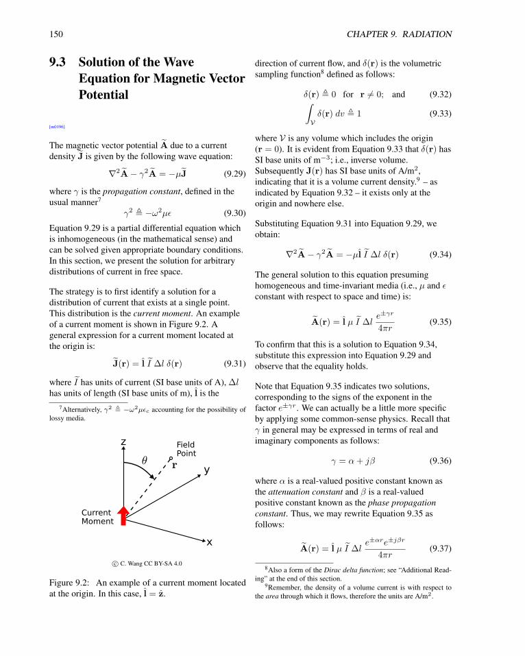
150 CHAPTER 9. RADIATION
9.3 Solution of the Wave
Equation for Magnetic Vector
Potential
[m0196]
The magnetic vector potential A due to a current
density J is given by the following wave equation:
∇2A− γ2A = −µJ (9.29)
where γ is the propagation constant, defined in the
usual manner7
γ2 , −ω2µǫ (9.30)
Equation 9.29 is a partial differential equation which
is inhomogeneous (in the mathematical sense) and
can be solved given appropriate boundary conditions.
In this section, we present the solution for arbitrary
distributions of current in free space.
The strategy is to first identify a solution for a
distribution of current that exists at a single point.
This distribution is the current moment. An example
of a current moment is shown in Figure 9.2. A
general expression for a current moment located at
the origin is:
J(r) = l I ∆l δ(r) (9.31)
where I has units of current (SI base units of A), ∆lhas units of length (SI base units of m), l is the
7Alternatively, γ2 , −ω2µǫc accounting for the possibility of
lossy media.
c© C. Wang CC BY-SA 4.0
Figure 9.2: An example of a current moment located
at the origin. In this case, l = z.
direction of current flow, and δ(r) is the volumetric
sampling function8 defined as follows:
δ(r) , 0 for r 6= 0; and (9.32)∫
V
δ(r) dv , 1 (9.33)
where V is any volume which includes the origin
(r = 0). It is evident from Equation 9.33 that δ(r) has
SI base units of m−3; i.e., inverse volume.
Subsequently J(r) has SI base units of A/m2,
indicating that it is a volume current density.9 – as
indicated by Equation 9.32 – it exists only at the
origin and nowhere else.
Substituting Equation 9.31 into Equation 9.29, we
obtain:
∇2A− γ2A = −µl I ∆l δ(r) (9.34)
The general solution to this equation presuming
homogeneous and time-invariant media (i.e., µ and ǫconstant with respect to space and time) is:
A(r) = l µ I ∆le±γr
4πr(9.35)
To confirm that this is a solution to Equation 9.34,
substitute this expression into Equation 9.29 and
observe that the equality holds.
Note that Equation 9.35 indicates two solutions,
corresponding to the signs of the exponent in the
factor e±γr. We can actually be a little more specific
by applying some common-sense physics. Recall that
γ in general may be expressed in terms of real and
imaginary components as follows:
γ = α+ jβ (9.36)
where α is a real-valued positive constant known as
the attenuation constant and β is a real-valued
positive constant known as the phase propagation
constant. Thus, we may rewrite Equation 9.35 as
follows:
A(r) = l µ I ∆le±αre±jβr
4πr(9.37)
8Also a form of the Dirac delta function; see “Additional Read-
ing” at the end of this section.9Remember, the density of a volume current is with respect to
the area through which it flows, therefore the units are A/m2.

9.3. SOLUTION OF THE WAVE EQUATION FOR MAGNETIC VECTOR POTENTIAL 151
Now consider the factor e±αr/r, which determines
the dependence of magnitude on distance r. If we
choose the negative sign in the exponent, this factor
decays exponentially with increasing distance from
the origin, ultimately reaching zero at r → ∞. This is
precisely the expected behavior, since we expect the
magnitude of a radiated field to diminish with
increasing distance from the source. If on the other
hand we choose the positive sign in the exponent, this
factor increases to infinity as r → ∞. That outcome
can be ruled out on physical grounds, since it implies
the introduction of energy independently from the
source. The requirement that field magnitude
diminishes to zero as distance from the source
increases to infinity is known as the radiation
condition, and is essentially a boundary condition that
applies at r → ∞. Invoking the radiation condition,
Equation 9.35 becomes:
A(r) = l µ I ∆le−γr
4πr(9.38)
In the loss-free (α = 0) case, we cannot rely on the
radiation condition to constrain the sign of γ.
However, in practical engineering work there is
always some media loss; i.e., α might be negligible
but is not quite zero. Thus, we normally assume that
the solution for lossless (including free space)
conditions is given by Equation 9.38 with α = 0:
A(r) = l µ I ∆le−jβr
4πr(9.39)
Now consider the factor e−jβr in Equation 9.39. This
factor exclusively determines the dependence of the
phase of A(r) with increasing distance r from the
source. In this case, we observe that surfaces of
constant phase correspond to spherical shells which
are concentric with the source. Thus, A(r) is a
spherical wave.
Let us now consider a slightly more complicated
version of the problem in which the current moment
is no longer located at the origin, but rather is located
at r′. This is illustrated in Figure 9.3. This current
distribution can be expressed as follows:
J(r) = l I ∆l δ(r− r′) (9.40)
The solution in this case amounts to a straightforward
modification of the existing solution. To see this, note
c© C. Wang CC BY-SA 4.0
Figure 9.3: Current moment displaced from the ori-
gin.
that A depends only on r, and not at all on θ or φ. In
other words, A depends only on the distance between
the “field point” r at which we observe A, and the
“source point” r′ at which the current moment lies.
Thus we replace r with this distance, which is
|r− r′|. The solution becomes:
A(r) = l µ I ∆le−γ|r−r
′|4π |r− r′| (9.41)
Continuing to generalize the solution, let us now
consider a scenario consisting of a filament of current
following a path C through space. This is illustrated in
Figure 9.4. Such a filament may be viewed as a
collection of a large number N of discrete current
moments distributed along the path. The contribution
of the nth current moment, located at rn, to the total
magnetic vector potential is:
∆A(r; rn) = l(rn) µ I(rn) ∆le−γ|r−rn|
4π |r− rn|(9.42)
Note that we are allowing both the current I and
current direction l to vary with position along C.
Assuming the medium is linear, superposition applies.
So we add these contributions to obtain the total

152 CHAPTER 9. RADIATION
c© C. Wang CC BY-SA 4.0
Figure 9.4: A filament of current lying along the path
C. This current distribution may be interpreted as a
collection of current moments lying along C.
magnetic vector potential:
A(r) ≈N∑
n=1
∆A(r; rn) (9.43)
≈ µ
4π
N∑
n=1
l(rn) I(rn)e−γ|r−rn|
|r− rn|∆l (9.44)
Now letting ∆l → 0 so that we may replace ∆l with
the differential length dl:
A(r) =µ
4π
∫
C
l(r′) I(r′)e−γ|r−r
′||r− r′| dl (9.45)
where we have also replaced rn with the original
notation r′ since we once again have a continuum (as
opposed to a discrete set) of source locations.
The magnetic vector potential corresponding to
radiation from a line distribution of current is
given by Equation 9.45.
Given A(r), the magnetic and electric fields may be
determined using the procedure developed in
Section 9.2.
Additional Reading:
• “Magnetic potential” on Wikipedia.
• “Dirac delta function” on Wikipedia.
9.4 Radiation from a Hertzian
Dipole
[m0197]
Section 9.1 presented an informal derivation of the
electromagnetic field radiated by a Hertzian dipole
represented by a zero-length current moment. In this
section, we provide a rigorous derivation using the
concept of magnetic vector potential discussed in
Sections 9.2 and 9.3. A review of those sections is
recommended before tackling this section.
A Hertzian dipole is commonly defined as an
electrically-short and infinitesimally-thin straight
filament of current, in which the density of the current
is uniform over its length. The Hertzian dipole is
commonly used as a “building block” for constructing
physically-realizable distributions of current as
exhibited by devices such as wire antennas. The
method is to model these relatively complex
distributions of current as the sum of Hertzian dipoles,
which reduces the problem to that of summing the
contributions of the individual Hertzian dipoles, with
each Hertzian dipole having the appropriate (i.e.,
different) position, magnitude, and phase.
To facilitate use of the Hertzian dipole as a building
block suitable for constructing physically-realizable
distributions of current, we choose to represent the
Hertzian dipole using an essentially equivalent current
distribution which is mathematically more versatile.
This description of the Hertzian dipole replaces the
notion of constant current over finite length with the
notion of a current moment located at a single point.
This is shown in Figure 9.5, and is given by:
∆J(r) = l I ∆l δ(r) (9.46)
where the product I∆l (SI base units of A·m) is the
current moment, l is the direction of current flow, and
δ(r) is the volumetric sampling function defined as
follows:
δ(r) , 0 for r 6= 0; and (9.47)∫
V
δ(r) dv , 1 (9.48)
where V is any volume which includes the origin
(r = 0). In this description, the Hertzian dipole is
located at the origin.

9.4. RADIATION FROM A HERTZIAN DIPOLE 153
The solution for the magnetic vector potential due to a
z-directed Hertzian dipole located at the origin was
presented in Section 9.3. In the present scenario, it is:
A(r) = z µ I ∆le−γr
4πr(9.49)
where the propagation constant γ = α+ jβ as usual.
Assuming lossless media (α = 0), we have
A(r) = z µ I ∆le−jβr
4πr(9.50)
We obtain the magnetic field intensity using the
definition of magnetic vector potential:
H , (1/µ)∇× A (9.51)
=I ∆l
4π∇× z
e−jβr
r(9.52)
To proceed, it is useful to convert z into the spherical
coordinate system. To do this, we find the component
of z that is parallel to r, θ, and φ; and then sum the
results:
z = r (r · z) + θ(θ · z
)+ φ
(φ · z
)(9.53)
= r cos θ − θ sin θ + 0 (9.54)
Equation 9.52 requires computation of the following
quantity:
∇× ze−jβr
r= ∇×
[r (cos θ)
e−jβr
r
−θ (sin θ) e−jβr
r
](9.55)
c© C. Wang CC BY-SA 4.0
Figure 9.5: A Hertzian dipole located at the origin,
represented as a current moment. In this case, l = z.
At this point, it is convenient to make the following
definitions:
Cr , (cos θ)e−jβr
r(9.56)
Cθ , − (sin θ)e−jβr
r(9.57)
These definitions allow Equation 9.55 to be written
compactly as follows:
∇× ze−jβr
r= ∇×
[rCr + θCθ
](9.58)
The right side of Equation 9.58 is evaluated using
Equation B.18 (Appendix B.2). Although the
complete expression consists of 6 terms, only 2 terms
are non-zero.10 This leaves:
∇× ze−jβr
r= φ
1
r
[∂
∂r(rCθ)−
∂
∂θCr
](9.59)
= φ (sin θ)e−jβr
r
(jβ +
1
r
)(9.60)
Substituting this result into Equation 9.52, we obtain:
H = φI ∆l
4π(sin θ)
e−jβr
r
(jβ +
1
r
)(9.61)
Let us further limit our scope to the field far from the
antenna. Specifically, let us assume r ≫ λ. Now we
use the relationship β = 2π/λ and determine the
following:
jβ +1
r= j
2π
λ+
1
r(9.62)
≈ j2π
λ= jβ (9.63)
Equation 9.61 becomes:
H ≈ φjI · β∆l4π
(sin θ)e−jβr
r(9.64)
where the approximation holds for low-loss media
and r ≫ λ. This expression is known as a far field
approximation, since it is valid only for distances
“far” (relative to a wavelength) from the source.
Now let us take a moment to interpret this result:
10Specifically, two terms are zero because there is no φ compo-
nent in the argument of the curl function; and another two terms are
zero because the argument of the curl function is independent of φ,
so partial derivatives with respect to φ are zero.

154 CHAPTER 9. RADIATION
• Notice the factor β∆l has units of radians; that
is, it is electrical length. This tells us that the
magnitude of the radiated field depends on the
electrical length of the current moment.
• The factor e−jβr/r indicates that this is a
spherical wave; that is, surfaces of constant
phase correspond to concentric spheres centered
on the source, and magnitude is inversely
proportional to distance.
• The direction of the magnetic field vector is
always φ, which is precisely what we expect; for
example, using the Biot-Savart law.
• Finally, note the factor sin θ. This indicates that
the field magnitude is zero along the direction in
which the source current flows, and is a
maximum in the plane perpendicular to this
direction.
Now let us determine the electric field radiated by the
Hertzian dipole. The direct method is to employ
Ampere’s law. That is,
E =1
jωǫ∇× H (9.65)
where H is given by Equation 9.64. At field points far
from the dipole, the radius of curvature of the
spherical phasefronts is very large and so appear to be
locally planar. That is, from the perspective of an
observer far from the dipole, the arriving wave
appears to be a plane wave. In this case, we may
employ the plane wave relationships. The appropriate
relationship in this case is:
E = −ηr× H (9.66)
where η is the wave impedance. So we find:
E ≈ θjηI · β∆l4π
(sin θ)e−jβr
r(9.67)
Summarizing:
The electric and magnetic fields far (i.e., ≫ λ)
from a z-directed Hertzian dipole having con-
stant current I over length ∆l, located at the ori-
gin, are given by Equations 9.67 and 9.64, respec-
tively.
Additional Reading:
• “Dipole antenna” (section entitled “Hertzian
Dipole”) on Wikipedia.

9.5. RADIATION FROM AN ELECTRICALLY-SHORT DIPOLE 155
9.5 Radiation from an
Electrically-Short Dipole
[m0198]
The simplest distribution of radiating current that is
encountered in common practice is the
electrically-short dipole (ESD). This current
distribution is shown in Figure 9.6. The two
characteristics that define the ESD are (1) the current
is aligned along a straight line, and (2) the length L of
the line is much less than one-half of a wavelength;
i.e., L≪ λ/2. The latter characteristic is what we
mean by “electrically-short.”11
The current distribution of an ESD is approximately
triangular in magnitude, and approximately constant
in phase. How do we know this? First, note that
distributions of current cannot change in a complex or
rapid way over such distances which are much less
than a wavelength. If this is not immediately
apparent, recall the behavior of transmission lines:
11A potential source of confusion is that the Hertzian dipole is
also a “dipole” which is “electrically-short.” The distinction is that
the current comprising a Hertzian dipole is constant over its length.
This condition is rarely and only approximately seen in practice,
whereas the triangular magnitude distribution is a relatively good ap-
proximation to a broad class of commonly-encountered electrically-
short wire antennas. Thus, the term “electrically-short dipole,” as
used in this book, refers to the triangular distribution unless noted
otherwise.
c© C. Wang CC BY-SA 4.0
Figure 9.6: Current distribution of the electrically-
short dipole (ESD).
c© C. Wang CC BY-SA 4.0
Figure 9.7: Current distribution of the electrically-
short dipole (ESD) approximated as a large number of
Hertzian dipoles.
The current standing wave on a transmission line
exhibits a period of λ/2, regardless the source or
termination. For the ESD, L≪ λ/2 and so we expect
an even simpler variation. Also, we know that the
current at the ends of the dipole must be zero, simply
because the dipole ends there. These considerations
imply that the current distribution of the ESD is
well-approximated as triangular in magnitude.12
Expressed mathematically:
I(z) ≈ I0
(1− 2
L|z|)
(9.68)
where I0 (SI base units of A) is a complex-valued
constant indicating the maximum current magnitude
and phase.
There are two approaches that we might consider in
order to find the electric field radiated by an ESD. The
first approach is to calculate the magnetic vector
potential A by integration over the current
distribution, calculate H = (1/µ)∇× A, and finally
calculate E from H using Ampere’s law. We shall
employ a simpler approach, shown in Figure 9.7.
Imagine the ESD as a collection of many shorter
segments of current that radiate independently. The
total field is then the sum of these short segments.
Because these segments are very short relative to the
12A more rigorous analysis leading to the same conclusion is pos-
sible, but is beyond the scope of this book.

156 CHAPTER 9. RADIATION
length of the dipole as well as being short relative to a
wavelength, we may approximate the current over
each segment as approximately constant. In other
words, we may interpret each of these segments as
being, to a good approximation, a Hertzian dipole.
The advantage of this approach is that we already
have a solution for each of the segments. In
Section 9.4, it is shown that a z-directed Hertzian
dipole at the origin radiates the electric field
E(r) ≈ θjηI · β∆l4π
(sin θ)e−jβr
r(9.69)
where I and ∆l may be interpreted as the current and
length of the dipole, respectively. In this expression, ηis the wave impedance of medium in which the dipole
radiates (e.g., ≈ 377 Ω for free space), and we have
presumed lossless media such that the attenuation
constant α ≈ 0 and the phase propagation constant
β = 2π/λ. This expression also assumes field points
far from the dipole; specifically, distances r that are
much greater than λ. Repurposing this expression for
the present problem, the segment at the origin radiates
the electric field:
E(r; z′ = 0) ≈ θjηI0 · β∆l
4π(sin θ)
e−jβr
r(9.70)
where the notation z′ = 0 indicates the Hertzian
dipole is located at the origin. Letting the length ∆lof this segment shrink to differential length dz′, we
may describe the contribution of this segment to the
field radiated by the ESD as follows:
dE(r; z′ = 0) ≈ θjηI0 · βdz′
4π(sin θ)
e−jβr
r(9.71)
Using this approach, the electric field radiated by any
segment can be written:
dE(r; z′) ≈ θ′jηβI(z′)
4π(sin θ′)
e−jβ|r−zz′||r− zz′| dz′
(9.72)
Note that θ is replaced by θ′ since the ray r− zz′
forms a different angle (i.e., θ′) with respect to z.
Similarly, θ is replaced by θ′, since it also varies with
z′. The electric field radiated by the ESD is obtained
by integration over these contributions:
E(r) ≈∫ +L/2
−L/2
dE(r; z′) (9.73)
c© C. Wang CC BY-SA 4.0
Figure 9.8: Parallel ray approximation for an ESD.
yielding:
E(r) ≈ jηβ
4π
∫ +L/2
−L/2
θ′I(z′) (sin θ′)e−jβ|r−zz′||r− zz′| dz′
(9.74)
Given some of the assumptions we have already
made, this expression can be further simplified. For
example, note that θ′ ≈ θ since L≪ r. For the same
reason, θ′ ≈ θ. Since these variables are
approximately constant over the length of the dipole,
we may move them outside the integral, yielding:
E(r) ≈ θjηβ
4π(sin θ)
∫ +L/2
−L/2
I(z′)e−jβ|r−zz′||r− zz′| dz′
(9.75)
It is also possible to simplify the expression |r− zz′|.Consider Figure 9.8. Since we have already assumed
that r ≫ L (i.e., the distance to field points is much
greater than the length of the dipole), the vector r is
approximately parallel to the vector r− zz′.Subsequently, it must be true that
|r− zz′| ≈ r − r · zz′ (9.76)
Note that the magnitude of r − r · zz′ must be
approximately equal to r, since r ≫ L. So, insofar as
|r− zz′| determines the magnitude of E(r), we may
use the approximation:
|r− zz′| ≈ r (magnitude) (9.77)
Insofar as |r− zz′| determines phase, we have to be a
bit more careful. The part of the integrand of
9.5. RADIATION FROM AN ELECTRICALLY-SHORT DIPOLE 157
Equation 9.75 that exhibits varying phase is
e−jβ|r−zz′|. Using Equation 9.76, we find
e−jβ|r−zz′| ≈ e−jβre+jβr·zz′
(9.78)
The worst case in terms of phase variation within the
integral is for field points along the z axis. For these
points, r · z = ±1 and subsequently |r− zz′| varies
from z − L/2 to z + L/2 where z is the location of
the field point. However, since L≪ λ (i.e., because
the dipole is electrically short), this difference in
lengths is much less than λ/2. Therefore, the phase
βr · zz′ varies by much less than π radians, and
subsequently e−jβr·zz′ ≈ 1. We conclude that under
these conditions,
e−jβ|r−zz′| ≈ e−jβr (phase) (9.79)
Applying these simplifications for magnitude and
phase to Equation 9.75, we obtain:
E(r) ≈ θjηβ
4π(sin θ)
e−jβr
r
∫ +L/2
−L/2
I(z′)dz′
(9.80)
The integral in this equation is very easy to evaluate;
in fact, from inspection (Figure 9.6), we determine it
is equal to I0L/2. Finally, we obtain:
E(r) ≈ θjηI0 · βL8π
(sin θ)e−jβr
r(9.81)
Summarizing:
The electric field intensity radiated by an ESD lo-
cated at the origin and aligned along the z axis is
given by Equation 9.81. This expression is valid
for r ≫ λ.
It is worth noting that the variation in magnitude,
phase, and polarization of the ESD with field point
location is identical to that of a single Hertzian dipole
having current moment zI0L/2 (Section 9.4).
However, the magnitude of the field radiated by the
ESD is exactly one-half that of the Hertzian dipole.
Why one-half? Simply because the integral over the
triangular current distribution assumed for the ESD is
one-half the integral over the uniform current
distribution that defines the Hertzian dipole. This
similarly sometimes causes confusion between
Hertzian dipoles and ESDs. Remember that ESDs are
physically realizable, whereas Hertzian dipoles are
not.
It is common to eliminate the factor of β in the
magnitude using the relationship β = 2π/λ, yielding:
E(r) ≈ θjηI04
L
λ(sin θ)
e−jβr
r(9.82)
At field points r ≫ λ, the wave appears to be locally
planar. Therefore, we are justified using the plane
wave relationship H = 1η r× E to calculate H. The
result is:
H(r) ≈ φjI04
L
λ(sin θ)
e−jβr
r(9.83)
Finally, let us consider the spatial characteristics of
the radiated field. Figures 9.9 and 9.10 show the
result in a plane of constant φ. Figures 9.11 and 9.12
show the result in the z = 0 plane. Note that the
orientations of the electric and magnetic field vectors
indicate a Poynting vector E× H that is always
directed radially outward from the location of the
dipole. This confirms that power flow is always
directed radially outward from the dipole. Due to the
symmetry of the problem, Figures 9.9–9.12 provide a
complete characterization of the relative magnitudes
and orientations of the radiated fields.

158 CHAPTER 9. RADIATION
c© S. Lally CC BY-SA 4.0
Figure 9.9: Magnitude of the radiated field in any
plane of constant φ.
c© S. Lally CC BY-SA 4.0
Figure 9.10: Orientation of the electric and magnetic
fields in any plane of constant φ.
c© S. Lally CC BY-SA 4.0
Figure 9.11: Magnitude of the radiated field in any
plane of constant z.
c© S. Lally CC BY-SA 4.0
Figure 9.12: Orientation of the electric and magnetic
fields in the z = 0 plane.

9.6. FAR-FIELD RADIATION FROM A THIN STRAIGHT FILAMENT OF CURRENT 159
9.6 Far-Field Radiation from a
Thin Straight Filament of
Current
[m0199]
A simple distribution of radiating current that is
encountered in common practice is the thin straight
current filament, shown in Figure 9.13. The defining
characteristic of this distribution is that the current
filament is aligned along a straight line, and that the
maximum dimension of the cross-section of the
filament is much less than a wavelength. The latter
characteristic is what we mean by “thin” – i.e., the
filament is “electrically thin.” Physical distributions
of current that meet this description include the
electrically-short dipole (Section 9.5) and the
half-wave dipole (Section 9.7) among others. A
gentler introduction to this distribution is via
Section 9.5 (“Radiation from an Electrically-Short
Dipole”), so students may want to review that section
first. This section presents the more general case.
Let the magnitude and phase of current along the
filament be given by the phasor quantity I(z) (SI base
units of A). In principle, the only constraint on I(z)
c© C. Wang CC BY-SA 4.0
Figure 9.13: A thin straight distribution of radiating
current.
c© C. Wang CC BY-SA 4.0
Figure 9.14: Current distribution approximated as a
set of Hertzian dipoles.
that applies generally is that it must be zero at the
ends of the distribution; i.e., I(z) = 0 for |z| ≥ L/2.
Details beyond this constraint depend on L and
perhaps other factors. Nevertheless, the
characteristics of radiation from members of this class
of current distributions have much in common,
regardless of L. These become especially apparent if
we limit our scope to field points far from the current,
as we shall do here.
There are two approaches that we might consider in
order to find the electric field radiated by this
distribution. The first approach is to calculate the
magnetic vector potential A by integration over the
current distribution (Section 9.3), calculate
H = (1/µ)∇× A, and finally calculate E from H
using the differential form of Ampere’s law. In this
section, we shall employ a simpler approach, shown
in Figure 9.14. Imagine the filament as a collection of
many shorter segments of current that radiate
independently. The total field is then the sum of these
short segments. Because these segments are very
short relative to the length of the filament as well as
being short relative to a wavelength, we may
approximate the current over each segment as
constant. In other words, we may interpret each
segment as being, to a good approximation, a
Hertzian dipole.
The advantage of this approach is that we already
have a solution for every segment. In Section 9.4, it is

160 CHAPTER 9. RADIATION
shown that a z-directed Hertzian dipole at the origin
radiates the electric field
E(r) ≈ θjηI (β∆l)
4π(sin θ)
e−jβr
r(9.84)
where I and ∆l may be interpreted as the current and
length of the filament, respectively. In this expression,
η is the wave impedance of medium in which the
filament radiates (e.g., ≈ 377 Ω for free space), and
we have presumed lossless media such that the
attenuation constant α ≈ 0 and the phase propagation
constant β = 2π/λ. This expression also assumes
field points far from the filament; specifically,
distances r that are much greater than λ. Repurposing
this expression for the present problem, we note that
the segment at the origin radiates the electric field:
E(r; z′ = 0) ≈ θjηI(0) (β∆l)
4π(sin θ)
e−jβr
r(9.85)
where the notation z′ = 0 indicates the Hertzian
dipole is located at the origin. Letting the length ∆lof this segment shrink to differential length dz′, we
may describe the contribution of this segment to the
field radiated by the ESD as follows:
dE(r; z′ = 0) ≈ θjηI(0) (βdz′)
4π(sin θ)
e−jβr
r(9.86)
Using this approach, the electric field radiated by any
segment can be written:
dE(r; z′) ≈ θ′jηβI(z′)
4π(sin θ′)
e−jβ|r−zz′||r− zz′| dz′
(9.87)
Note that θ is replaced by θ′ since the ray r− zz′
forms a different angle (i.e., θ′) with respect to z.
Subsequently, θ is replaced by θ′, which varies
similarly with z′. The electric field radiated by the
filament is obtained by integration over these
contributions, yielding:
E(r) ≈∫ +L/2
−L/2
dE(r; z′) (9.88)
Expanding this expression:
E(r) ≈ jηβ
4π
∫ +L/2
−L/2
θ′I(z′) (sin θ′)e−jβ|r−zz′||r− zz′| dz′
(9.89)
c© C. Wang CC BY-SA 4.0
Figure 9.15: Parallel ray approximation.
Given some of the assumptions we have already
made, this expression can be further simplified. For
example, note that θ′ ≈ θ since L≪ r. For the same
reason, θ′ ≈ θ. Since these variables are
approximately constant over the length of the
filament, we may move them outside the integral,
yielding:
E(r) ≈ θjηβ
4π(sin θ)
∫ +L/2
−L/2
I(z′)e−jβ|r−zz′||r− zz′| dz′
(9.90)
It is also possible to simplify the expression |r− zz′|.Consider Figure 9.15. Since we have already assumed
that r ≫ L (i.e., the distance to field points is much
greater than the length of the filament), the vector r is
approximately parallel to the vector r− zz′.Subsequently, it must be true that
|r− zz′| ≈ r − r · zz′ (9.91)
≈ r − z′ cos θ (9.92)
Note that the magnitude of r − r · zz′ must be
approximately equal to r, since r ≫ L. So, insofar as
|r− zz′| determines the magnitude of E(r), we may
use the approximation:
|r− zz′| ≈ r (magnitude) (9.93)
Insofar as |r− zz′| determines phase, we have to be
more careful. The part of the integrand of
Equation 9.90 that exhibits varying phase is
e−jβ|r−zz′|. Using Equation 9.91, we find
e−jβ|r−zz′| ≈ e−jβre+jβz′ cos θ (9.94)

9.7. FAR-FIELD RADIATION FROM A HALF-WAVE DIPOLE 161
These simplifications are known collectively as a far
field approximation, since they are valid only for
distances “far” from the source.
Applying these simplifications for magnitude and
phase to Equation 9.90, we obtain:
E(r) ≈ θjηβ
4π
e−jβr
r(sin θ)
·∫ +L/2
−L/2
I(z′)e+jβz′ cos θdz′ (9.95)
Finally, it is common to eliminate the factor of β in
the magnitude using the relationship β = 2π/λ,
yielding:
E(r) ≈ θjη
2
e−jβr
r(sin θ)
·[1
λ
∫ +L/2
−L/2
I(z′)e+jβz′ cos θdz′
](9.96)
The electric field radiated by a thin, straight, z-
directed current filament of length L located at
the origin and aligned along the z axis is given
by Equation 9.96. This expression is valid for
r ≫ L and r ≫ λ.
At field points satisfying the conditions r ≫ L and
r ≫ λ, the wave appears to be locally planar.
Therefore, we are justified using the plane wave
relationship H = (1/η)r× E to calculate H.
As a check, one may readily verify that Equation 9.96
yields the expected result for the electrically-short
dipole (Section 9.5).
9.7 Far-Field Radiation from a
Half-Wave Dipole
[m0200]
A simple and important current distribution is that of
the thin half-wave dipole (HWD), shown in
Figure 9.16. This is the distribution expected on a thin
straight wire having length L = λ/2, where λ is
wavelength. This distribution is described
mathematically as follows:
I(z) ≈ I0 cos(πz
L
)for |z| ≤ L
2(9.97)
where I0 (SI base units of A) is a complex-valued
constant indicating the maximum magnitude of the
current and its phase. Note that the current is zero at
the ends of the dipole; i.e., I(z) = 0 for |z| = L/2.
Note also that this “cosine pulse” distribution is very
similar to the triangular distribution of the ESD, and
is reminiscent of the sinusoidal variation of current in
a standing wave.
Since L = λ/2 for the HWD, Equation 9.97 may
equivalently be written:
I(z) ≈ I0 cos(2πz
λ
)(9.98)
The electromagnetic field radiated by this distribution
c© C. Wang CC BY-SA 4.0
Figure 9.16: Current distribution of the half-wave
dipole (HWD).

162 CHAPTER 9. RADIATION
of current may be calculated using the method
described in Section 9.6, in particular:
E(r) ≈ θjη
2
e−jβr
r(sin θ)
·[1
λ
∫ +L/2
−L/2
I(z′)e+jβz′ cos θdz′
](9.99)
which is valid for field points r far from the dipole;
i.e., for r ≫ L and r ≫ λ. For the HWD, the quantity
in square brackets is
I0λ
∫ +λ/4
−λ/4
cos
(2πz′
λ
)e+jβz
′ cos θdz′ (9.100)
The evaluation of this integral is straightforward, but
tedious. The integral reduces to
I0π
cos [(π/2) cos θ]
sin2 θ(9.101)
Substitution into Equation 9.99 yields
E(r) ≈ θjηI02π
cos [(π/2) cos θ]
sin θ
e−jβr
r(9.102)
The magnetic field may be determined from this
result using Ampere’s law. However, a simpler
method is to use the fact that the electric field,
magnetic field, and direction of propagation r are
mutually perpendicular and related by:
H =1
ηr× E (9.103)
This relationship indicates that the magnetic field will
be +φ-directed.
The magnitude and polarization of the radiated field is
similar to that of the electrically-short dipole (ESD;
Section 9.5). A comparison of the magnitudes in any
radial plane containing the z-axis is shown in
Figure 9.17. For either current distribution, the
maximum magnitude of the fields occurs in the z = 0plane. For a given terminal current I0, the maximum
magnitude is greater for the HWD than for the ESD.
Both current distributions yield zero magnitude along
the axis of the dipole. The polarization characteristics
of the fields of both current distributions are identical.
Additional Reading:
• “Dipole antenna” (section entitled “Half-wave
dipole”) on Wikipedia.
c© C. Wang CC BY-SA 4.0
Figure 9.17: Comparison of the magnitude of the ra-
diated field of the HWD to that of an electrically-short
dipole also oriented along the z-axis. This result is for
any radial plane that includes the z-axis.
9.8 Radiation from Surface and
Volume Distributions of
Current
[m0221]
In Section 9.3, a solution was developed for radiation
from current located at a single point r′. This current
distribution was expressed mathematically as a
current moment, as follows:
J(r) = l I ∆l δ(r− r′) (9.104)
where l is the direction of current flow, I has units of
current (SI base units of A), ∆l has units of length (SI
base units of m), and δ(r) is the volumetric sampling
function (Dirac “delta” function; SI base units of
m−3). In this formulation, J has SI base units of
A/m2. The magnetic vector potential radiated by this
current, observed at the field point r, was found to be
A(r) = l µ I ∆le−γ|r−r
′|4π |r− r′| (9.105)
This solution was subsequently generalized to obtain
the radiation from any distribution of line current; i.e.,

9.8. RADIATION FROM SURFACE AND VOLUME DISTRIBUTIONS OF CURRENT 163
any distribution of current that is constrained to flow
along a single path through space, as along an
infinitesimally-thin wire.
In this section, we derive an expression for the
radiation from current that is constrained to flow
along a surface and from current which flows through
a volume. The solution in both cases can be obtained
by “recycling” the solution for line current as follows.
Letting ∆l shrink to the differential length dl,Equation 9.104 becomes:
dJ(r) = l I dl δ(r− r′) (9.106)
Subsequently, Equation 9.105 becomes:
dA(r; r′) = l µ I dle−γ|r−r
′|4π |r− r′| (9.107)
where the notation dA(r; r′) is used to denote the
magnetic vector potential at the field point r due to
the differential-length current moment at the source
point r′. Next, consider that any distribution of
current can be described as a distribution of current
moments. By the principle of superposition, the
radiation from this distribution of current moments
can be calculated as the sum of the radiation from the
individual current moments. This is expressed
mathematically as follows:
A(r) =
∫dA(r; r′) (9.108)
where the integral is over r′; i.e., summing over the
source current.
If we substitute Equation 9.107 into Equation 9.108,
we obtain the solution derived in Section 9.3, which is
specific to line distributions of current. To obtain the
solution for surface and volume distributions of
current, we reinterpret the definition of the differential
current moment in Equation 9.106. Note that this
current is completely specified by its direction (l) and
the quantity I dl, which has SI base units of A·m. We
may describe the same current distribution
alternatively as follows:
dJ(r) = l Js ds δ(r− r′) (9.109)
where Js has units of surface current density (SI base
units of A/m) and ds has units of area (SI base units
of m2). To emphasize that this is precisely the same
current moment, note that Js ds, like I dl, has units
of A·m. Similarly,
dJ(r) = l J dv δ(r− r′) (9.110)
where J has units of volume current density (SI base
units of A/m2) and dv has units of volume (SI base
units of m3). Again, J dv has units of A·m.
Summarizing, we have found that
I dl = Js ds = J dv (9.111)
all describe the same differential current moment.
Thus, we may obtain solutions for surface and volume
distributions of current simply by replacing I dl in
Equation 9.107, and subsequently in Equation 9.108,
with the appropriate quantity from Equation 9.111.
For a surface current distribution, we obtain:
A(r) =µ
4π
∫
S
Js(r′)e−γ|r−r
′||r− r′| ds (9.112)
where Js(r′) , l(r′)Js(r
′) and where S is the
surface over which the current flows. Similarly for a
volume current distribution, we obtain:
A(r) =µ
4π
∫
V
J(r′)e−γ|r−r
′||r− r′| dv (9.113)
where J(r′) , l(r′)J(r′) and where V is the volume
in which the current flows.
The magnetic vector potential corresponding to
radiation from a surface and volume distribution
of current is given by Equations 9.112 and 9.113,
respectively.
Given A(r), the magnetic and electric fields may be
determined using the procedure developed in
Section 9.2.
[m0217]

164 CHAPTER 9. RADIATION
Image Credits
Fig. 9.1: c© Sevenchw (C. Wang),
https://commons.wikimedia.org/wiki/File:A z-directed current moment located at the origin.svg,
CC BY-SA 4.0 (https://creativecommons.org/licenses/by-sa/4.0/).
Fig. 9.2: c© Sevenchw (C. Wang),
https://commons.wikimedia.org/wiki/File:A z-directed current moment located at the origin.svg,
CC BY-SA 4.0 (https://creativecommons.org/licenses/by-sa/4.0/).
Fig. 9.3: c© Sevenchw (C. Wang),
https://commons.wikimedia.org/wiki/File:Current moment displaced from the origin.svg,
CC BY-SA 4.0 (https://creativecommons.org/licenses/by-sa/4.0/).
Fig. 9.4: c© Sevenchw (C. Wang),
https://commons.wikimedia.org/wiki/File:A filament of current lying along the path c.svg,
CC BY-SA 4.0 (https://creativecommons.org/licenses/by-sa/4.0/).
Fig. 9.5: c© Sevenchw (C. Wang),
https://commons.wikimedia.org/wiki/File:A z-directed current moment located at the origin.svg,
CC BY-SA 4.0 (https://creativecommons.org/licenses/by-sa/4.0/).
Fig. 9.6: c© Sevenchw (C. Wang),
https://commons.wikimedia.org/wiki/File:Current distribution of the esd.svg,
CC BY-SA 4.0 (https://creativecommons.org/licenses/by-sa/4.0/).
Fig. 9.7: c© Sevenchw (C. Wang),
https://commons.wikimedia.org/wiki/File:Esd approximated as a large number of hertzian dipoles.svg,
CC BY-SA 4.0 (https://creativecommons.org/licenses/by-sa/4.0/).
Fig. 9.8: c© Sevenchw (C. Wang),
https://commons.wikimedia.org/wiki/File:Parallel ray approximation for an esd.svg,
CC BY-SA 4.0 (https://creativecommons.org/licenses/by-sa/4.0/).
Fig. 9.9: c© Offaperry (S. Lally),
https://commons.wikimedia.org/wiki/File:Magnitude of the Radiated Field.svg,
CC BY-SA 4.0 (https://creativecommons.org/licenses/by-sa/4.0/).
Fig. 9.10: c© Offaperry (S. Lally),
https://commons.wikimedia.org/wiki/File:Electric and Magnetic Fields in Plane of Constant Theta.svg,
CC BY-SA 4.0 (https://creativecommons.org/licenses/by-sa/4.0/).
Fig. 9.11: c© Offaperry (S. Lally), https://commons.wikimedia.org/wiki/File:FHplaneMag.svg,
CC BY-SA 4.0 (https://creativecommons.org/licenses/by-sa/4.0/).
Fig. 9.12: c© Offaperry (S. Lally), https://commons.wikimedia.org/wiki/File:FHplanePol.svg,
CC BY-SA 4.0 (https://creativecommons.org/licenses/by-sa/4.0/).
Fig. 9.13: c© Sevenchw (C. Wang),
https://commons.wikimedia.org/wiki/File:A thin straight distribution of radiating current.svg,
CC BY-SA 4.0 (https://creativecommons.org/licenses/by-sa/4.0/).
Fig. 9.14: c© Sevenchw (C. Wang),
https://commons.wikimedia.org/wiki/File:Esd approximated as a large number of hertzian dipoles.svg,
CC BY-SA 4.0 (https://creativecommons.org/licenses/by-sa/4.0/).

9.8. RADIATION FROM SURFACE AND VOLUME DISTRIBUTIONS OF CURRENT 165
Fig. 9.15: c© Sevenchw (C. Wang),
https://commons.wikimedia.org/wiki/File:Parallel ray approximation for an esd.svg,
CC BY-SA 4.0 (https://creativecommons.org/licenses/by-sa/4.0/).
Fig. 9.16: c© Sevenchw (C. Wang),
https://commons.wikimedia.org/wiki/File:Current distribution of the hwd.svg,
CC BY-SA 4.0 (https://creativecommons.org/licenses/by-sa/4.0/).
Fig. 9.17: c© Sevenchw (C. Wang),
https://commons.wikimedia.org/wiki/File:Comparison radiated field magnitude of hwd to esd.svg,
CC BY-SA 4.0 (https://creativecommons.org/licenses/by-sa/4.0/).

Chapter 10
Antennas
10.1 How Antennas Radiate
[m0201]
An antenna is a transducer; that is, a device which
converts signals in one form into another form. In the
case of an antenna, these two forms are (1)
conductor-bound voltage and current signals and (2)
electromagnetic waves. Traditional passive antennas
are capable of this conversion in either direction. In
this section, we consider the transmit case, in which a
conductor-bound signal is converted into a radiating
electromagnetic wave. Radiation from an antenna is
due to the time-varying current that is excited by the
bound electrical signal applied to the antenna
terminals.
Why ideal transmission lines don’t radiate. To
describe the process that allows an antenna to
transmit, it is useful to first consider the scenario
depicted in Figure 10.1. Here a sinusoidal source is
c© S. Lally CC BY-SA 4.0
Figure 10.1: Twin lead transmission line terminated
into an open circuit, giving rise to a standing wave.
applied to the input of an ideal twin lead transmission
line. The spacing between conductors is much less
than a wavelength, and the output of the transmission
line is terminated into an open circuit.
Without any additional information, we already know
two things about the current on this transmission line.
First, we know the current must be identically zero at
the end of the transmission line. Second, we know the
current on the two conductors comprising the
transmission line must be related as indicated in
Figure 10.1. That is, at any given position on the
transmission line, the current on each conductor is
equal in magnitude and flows in opposite directions.
Further note that Figure 10.1 depicts only the
situation over an interval of one-half of the period of
the sinusoidal source. For the other half-period, the
direction of current will be in the direction opposite
that depicted in Figure 10.1. In other words: The
source is varying periodically, so the sign of the
current is changing every half-period. Generally,
time-varying currents give rise to radiation.
Therefore, we should expect the currents depicted in
Figure 10.1 might radiate. We can estimate the
radiation from the transmission line by interpreting
the current as a collection of Hertzian dipoles. For a
review of Hertzian dipoles, see Section 9.4; however,
all we need to know to address the present problem is
that superposition applies. That is, the total radiation
is the sum of the radiation from the individual
Hertzian dipoles. Once again looking back at
Figure 10.1, note that each Hertzian dipole
representing current on one conductor has an
associated Hertzian dipole representing the current on
the other conductor, and is only a tiny fraction of a
wavelength distant. Furthermore, these pairs of
Electromagnetics Vol. 2. c© 2020 S.W. Ellingson CC BY SA 4.0. https://doi.org/10.21061/electromagnetics-vol-2

10.1. HOW ANTENNAS RADIATE 167
Hertzian dipoles are identical in magnitude but
opposite in sign. Therefore, the radiated field from
any such pair of Hertzian dipoles is approximately
zero at distances sufficiently far from the transmission
line. Continuing to sum all such pairs of Hertzian
dipoles, the radiated field remains approximately zero
at distances sufficiently far from the transmission line.
We come to the following remarkable conclusion:
The radiation from an ideal twin lead transmis-
sion line with open circuit termination is negligi-
ble at distances much greater than the separation
between the conductors.
Before proceeding, let us be clear about one thing:
The situation at distances which are not large relative
to separation between the conductors is quite
different. This is because the Hertzian dipole pairs do
not appear to be quite so precisely collocated at field
points close to the transmission line. Subsequently
the cancellation of fields from Hertzian dipole pairs is
less precise. The resulting sum fields are not
negligible and depend on the separation between the
conductors. For the present discussion, it suffices to
restrict our attention to the simpler “far field” case.
A simple antenna formed by modifying twin lead
transmission line. Let us now consider a
modification to the previous scenario, shown in
Figure 10.2. In the new scenario, the ends of the twin
lead are bent into right angles. This new section has
an overall length which is much less than one-half
wavelength. To determine the current distribution on
the modified section, we first note that the current
must still be precisely zero at the ends of the
conductors, but not necessarily at the point at which
c© S. Lally CC BY-SA 4.0
Figure 10.2: End of the twin lead transmission line
fashioned into an electrically-short dipole (ESD).
they are bent. Since the modified section is much
shorter than one-half wavelength, the current
distribution on this section must be very simple. In
fact, the current distribution must be that of the
electrically-short dipole (ESD), exhibiting magnitude
which is maximum at the center and decreasing
approximately linearly to zero at the ends. (See
Section 9.5 for a review of the ESD.) Finally, we note
that the current should be continuous at the junction
between the unmodified and modified sections.
Having established that the modified section exhibits
the current distribution of an ESD, and having
previously determined that the unmodified section of
transmission line does not radiate, we conclude that
this system radiates precisely as an ESD does. Note
also that we need not interpret the ESD portion of the
transmission line as a modification of the
transmission line: Instead, we may view this system
as an unmodified transmission line attached to an
antenna, which in this case in an ESD.
The general case. Although we developed this
insight for the ESD specifically, the principle applies
generally. That is, any antenna – not just dipoles –
can be viewed as a structure that can support a current
distribution that radiates. Elaborating:
A transmitting antenna is a device that, when
driven by an appropriate source, supports a time-
varying distribution of current resulting in an
electromagnetic wave that radiates away from the
device.
Although this may seem to be simply a restatement of
the definition at the beginning of this section – and it
is – we now see how this can happen, and also why
transmission lines typically aren’t also antennas.
168 CHAPTER 10. ANTENNAS
10.2 Power Radiated by an
Electrically-Short Dipole
[m0207]
In this section, we determine the total power radiated
by an electrically-short dipole (ESD) antenna in
response to a sinusoidally-varying current applied to
the antenna terminals. This result is both useful on its
own and necessary as an intermediate result in
determining the impedance of the ESD. The ESD is
introduced in Section 9.5, and a review of that section
is suggested before attempting this section.
In Section 9.5, it is shown that the electric field
intensity in the far field of a z-oriented ESD located at
the origin is
E(r) ≈ θjηI0 · βL8π
(sin θ)e−jβr
r(10.1)
where r is the field point, I0 is a complex number
representing the peak magnitude and phase of the
sinusoidally-varying terminal current, L is the length
of the ESD, and β is the phase propagation constant
2π/λ where λ is wavelength. Note that L≪ λ since
this is an ESD. Also note that Equation 10.1 is valid
only for the far-field conditions r ≫ L and r ≫ λ,
and presumes propagation in simple (linear,
homogeneous, time-invariant, isotropic) media with
negligible loss.
Given that we have already limited scope to the far
field, it is reasonable to approximate the
electromagnetic field at each field point r as a plane
wave propagating radially away from the antenna;
i.e., in the r direction. Under this assumption, the
time-average power density is
S(r) = r
∣∣∣E(r)∣∣∣2
2η(10.2)
where η is the wave impedance of the medium. The
total power Prad radiated by the antenna is simply
S(r) integrated over any closed surface S that
encloses the antenna. Thus:
Prad =
∮
S
S(r) · ds (10.3)
where ds is the outward-facing differential element of
surface area. In other words, power density (W/m2)
integrated over an area (m2) gives power (W).
Anticipating that this problem will be addressed in
spherical coordinates, we note that
ds = rr2 sin θ dθ dφ (10.4)
and subsequently:
Prad =
∫ π
θ=0
∫ 2π
φ=0
r
∣∣∣E(r)∣∣∣2
2η
·
(rr2 sin θ dθ dφ
)
=1
2η
∫ π
θ=0
∫ 2π
φ=0
∣∣∣E(r)∣∣∣2
r2 sin θ dθ dφ (10.5)
Returning to Equation 10.1, we note:
∣∣∣E(r)∣∣∣2
≈ η2|I0|2 (βL)2
64π2(sin θ)
2 1
r2(10.6)
Substitution into Equation 10.5 yields:
Prad ≈ η|I0|2 (βL)2
128π2
∫ π
θ=0
∫ 2π
φ=0
sin3 θ dθ dφ (10.7)
Note that this may be factored into separate integrals
over θ and φ. The integral over φ is simply 2π,
leaving:
Prad ≈ η|I0|2 (βL)2
64π
∫ π
θ=0
sin3 θ dθ (10.8)
The remaining integral is equal to 4/3, leaving:
Prad ≈ η|I0|2 (βL)2
48π(10.9)
This completes the derivation, but it is useful to check
units. Recall that β has SI base units of rad/m, so βLhas units of radians. This leaves η |I0|2, which has SI
base units of Ω · A2 = W, as expected.
The power radiated by an ESD in response to the
current I0 applied at the terminals is given by
Equation 10.9.
Finally, it is useful to consider how various
parameters affect the radiated power. First, note that
the radiated power is proportional to the square of the
terminal current. Second, note that the product
βL = 2πL/λ is the electrical length of the antenna;

10.3. POWER DISSIPATED BY AN ELECTRICALLY-SHORT DIPOLE 169
that is, the length of the antenna expressed in radians,
where 2π radians is one wavelength. Thus, we see
that the power radiated by the antenna increases as the
square of electrical length.
Example 10.1. Power radiated by an ESD.
A dipole is 10 cm in length and is surrounded by
free space. A sinusoidal current having
frequency 30 MHz and peak magnitude 100 mA
is applied to the antenna terminals. What is the
power radiated by the antenna?
Solution. If no power is dissipated within the
antenna, then all power is radiated. The
wavelength λ = c/f ∼= 10 m, so L ∼= 0.01λ.
This certainly qualifies as electrically-short, so
we may use Equation 10.9. In the present
problem, η ∼= 376.7 Ω (the free space wave
impedance), I0 = 100 mA, and
β = 2π/λ ∼= 0.628 rad/m. Thus, we find that the
radiated power is ≈ 98.6 µW.
10.3 Power Dissipated by an
Electrically-Short Dipole
[m0208]
The power delivered to an antenna by a source
connected to the terminals is nominally radiated.
However, it is possible that some fraction of the
power delivered by the source will be dissipated
within the antenna. In this section, we consider the
dissipation due to the finite conductivity of materials
comprising the antenna. Specifically, we determine
the total power dissipated by an electrically-short
dipole (ESD) antenna in response to a
sinusoidally-varying current applied to the antenna
terminals. (The ESD is introduced in Section 9.5, and
a review of that section is suggested before attempting
this section.) The result allows us to determine
radiation efficiency and is a step toward determining
the impedance of the ESD.
Consider an ESD centered at the origin and aligned
along the z axis. In Section 9.5, it is shown that the
current distribution is:
I(z) ≈ I0
(1− 2
L|z|)
(10.10)
where I0 (SI base units of A) is a complex-valued
constant indicating the maximum current magnitude
and phase, and L is the length of the ESD. This
current distribution may be interpreted as a set of
discrete very-short segments of constant-magnitude
current (sometimes referred to as “Hertzian dipoles”).
In this interpretation, the nth current segment is
located at z = zn and has magnitude I(zn).
Now let us assume that the material comprising the
ESD is a homogeneous good conductor. Then each
segment exhibits the same resistance Rseg .
Subsequently, the power dissipated in the nth
segment is
Pseg(zn) =1
2
∣∣∣I(zn)∣∣∣2
Rseg (10.11)
The segment resistance can be determined as follows.
Let us assume that the wire comprising the ESD has
circular cross-section of radius a. Since the wire is a
good conductor, the segment resistance may be
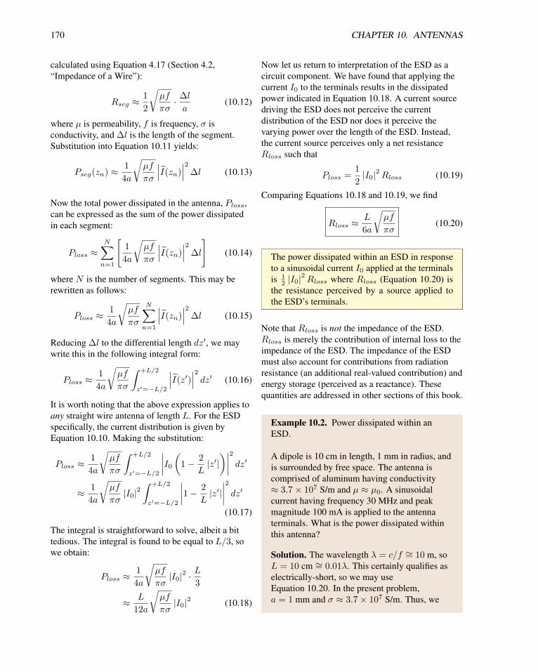
170 CHAPTER 10. ANTENNAS
calculated using Equation 4.17 (Section 4.2,
“Impedance of a Wire”):
Rseg ≈1
2
õf
πσ· ∆la
(10.12)
where µ is permeability, f is frequency, σ is
conductivity, and ∆l is the length of the segment.
Substitution into Equation 10.11 yields:
Pseg(zn) ≈1
4a
õf
πσ
∣∣∣I(zn)∣∣∣2
∆l (10.13)
Now the total power dissipated in the antenna, Ploss,can be expressed as the sum of the power dissipated
in each segment:
Ploss ≈N∑
n=1
[1
4a
õf
πσ
∣∣∣I(zn)∣∣∣2
∆l
](10.14)
where N is the number of segments. This may be
rewritten as follows:
Ploss ≈1
4a
õf
πσ
N∑
n=1
∣∣∣I(zn)∣∣∣2
∆l (10.15)
Reducing ∆l to the differential length dz′, we may
write this in the following integral form:
Ploss ≈1
4a
õf
πσ
∫ +L/2
z′=−L/2
∣∣∣I(z′)∣∣∣2
dz′ (10.16)
It is worth noting that the above expression applies to
any straight wire antenna of length L. For the ESD
specifically, the current distribution is given by
Equation 10.10. Making the substitution:
Ploss ≈1
4a
õf
πσ
∫ +L/2
z′=−L/2
∣∣∣∣I0(1− 2
L|z′|)∣∣∣∣
2
dz′
≈ 1
4a
õf
πσ|I0|2
∫ +L/2
z′=−L/2
∣∣∣∣1−2
L|z′|∣∣∣∣2
dz′
(10.17)
The integral is straightforward to solve, albeit a bit
tedious. The integral is found to be equal to L/3, so
we obtain:
Ploss ≈1
4a
õf
πσ|I0|2 ·
L
3
≈ L
12a
õf
πσ|I0|2 (10.18)
Now let us return to interpretation of the ESD as a
circuit component. We have found that applying the
current I0 to the terminals results in the dissipated
power indicated in Equation 10.18. A current source
driving the ESD does not perceive the current
distribution of the ESD nor does it perceive the
varying power over the length of the ESD. Instead,
the current source perceives only a net resistance
Rloss such that
Ploss =1
2|I0|2Rloss (10.19)
Comparing Equations 10.18 and 10.19, we find
Rloss ≈L
6a
õf
πσ(10.20)
The power dissipated within an ESD in response
to a sinusoidal current I0 applied at the terminals
is 12 |I0|
2Rloss where Rloss (Equation 10.20) is
the resistance perceived by a source applied to
the ESD’s terminals.
Note that Rloss is not the impedance of the ESD.
Rloss is merely the contribution of internal loss to the
impedance of the ESD. The impedance of the ESD
must also account for contributions from radiation
resistance (an additional real-valued contribution) and
energy storage (perceived as a reactance). These
quantities are addressed in other sections of this book.
Example 10.2. Power dissipated within an
ESD.
A dipole is 10 cm in length, 1 mm in radius, and
is surrounded by free space. The antenna is
comprised of aluminum having conductivity
≈ 3.7× 10⁷ S/m and µ ≈ µ0. A sinusoidal
current having frequency 30 MHz and peak
magnitude 100 mA is applied to the antenna
terminals. What is the power dissipated within
this antenna?
Solution. The wavelength λ = c/f ∼= 10 m, so
L = 10 cm ∼= 0.01λ. This certainly qualifies as
electrically-short, so we may use
Equation 10.20. In the present problem,
a = 1 mm and σ ≈ 3.7× 10⁷ S/m. Thus, we

10.4. REACTANCE OF THE ELECTRICALLY-SHORT DIPOLE 171
find that the loss resistance Rloss ≈ 9.49 mΩ.
Subsequently, the power dissipated within this
antenna is
Ploss =1
2|I0|2Rloss ≈ 47.5 µW (10.21)
We conclude this section with one additional caveat:
Whereas this section focuses on the limited
conductivity of wire, other physical mechanisms may
contribute to the loss resistance of the ESD. In
particular, materials used to coat the antenna or to
provide mechanical support near the terminals may
potentially absorb and dissipate power that might
otherwise be radiated.
10.4 Reactance of the
Electrically-Short Dipole
[m0210]
For any given time-varying voltage appearing across
the terminals of an electrically-short antenna, there
will be a time-varying current that flows in response.
The ratio of voltage to current is impedance. Just as a
resistor, capacitor, or inductor may be characterized
in terms of an impedance, any antenna may be
characterized in terms of this impedance. The
real-valued component of this impedance accounts for
power which is radiated away from the antenna
(Section 10.2) and dissipated within the antenna
(Section 10.3). The imaginary component of this
impedance – i.e., the reactance – typically represents
energy storage within the antenna, in the same way
that the reactance of a capacitor or inductor represents
storage of electrical or magnetic energy, respectively.
In this section, we determine the reactance of the
electrically-short dipole (ESD).
Reactance of a zero-length dipole. We begin with
what might seem initially to be an absurd notion: A
dipole antenna having zero length. However, such a
dipole is certainly electrically-short, and in fact serves
as an extreme condition from which we can deduce
some useful information.
Consider Figure 10.3, which shows a zero-length
dipole being driven by a source via a transmission
line. It is immediately apparent that such a dipole is
equivalent to an open circuit. So, the impedance of a
zero-length dipole is equal to that of an open circuit.
c© S. Lally CC BY-SA 4.0
Figure 10.3: Transmission line terminated into a zero-
length dipole, which is equivalent to an open circuit.
172 CHAPTER 10. ANTENNAS
What is the impedance of an open circuit? One might
be tempted to say “infinite,” since the current is zero
independently of the voltage. However, we must now
be careful to properly recognize the real and
imaginary components of this infinite number, and
signs of these components. In fact, the impedance of
an open circuit is 0− j∞. One way to confirm this is
via basic transmission line theory; i.e., the input
impedance of transmission line stubs. A more direct
justification is as follows: The real part of the
impedance is zero because there is no transfer of
power into the termination. The magnitude of the
imaginary part of the impedance must be infinite
because the current is zero. The sign of the imaginary
component is negative because the reflected current
experiences a sign change (required to make the total
current zero), whereas the reflected voltage does not
experience a sign change (and so is not canceled at
the terminals). Thus, the impedance of an open
circuit, and the zero-length dipole, is 0− j∞.
Reactance of a nearly-zero-length dipole. Let us
now consider what happens as the length of the dipole
increases from zero. Since such a dipole is short
compared to a wavelength, the variation with length
must be very simple. The reactance remains large and
negative, but can only increase (become less negative)
monotonically with increasing electrical length. This
trend continues until the dipole is no longer
electrically short. Thus, we conclude that the
reactance of an ESD is always large and negative.
The reactance of an ESD is very large and nega-
tive, approaching the reactance of an open circuit
termination as length decreases to zero.
Note that this behavior is similar to that of a capacitor,
whose impedance is also negative and increases
toward zero with increasing frequency. Thus, the
reactance of an ESD is sometimes represented in
circuit diagrams as a capacitor. However, the specific
dependence of reactance on frequency is different
from that of a capacitor (as we shall see in a moment),
so this model is generally valid only for analysis at
one frequency at time.
An approximate expression for the reactance of an
ESD. Sometimes it is useful to be able to estimate the
reactance XA of an ESD. Although a derivation is
beyond the scope of this text, a suitable expression is
(see, e.g., Johnson (1993) in “Additional References”
at the end of this section):
XA ≈ −120 Ω
πL/λ
[ln
(L
2a
)− 1
](10.22)
where L is length and a≪ L is the radius of the wire
comprising the ESD. Note that this expression yields
the expected behavior; i.e., XA → −∞ as L→ 0,
and increases monotonically as L increases from zero.
Example 10.3. Reactance of an ESD.
A dipole is 10 cm in length, 1 mm in radius, and
is surrounded by free space. What is the
reactance of this antenna at 30 MHz?
Solution. The wavelength λ = c/f ∼= 10 m, so
L = 10 cm ∼= 0.01λ. This certainly qualifies as
electrically-short, so we may use
Equation 10.22. Given a = 1 mm, we find the
reactance XA ≈ −11.1 kΩ. For what it’s worth,
this antenna exhibits approximately the same
reactance as a 0.47 pF capacitor at the same
frequency.
The reactance of the ESD is typically orders of
magnitude larger than the real part of the impedance
of the ESD. The reactance of the ESD is also typically
very large compared to the characteristic impedance
of typical transmission lines (usually 10s to 100s of
ohms). This makes ESDs quite difficult to use in
practical transmit applications.
Additional Reading:
• R.C. Johnson (Ed.), Antenna Systems Handbook
(Ch. 4), McGraw-Hill, 1993.

10.5. EQUIVALENT CIRCUIT MODEL FOR TRANSMISSION; RADIATION EFFICIENCY 173
10.5 Equivalent Circuit Model
for Transmission; Radiation
Efficiency
[m0202]
A radio transmitter consists of a source which
generates the electrical signal intended for
transmission, and an antenna which converts this
signal into a propagating electromagnetic wave. Since
the transmitter is an electrical system, it is useful to be
able to model the antenna as an equivalent circuit.
From a circuit analysis point of view, it should be
possible to describe the antenna as a passive one-port
circuit that presents an impedance to the source.
Thus, we have the following question: What is the
equivalent circuit for an antenna which is
transmitting?
We begin by emphasizing that the antenna is passive.
That is, the antenna does not add power. Invoking the
principle of conservation of power, there are only
three possible things that can happen to power that is
delivered to the antenna by the transmitter:1
• Power can be converted to a propagating
electromagnetic wave. (The desired outcome.)
• Power can be dissipated within the antenna.
• Energy can be stored by the antenna, analogous
to the storage of energy in a capacitor or
inductor.
We also note that these outcomes can occur in any
combination. Taking this into account, we model the
antenna using the equivalent circuit shown in
Figure 10.4. Since the antenna is passive, it is
reasonable to describe it as an impedance ZA which
is (by definition) the ratio of voltage VA to current IAat the terminals; i.e.,
ZA ,VA
IA(10.23)
1Note that “delivered” power means power accepted by the an-
tenna. We are not yet considering power reflected from the antenna
due to impedance mismatch.
In the phasor domain, ZA is a complex-valued
quantity and therefore has, in general, a real-valued
component and an imaginary component. We may
identify those components using the power
conservation argument made previously: Since the
real-valued component must represent power transfer
and the imaginary component must represent energy
storage, we infer:
ZA , RA + jXA (10.24)
where RA represents power transferred to the
antenna, and XA represents energy stored by the
antenna. Note that the energy stored by the antenna is
being addressed in precisely the same manner that we
address energy storage in a capacitor or an inductor;
in all cases, as reactance. Further, we note that RAconsists of components Rrad and Rloss as follows:
ZA = Rrad +Rloss + jXA (10.25)
where Rrad represents power transferred to the
antenna and subsequently radiated, and Rlossrepresents power transferred to the antenna and
subsequently dissipated.
To confirm that this model works as expected,
consider what happens when a voltage is applied
across the antenna terminals. The current IA flows
and the time-average power PA transferred to the
c© S. Lally CC BY-SA 4.0
Figure 10.4: Equivalent circuit for an antenna which
is transmitting.

174 CHAPTER 10. ANTENNAS
antenna is
PA =1
2ReVAI
∗A
(10.26)
where we have assumed peak (as opposed to root
mean squared) units for voltage and current. Since
VA = ZAIA, we have:
PA =1
2Re(Rrad +Rloss + jXA) IAI
∗A
(10.27)
which reduces to:
PA =1
2
∣∣∣IA∣∣∣2
Rrad +1
2
∣∣∣IA∣∣∣2
Rloss (10.28)
As expected, the power transferred to the antenna is
the sum of
Prad ,1
2
∣∣∣IA∣∣∣2
Rrad (10.29)
representing power transferred to the radiating
electromagnetic field, and
Ploss ,1
2
∣∣∣IA∣∣∣2
Rloss (10.30)
representing power dissipated within the antenna.
The reactance XA will play a role in determining IAgiven VA (and vice versa), but does not by itself
account for disposition of power. Again, this is
exactly analogous to the role played by inductors and
capacitors in a circuit.
The utility of this equivalent circuit formalism is that
it allows us to treat the antenna in the same manner as
any other component, and thereby facilitates analysis
using conventional electric circuit theory and
transmission line theory. For example: Given ZA, we
know how to specify the output impedance ZS of the
transmitter so as to minimize reflection from the
antenna: We would choose ZS = ZA, since in this
case the voltage reflection coefficient would be
Γ =ZA − ZSZA + ZS
= 0 (10.31)
Alternatively, we might specify ZS so as to maximize
power transfer to the antenna: We would choose
ZS = Z∗A; i.e., conjugate matching.
In order to take full advantage of this formalism, we
require values for Rrad, Rloss, and XA. These
quantities are considered below.
Radiation resistance. Rrad is referred to as radiation
resistance. Equation 10.29 tells us that
Rrad = 2Prad
∣∣∣IA∣∣∣−2
(10.32)
This equation suggests the following procedure: We
apply current IA to the antenna terminals, and then
determine the total power Prad radiated from the
antenna in response. For an example of this
procedure, see Section 10.2 (“Total Power Radiated
by an Electrically-Short Dipole”). Given IA and Prad,
one may then use Equation 10.32 to determine Rrad.
Loss resistance. Loss resistance represents the
dissipation of power within the antenna, which is
usually attributable to loss intrinsic to materials
comprising or surrounding the antenna. In many
cases, antennas are made from good conductors –
metals, in particular – so that Rloss is very low
compared to Rrad. For such antennas, loss is often so
low compared to Rrad that Rloss may be neglected.
In the case of the electrically-short dipole, Rloss is
typically very small but Rrad is also very small, so
both must be considered. In many other cases,
antennas contain materials with substantially greater
loss than metal. For example, a microstrip patch
antenna implemented on a printed circuit board
typically has non-negligible Rloss because the
dielectric material comprising the antenna exhibits
significant loss.
Antenna reactance. The reactance term jXA
accounts for energy stored by the antenna. This may
be due to reflections internal to the antenna, or due to
energy associated with non-propagating electric and
magnetic fields surrounding the antenna. The
presence of significant reactance (i.e., |XA|comparable to or greater than |RA|) complicates
efforts to establish the desired impedance match to
the source. For an example, see Section 10.4
(“Reactance of the Electrically-Short Dipole”).
Radiation efficiency. When Rloss is non-negligible,
it is useful to characterize antennas in terms of their
radiation efficiency erad, defined as the fraction of
power which is radiated compared to the total power
delivered to the antenna; i.e.,
erad ,PradPA
(10.33)

10.6. IMPEDANCE OF THE ELECTRICALLY-SHORT DIPOLE 175
Using Equations 10.28–10.30, we see that this
efficiency can be expressed as follows:
erad =Rrad
Rrad +Rloss(10.34)
Once again, the equivalent circuit formalism proves
useful.
Example 10.4. Impedance of an antenna.
The total power radiated by an antenna is
60 mW when 20 mA (rms) is applied to the
antenna terminals. The radiation efficiency of
the antenna is known to be 70%. It is observed
that voltage and current are in-phase at the
antenna terminals. Determine (a) the radiation
resistance, (b) the loss resistance, and (c) the
impedance of the antenna.
Solution. From the problem statement,
Prad = 60 mW,
∣∣∣IA∣∣∣ = 20 mA (rms), and
erad = 0.7. Also, the fact that voltage and
current are in-phase at the antenna terminals
indicates that XA = 0. From Equation 10.32,
the radiation resistance is
Rrad ≈2 · (60 mW)∣∣√2 · 20 mA
∣∣2= 150 Ω (10.35)
Solving Equation 10.34 for the loss resistance,
we find:
Rloss =1− eraderad
Rrad ∼= 64.3 Ω (10.36)
Since ZA = Rrad +Rloss + jXA, we find
ZA ∼= 214.3 + j0 Ω. This will be the ratio of
voltage to current at the antenna terminals
regardless of the source current.
10.6 Impedance of the
Electrically-Short Dipole
[m0204]
In this section, we determine the impedance of the
electrically-short dipole (ESD) antenna. The physical
theory of operation for the ESD is introduced in
Section 9.5, and additional relevant aspects of the
ESD antenna are addressed in Sections 10.1–10.4.
The concept of antenna impedance is addressed in
Section 10.5. Review of those sections is suggested
before attempting this section.
The impedance of any antenna may be expressed as
ZA = Rrad +Rloss + jXA (10.37)
where the real-valued quantities Rrad, Rloss, and XA
represent the radiation resistance, loss resistance, and
reactance of the antenna, respectively.
Radiation resistance. The radiation resistance of any
antenna can be expressed as:
Rrad = 2Prad |I0|−2(10.38)
where |I0| is the magnitude of the current at the
antenna terminals, and Prad is the resulting total
power radiated. For an ESD (Section 10.2):
Prad ≈ η|I0|2 (βL)2
48π(10.39)
so
Rrad ≈ η(βL)
2
24π(10.40)
It is useful to have an alternative form of this
expression in terms of wavelength λ. This is derived
as follows. First, note:
βL =2π
λL = 2π
L
λ(10.41)
where L/λ is the antenna length in units of
wavelength. Substituting this expression into
Equation 10.40:
Rrad ≈ η
(2πL
λ
)21
24π
≈ ηπ
6
(L
λ
)2
(10.42)

176 CHAPTER 10. ANTENNAS
Assuming free-space conditions, η ∼= 376.7 Ω, which
is ≈ 120π Ω. Subsequently,
Rrad ≈ 20π2
(L
λ
)2
(10.43)
This remarkably simple expression indicates that the
radiation resistance of an ESD is very small (since
L≪ λ for an ESD), but increases as the square of the
length.
At this point, a warning is in order. The radiation
resistance of an “electrically-short dipole” is
sometimes said to be 80π2 (L/λ)2; i.e., 4 times the
right side of Equation 10.43. This higher value is not
for a physically-realizable ESD, but rather for the
Hertzian dipole (sometimes also referred to as an
“ideal dipole”). The Hertzian dipole is an
electrically-short dipole with a current distribution
that has uniform magnitude over the length of the
dipole.2 The Hertzian dipole is quite difficult to
realize in practice, and nearly all practical
electrically-short dipoles exhibit a current distribution
that is closer to that of the ESD. The ESD has a
current distribution which is maximum in the center
and goes approximately linearly to zero at the ends.
The factor-of-4 difference in the radiation resistance
of the Hertzian dipole relative to the (practical) ESD
is a straightforward consequence of the difference in
the current distributions.
Loss resistance. The loss resistance of the ESD is
derived in Section 10.3 and is found to be
Rloss ≈L
6a
õf
πσ(10.44)
where a, µ, and σ are the radius, permeability, and
conductivity of the wire comprising the antenna, and
f is frequency.
Reactance. The reactance of the ESD is addressed in
Section 10.4. A suitable expression for this reactance
is (see, e.g., Johnson (1993) in “Additional
References” at the end of this section):
XA ≈ −120 Ω
πL/λ
[ln
(L
2a
)− 1
](10.45)
2See Section 9.4 for additional information about the Hertzian
dipole.
where a≪ L is assumed.
Example 10.5. Impedance of an ESD.
A thin, straight dipole antenna operates at
30 MHz in free space. The length and radius of
the dipole are 1 m and 1 mm respectively. The
dipole is comprised of aluminum having
conductivity ≈ 3.7× 10⁷ S/m and µ ≈ µ0.
What is the impedance and radiation efficiency
of this antenna?
Solution. The free-space wavelength at
f = 30 MHz is λ = c/f ∼= 10 m. Therefore,
L ∼= 0.1λ, and this is an ESD. Since this is an
ESD, we may compute the radiation resistance
using Equation 10.43, yielding Rrad ≈ 1.97 Ω.
The radius a = 1 mm and σ ≈ 3.7× 10⁷ S/m;
thus, we find that the loss resistance
Rloss ≈ 94.9 mΩ using Equation 10.44. Using
Equation 10.45, the reactance is found to be
XA ≈ −1991.8 Ω. The impedance of this
antenna is therefore
ZA = Rrad +Rloss + jXA
≈ 2.1− j1991.8 Ω (10.46)
and the radiation efficiency of this antenna is
erad =Rrad
Rrad +Rloss≈ 95.4% (10.47)
In the preceding example, the radiation efficiency is a
respectable 95.4%. However, the real part of the
impedance of the ESD is much less than the
characteristic impedance of typical transmission lines
(typically 10s to 100s of ohms). Another problem is
that the reactance of the ESD is very large. Some
form of impedance matching is required to efficiently
transfer power from a transmitter or transmission line
to this form of antenna. Failure to do so will result in
reflection of a large fraction of the power incident on
antenna terminals. A common solution is to insert
series inductance to reduce – nominally, cancel – the
negative reactance of the ESD. In the preceding
example, about 10 µH would be needed. The
remaining mismatch in the real-valued components of
impedance is then relatively easy to mitigate using
common “real-to-real” impedance matching

10.7. DIRECTIVITY AND GAIN 177
techniques.
Additional Reading:
• R.C. Johnson (Ed.), Antenna Systems Handbook
(Ch. 4), McGraw-Hill, 1993.
10.7 Directivity and Gain
[m0203]
A transmitting antenna does not radiate power
uniformly in all directions. Inevitably more power is
radiated in some directions than others. Directivity
quantifies this behavior. In this section, we introduce
the concept of directivity and the related concepts of
maximum directivity and antenna gain.
Consider an antenna located at the origin. The power
radiated in a single direction (θ, φ) is formally zero.
This is because a single direction corresponds to a
solid angle of zero, which intercepts an area of zero at
any given distance from the antenna. Since the power
flowing through any surface having zero area is zero,
the power flowing in a single direction is formally
zero. Clearly we need a different metric of power in
order to develop a sensible description of the spatial
distribution of power flow.
The appropriate metric is spatial power density; that
is, power per unit area, having SI base units of W/m2.
Therefore, directivity is defined in terms of spatial
power density in a particular direction, as opposed to
power in a particular direction. Specifically,
directivity in the direction (θ, φ) is:
D(θ, φ) ,S(r)
Save(r)(10.48)
In this expression, S(r) is the power density at
(r, θ, φ); i.e., at a distance r in the direction (θ, φ).Save(r) is the average power density at that distance;
that is, S(r) averaged over all possible directions at
distance r. Since directivity is a ratio of power
densities, it is unitless. Summarizing:
Directivity is ratio of power density in a specified
direction to the power density averaged over all
directions at the same distance from the antenna.
Despite Equation 10.48, directivity does not depend
on the distance from the antenna. To be specific,
directivity is the same at every distance r. Even
though the numerator and denominator of
Equation 10.48 both vary with r, one finds that the
distance dependence always cancels because power
density and average power density are both
178 CHAPTER 10. ANTENNAS
proportional to r−2. This is a key point: Directivity is
a convenient way to characterize an antenna because
it does not change with distance from the antenna.
In general, directivity is a function of direction.
However, one is often not concerned about all
directions, but rather only the directivity in the
direction in which it is maximum. In fact it is quite
common to use the term “directivity” informally to
refer to the maximum directivity of an antenna. This
is usually what is meant when the directivity is
indicated to be a single number; in any event, the
intended meaning of the term is usually clear from
context.
Example 10.6. Directivity of the
electrically-short dipole.
An electrically-short dipole (ESD) consists of a
straight wire having length L≪ λ/2. What is
the directivity of the ESD?
Solution. The field radiated by an ESD is
derived in Section 9.5. In that section, we find
that the electric field intensity in the far field of a
z-oriented ESD located at the origin is:
E(r) ≈ θjηI0 · βL8π
(sin θ)e−jβr
r(10.49)
where I0 represents the magnitude and phase of
the current applied to the terminals, η is the
wave impedance of the medium, and β = 2π/λ.
In Section 10.2, we find that the power density
of this field is:
S(r) ≈ η|I0|2 (βL)2
128π2(sin θ)
2 1
r2(10.50)
and we subsequently find that the total power
radiated is:
Prad ≈ η|I0|2 (βL)2
48π(10.51)
The average power density Save is simply the
total power divided by the area of a sphere
centered on the ESD. Let us place this sphere at
distance r, with r ≫ L and r ≫ λ as required
for the validity of Equations 10.49 and 10.50.
Then:
Save =Prad4πr2
≈ η|I0|2 (βL)2192π2r2
(10.52)
Finally the directivity is determined by applying
the definition:
D(θ, φ) ,S(r)
Save(r)(10.53)
≈ 1.5 (sin θ)2
(10.54)
The maximum directivity occurs in the θ = π/2plane. Therefore, the maximum directivity is
1.5, meaning the maximum power density is 1.5
times greater than the power density averaged
over all directions.
Since directivity is a unitless ratio, it is common to
express it in decibels. For example, the maximum
directivity of the ESD in the preceding example is
10 log10 1.5∼= 1.76 dB. (Note “10 log10” here since
directivity is the ratio of power-like quantities.)
Gain. The gain G(θ, φ) of an antenna is its directivity
modified to account for loss within the antenna.
Specifically:
G(θ, φ) ,S(r) for actual antenna
Save(r) for identical but lossless antenna(10.55)
In this equation, the numerator is the actual power
density radiated by the antenna, which is less than the
nominal power density due to losses within the
antenna. The denominator is the average power
density for an antenna which is identical, but lossless.
Since the actual antenna radiates less power than an
identical but lossless version of the same antenna,
gain in any particular direction is always less than
directivity in that direction. Therefore, an equivalent
definition of antenna gain is
G(θ, φ) , eradD(θ, φ) (10.56)
where erad is the radiation efficiency of the antenna
(Section 10.5).
Gain is directivity times radiation efficiency; that
is, directivity modified to account for loss within
the antenna.

10.8. RADIATION PATTERN 179
The receive case. To conclude this section, we make
one additional point about directivity, which applies
equally to gain. The preceding discussion has
presumed an antenna which is radiating; i.e.,
transmitting. Directivity can also be defined for the
receive case, in which it quantifies the effectiveness of
the antenna in converting power in an incident wave
to power in a load attached to the antenna. Receive
directivity is formally introduced in Section 10.13
(“Effective Aperture”). When receive directivity is
defined as specified in Section 10.13, it is equal to
transmit directivity as defined in this section. Thus, it
is commonly said that the directivity of an antenna is
the same for receive and transmit.
Additional Reading:
• “Directivity” on Wikipedia.
10.8 Radiation Pattern
[m0205]
The radiation pattern of a transmitting antenna
describes the magnitude and polarization of the field
radiated by the antenna as a function of angle relative
to the antenna. A pattern may also be defined for a
receiving antenna, however, we defer discussion of
the receive case to a later section.
The concept of radiation pattern is closely related to
the concepts of directivity and gain (Section 10.7).
The principal distinction is the explicit consideration
of polarization. In many applications, the polarization
of the field radiated by a transmit antenna is as
important as the power density radiated by the
antenna. For example, a radio communication link
consists of an antenna which is transmitting separated
by some distance from an antenna which is receiving.
Directivity determines the power density delivered to
the receive antenna, but the receive antenna must be
co-polarized with the arriving wave in order to
capture all of this power.
The radiation pattern concept is perhaps best
explained by example. The simplest antenna
encountered in common practice is the
electrically-short dipole (ESD), which consists of a
straight wire of length L that is much less than
one-half of a wavelength. In Section 9.5, it is shown
that the field radiated by an ESD which is located at
the origin and aligned along the z-axis is:
E(r) ≈ θjηI0 · βL8π
(sin θ)e−jβr
r(10.57)
where I0 represents the magnitude and phase of the
current applied to the terminals, η is the wave
impedance of the medium, and β = 2π/λ is the phase
propagation constant of the medium. Note that the
reference direction of the electric field is in the θdirection; therefore, a receiver must be θ-polarized
relative to the transmitter’s coordinate system in order
to capture all available power. A receiver which is not
fully θ-polarized will capture less power. In the
extreme, a receiver which is φ-polarized with respect
to the transmitter’s coordinate system will capture
zero power. Thus, for the z-oriented ESD, we refer to
the θ-polarization of the transmitted field as

180 CHAPTER 10. ANTENNAS
“co-polarized” or simply “co-pol,” and the
φ-polarization of the transmitted field as “cross-pol.”
At this point, the reader may wonder what purpose is
served by defining cross polarization, since the
definition given above seems to suggest that cross-pol
should always be zero. In common engineering
practice, cross-pol is non-zero when co-pol is
different from the intended or nominal polarization of
the field radiated by the antenna. In the case of the
ESD, we observe that the electric field is always
θ-polarized, and therefore we consider that to be the
nominal polarization. Since the actual polarization of
the ESD in the example is precisely the same as the
nominal polarization of the ESD, the cross-pol of the
ideal ESD is zero. If, on the other hand, we arbitrarily
define θ to be the nominal polarization and apply this
definition to a different antenna that does not produce
a uniformly θ-polarized electric field, then we observe
non-zero cross-pol. Cross-pol is similarly used to
quantify effects due to errors in position or
orientation, or due to undesired modification of the
field due to materials (e.g., feed or mounting
structures) near the transmit antenna. Summarizing:
Co-pol is commonly defined to be the intended
or nominal polarization for a particular applica-
tion, which is not necessarily the actual polariza-
tion radiated by the antenna under consideration.
Cross-pol measures polarization in the orthogo-
nal plane; i.e., deviation from the presumed co-
pol.
Returning to the ESD: Since E(r) depends only on θand not φ, the co-pol pattern is the same in any plane
that contains the z axis. We refer to any such plane as
the E-plane. In general:
The E-plane is any plane in which the nominal or
intended vector E lies.
Since the ESD is θ-polarized, the E-plane pattern of
the ESD is simply:
∣∣∣E(r)∣∣∣ ≈ η
I0 · βL8π
(sin θ)1
r(10.58)
This pattern is shown in Figure 10.5.
Equation 10.58 is referred to as an unnormalized
c© S. Lally CC BY-SA 4.0
Figure 10.5: E-plane co-pol pattern for the z-oriented
ESD. In the unnormalized pattern scaling, the dashed
circle indicates the maximum value of Equation 10.58.
pattern. The associated normalized pattern is
addressed later in this section.
Similarly, we define the H-plane as follows:
The H-plane is any plane in which the nominal or
intended vector H lies, and so is perpendicular to
both the E-plane and the direction of propagation.
In the case of the ESD, the one and only H-plane is
the z = 0 plane. The H-plane pattern is shown in
Figure 10.6.
It is often useful to normalize the pattern, meaning
that we scale the pattern so that its maximum
magnitude corresponds to a convenient value. There
are two common scalings. One common scaling sets
the maximum value of the pattern equal to 1, and is
therefore independent of source magnitude and
distance. This is referred to as the normalized pattern.
The normalized co-pol pattern can be defined as
follows:
F (θ, φ) ,
∣∣∣e · E(r)∣∣∣
∣∣∣e · E(r)∣∣∣max
(10.59)
where e is the co-pol reference direction, and the
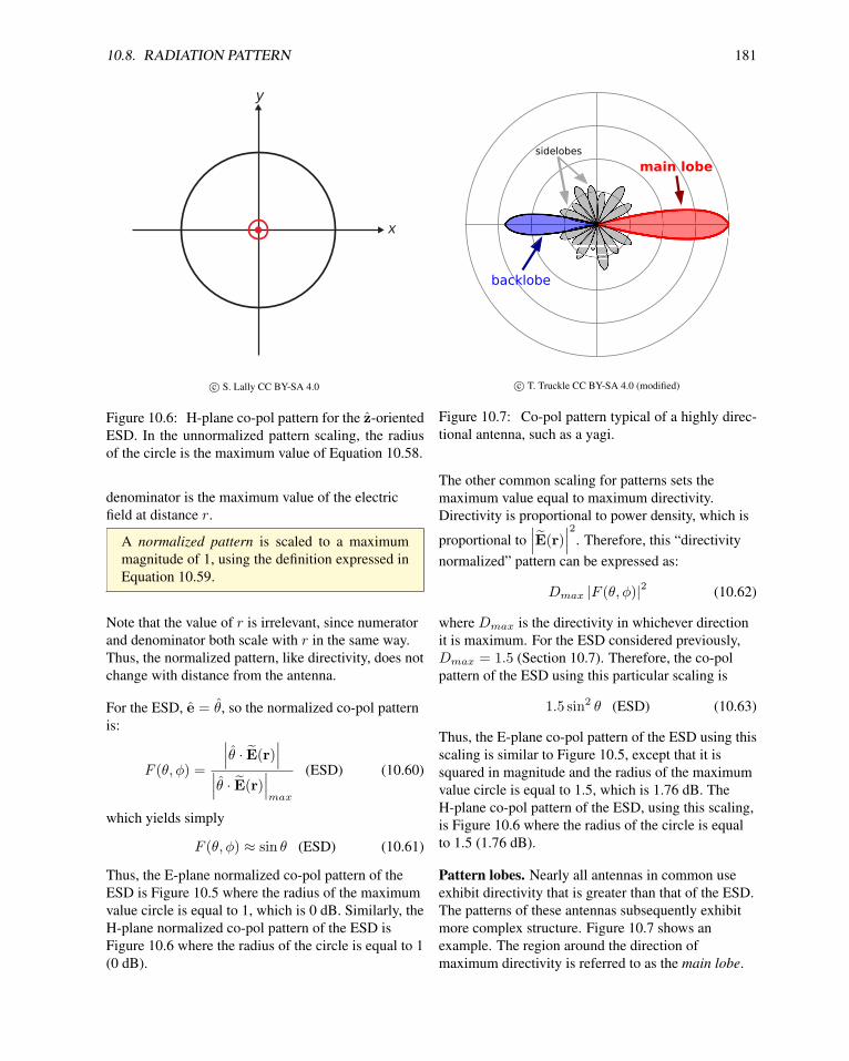
10.8. RADIATION PATTERN 181
c© S. Lally CC BY-SA 4.0
Figure 10.6: H-plane co-pol pattern for the z-oriented
ESD. In the unnormalized pattern scaling, the radius
of the circle is the maximum value of Equation 10.58.
denominator is the maximum value of the electric
field at distance r.
A normalized pattern is scaled to a maximum
magnitude of 1, using the definition expressed in
Equation 10.59.
Note that the value of r is irrelevant, since numerator
and denominator both scale with r in the same way.
Thus, the normalized pattern, like directivity, does not
change with distance from the antenna.
For the ESD, e = θ, so the normalized co-pol pattern
is:
F (θ, φ) =
∣∣∣θ · E(r)∣∣∣
∣∣∣θ · E(r)∣∣∣max
(ESD) (10.60)
which yields simply
F (θ, φ) ≈ sin θ (ESD) (10.61)
Thus, the E-plane normalized co-pol pattern of the
ESD is Figure 10.5 where the radius of the maximum
value circle is equal to 1, which is 0 dB. Similarly, the
H-plane normalized co-pol pattern of the ESD is
Figure 10.6 where the radius of the circle is equal to 1
(0 dB).
c© T. Truckle CC BY-SA 4.0 (modified)
Figure 10.7: Co-pol pattern typical of a highly direc-
tional antenna, such as a yagi.
The other common scaling for patterns sets the
maximum value equal to maximum directivity.
Directivity is proportional to power density, which is
proportional to
∣∣∣E(r)∣∣∣2
. Therefore, this “directivity
normalized” pattern can be expressed as:
Dmax |F (θ, φ)|2 (10.62)
where Dmax is the directivity in whichever direction
it is maximum. For the ESD considered previously,
Dmax = 1.5 (Section 10.7). Therefore, the co-pol
pattern of the ESD using this particular scaling is
1.5 sin2 θ (ESD) (10.63)
Thus, the E-plane co-pol pattern of the ESD using this
scaling is similar to Figure 10.5, except that it is
squared in magnitude and the radius of the maximum
value circle is equal to 1.5, which is 1.76 dB. The
H-plane co-pol pattern of the ESD, using this scaling,
is Figure 10.6 where the radius of the circle is equal
to 1.5 (1.76 dB).
Pattern lobes. Nearly all antennas in common use
exhibit directivity that is greater than that of the ESD.
The patterns of these antennas subsequently exhibit
more complex structure. Figure 10.7 shows an
example. The region around the direction of
maximum directivity is referred to as the main lobe.

182 CHAPTER 10. ANTENNAS
c© S. Lally CC BY-SA 4.0
Figure 10.8: Half-power beamwidth (HPBW).
The main lobe is bounded on each side by a null,
where the magnitude reaches a local minimum,
perhaps zero. Many antennas also exhibit a lobe in
the opposite direction, known as a backlobe. (Many
other antennas exhibit a null in this direction.) Lobes
between the main lobe and the backlobe are referred
to as sidelobes. Other commonly-used pattern metrics
include first sidelobe level, which is the ratio of the
maximum magnitude of the sidelobe closest to the
main lobe to that of the main lobe; and front-to-back
ratio, which is the ratio of the maximum magnitude
of the backlobe to that of the main lobe.
When the main lobe is narrow, it is common to
characterize the pattern in terms of half-power
beamwidth (HPBW). This is shown in Figure 10.8.
HPBW is the width of the main lobe measured
between two points at which the directivity is
one-half its maximum value. As a pattern metric,
HPBW depends on the plane in which it is measured.
In particular, HPBW may be different in the E- and
H-planes. For example, the E-plane HPBW of the
ESD is found to be 90, whereas the H-plane HPBW
is undefined since the pattern is constant in the
H-plane.
Omnidirectional and isotropic antennas. The ESD
is an example of an omnidirectional antenna. An
omnidirectional antenna is an antenna whose pattern
magnitude is nominally constant in a plane containing
the maximum directivity. For the ESD, this plane is
the H-plane, so the ESD is said to be omnidirectional
in the H-plane. The term “omnidirectional” does not
indicate constant pattern in all directions. (In fact,
note that the ESD exhibits pattern nulls in two
directions.)
An omnidirectional antenna, such as the ESD, ex-
hibits constant and nominally maximum directiv-
ity in one plane.
An antenna whose pattern is uniform in all directions
is said to be isotropic. No physically-realizable
antenna is isotropic; in fact, the ESD is about as close
as one can get. Nevertheless, the “isotropic antenna”
concept is useful as a standard against which other
antennas can be quantified. Since the pattern of an
isotropic antenna is constant with direction, the power
density radiated by such an antenna in any direction is
equal to the power density averaged over all
directions. Thus, the directivity of an isotropic
antenna is exactly 1. The directivity of any other
antenna may be expressed in units of “dBi,” which is
simply dB relative to that of an isotropic antenna. For
example, the maximum directivity of the ESD is 1.5,
which is 10 log10 (1.5/1) = 1.76 dBi. Summarizing:
An isotropic antenna exhibits constant directiv-
ity in every direction. Such an antenna is not
physically-realizable, but is nevertheless useful
as a baseline for describing other antennas.
Additional Reading:
• “Radiation pattern” on Wikipedia.

10.9. EQUIVALENT CIRCUIT MODEL FOR RECEPTION 183
10.9 Equivalent Circuit Model
for Reception
[m0206]
In this section, we begin to address antennas as
devices that convert incident electromagnetic waves
into potentials and currents in a circuit. It is
convenient to represent this process in the form of a
Thevenin equivalent circuit. The particular circuit
addressed in this section is shown in Figure 10.9. The
circuit consists of a voltage source VOC and a series
impedance ZA. The source potential VOC is the
potential at the terminals of the antenna when there is
no termination; i.e., when the antenna is
open-circuited. The series impedance ZA is the
output impedance of the circuit, and so determines the
magnitude and phase of the current at the terminals
once a load is connected. Given VOC and the current
through the equivalent circuit, it is possible to
determine the power delivered to the load. Thus, this
model is quite useful, but only if we are able to
determine VOC and ZA. This section provides an
informal derivation of these quantities that is
sufficient to productively address the subsequent
important topics of effective aperture and impedance
matching of receive antennas.3
Vector effective length. With no derivation required,
we can deduce the following about VOC :
• VOC must depend on the incident electric field
3Formal derivations of these quantities are provided in subse-
quent sections. The starting point is the section on reciprocity.
c© S. Lally, CC BY-SA 4.0 (modified)
Figure 10.9: Thevenin equivalent circuit for an an-
tenna in the presence of an incident electromagnetic
wave.
intensity Ei. Presumably the relationship is
linear, so VOC is proportional to the magnitude
of Ei.
• Since Ei is a vector whereas VOC is a scalar,
there must be some vector le for which
VOC = Ei · le (10.64)
• Since Ei has SI base units of V/m and VOC has
SI base units of V, le must have SI base units of
m; i.e., length.
• We expect that VOC increases as the size of the
antenna increases, so the magnitude of le likely
increases with the size of the antenna.
• The direction of le must be related to the
orientation of the incident electric field relative
to that of the antenna, since this is clearly
important yet we have not already accounted for
this.
It may seem at this point that le is unambiguously
determined, and we need merely to derive its value.
However, this is not the case. There are in fact
multiple unique definitions of le that will reduce the
vector Ei to the observed scalar VOC via
Equation 10.64. In this section, we shall employ the
most commonly-used definition, in which le is
referred to as vector effective length. Following this
definition, the scalar part le of le = lle is commonly
referred to as any of the following: effective length
(the term used in this book), effective height, or
antenna factor.
In this section, we shall merely define vector effective
length, and defer a formal derivation to Section 10.11.
In this definition, we arbitrarily set l, the real-valued
unit vector indicating the direction of le, equal to the
direction in which the electric field transmitted from
this antenna would be polarized in the far field. For
example, consider a z-oriented electrically-short
dipole (ESD) located at the origin. The electric field
transmitted from this antenna would have only a θcomponent, and no φ component (and certainly no r
component). Thus, l = θ in this case.
Applying this definition, Ei · l yields the scalar
component of Ei that is co-polarized with electric
field radiated by the antenna when transmitting. Now

184 CHAPTER 10. ANTENNAS
le is uniquely defined to be the factor that converts
this component into VOC . Summarizing:
The vector effective length le = lle is defined
as follows: l is the real-valued unit vector cor-
responding to the polarization of the electric field
that would be transmitted from the antenna in the
far field. Subsequently, the effective length le is
le ,VOC
Ei · l(10.65)
where VOC is the open-circuit potential induced
at the antenna terminals in response to the inci-
dent electric field intensity Ei.
While this definition yields an unambiguous value for
le, it is not yet clear what that value is. For most
antennas, effective length is quite difficult to
determine directly, and one must instead determine
effective length indirectly from the transmit
characteristics via reciprocity. This approach is
relatively easy (although still quite a bit of effort) for
thin dipoles, and is presented in Section 10.11.
To provide an example of how effective length works
right away, consider the z-oriented ESD described
earlier in this section. Let the length of this ESD be
L. Let Ei be a θ-polarized plane wave arriving at the
ESD. The ESD is open-circuited, so the potential
induced in its terminals is VOC . One observes the
following:
• When Ei arrives from anywhere in the θ = π/2
plane (i.e., broadside to the ESD), Ei points in
the −z direction, and we find that le ≈ L/2. It
should not be surprising that le is proportional to
L; this expectation was noted earlier in this
section.
• When Ei arrives from the directions θ = 0 or
θ = π – i.e., along the axis of the ESD – Ei is
perpendicular to the axis of the ESD. In this
case, we find that le equals zero.
Taken together, these findings suggest that le should
contain a factor of sin θ. We conclude that the vector
effective length for a z-directed ESD of length L is
le ≈ θL
2sin θ (ESD) (10.66)
Example 10.7. Potential induced in an ESD.
A thin straight dipole of length 10 cm is located
at the origin and aligned with the z-axis. A plane
wave is incident on the dipole from the direction
(θ = π/4, φ = π/2). The frequency of the wave
is 30 MHz. The magnitude of the incident
electric field is 10 µV/m (rms). What is the
magnitude of the induced open-circuit potential
when the electric field is (a) θ-polarized and (b)
φ-polarized?
Solution. The wavelength in this example is
c/f ∼= 10 m, so this dipole is electrically-short.
Using Equation 10.66:
le ≈ θ10 cm
2sin
π
4
≈ θ (3.54 cm)
Thus, the effective length le = 3.54 cm. When
the electric field is θ-polarized, the magnitude of
the induced open-circuit voltage is
∣∣∣VOC∣∣∣ =
∣∣∣Ei · le∣∣∣
≈ (10 µV/m) θ · θ (3.54 cm)
≈ 354 nV rms (a)
When the electric field is φ-polarized:
∣∣∣VOC∣∣∣ ≈ (10 µV/m) φ · θ (3.54 cm)
≈ 0 (b)
This is because the polarization of the incident
electric field is orthogonal to that of the ESD. In
fact, the answer to part (b) is zero for any angle
of incidence (θ, φ).
Output impedance. The output impedance ZA is
somewhat more difficult to determine without a
formal derivation, which is presented in
Section 10.12. For the purposes of this section, it
suffices to jump directly to the result:
10.9. EQUIVALENT CIRCUIT MODEL FOR RECEPTION 185
The output impedance ZA of the equivalent cir-
cuit for an antenna in the receive case is equal to
the input impedance of the same antenna in the
transmit case.
This remarkable fact is a consequence of the
reciprocity property of antenna systems, and greatly
simplifies the analysis of receive antennas.
Now a demonstration of how the antenna equivalent
circuit can be used to determine the power delivered
by an antenna to an attached electrical circuit:
Example 10.8. Power captured by an ESD.
Continuing with part (a) of Example 10.7: If this
antenna is terminated into a conjugate-matched
load, then what is the power delivered to that
load? Assume the antenna is lossless.
Solution. First, we determine the impedance ZAof the equivalent circuit of the antenna. This is
equal to the input impedance of the antenna in
transmission. Let RA and XA be the real and
imaginary parts of this impedance; i.e.,
ZA = RA + jXA. Further, RA is the sum of the
radiation resistance Rrad and the loss resistance.
The loss resistance is zero because the antenna is
lossless. Since this is an ESD:
Rrad ≈ 20π2
(L
λ
)2
(10.67)
Therefore, RA = Rrad ≈ 4.93 mΩ. We do not
need to calculate XA, as will become apparent
in the next step.
A conjugate-matched load has impedance Z∗A,
so the potential VL across the load is
VL = VOCZ∗A
ZA + Z∗A
= VOCZ∗A
2RA(10.68)
The current IL through the load is
IL =VOC
ZA + Z∗A
=VOC2RA
(10.69)
Taking VOC as an RMS quantity, the power PL
delivered to the load is
PL = Re VLI∗L =
∣∣∣VOC∣∣∣2
4RA(10.70)
In part (a) of Example 10.7,
∣∣∣VOC∣∣∣ is found to be
≈ 354 nV rms, so PL ≈ 6.33 pW.
Additional Reading:
• “Thevenin’s Theorem” on Wikipedia.
• W.L. Stutzman & G.A. Thiele, Antenna Theory
and Design, 3rd Ed., Wiley, 2012. Sec. 4.2
(“Receiving Properties of Antennas”).

186 CHAPTER 10. ANTENNAS
10.10 Reciprocity
[m0214]
The term “reciprocity” refers to a class of theorems
that relate the inputs and outputs of a linear system to
those of an identical system in which the inputs and
outputs are swapped. The importance of reciprocity in
electromagnetics is that it simplifies problems that
would otherwise be relatively difficult to solve. An
example of this is the derivation of the receiving
properties of antennas, which is addressed in other
sections using results derived in this section.
As an initial and relatively gentle introduction,
consider a well-known special case that emerges in
basic circuit theory: The two-port device shown in
Figure 10.10. The two-port is said to be reciprocal if
the voltage v2 appearing at port 2 due to a current
applied at port 1 is the same as v1 when the same
current is applied instead at port 2. This is normally
the case when the two-port consists exclusively of
linear passive devices such as ideal resistors,
capacitors, and inductors. The fundamental
underlying requirement is linearity: That is, outputs
must be proportional to inputs, and superposition
must apply.
This result from basic circuit theory is actually a
special case of a more general theorem of
electromagnetics, which we shall now derive.
Figure 10.11 shows a scenario in which a current
distribution J1 is completely contained within a
volume V . This current is expressed as a volume
current density, having SI base units of A/m2. Also,
the current is expressed in phasor form, signaling that
we are considering a single frequency. This current
distribution gives rise to an electric field intensity E1,
Inductiveload, public domain (modified)
Figure 10.10: Two-port device.
c© C. Wang CC BY-SA 4.0
Figure 10.11: An electromagnetic system consisting
of a current distribution J1 radiating an electric field
E1 in the presence of linear matter.
c© C. Wang CC BY-SA 4.0
Figure 10.12: The same electromagnetic system as
shown in Figure 10.11 (including the same distribution
of matter), but now with a different input, J2, resulting
in a different output, E2.

10.10. RECIPROCITY 187
having SI base units of V/m. The volume may consist
of any combination of linear time-invariant matter;
i.e., permittivity ǫ, permeability µ, and conductivity σare constants that may vary arbitrarily with position
but not with time.
Here’s a key idea: We may interpret this scenario as a
“two-port” system in which J1 is the input, E1 is the
output, and the system’s behavior is completely
defined by Maxwell’s equations in differential phasor
form:
∇× E1 = −jωµH1 (10.71)
∇× H1 = J1 + jωǫE1 (10.72)
along with the appropriate electromagnetic boundary
conditions. (For the purposes of our present analysis,
H1 is neither an input nor an output; it is merely a
coupled quantity that appears in this particular
formulation of the relationship between E1 and J1.)
Figure 10.12 shows a scenario in which a different
current distribution J2 is completely contained within
the same volume V containing the same distribution
of linear matter. This new current distribution gives
rise to an electric field intensity E2. The relationship
between E2 and J2 is governed by the same
equations:
∇× E2 = −jωµH2 (10.73)
∇× H2 = J2 + jωǫE2 (10.74)
along with the same electromagnetic boundary
conditions. Thus, we may interpret this scenario as
the same electromagnetic system depicted in
Figure 10.11, except now with J2 as the input and E2
is the output.
The input current and output field in the second
scenario are, in general, completely different from the
input current and output field in the first scenario.
However, both scenarios involve precisely the same
electromagnetic system; i.e., the same governing
equations and the same distribution of matter. This
leads to the following question: Let’s say you know
nothing about the system, aside from the fact that it is
linear and time-invariant. However, you are able to
observe the first scenario; i.e., you know E1 in
response to J1. Given this very limited look into the
behavior of the system, what can you infer about E2
given J2, or vice-versa? At first glance, the answer
might seem to be nothing, since you lack a description
of the system. However, the answer turns out to be
that a surprising bit more information is available.
This information is provided by reciprocity. To show
this, we must engage in some pure mathematics.
Derivation of the Lorentz reciprocity theorem.
First, let us take the dot product of H2 with each side
of Equation 10.71:
H2 ·(∇× E1
)= −jωµH1 · H2 (10.75)
Similarly, let us take the dot product of E1 with each
side of Equation 10.74:
E1 ·(∇× H2
)= E1 · J2 + jωǫE1 · E2 (10.76)
Next, let us subtract Equation 10.75 from
Equation 10.76. The left side of the resulting equation
is
E1 ·(∇× H2
)− H2 ·
(∇× E1
)(10.77)
This can be simplified using the vector identity
(Appendix B.3):
∇· (A×B) = B · (∇×A)−A · (∇×B) (10.78)
Yielding
E1 ·(∇× H2
)− H2 ·
(∇× E1
)= ∇·
(H2 × E1
)
(10.79)
So, by subtracting Equation 10.75 from
Equation 10.76, we have found:
∇·(H2 × E1
)= E1 · J2+jωǫE1 ·E2+jωµH1 ·H2
(10.80)
Next, we repeat the process represented by
Equations 10.75–10.80 above to generate a
complementary equation to Equation 10.80. This time
we take the dot product of E2 with each side of
Equation 10.72:
E2 ·(∇× H1
)= E2 · J1 + jωǫE1 · E2 (10.81)
Similarly, let us take the dot product of H1 with each
side of Equation 10.73:
H1 ·(∇× E2
)= −jωµH1 · H2 (10.82)
188 CHAPTER 10. ANTENNAS
Next, let us subtract Equation 10.82 from
Equation 10.81. Again using the vector identity, the
left side of the resulting equation is
E2 ·(∇× H1
)− H1 ·
(∇× E2
)= ∇·
(H1 × E2
)
(10.83)
So we find:
∇·(H1 × E2
)= E2 · J1+jωǫE1 ·E2+jωµH1 ·H2
(10.84)
Finally, subtracting Equation 10.84 from
Equation 10.80, we obtain:
∇ ·(H2 × E1 − H1 × E2
)= E1 · J2 − E2 · J1
(10.85)
This equation is commonly known by the name of the
theorem it represents: The Lorentz reciprocity
theorem. The theorem is a very general statement
about the relationship between fields and currents at
each point in space. An associated form of the
theorem applies to contiguous regions of space. To
obtain this form, we simply integrate both sides of
Equation 10.85 over the volume V:
∫
V
∇ ·(H2 × E1 − H1 × E2
)dv
=
∫
V
(E1 · J2 − E2 · J1
)dv (10.86)
We now take the additional step of using the
divergence theorem (Appendix B.3) to transform the
left side of the equation into a surface integral:
∮
S
(H2 × E1 − H1 × E2
)· ds
=
∫
V
(E1 · J2 − E2 · J1
)dv (10.87)
where S is the closed mathematical surface which
bounds V . This is also the Lorentz reciprocity
theorem, but now in integral form. This version of the
theorem relates fields on the bounding surface to
sources within the volume.
The integral form of the theorem has a particularly
useful feature. Let us confine the sources to a finite
region of space, while allowing V to grow infinitely
large, expanding to include all space. In this situation,
the closest distance between any point containing
non-zero source current and S is infinite. Because
field magnitude diminishes with distance from the
source, the fields (E1, H1) and (E2, H2) are all
effectively zero on S . In this case, the left side of
Equation 10.87 is zero, and we find:
∫
V
(E1 · J2 − E2 · J1
)dv = 0 (10.88)
for any volume V which contains all the current.
The Lorentz reciprocity theorem (Equa-
tion 10.88) describes a relationship between
one distribution of current and the resulting
fields, and a second distribution of current and
resulting fields, when both scenarios take place
in identical regions of space filled with identical
distributions of linear matter.
Why do we refer to this relationship as reciprocity?
Simply because the expression is identical when the
subscripts “1” and “2” are swapped. In other words,
the relationship does not recognize a distinction
between “inputs” and “outputs;” there are only
“ports.”
A useful special case pertains to scenarios in which
the current distributions J1 and J2 are spatially
disjoint. By “spatially disjoint,” we mean that there is
no point in space at which both J1 and J2 are
non-zero; in other words, these distributions do not
overlap. (Note that the currents shown in
Figures 10.11 and 10.12 are depicted as spatially
disjoint.) To see what happens in this case, let us first
rewrite Equation 10.88 as follows:
∫
V
E1 · J2 dv =
∫
V
E2 · J1 dv (10.89)
Let V1 be the contiguous volume over which J1 is
non-zero, and let V2 be the contiguous volume over
which J2 is non-zero. Then Equation 10.89 may be
written as follows:
∫
V2
E1 · J2 dv =
∫
V1
E2 · J1 dv (10.90)
The utility of this form is that we have reduced the
region of integration to just those regions where the
current exists.

10.10. RECIPROCITY 189
c© C. Wang CC BY-SA 4.0
Figure 10.13: A two-port consisting of two dipole
antennas.
Reciprocity of two-ports consisting of antennas.
Equation 10.90 allows us to establish the reciprocity
of two-ports consisting of pairs of antennas. This is
most easily demonstrated for pairs of thin dipole
antennas, as shown in Figure 10.13. Here, port 1 is
defined by the terminal quantities (V1, I1) of the
antenna on the left, and port 2 is defined by the
terminal quantities (V2, I2) of the antenna on the
right. These quantities are defined with respect to a
small gap of length ∆l between the
perfectly-conducting arms of the dipole. Either
antenna may transmit or receive, so (V1, I1) depends
on (V2, I2), and vice-versa.
The transmit and receive cases for port 1 are
illustrated in Figure 10.14(a) and (b), respectively.
Note that J1 is the current distribution on this antenna
when transmitting (i.e., when driven by the impressed
current It1) and E2 is the electric field incident on the
antenna when the other antenna is transmitting. Let us
select V1 to be the cylindrical volume defined by the
exterior surface of the dipole, including the gap
between the arms of the dipole. We are now ready to
consider the right side of Equation 10.90:∫
V1
E2 · J1 dv (10.91)
The electromagnetic boundary conditions applicable
to the perfectly-conducting dipole arms allow this
integral to be dramatically simplified. First, recall that
all current associated with a perfect conductor must
flow on the surface of the material, and therefore
c© C. Wang CC BY-SA 4.0
Figure 10.14: The port 1 antenna (a) transmitting and
(b) receiving.
J1 = 0 everywhere except on the surface. Therefore,
the direction of J1 is always tangent to the surface.
The tangent component of E2 is zero on the surface
of a perfectly-conducting material, as required by the
applicable boundary condition. Therefore,
E2 · J1 = 0 everywhere J1 is non-zero.
There is only one location where the current is
non-zero and yet there is no conductor: This location
is the gap located precisely at the terminals. Thus, we
find:∫
V1
E2 · J1 dv =
∫
gap
E2 · It1 l1 dl (10.92)
where the right side is a line integral crossing the gap
that defines the terminals of the antenna. We assume
the current It1 is constant over the gap, and so may be
factored out of the integral:∫
V1
E2 · J1 dv = It1
∫
gap
E2 · l1 dl (10.93)
Recall that potential between two points in space is
given by the integral of the electric field over any path
between those two points. In particular, we may
calculate the open-circuit potential V r1 as follows:
V r1 = −∫
gap
E2 · l1 dl (10.94)
Remarkably, we have found:∫
V1
E2 · J1 dv = −It1V r1 (10.95)

190 CHAPTER 10. ANTENNAS
Applying the exact same procedure for port 2 (or by
simply exchanging subscripts), we find:
∫
V2
E1 · J2 dv = −It2V r2 (10.96)
Now substituting these results into Equation 10.90,
we find:
It1Vr1 = It2V
r2 (10.97)
At the beginning of this section, we stated that a
two-port is reciprocal if V2 appearing at port 2 due to
a current applied at port 1 is the same as V1 when the
same current is applied instead at port 2. If the
present two-dipole problem is reciprocal, then V r2 due
to It1 should be the same as V r1 when It2 = It1. Is it?
Let us set It1 equal to some particular value I0, then
the resulting value of V r2 will be some particular
value V0. If we subsequently set It2 equal to I0, then
the resulting value of V r1 will be, according to
Equation 10.97:
V r1 =It2V
r2
It1=I0V0I0
= V0 (10.98)
Therefore, Equation 10.97 is simply a mathematical
form of the familiar definition of reciprocity from
basic circuit theory, and we have found that our
system of antennas is reciprocal in precisely this same
sense.
The above analysis presumed pairs of straight,
perfectly conducting dipoles of arbitrary length.
However, the result is readily generalized – in fact, is
the same – for any pair of passive antennas in linear
time-invariant media. Summarizing:
The potential induced at the terminals of one an-
tenna due to a current applied to a second antenna
is equal to the potential induced in the second an-
tenna by the same current applied to the first an-
tenna (Equation 10.97).
Additional Reading:
• “Reciprocity (electromagnetism)” on Wikipedia.
• “Two-port network” on Wikipedia.
10.11 Potential Induced in a
Dipole
[m0215]
An electromagnetic wave incident on an antenna will
induce a potential at the terminals of the antenna. In
this section, we shall derive this potential. To simplify
the derivation, we shall consider the special case of a
straight thin dipole of arbitrary length that is
illuminated by a plane wave. However, certain aspects
of the derivation will apply to antennas generally. In
particular, the concepts of effective length (also
known as effective height) and vector effective length
emerge naturally from this derivation, so this section
also serves as a stepping stone in the development of
an equivalent circuit model for a receiving antenna.
The derivation relies on the transmit properties of
dipoles as well as the principle of reciprocity, so
familiarity with those topics is recommended before
reading this section.
The scenario of interest is shown in Figure 10.15.
Here a thin z-aligned straight dipole is located at the
origin. The total length of the dipole is L. The arms
of the dipole are perfectly-conducting. The terminals
consist of a small gap of length ∆l between the arms.
The incident plane wave is described in terms of its
electric field intensity Ei. The question is: What is
VOC , the potential at the terminals when the terminals
are open-circuited?
There are multiple approaches to solve this problem.
A direct attack is to invoke the principle that potential
is equal to the integral of the electric field intensity
over a path. In this case, the path begins at the “−”
terminal and ends at the “+” terminal, crossing the
gap that defines the antenna terminals. Thus:
VOC = −∫
gap
Egap · dl (10.99)
where Egap is the electric field in the gap. The
problem with this approach is that the value of Egap
is not readily available. It is not simply Ei, because
the antenna structure (in particular, the
electromagnetic boundary conditions) modify the
electric field in the vicinity of the antenna.4
4Also, if this were true, then the antenna itself would not matter;

10.11. POTENTIAL INDUCED IN A DIPOLE 191
Fortunately, we can bypass this obstacle using the
principle of reciprocity. In a reciprocity-based
strategy, we establish a relationship between two
scenarios that take place within the same
electromagnetic system. The first scenario is shown in
Figure 10.16. In this scenario, we have two dipoles.
The first dipole is precisely the dipole of interest
(Figure 10.15), except that a current It1 is applied to
the antenna terminals. This gives rise to a current
distribution I(z) (SI base units of A) along the dipole,
and subsequently the dipole radiates the electric field
(Section 9.6):
E1(r) ≈ θjη
2
e−jβr
r(sin θ)
·[1
λ
∫ +L/2
−L/2
I(z′)e+jβz′ cos θdz′
](10.100)
The second antenna is a θ-aligned Hertzian dipole in
the far field, which receives E1. (For a refresher on
the properties of Hertzian dipoles, see Section 9.4. A
key point is that Hertzian dipoles are vanishingly
small.) Specifically, we measure (conceptually, at
least) the open-circuit potential V r2 at the terminals of
the Hertzian dipole. We select a Hertzian dipole for
this purpose because – in contrast to essentially all
only the relative spacing and orientation of the antenna terminals
would matter!
c© C. Wang CC BY-SA 4.0
Figure 10.15: A potential is induced at the terminals
of a thin straight dipole in response to an incident plane
wave.
c© C. Wang CC BY-SA 4.0
Figure 10.16: The dipole of interest driven by current
It1 radiates electric field E1, resulting in open-circuit
potential V r2 at the terminals of a Hertzian dipole in
the far field.
c© C. Wang CC BY-SA 4.0
Figure 10.17: The Hertzian dipole driven by current
It2 radiates electric field E2, resulting in open-circuit
potential V r1 at the terminals of the dipole of interest.
192 CHAPTER 10. ANTENNAS
other antennas – it is simple to determine the open
circuit potential. As explained earlier:
V r2 = −∫
gap
Egap · dl (10.101)
For the Hertzian dipole, Egap is simply the incident
electric field, since there is negligible structure (in
particular, a negligible amount of material) present to
modify the electric field. Thus, we have simply:
V r2 = −∫
gap
E1 · dl (10.102)
Since the Hertzian dipole is very short and very far
away from the transmitting dipole, E1 is essentially
constant over the gap. Also recall that we required the
Hertzian dipole to be aligned with E1. Choosing to
integrate in a straight line across the gap,
Equation 10.102 reduces to:
V r2 = −E1(r2) · θ∆l (10.103)
where ∆l is the length of the gap and r2 is the
location of the Hertzian dipole. Substituting the
expression for E1 from Equation 10.100, we obtain:
V r2 ≈− jη
2
e−jβr2
r2(sin θ)
·[1
λ
∫ +L/2
−L/2
I(z′)e+jβz′ cos θdz′
]∆l
(10.104)
where r2 = |r2|.
The second scenario is shown in Figure 10.17. This
scenario is identical to the first scenario, with the
exception that the Hertzian dipole transmits and the
dipole of interest receives. The field radiated by the
Hertzian dipole in response to applied current It2,
evaluated at the origin, is (Section 9.4):
E2(r = 0) ≈ θjηIt2 · β∆l
4π(1)
e−jβr2
r2(10.105)
The “sin θ” factor in the general expression is equal to
1 in this case, since, as shown in Figure 10.17, the
origin is located broadside (i.e., at π/2 rad) relative to
the axis of the Hertzian dipole. Also note that because
the Hertzian dipole is presumed to be in the far field,
E2 may be interpreted as a plane wave in the region
of the receiving dipole of interest.
Now we ask: What is the induced potential V r1 in the
dipole of interest? Once again, Equation 10.99 is not
much help, because the electric field in the gap is not
known. However, we do know that V r1 should be
proportional to E2(r = 0), since this is presumed to
be a linear system. Based on this much information
alone, there must be some vector le = lle for which
V r1 = E2(r = 0) · le (10.106)
This does not uniquely define either the unit vector l
nor the scalar part le, since a change in the definition
of the former can be compensated by a change in the
definition of the latter and vice-versa. So at this point
we invoke the standard definition of le as the vector
effective length, introduced in Section 10.9. Thus, l is
defined to be the direction in which an electric field
transmitted from the antenna would be polarized. In
the present example, l = −θ, where the minus sign
reflects the fact that positive terminal potential results
in terminal current which flows in the −z direction.
Thus, Equation 10.106 becomes:
V r1 = −E2(r = 0) · θle (10.107)
We may go a bit further and substitute the expression
for E2(r = 0) from Equation 10.105:
V r1 ≈ −jη It2 · β∆l4π
e−jβr2
r2le (10.108)
Now we invoke reciprocity. As a two-port linear
time-invariant system, it must be true that:
It1Vr1 = It2V
r2 (10.109)
Thus:
V r1 =It2
It1V r2 (10.110)
Substituting the expression for V r2 from
Equation 10.104:
V r1 ≈− It2
It1· j η
2
e−jβr2
r2(sin θ)
·[1
λ
∫ +L/2
−L/2
I(z′)e+jβz′ cos θdz′
]∆l
(10.111)
Thus, reciprocity has provided a second expression
for V r1 . We may solve for le by setting this expression

10.11. POTENTIAL INDUCED IN A DIPOLE 193
equal to the expression from Equation 10.108,
yielding
le ≈2π
βIt1
[1
λ
∫ +L/2
−L/2
I(z′)e+jβz′ cos θdz′
]sin θ
(10.112)
Noting that β = 2π/λ, this simplifies to:
le ≈[1
It1
∫ +L/2
−L/2
I(z′)e+jβz′ cos θdz′
]sin θ
(10.113)
Thus, you can calculate le using the following
procedure:
1. Apply a current It1 to the dipole of interest.
2. Determine the resulting current distribution I(z)along the length of the dipole. (Note that
precisely this is done for the electrically-short
dipole in Section 9.5 and for the half-wave
dipole in Section 9.7.)
3. Integrate I(z) over the length of the dipole as
indicated in Equation 10.113. Then divide
(“normalize”) by It1 (which is simply I(0)). Note
that the result is independent of the excitation It1,
as expected since this is a linear system.
4. Multiply by sin θ.
We have now determined that the open-circuit
terminal potential VOC in response to an incident
electric field Ei is
VOC = Ei · le (10.114)
where le = lle is the vector effective length defined
previously.
This result is remarkable. In plain English, we have
found that:
The potential induced in a dipole is the co-
polarized component of the incident electric field
times a normalized integral of the transmit cur-
rent distribution over the length of the dipole,
times sine of the angle between the dipole axis
and the direction of incidence.
In other words, the reciprocity property of linear
systems allows this property of a receiving antenna to
be determined relatively easily if the transmit
characteristics of the antenna are known.
Example 10.9. Effective length of a thin
electrically-short dipole (ESD).
A explained in Section 9.5, the current
distribution on a thin ESD is
I(z) ≈ I0
(1− 2
L|z|)
(10.115)
where L is the length of the dipole and I0 is the
terminal current. Applying Equation 10.113, we
find:
le ≈[1
I0
∫ +L/2
−L/2
I0
(1− 2
L|z′|)e+jβz
′ cos θdz′
]
· sin θ (10.116)
Recall β = 2π/λ, so βz′ = 2π (z′/λ). Since
this is an electrically-short dipole, z′ ≪ λ over
the entire integral, and subsequently we may
assume e+jβz′ cos θ ≈ 1 over the entire integral.
Thus:
le ≈[∫ +L/2
−L/2
(1− 2
L|z′|)dz′
]sin θ
(10.117)
The integral is easily solved using standard
methods, or simply recognize that the “area
under the curve” in this case is simply one-half
“base” (L) times “height” (1). Either way, we
find
le ≈L
2sin θ (10.118)
Example 10.7 (Section 10.9) demonstrates how
Equation 10.114 with the vector effective length
determined in the preceding example is used to obtain
the induced potential.

194 CHAPTER 10. ANTENNAS
10.12 Equivalent Circuit Model
for Reception, Redux
[m0216]
Section 10.9 provides an informal derivation of an
equivalent circuit model for a receiving antenna. This
model is shown in Figure 10.18. The derivation of
this model was informal and incomplete because the
open-circuit potential Ei · le and source impedance
ZA were not rigorously derived in that section. While
the open-circuit potential was derived in
Section 10.11 (“Potential Induced in a Dipole”), the
source impedance has not yet been addressed. In this
section, the source impedance is derived, which
completes the formal derivation of the model. Before
reading this section, a review of Section 10.10
(“Reciprocity”) is recommended.
The starting point for a formal derivation is the
two-port model shown in Figure 10.19. If the
two-port is passive, linear, and time-invariant, then
the potential v2 is a linear function of potentials and
currents present at ports 1 and 2. Furthermore, v1must be proportional to i1, and similarly v2 must be
proportional to i2, so any pair of “inputs” consisting
of either potentials or currents completely determines
the two remaining potentials or currents. Thus, we
may write:
v2 = Z21i1 + Z22i2 (10.119)
where Z11 and Z12 are, for the moment, simply
constants of proportionality. However, note that Z11
and Z12 have SI base units of Ω, and so we refer to
c© S. Lally CC BY-SA 4.0
Figure 10.18: Thevenin equivalent circuit model for
an antenna in the presence of an incident electric field
Ei.
Inductiveload, public domain (modified)
Figure 10.19: Two-port system.
these quantities as impedances. Similarly we may
write:
v1 = Z11i1 + Z12i2 (10.120)
We can develop expressions for Z12 and Z21 as
follows. First, note that v1 = Z12i2 when i1 = 0.
Therefore, we may define Z12 as follows:
Z12 ,v1i2
∣∣∣∣i1=0
(10.121)
The simplest way to make i1 = 0 (leaving i2 as the
sole “input”) is to leave port 1 open-circuited. In
previous sections, we invoked special notation for
these circumstances. In particular, we defined It2 as i2in phasor representation, with the superscript “t”(“transmitter”) indicating that this is the sole “input”;
and V r1 as v1 in phasor representation, with the
superscript “r” (“receiver”) signaling that port 1 is
both open-circuited and the “output.” Applying this
notation, we note:
Z12 =V r1
It2(10.122)
Similarly:
Z21 =V r2
It1(10.123)
In Section 10.10 (“Reciprocity”), we established that
a pair of antennas could be represented as a passive
linear time-invariant two-port, with v1 and i1representing the potential and current at the terminals
of one antenna (“antenna 1”), and v2 and i2representing the potential and current at the terminals
of another antenna (“antenna 2”). Therefore for any
pair of antennas, quantities Z11, Z12, Z22, and Z21
10.12. EQUIVALENT CIRCUIT MODEL FOR RECEPTION, REDUX 195
can be identified that completely determine the
relationship between the port potentials and currents.
We also established in Section 10.10 that:
It1Vr1 = It2V
r2 (10.124)
Therefore,
V r1
It2=V r2
It1(10.125)
Referring to Equations 10.122 and 10.123, we see
that Equation 10.125 requires that:
Z12 = Z21 (10.126)
This is a key point. Even though we derived this
equality by open-circuiting ports one at a time, the
equality must hold generally since Equations 10.119
and 10.120 must apply – with the same values of Z12
and Z21 – regardless of the particular values of the
port potentials and currents.
We are now ready to determine the Thevenin
equivalent circuit for a receiving antenna. Let port 1
correspond to the transmitting antenna; that is, i1 is
It1. Let port 2 correspond to an open-circuited
receiving antenna; thus, i2 = 0 and v2 is V r2 . Now
applying Equation 10.119:
v2 = Z21i1 + Z22i2
=(V r2 /I
t1
)It1 + Z22 · 0
= V r2 (10.127)
We previously determined V r2 from electromagnetic
considerations to be (Section 10.11):
V r2 = Ei · le (10.128)
where Ei is the field incident on the receiving
antenna, and le is the vector effective length as
defined in Section 10.11. Thus, the voltage source in
the Thevenin equivalent circuit for the receive
antenna is simply Ei · le, as shown in Figure 10.18.
The other component in the Thevenin equivalent
circuit is the series impedance. From basic circuit
theory, this impedance is the ratio of v2 when port 2 is
open-circuited (i.e., V r2 ) to i2 when port 2 is
short-circuited. This value of i2 can be obtained using
Equation 10.119 with v2 = 0:
0 = Z21It1 + Z22i2 (10.129)
Therefore:
i2 = −Z21
Z22It1 (10.130)
Now using Equation 10.123 to eliminate It1, we
obtain:
i2 = − V r2Z22
(10.131)
Note that the reference direction for i2 as defined in
Figure 10.19 is opposite the reference direction for
short-circuit current. That is, given the polarity of v2shown in Figure 10.19, the reference direction of
current flow through a passive load attached to this
port is from “+” to “−” through the load. Therefore,
the source impedance, calculated as the ratio of the
open-circuit potential to the short circuit current, is:
V r2
+V r2 /Z22
= Z22 (10.132)
We have found that the series impedance ZA in the
Thevenin equivalent circuit is equal to Z22 in the
two-port model.
To determine Z22, let us apply a current i2 = It2 to
port 2 (i.e., antenna 2). Equation 10.119 indicates that
we should see:
v2 = Z21i1 + Z22It2 (10.133)
Solving for Z22:
Z22 =v2
It2− Z21
i1
It2(10.134)
Note that the first term on the right is precisely the
impedance of antenna 2 in transmission. The second
term in Equation 10.134 describes a contribution to
Z22 from antenna 1. However, our immediate interest
is in the equivalent circuit for reception of an electric
field Ei in the absence of any other antenna. We can
have it both ways by imagining that Ei is generated
by antenna 1, but also that antenna 1 is far enough
away to make Z21 – the factor that determines the
effect of antenna 1 on antenna 2 – negligible. Then
we see from Equation 10.134 that Z22 is the
impedance of antenna 2 when transmitting.
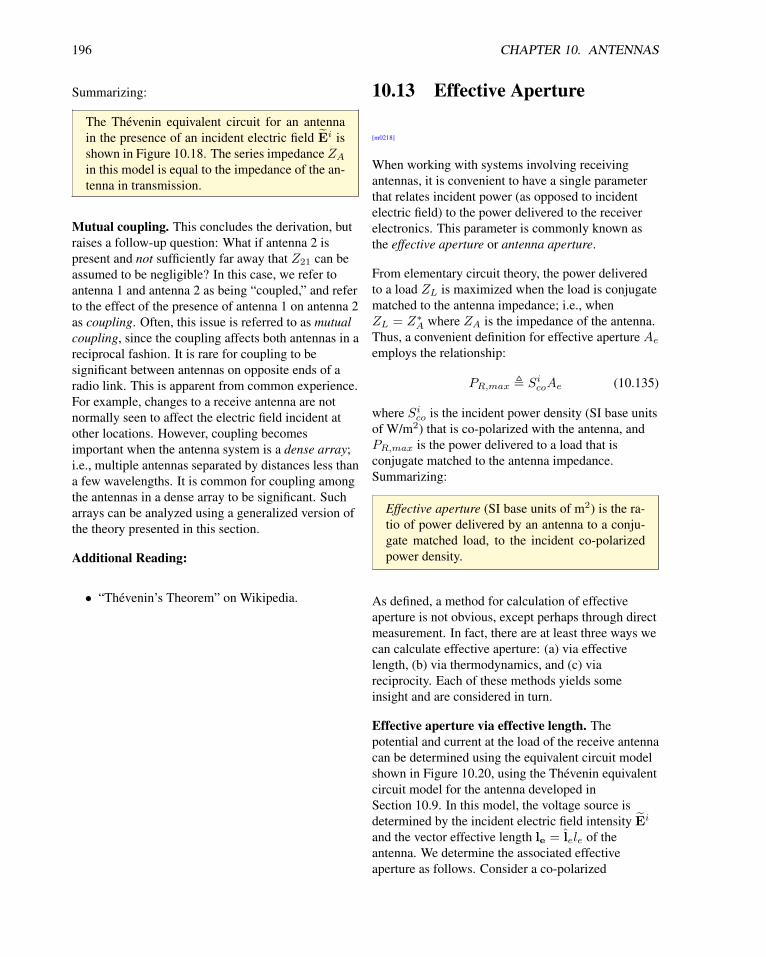
196 CHAPTER 10. ANTENNAS
Summarizing:
The Thevenin equivalent circuit for an antenna
in the presence of an incident electric field Ei is
shown in Figure 10.18. The series impedance ZAin this model is equal to the impedance of the an-
tenna in transmission.
Mutual coupling. This concludes the derivation, but
raises a follow-up question: What if antenna 2 is
present and not sufficiently far away that Z21 can be
assumed to be negligible? In this case, we refer to
antenna 1 and antenna 2 as being “coupled,” and refer
to the effect of the presence of antenna 1 on antenna 2
as coupling. Often, this issue is referred to as mutual
coupling, since the coupling affects both antennas in a
reciprocal fashion. It is rare for coupling to be
significant between antennas on opposite ends of a
radio link. This is apparent from common experience.
For example, changes to a receive antenna are not
normally seen to affect the electric field incident at
other locations. However, coupling becomes
important when the antenna system is a dense array;
i.e., multiple antennas separated by distances less than
a few wavelengths. It is common for coupling among
the antennas in a dense array to be significant. Such
arrays can be analyzed using a generalized version of
the theory presented in this section.
Additional Reading:
• “Thevenin’s Theorem” on Wikipedia.
10.13 Effective Aperture
[m0218]
When working with systems involving receiving
antennas, it is convenient to have a single parameter
that relates incident power (as opposed to incident
electric field) to the power delivered to the receiver
electronics. This parameter is commonly known as
the effective aperture or antenna aperture.
From elementary circuit theory, the power delivered
to a load ZL is maximized when the load is conjugate
matched to the antenna impedance; i.e., when
ZL = Z∗A where ZA is the impedance of the antenna.
Thus, a convenient definition for effective aperture Aeemploys the relationship:
PR,max , SicoAe (10.135)
where Sico is the incident power density (SI base units
of W/m2) that is co-polarized with the antenna, and
PR,max is the power delivered to a load that is
conjugate matched to the antenna impedance.
Summarizing:
Effective aperture (SI base units of m2) is the ra-
tio of power delivered by an antenna to a conju-
gate matched load, to the incident co-polarized
power density.
As defined, a method for calculation of effective
aperture is not obvious, except perhaps through direct
measurement. In fact, there are at least three ways we
can calculate effective aperture: (a) via effective
length, (b) via thermodynamics, and (c) via
reciprocity. Each of these methods yields some
insight and are considered in turn.
Effective aperture via effective length. The
potential and current at the load of the receive antenna
can be determined using the equivalent circuit model
shown in Figure 10.20, using the Thevenin equivalent
circuit model for the antenna developed in
Section 10.9. In this model, the voltage source is
determined by the incident electric field intensity Ei
and the vector effective length le = lele of the
antenna. We determine the associated effective
aperture as follows. Consider a co-polarized
10.13. EFFECTIVE APERTURE 197
sinusoidally-varying plane wave Eico incident on the
antenna. Further, let
Eico = Eie (10.136)
where e is the reference direction of Eico. The
co-polarized power density incident on the antenna is:
Sico =
∣∣Ei∣∣2
2η(10.137)
where η is the wave impedance of the medium (e.g.,∼= 377 Ω for an antenna in free space). In response,
the time-average power delivered to the load is
PR =1
2ReVLI
∗L
(10.138)
where VL and IL are the potential and current
phasors, respectively, at the load. We may determine
VL and IL from the equivalent circuit model of
Figure 10.20 using basic circuit theory. First, note
that the magnitude and phase of the voltage source is:
Eico · le = Eile
(e · le
)(10.139)
and since we have defined le to be equal to e,
Eico · le = Eile (10.140)
Next, note that the load impedance creates a voltage
divider with the source (antenna) impedance such that
VL =(Eile
) ZLZA + ZL
(10.141)
c© S. Lally CC BY-SA 4.0 (modified)
Figure 10.20: Equivalent circuit model for an antenna
in the presence of an incident electric field Ei, termi-
nated into a load impedance ZL.
Similarly, IL is the voltage source output divided by
the total series resistance:
IL =Eile
ZA + ZL(10.142)
Substituting these expressions into Equation 10.138,
we obtain:
PR =1
2
∣∣Eile∣∣2 RL
|ZA + ZL|2(10.143)
Let us identify the real and imaginary components of
ZA and ZL explicitly, as follows:
ZA = RA + jXA (10.144)
ZL = RL + jXL (10.145)
Further, let us assume that loss internal to the antenna
is negligible, so RA ≈ Rrad. If ZL is conjugate
matched for maximum power transfer, then
ZL = Z∗A = Rrad − jXA. Therefore:
PR,max =1
2
∣∣Eile∣∣2 Rrad
|ZA + Z∗A|
2
=1
2
∣∣Eile∣∣2 Rrad
|2Rrad|2
=
∣∣Eile∣∣2
8Rrad(10.146)
Now using Equations 10.135, 10.137, and 10.146, we
find:
Ae =
∣∣Eile∣∣2 /8Rrad
|Ei|2 /2η(10.147)
which reduces to:
Ae =η |le|24Rrad
(10.148)
It is not surprising that effective aperture should be
proportional to the square of the magnitude of
effective length. However, we see that the medium
and the radiation resistance of the antenna also play a
role.
Effective length and radiation resistance are easy to
calculate for wire antennas, so it is natural to use
Equation 10.148 to calculate the effective apertures of

198 CHAPTER 10. ANTENNAS
wire antennas. For the electrically-short dipole (ESD)
of length L, le ≈ (L/2) sin θ and
Rrad ≈ 20π2 (L/λ)2. Thus, we find the effective
aperture assuming free space (i.e., η = η0) is:
Ae ≈ 0.119λ2 |sin θ|2 (lossless ESD) (10.149)
Remarkably, the effective aperture of the ESD does
not depend on its length. In fact, it depends only on
the frequency of operation.
Also worth noting is that maximum effective aperture
(i.e., the effective aperture in the θ = π/2 direction) is
Ae ≈ 0.119λ2 (lossless ESD, max.) (10.150)
Dipoles which are not electrically-short exhibit
radiation resistance which is proportional to Lp,
where p > 2. Therefore, the effective aperture of
non-electrically-short dipoles does increase with L, as
expected. However, this increase is not dramatic
unless L is significantly greater than λ/2. Here’s an
example:
Example 10.10. Effective aperture of a
half-wave dipole.
The electrically-thin half-wave dipole exhibits
radiation resistance ∼= 73 Ω and effective length
λ/π. Assuming the dipole is lossless and in free
space, Equation 10.148 yields:
Ae ≈ 0.131λ2 (half-wave dipole, max.)
(10.151)
Again, this is the effective aperture for a wave
incident from broadside to the dipole.
Effective aperture via thermodynamics. A useful
insight into the concept of effective aperture can be
deduced by asking the following question: How much
power is received by an antenna when waves of equal
power density arrive from all directions
simultaneously? This question is surprisingly easy to
answer using basic principles of thermodynamics.
Thermodynamics is a field of physics that addresses
heat and its relation to radiation and electrical energy.
No previous experience with thermodynamics is
assumed in this derivation.
Consider the scenario depicted in Figure 10.21. In
this scenario, the antenna is completely enclosed in a
chamber whose walls do not affect the behavior of the
antenna and which have uniform temperature T . The
load (still conjugate matched to the antenna) is
completely enclosed by a separate but identical
chamber, also at temperature T .
Consider the load chamber first. Heat causes random
acceleration of constituent charge carriers in the load,
giving rise to a randomly-varying current at the load
terminals. (This is known as Johnson-Nyquist noise.)
This current, flowing through the load, gives rise to a
potential; therefore, the load – despite being a passive
device – is actually a source of power. The power
associated with this noise is:
Pload = kTB (10.152)
where k ∼= 1.38× 10⁻²³ J/K is Boltzmann’s constant
and B is the bandwidth within which Pload is
measured.
Similarly, the antenna is a source of noise power
Pant. Pant can also be interpreted as captured
thermal radiation – that is, electromagnetic waves
stimulated by the random acceleration of charged
particles comprising the chamber walls. These waves
radiate from the walls and travel to the antenna. The
Rayleigh-Jeans law of thermodynamics tells us that
this radiation should have power density (i.e., SI base
units of W/m2) equal to
2kT
λ2B (10.153)
Chetvorno, public domain (modified)
Figure 10.21: Thermodynamic analysis of the power
exchanged between an antenna and its load.

10.13. EFFECTIVE APERTURE 199
per steradian of solid angle.5 The total power
accessible to the antenna is one-half this amount,
since an antenna is sensitive to only one polarization
at a time, whereas the thermal radiation is equally
distributed among any two orthogonal polarizations.
PA is the remaining power, obtained by integrating
over all 4π steradians. Therefore, the antenna
captures total power equal to6
Pant =
∮Ae(θ
′, φ′)
(1
2
2kT
λ2B
)sin θ′dθ′dφ′
=
(kT
λ2B
)∮Ae(θ
′, φ′) sin θ′dθ′dφ′
(10.154)
Given the conditions of the experiment, and in
particular since the antenna chamber and the load
chamber are at the same temperature, the antenna and
load are in thermodynamic equilibrium. A
consequence of this equilibrium is that power Pantcaptured by the antenna and delivered to the load
must be equal to power Pload generated by the load
and delivered to the antenna; i.e.,
Pant = Pload (10.155)
Combining Equations 10.152, 10.154, and 10.155, we
obtain:(kT
λ2B
)∮Ae(θ
′, φ′) sin θ′dθ′dφ′ = kTB
(10.156)
which reduces to:∮Ae(θ
′, φ′) sin θ′dθ′dφ′ = λ2 (10.157)
Let 〈Ae〉 be the mean effective aperture of the
antenna; i.e., Ae averaged over all possible directions.
This average is simply Equation 10.157 divided by
the 4π sr of solid angle comprising all possible
directions. Thus:
〈Ae〉 =λ2
4π(10.158)
Recall that a isotropic antenna is one which has the
same effective aperture in every direction. Such
5Full disclosure: This is an approximation to the exact expres-
sion, but is very accurate at radio frequencies. See “Additional Read-
ing” at the end of this section for additional details.6Recall sin θ′dθ′dφ′ is the differential element of solid angle.
antennas do not exist in practice, but the concept of an
isotropic antenna is quite useful as we shall soon see.
Since the effective aperture of an isotropic antenna
must be the same as its mean effective aperture, we
find:
Ae =λ2
4π≈ 0.080λ2 (isotropic antenna)
(10.159)
Note further that this must be the minimum possible
value of the maximum effective aperture for any
antenna.
Effective aperture via reciprocity. The fact that all
antennas have maximum effective aperture greater
than that of an isotropic antenna makes the isotropic
antenna a logical benchmark against which to
compare the effective aperture of antennas. We can
characterize the effective aperture of any antenna as
being some unitless real-valued constant D times the
effective aperture of an isotropic antenna; i.e.:
Ae , Dλ2
4π(any antenna) (10.160)
where D must be greater than or equal to 1.
Astute readers might notice that D seems a lot like
directivity. Directivity is defined in Section 10.7 as
the factor by which a transmitting antenna increases
the power density of its radiation over that of an
isotropic antenna. Let us once again consider the
ESD, for which we previously determined (via the
effective length concept) that Ae ∼= 0.119λ2 in the
direction in which it is maximum. Applying
Equation 10.160 to the ESD, we find:
D , Ae4π
λ2∼= 1.50 (ESD, max.) (10.161)
Sure enough, D is equal to the directivity of the ESD
in the transmit case.
This result turns out to be generally true; that is:
The effective aperture of any antenna is given by
Equation 10.160 where D is the directivity of the
antenna when transmitting.
A derivation of this result for the general case is
possible using analysis similar to the thermodynamics

200 CHAPTER 10. ANTENNAS
presented earlier, or using the reciprocity theorem
developed in Section 10.10.
The fact that effective aperture is easily calculated
from transmit directivity is an enormously useful tool
in antenna engineering. Without this tool,
determination of effective aperture is limited to direct
measurement or calculation via effective length; and
effective length is generally difficult to calculate for
antennas which are not well-described as distributions
of current along a line. It is usually far easier to
calculate the directivity of an antenna when
transmitting, and then use Equation 10.160 to obtain
effective aperture for receive operation.
Note that this principle is itself an expression of
reciprocity. That is, one may fairly say that
“directivity” is not exclusively a transmit concept nor
a receive concept, but rather is a single quantifiable
characteristic of an antenna that applies in both the
transmit and receive case. Recall that radiation
patterns are used to quantify the way (transmit)
directivity varies with direction. Suddenly, we have
found that precisely the same patterns apply to the
receive case! Summarizing:
As long as the conditions required for formal
reciprocity are satisfied, the directivity of a re-
ceiving antenna (defined via Equation 10.160) is
equal to directivity of the same antenna when
transmitting, and patterns describing receive di-
rectivity are equal to those for transmit directiv-
ity.
Finally, we note that the equivalence of transmit and
receive directivity can, again via Equation 10.160, be
used to define an effective aperture for the transmit
case. In other words, we can define the effective
aperture of a transmitting antenna to be λ2/4π times
the directivity of the antenna. There is no new physics
at work here; we are simply taking advantage of the
fact that the concepts of effective aperture and
directivity describe essentially the same characteristic
of an antenna, and that this characteristic is the same
for both transmit and receive operation.
Additional Reading:
• “Antenna aperture” on Wikipedia.
• “Boltzmann constant” on Wikipedia.
• “Rayleigh-Jeans law” on Wikipedia.
• “Johnson-Nyquist noise” on Wikipedia.
• “Thermodynamics” on Wikipedia.

10.14. FRIIS TRANSMISSION EQUATION 201
10.14 Friis Transmission
Equation
[m0219]
A common task in radio systems applications is to
determine the power delivered to a receiver due to a
distant transmitter. The scenario is shown in
Figure 10.22: A transmitter delivers power PT to an
antenna which has gain GT in the direction of the
receiver. The receiver’s antenna has gain GR. As
always, antenna gain is equal to directivity times
radiation efficiency, so GT and GR account for losses
internal to the antenna, but not losses due to
impedance mismatch.
A simple expression for PR can be derived as follows.
First, let us assume “free space conditions”; that is, let
us assume that the intervening terrain exhibits
negligible absorption, reflection, or other scattering of
the transmitted signal. In this case, the spatial power
density at range R from the transmitter which radiates
this power through a lossless and isotropic antenna
would be:PT
4πR2(10.162)
that is, total transmitted power divided by the area of
a sphere of radius R through which all the power
must flow. The actual power density Si is this amount
times the gain of the transmit antenna, i.e.:
Si =PT
4πR2GT (10.163)
The maximum received power is the incident
co-polarized power density times the effective
Figure 10.22: Radio link accounting for antenna gains
and spreading of the transmitted wave.
aperture Ae of the receive antenna:
PR,max = AeSico
= AePT
4πR2GT (10.164)
This assumes that the receive antenna is co-polarized
with the incident electric field, and that the receiver is
conjugate-matched to the antenna. The effective
aperture can also be expressed in terms of the gain
GR of the receive antenna:
Ae =λ2
4πGR (10.165)
Thus, Equation 10.164 may be written in the
following form:
PR,max = PTGT
(λ
4πR
)2
GR (10.166)
This is the Friis transmission equation. Summarizing:
The Friis transmission equation (Equa-
tion 10.166) gives the power delivered to a
conjugate-matched receiver in response to a dis-
tant transmitter, assuming co-polarized antennas
and free space conditions.
The factor (λ/4πR)2
appearing in the Friis
transmission equation is referred to as free space path
gain. More often this is expressed as the reciprocal
quantity:
Lp ,
(λ
4πR
)−2
(10.167)
which is known as free space path loss. Thus,
Equation 10.166 may be expressed as follows:
PR,max = PTGTL−1p GR (10.168)
The utility of the concept of path loss is that it may
also be determined for conditions which are different
from free space. The Friis transmission equation still
applies; one simply uses the appropriate (and
probably significantly different) value of Lp.
A common misconception is that path loss is equal to
the reduction in power density due to spreading along

202 CHAPTER 10. ANTENNAS
the path between antennas, and therefore this
“spreading loss” increases with frequency. In fact, the
reduction in power density due to spreading between
any two distances R1 < R2 is:
PT /4πR21
PT /4πR22
=
(R1
R2
)2
(10.169)
which is clearly independent of frequency. The path
loss Lp, in contrast, depends only on the total distance
R and does depend on frequency. The dependence on
frequency reflects the dependence of the effective
aperture on wavelength. Thus, path loss is not loss in
the traditional sense, but rather accounts for a
combination of spreading and the λ2 dependence of
effective aperture that is common to all receiving
antennas.
Finally, note that Equation 10.168 is merely the
simplest form of the Friis transmission equation.
Commonly encountered alternative forms include
forms in which GT and/or GR are instead represented
by the associated effective apertures, and forms in
which the effects of antenna impedance mismatch
and/or cross-polarization are taken into account.
Example 10.11. 6 GHz point-to-point link.
Terrestrial telecommunications systems
commonly aggregate large numbers of
individual communications links into a single
high-bandwidth link. This is often implemented
as a radio link between dish-type antennas
having gain of about 27 dBi (that’s dB relative to
a lossless isotropic antenna) mounted on very
tall towers and operating at frequencies around 6
GHz. Assuming the minimum acceptable
receive power is −120 dBm (that’s −120 dB
relative to 1 mW; i.e., 10−15 W) and the
required range is 30 km, what is the minimum
acceptable transmit power?
Solution. From the problem statement:
GT = GR = 1027/10 ∼= 501 (10.170)
λ =c
f∼= 3× 10⁸ m/s
6× 10⁹ Hz∼= 5.00 cm (10.171)
R = 30 km, and PR ≥ 10−15 W. We assume
that the height and high directivity of the
antennas yield conditions sufficiently close to
free space. We further assume
conjugate-matching at the receiver, and that the
antennas are co-polarized. Under these
conditions, PR = PR,max and Equation 10.166
applies. We find:
PT ≥ PR,max
GT (λ/4πR)2GR
(10.172)
∼= 2.26× 10⁻⁷ W
∼= 2.26× 10⁻⁴ mW
∼= −36.5 dBm
Additional Reading:
• “Free-space path loss” on Wikipedia.
• “Friis transmission equation” on Wikipedia.
[m0211]

10.14. FRIIS TRANSMISSION EQUATION 203
Image Credits
Fig. 10.1: c© Offaperry (S. Lally), https://commons.wikimedia.org/wiki/File:Standing Wave Creation.svg,
CC BY-SA 4.0 (https://creativecommons.org/licenses/by-sa/4.0/).
Fig. 10.2: c© Offaperry (S. Lally), https://commons.wikimedia.org/wiki/File:Electrically-Short Dipole.svg,
CC BY-SA 4.0 (https://creativecommons.org/licenses/by-sa/4.0/).
Fig. 10.3: c© Offaperry (S. Lally),
https://commons.wikimedia.org/wiki/File:Zero-Length Dipole Open Circuit.svg,
CC BY-SA 4.0 (https://creativecommons.org/licenses/by-sa/4.0/).
Fig. 10.4: c© Offaperry (S. Lally),
https://commons.wikimedia.org/wiki/File:Transmitting Antenna Circuit.svg,
CC BY-SA 4.0 (https://creativecommons.org/licenses/by-sa/4.0/).
Fig. 10.5: c© Offaperry (S. Lally),
https://commons.wikimedia.org/wiki/File:Magnitude of the Radiated Field.svg,
CC BY-SA 4.0 (https://creativecommons.org/licenses/by-sa/4.0/).
Fig. 10.6: c© Offaperry (S. Lally), https://commons.wikimedia.org/wiki/File:FHplaneMag.svg,
CC BY-SA 4.0 (https://creativecommons.org/licenses/by-sa/4.0/).
Fig. 10.7: c© T. Truckle, https://en.wikipedia.org/wiki/File:Sidelobes en.svg,
CC BY-SA 4.0 (https://creativecommons.org/licenses/by-sa/4.0/). Modified.
Fig. 10.8: c© Offaperry (S. Lally), https://commons.wikimedia.org/wiki/File:Half-Power Beamwidth.svg,
CC BY-SA 4.0 (https://creativecommons.org/licenses/by-sa/4.0/).
Fig. 10.9: c© Offaperry (S. Lally), https://commons.wikimedia.org/wiki/File:Antenna Equivalent Circuit.svg,
CC BY-SA 4.0 (https://creativecommons.org/licenses/by-sa/4.0/). Modified.
Fig. 10.10: Inductiveload, https://commons.wikimedia.org/wiki/File:Two Port Circuit.svg,
public domain. Modified.
Fig. 10.11: c© Sevenchw (C. Wang),
https://commons.wikimedia.org/wiki/File:An electromagnetic system consisting of a current distribution
radiating an electric field.svg,
CC BY-SA 4.0 (https://creativecommons.org/licenses/by-sa/4.0/).
Fig. 10.12: c© Sevenchw (C. Wang),
https://commons.wikimedia.org/wiki/File:An electromagnetic system consisting of a different current
distribution radiating an electric field.svg,
CC BY-SA 4.0 (https://creativecommons.org/licenses/by-sa/4.0/).
Fig. 10.13: c© Sevenchw (C. Wang),
https://commons.wikimedia.org/wiki/File:A two-port consisting of two dipole antennas.svg,
CC BY-SA 4.0 (https://creativecommons.org/licenses/by-sa/4.0/).
Fig. 10.14: c© Sevenchw (C. Wang),
https://commons.wikimedia.org/wiki/File:The port 1 antenna a transmitting and b receiving.svg,
CC BY-SA 4.0 (https://creativecommons.org/licenses/by-sa/4.0/).

204 CHAPTER 10. ANTENNAS
Fig. 10.15: c© Sevenchw (C. Wang),
https://commons.wikimedia.org/wiki/File:Thin straight dipole respond to incident plane wave.svg,
CC BY-SA 4.0 (https://creativecommons.org/licenses/by-sa/4.0/).
Fig. 10.16: c© Sevenchw (C. Wang),
https://commons.wikimedia.org/wiki/File:Dipole of interest driven by current.svg,
CC BY-SA 4.0 (https://creativecommons.org/licenses/by-sa/4.0/).
Fig. 10.17: c© Sevenchw (C. Wang),
https://commons.wikimedia.org/wiki/File:Hertzian dipole drive by current.svg,
CC BY-SA 4.0 (https://creativecommons.org/licenses/by-sa/4.0/).
Fig. 10.18: c© Offaperry (S. Lally),
https://commons.wikimedia.org/wiki/File:Antenna Equivalent Circuit.svg,
CC BY-SA 4.0 (https://creativecommons.org/licenses/by-sa/4.0/).
Fig. 10.19: Inductiveload, https://commons.wikimedia.org/wiki/File:Two Port Circuit.svg,
public domain. Modified.
Fig. 10.20: c© Offaperry (S. Lally),
https://commons.wikimedia.org/wiki/File:Antenna Equivalent Circuit.svg,
CC BY-SA 4.0 (https://creativecommons.org/licenses/by-sa/4.0/). Modified.
Fig. 10.21: Chetvorno, https://en.wikipedia.org/wiki/File:Antenna and resistor in cavity.svg,
public domain. Modified.

Appendix A
Constitutive Parameters of Some
Common Materials
A.1 Permittivity of Some
Common Materials
[m0135]
The values below are relative permittivity ǫr , ǫ/ǫ0for a few materials that are commonly encountered in
electrical engineering applications, and for which
permittivity emerges as a consideration. Note that
“relative permittivity” is sometimes referred to as
dielectric constant.
Here we consider only the physical (real-valued)
permittivity, which is the real part of the complex
permittivity (typically indicated as ǫ′ or ǫ′r) for
materials exhibiting significant loss.
Permittivity varies significantly as a function of
frequency. The values below are representative of
frequencies from a few kHz to about 1 GHz. The
values given are also representative of optical
frequencies for materials such as silica that are used
in optical applications. Permittivity also varies as a
function of temperature. In applications where
precision better than about 10% is required, primary
references accounting for frequency and temperature
should be consulted. The values presented here are
gathered from a variety of references, including those
indicated in “Additional References.”
Free Space (vacuum): ǫr , 1
Solid Dielectrics:Material ǫr Common uses
Styrofoam1 1.1
Teflon2 2.1
Polyethylene 2.3 coaxial cable
Polypropylene 2.3
Silica 2.4 optical fiber3
Polystyrene 2.6
Polycarbonate 2.8
Rogers RO3003 3.0 PCB substrate
FR4 (glass epoxy laminate) 4.5 PCB substrate
1 Properly known as extruded polystyrene foam
(XPS).2 Properly known as polytetrafluoroethylene (PTFE).3 Typically doped with small amounts of other
materials to slightly raise or lower the index of
refraction (=√ǫr).
Non-conducting spacing materials used in discrete
capacitors exhibit ǫr ranging from about 5 to 50.
Semiconductors commonly appearing in electronics
– including carbon, silicon, geranium, indium
phosphide, and so on – typically exhibit ǫr in the
range 5–15.
Glass exhibits ǫr in the range 4–10, depending on
composition.
Gasses, including air, typically exhibit ǫr ∼= 1 to
within a tiny fraction of a percent.
Liquid water typically exhibits ǫr in the range
72–81. Distilled water exhibits ǫr ≈ 81 at room
temperature, whereas sea water tends to be at the
Electromagnetics Vol. 2. c© 2020 S.W. Ellingson CC BY SA 4.0. https://doi.org/10.21061/electromagnetics-vol-2

206 APPENDIX A. CONSTITUTIVE PARAMETERS OF SOME COMMON MATERIALS
lower end of the range.
Other liquids typically exhibit ǫr in the range 10–90,
with considerable variation as a function of
temperature and frequency. Animal flesh and blood
consists primarily of liquid matter and so also exhibits
permittivity in this range.
Soil typically exhibits ǫr in the range 2.5–3.5 when
dry and higher when wet. The permittivity of soil
varies considerably depending on composition.
Additional Reading:
• CRC Handbook of Chemistry and Physics.
• “Relative permittivity” on Wikipedia.
• “Miscellaneous Dielectric Constants” on
microwaves101.com.
A.2 Permeability of Some
Common Materials
[m0136]
The values below are relative permeability
µr , µ/µ0 for a few materials that are commonly
encountered in electrical engineering applications,
and for which µr is significantly different from 1.
These materials are predominantly ferromagnetic
metals and (in the case of ferrites) materials
containing significant ferromagnetic metal content.
Nearly all other materials exhibit µr that is not
significantly different from that of free space.
The values presented here are gathered from a variety
of references, including those indicated in “Additional
References” at the end of this section. Be aware that
permeability may vary significantly with frequency;
values given here are applicable to the frequency
ranges for applications in which these materials are
typically used. Also be aware that materials
exhibiting high permeability are also typically
non-linear; that is, permeability depends on the
magnitude of the magnetic field. Again, values
reported here are those applicable to applications in
which these materials are typically used.
Free Space (vacuum): µr , 1.
Iron (also referred to by the chemical notation “Fe”)
appears as a principal ingredient in many materials
and alloys employed in electrical structures and
devices. Iron exhibits µr that is very high, but which
decreases with decreasing purity. 99.95% pure iron
exhibits µr ∼ 200, 000. This decreases to ∼ 5000 at
99.8% purity and is typically below 100 for purity
less than 99%.
Steel is an iron alloy that comes in many forms, with
a correspondingly broad range of permeabilities.
Electrical steel, commonly used in electrical
machinery and transformers when high permeability
is desired, exhibits µr ∼ 4000. Stainless steel,
encompassing a broad range of alloys used in
mechanical applications, exhibits µr in the range
750–1800. Carbon steel, including a broad class of
alloys commonly used in structural applications,
exhibits µr on the order of 100.

A.3. CONDUCTIVITY OF SOME COMMON MATERIALS 207
Ferrites include a broad range of ceramic materials
that are combined with iron and various combinations
of other metals and are used as magnets and magnetic
devices in various electrical systems. Common
ferrites exhibit µr in the range 16–640.
Additional Reading:
• CRC Handbook of Chemistry and Physics.
• “Magnetic Materials” on microwaves101.com.
• “Permeability (electromagnetism)” on
Wikipedia.
• “Iron” on Wikipedia.
• “Electrical steel” on Wikipedia.
• “Ferrite (magnet)” on Wikipedia.
A.3 Conductivity of Some
Common Materials
[m0137]
The values below are conductivity σ for a few
materials that are commonly encountered in electrical
engineering applications, and for which conductivity
emerges as a consideration.
Note that materials in some applications are described
instead in terms of resistivity, which is simply the
reciprocal of conductivity.
Conductivity may vary significantly as a function of
frequency. The values below are representative of
frequencies from a few kHz to a few GHz.
Conductivity also varies as a function of temperature.
In applications where precise values are required,
primary references accounting for frequency and
temperature should be consulted. The values
presented here are gathered from a variety of
references, including those indicated in “Additional
References” at the end of this section.
Free Space (vacuum): σ , 0.
Commonly encountered elements:
Material σ (S/m)
Copper 5.8× 10⁷
Gold 4.4× 10⁷
Aluminum 3.7× 10⁷
Iron 1.0× 10⁷
Platinum 0.9× 10⁷
Carbon 1.3× 10⁵
Silicon 4.4× 10⁻⁴
Water exhibits σ ranging from about 6 µS/m for
highly distilled water (thus, a very poor conductor) to
about 5 S/m for seawater (thus, a relatively good
conductor), varying also with temperature and
pressure. Tap water is typically in the range of
5–50 mS/m, depending on the level of impurities
present.
Soil typically exhibits σ in the range 10−4 S/m for
dry soil to about 10−1 S/m for wet soil, varying also
due to chemical composition.

208 APPENDIX A. CONSTITUTIVE PARAMETERS OF SOME COMMON MATERIALS
Non-conductors. Most other materials that are not
well-described as conductors or semiconductors and
are dry exhibit σ < 10−12 S/m. Most materials that
are considered to be insulators, including air and
common dielectrics, exhibit σ < 10−15 S/m, often by
several orders of magnitude.
Additional Reading:
• CRC Handbook of Chemistry and Physics.
• “Conductivity (electrolytic)” on Wikipedia.
• “Electrical resistivity and conductivity” on
Wikipedia.
• “Soil resistivity” on Wikipedia.

Appendix B
Mathematical Formulas
B.1 Trigonometry
[m0138]
ejθ = cos θ + j sin θ (B.1)
cos θ =1
2
(ejθ + e−jθ
)(B.2)
sin θ =1
j2
(ejθ − e−jθ
)(B.3)
cos2 θ =1
2+
1
2cos 2θ (B.4)
sin2 θ =1
2− 1
2cos 2θ (B.5)
sin (a± b) = sin a cos b± cos a sin b (B.6)
cos (a± b) = cos a cos b∓ sin a sin b (B.7)
Hyperbolic trigonometric functions:
sinh θ =1
2
(e+θ − e−θ
)(B.8)
cosh θ =1
2
(e+θ + e−θ
)(B.9)
B.2 Vector Operators
[m0139]
This section contains a summary of vector operators
expressed in each of the three major coordinate
systems:
• Cartesian (x,y,z)
• cylindrical (ρ,φ,z)
• spherical (r,θ,φ)
Associated basis vectors are identified using a caret ( )
over the symbol. The vector operand A is expressed
in terms of components in the basis directions as
follows:
• Cartesian: A = xAx + yAy + zAz
• cylindrical: A = ρAρ + φAφ + zAz
• spherical: A = rAr + θAθ + φAφ
Gradient
Gradient in Cartesian coordinates:
∇f = x∂f
∂x+ y
∂f
∂y+ z
∂f
∂z(B.10)
Gradient in cylindrical coordinates:
∇f = ρ∂f
∂ρ+ φ
1
ρ
∂f
∂φ+ z
∂f
∂z(B.11)
Electromagnetics Vol. 2. c© 2020 S.W. Ellingson CC BY SA 4.0. https://doi.org/10.21061/electromagnetics-vol-2

210 APPENDIX B. MATHEMATICAL FORMULAS
Gradient in spherical coordinates:
∇f = r∂f
∂r+ θ
1
r
∂f
∂θ+ φ
1
r sin θ
∂f
∂φ(B.12)
Divergence
Divergence in Cartesian coordinates:
∇ ·A =∂Ax∂x
+∂Ay∂y
+∂Az∂z
(B.13)
Divergence in cylindrical coordinates:
∇ ·A =1
ρ
∂
∂ρ(ρAρ) +
1
ρ
∂Aφ∂φ
+∂Az∂z
(B.14)
Divergence in spherical coordinates:
∇ ·A =1
r2∂
∂r
(r2Ar
)
+1
r sin θ
∂
∂θ(Aθ sin θ)
+1
r sin θ
∂Aφ∂φ
(B.15)
Curl
Curl in Cartesian coordinates:
∇×A = x
(∂Az∂y
− ∂Ay∂z
)
+ y
(∂Ax∂z
− ∂Az∂x
)
+ z
(∂Ay∂x
− ∂Ax∂y
)(B.16)
Curl in cylindrical coordinates:
∇×A = ρ
(1
ρ
∂Az∂φ
− ∂Aφ∂z
)
+ φ
(∂Aρ∂z
− ∂Az∂ρ
)
+ z1
ρ
[∂
∂ρ(ρAφ)−
∂Aρ∂φ
](B.17)
Curl in spherical coordinates:
∇×A = r1
r sin θ
[∂
∂θ(Aφ sin θ)−
∂Aθ∂φ
]
+ θ1
r
[1
sin θ
∂Ar∂φ
− ∂
∂r(rAφ)
]
+ φ1
r
[∂
∂r(rAθ)−
∂Ar∂θ
](B.18)
Laplacian
Laplacian in Cartesian coordinates:
∇2f =∂2f
∂x2+∂2f
∂y2+∂2f
∂z2(B.19)
Laplacian in cylindrical coordinates:
∇2f =1
ρ
∂
∂ρ
(ρ∂f
∂ρ
)+
1
ρ2∂2f
∂φ2+∂2f
∂z2(B.20)
Laplacian in spherical coordinates:
∇2f =1
r2∂
∂r
(r2∂f
∂r
)
+1
r2 sin θ
∂
∂θ
(∂f
∂θsin θ
)
+1
r2 sin2 θ
∂2f
∂φ2(B.21)

B.3. VECTOR IDENTITIES 211
B.3 Vector Identities
[m0140]
Algebraic Identities
A · (B×C) = B · (C×A) = C · (A×B)(B.22)
A× (B×C) = B (A ·C)−C (A ·B) (B.23)
Identities Involving Differential Operators
∇ · (∇×A) = 0 (B.24)
∇× (∇f) = 0 (B.25)
∇× (fA) = f (∇×A) + (∇f)×A (B.26)
∇ · (A×B) = B · (∇×A)−A · (∇×B)(B.27)
∇ · (∇f) = ∇2f (B.28)
∇×∇×A = ∇ (∇ ·A)−∇2A (B.29)
∇2A = ∇ (∇ ·A)−∇× (∇×A) (B.30)
Divergence Theorem: Given a closed surface Senclosing a contiguous volume V ,
∫
V
(∇ ·A) dv =
∮
S
A · ds (B.31)
where the surface normal ds is pointing out of the
volume.
Stokes’ Theorem: Given a closed curve C bounding
a contiguous surface S ,
∫
S
(∇×A) · ds =∮
C
A · dl (B.32)
where the direction of the surface normal ds is related
to the direction of integration along C by the “right
hand rule.”
Appendix C
Physical Constants
[m0141]
The speed of light in free space (c), which is the
phase velocity of any electromagnetic radiation in
free space, is ∼= 2.9979× 10⁸ m/s. This is commonly
rounded up to 3× 10⁸ m/s. This rounding incurs error
of ∼= 0.07%, which is usually much less than other
errors present in electrical engineering calculations.
The charge of an electron is ∼= −1.602× 10⁻¹⁹ C.
The constant e , +1.602176634× 10⁻¹⁹ C is known
as the “elementary charge,” so the charge of the
electron is said to be −e.
The permittivity of free space (ǫ0) is∼= 8.854× 10⁻¹² F/m.
The permeability of free space (µ0) is
4π × 10−7 H/m.
The wave impedance of free space (η0) is the ratio
of the magnitude of the electric field intensity to that
of the magnetic field intensity in free space and is√µ0/ǫ0 ∼= 376.7 Ω. This is also sometimes referred
to as the intrinsic impedance of free space.
Boltzmann’s constant is ∼= 1.381× 10⁻²³ J/K, the
amount of energy associated with a change of one
degree of temperature. This is typically assigned the
symbol k (unfortunately, the same symbol often used
to represent wavenumber).
Electromagnetics Vol. 2. c© 2020 S.W. Ellingson CC BY SA 4.0. https://doi.org/10.21061/electromagnetics-vol-2

Index
acceptance angle, 140
aluminum, 43, 46, 207
Ampere’s law
general form, 7, 8, 26, 34, 105, 146, 154, 155,
159
magnetostatics, 6, 18, 124
antenna
electrically-short dipole (ESD), 155–157, 159,
161, 168–172, 175–177, 198
folded half-wave dipole, 136
half-wave dipole, 136, 159, 161–162, 198
isotropic, 199, 201
microstrip patch, 174
quarter-wave monopole, 136
yagi, 181
antenna aperture, 196
antenna factor, 183
attenuation, 129–133, 135
attenuation rate, 40–41, 44
balun, 136
binomial series, 42
Biot-Savart law, 18–20, 154
Boltzmann’s constant, 198, 212
boundary conditions, 5, 6, 8, 187, 190
Brewster’s angle, 86
carbon, 207
CGS (system of units), 2
characteristic impedance, 122, 124
charge density
line, 5
surface, 5
volume, 5
cladding, 138
conductivity
of common materials, 207–208
conductor
good, 43–45, 48, 169
perfect, 6, 43, 48, 50, 58
poor, 41–43
cone of acceptance, 140
constitutive relationships, 7
copper, 43, 207
Coulomb force, 21
Coulomb’s law, 18
coupling, 196
critical angle, 88
curl, 210
current, 5, 48
current density
surface, 5, 163
volume, 5, 163
current moment, 20, 150, 152, 162
cutoff frequency, 100, 106, 117, 123
cyclotron motion, 11
dB, see decibel
dBm, 40
decibel, 39–40
delay spread, 143
dielectric (material), 123
examples, 205
dielectric constant, 205
Dirac delta function, 145, 150, 162
directivity, 177–179, 199
dispersion, 54, 95, 102, 118, 141
displacement current, 7, 34
divergence, 210
divergence theorem, 26, 211
E-plane, 180
effective aperture, 196–200
effective height, 183
effective length, 183, 190
electric field intensity, 5, 11
electric flux density, 5
electrical length, 154, 168
electrically-short dipole, see antenna
electrically-short dipole (ESD), 178
electron, 212
electrostatics (description), 5
213

214 INDEX
English system of units, 2
evanescent waves, see waves
far field, 153, 161, 167
Faraday’s law, 7, 23
ferrite, 207
fiber optics, 88
flux
electric, 7
magnetic, 6, 7
force, 20
FR4, 41, 127, 128, 136, 205
Friis transmission equation, 201–202
gain
power, 39
voltage, 40
Gauss’ law
electric field, 5, 18
magnetic field, 6, 148
geranium, 205
glass, 205
gold, 43, 207
good conductor, 50
Goos-Hanchen effect, 89
gradient, 209
group velocity, 95–97, 102, 118
H-plane, 180
half-power beamwidth (HPBW), 182
half-wave matching (slab), 65–66
Hertzian dipole, 147, 152–156, 159, 166, 169, 176,
191
homogeneity, 8
homogeneous (media), 8
impedance
surface, 54
wire, 50–54
independence of path, 5
index of refraction, 59, 81, 138, 205
indium phosphide, 205
inductance, 53
equivalent, 53
inverse square law, 18
iron, 206, 207
isotropic, 182
isotropic (media), 9
isotropy, 9
Jefimenko’s equations, 18
Johnson-Nyquist noise, 198
joule heating, 27
Joule’s law, 27
Kirchoff’s voltage law
electrostatics, 5
Laplace’s Equation, 133
Laplacian (operator), 210
lever arm, 15
linear (media), 9
linearity, 9
Lorentz force, 11
Lorentz reciprocity theorem, 187–188
Lorenz gauge condition, 149
loss resistance, 174
loss tangent, 30, 34–35, 41, 43
magnetic field intensity, 6
magnetic flux density, 6, 11, 148
magnetic vector potential, 147–152, 159
magnetostatics (description), 6
materials (properties), 8
materials, magnetic, 6
Maxwell’s equations, 7, 145, 147
differential phasor form, 7, 30, 108, 187
source-free lossless region, 8
static differential form, 6
static integral form, 6
Maxwell-Faraday equation, 7, 8, 26, 102
metric system, 2
microstrip, 108, 123–129, 136
mode, 100, 106, 112, 116
motional emf, 23
motor, 13, 17
mutual coupling, 196
notation, 3
numerical aperture, 140
Ohm’s law, 6, 25, 27, 30, 50
ohmic loss, 27, 34
omnidirectional, 182
optical fiber, 138–143
parallel-plate waveguide, see waveguide, see
waveguide, see waveguide, see waveguide,
see waveguide
path gain, 201
path loss, 201
pattern (radiation), 179–182, 200

INDEX 215
normalized, 180
permeability, 6
of common materials, 206–207
relative, 6, 206
permittivity, 5
complex-valued, 30, 33–34
effective, 128
of common materials, 205–206
relative, 5, 205
phase velocity, 95–97, 118
in microstrip, 128
phasor, 7
plane of incidence, 70
plane wave relationships, 36, 73, 77, 107, 154, 157,
161
plasma, 147
platinum, 207
polarization, 179–182
polarizing angle, 86
polycarbonate, 205
polyethylene, 42, 205
polypropylene, 205
polystyrene, 205
polytetrafluoroethylene, 205
potential difference, 21
power handling, see transmission line
Poynting vector, 27–29, 37
Poynting’s theorem, 25–28, 146
printed circuit board (PCB), 123, 128, 174
material, 205
prism, 82
propagation constant, 150
attenuation, 32, 36, 40, 46, 150
phase, 30, 31, 36, 150
quarter-wave matching (slab), 66–67
radiation condition, 151
radiation efficiency, 169, 174, 178
radiation resistance, 174, 175
radome, 60, 64
ray-fixed coordinates, 68, 70
Rayleigh-Jeans law, 198
reciprocity, 186–190
rectangular waveguide, see waveguide
reference phase, 67
reference polarization, 67
reflection coefficient, 57
refraction, 81
resistivity, 207
RG-59, 52, 53, 131
right hand rule
magnetostatics, 19, 124
Stokes’ theorem, 211
sampling function, 145, 150
semiconductor (material), 205
separation of variables, 111, 114
SI (system of units), 2
silica, 205
silicon, 205, 207
skin depth, 45–46, 50, 51, 129
skin effect, 49, 53
slab, 60–67
Snell’s law, 81, 83, 85, 88, 92, 140
soil, 206, 207
speed of light, 212
standing wave, 63, 161
steel, 206
Stokes’ theorem, 211
stripline, 123
styrofoam, 205
superposition, 9, 108, 111, 114, 146, 163, 166
surface wave, see waves
Teflon, 205
thermal radiation, 198
thermodynamic equilibrium, 199
thermodynamics, 198
time-harmonic, 7, 147
time-invariance (media), 9
torque, 15
total internal reflection, 82, 84, 86, 88–90, 138
transducer, 166
transmission line
analogy for wave propagation, 58, 63
coaxial, 52, 53, 103, 121, 129–135
differential, 121
lossy, 36
lumped-element model, 122, 124
microstrip, see microstrip
parallel wire, 121–123
power handling, 133–136
single-ended, 121, 123, 136
stripline, 123
transverse electromagnetic (TEM), 32, 124
transverse electric, 70–75, 83–84, 110, 113–116
transverse electromagnetic (TEM), 71, 103, 110, 122
transverse magnetic, 70–71, 76–80, 85–87, 110–113
twin lead, 121

216 INDEX
units, 1–2
vector
arithmetic, 211
identity, 211
position-free, 15
vector effective length, 183, 190, 192, 195, 196
water, 205, 207
wave equation
electromagnetic, 36, 147, 149, 150
magnetic vector potential, 149, 150
source-free lossless region, 8
source-free lossy region, 30–32
wave impedance, 8, 37, 42, 154, 212
waveguide
parallel plate, 97–108
rectangular, 110–119
wavelength
in microstrip, 128
waves
evanescent, 90–92
plane, 8, 36–37
power density, 8, 37
surface, 92
transmission line analogy, 36
unidirectional, 108–110
work, 20
yagi, see antenna

VOLU
ME 2
Electromagnetics, volume 2, by Steven W. Ellingson is a 216-page peer-reviewed open textbook designed especially for electrical engineering students in the third year of a bachelor of science degree program. It is intended as the primary textbook for the second semester of a two-semester undergraduate engineering electromagnetics sequence. The book addresses magnetic force and the Biot-Savart law; general and lossy media; parallel plate and rectangular waveguides; parallel wire, microstrip, and coaxial transmission lines; AC current ow and skin depth; reection and transmission at planar boundaries; elds in parallel plate, parallel wire, and microstrip transmission lines; optical ber; and radiation and antennas.
This textbook is part of the Open Electromagnetics Project led by Steven W. Ellingson at Virginia Tech (https://www.faculty.ece.vt.edu/swe/oem). The project goal is to create publicly available, no-cost, openly licensed content for courses in engineering electromagnetics. The project is motivated by two things: lowering the cost of learning materials for students and giving faculty the freedom to adopt, modify, and improve their educational resources. For each book in the series, the following are freely available for all to use: openly licensed and accessible PDFs, problem sets and solutions, slides of gures, editable LaTeX source les, and information for the book’s collaborator portal and listserv.
Books in this series Electromagnetics, volume 1, https://doi.org/10.21061/electromagnetics-vol-1Electromagnetics, volume 2, https://doi.org/10.21061/electromagnetics-vol-2
Advance Praise for Electromagnetics“I commend the author for the hard work and generosity required to create a book like this and to make it available for free. The overall format is pleasing and the material is generally rigorous and complete. Well done.”
— Karl Warnick, Brigham Young University
“I really liked some of the ways the author related the math to physics and explained why the math made sense. … The gures are generally quite good. … The examples in the book are simple and straightforward.”
— Randy Haupt, Colorado School of Mines
Cover Design: Robert Browder
This book is licensed with a Creative Commons Attribution-ShareAlike License 4.0.
Virginia Tech Publishing ∙ Blacksburg, Virginia