electrochemical nanotechnology · surface structuring and modification, properties of oxide layers,...
TRANSCRIPT
Electrochemical Nanotechnology In-situ Local Probe Techniques at Electrochemical Interfaces
Edited by W. J. Lorenz and W. Plieth
A Publication Initiated by IUPAC
@3 WILEY-VCH Weinheim - New York - Chichester - Brisbane - Singapore . Toronto

This Page Intentionally Left Blank

Electrochemical Nanotechnology
In-situ Local Probe Techniques at Electrochemical Interfaces
Edited by W. J. Lorenz and W. Plieth
A Publication Initiated by IUPAC
8 WILEY-VCH
Keep up to date with WILEY-VCH’s books and series . . .
E. Budevski, G. Staikov, W. J. Lorenz Electrochemical Phase Formation and Growth 1996. Hardcover. ISBN 3-527-29422-8
Advances in Electrochemical Science and Engineering
Edited by R. C. Alkire, H. Gerischert, D. M. Kolb, C. W. Tobias? ISSN 0938-5193
Volume 1
Volume 2
Volume 3
Volume 4
Volume 5
with contributions from Brusic, J. Horkans, D. J. Barclay, D.-T. Chin, G. P. Evans, T. Iwasita-Vielstich, R. Kotz, J. Winnick 1990. Hardcover. Sold
with contributions from C. Deslouis, B. Tribollet, A. Hammou, G. L. Richmond, S. Trasatti 1992. Hardcover. ISBN 3-527-28273-4
with contributions from W. P. Gomes, H. H. Goossens, Y. Okinaka, T. Osaka, J. 0. Dukovic, H. Lehmkuhl, K. Mehler, U. Landau, P. C. Andricacos, L. T. Romankiw 1994. Hardcover. ISBN 3-527-29002-8
with contributions from P. Allongue, P. C. Searson, T. Iwasita, F. C. Nart, Z. Galus, Z. Samec, K. Kakiuchi, I? Tatapudi, J. M. Fenton 1995. Hardcover. ISBN 3-527-29205-5
with contributions from A. Kapturkiewicz, 0. A. Petrii and G. A. Tsirlina, D. D. Macdonald and L. B. Kriksunov, S. Gottesfeld, and F. Beck 1997. Hardcover. ISBN 3-527-29385-X

Electrochemical Nanotechnology In-situ Local Probe Techniques at Electrochemical Interfaces
Edited by W. J. Lorenz and W. Plieth
A Publication Initiated by IUPAC
@3 WILEY-VCH Weinheim - New York - Chichester - Brisbane - Singapore . Toronto
Editors: Prof. Dr. Wolfgang J. Lorenz Institut fur Physikalische Chemie und Elektrochemie Universitat Karlsruhe KaiserstraBe 12 D-76131 Karlsruhe
Prof. Dr. Waldfried Plieth Institut fiir Physikalische Chemie und Elektrochemie Universitat Dresden MommsenstraBe 13 D-01062 Dresden
This book was carefully produced. Nevertheless, authors editors and publisher do not warrant the information con- tained therein to be free of errors Readers are advised to keep in mind that statements, data, illustrations, procedu- ral details or other items may inadvertently be inaccurate.
Cover illustration: Pb-Nanoclusters on n-type Si (11 1); Size: 50 x SO x 2 nanometers
Library of Congress Card No.: applied for.
British Library Cataloguing-in-Publication Data: A catalogue record for this book is available from the British Library.
Die Deutsche Bibliothek - CIP Einheitsaufnahme Electrochemical nanotechnology : in situ local probe techniques at electrochemical interfaces / prepared for publ. by W. J. Lorenz and W. Plieth. - Weinheim ; New York ; Chichester ; Brisbane ; Singapore ; Toronto : Wiley-VCH, 1998
(IUPAC monography) ISBN 3-527-29520-8
0 WILEY-VCH Verlag GmbH, D-69469 Weinheim (Federal Republic of Germany), 1998
Printed on acid-free and low chlorine paper
All rights reserved (including those of translation into other languages). No part of this book may be reproduced in any form - by photoprinting, microfilm, or any other means - nor transmitted or translated into a machine lan- guage without written permission from the publishers Registered names, trademarks, etc. used in this book, even when not specifically marked as such, are not to be considered unprotected by law.
Printing: Strauss Offsetdruck GmbH, D-69509 Morlenbach Bookbinding: Wilhelm Osswald & Co., D-67433 NeustadtlWeinstraBe
Printed in the Federal Republic of Germany

Preface
The development of local probe techniques such as Scanning Tunneling Microscopy (STM) or Atomic Force Microscopy (AFM) and related methods during the past fifteen years (Nobel price for physics 1986 to H. Rohrer and G. Binning) has opened a new window to locally study of interface phenomena on solid state surfaces (metals, semiconductors, superconductors, polymers, ionic conductors, insulators etc.) at an atomic level. The in-situ application of local probe methods in different systems OJHV, gas, or electrochemical conditions) belongs to modern nanotechnology and has two different aspects.
First, local probe methods are applied to characterize thermodynamic, structural, and dynamic properties of solid state surfaces and interfaces and to investigate local surface reactions. These investigations represent the analytical aspect of nanotechnology.
Second, tip and cantilever can be used for preparative aspects to form defmed nanoobjects such as molecular or atomic clusters, quantum dots, etc., as well as to structure or modify solid state surfaces in the nanometer range. Such studies belong to the preparative aspect o f nanotechnology, which is still in the beginning.
In-situ local probe investigations at solidliquid interfaces can be performed under electrochemical conditions if both phases are electronic and ionic conducting. In this case, electrochemistry offers a great advantage in comparison to local probe studies under UHV or gas environmental conditions since the Fermi levels of both substrate and tip (or metallized cantilever) can be adjusted precisely and independently of each other. This Fermi level control to defined surface properties at tip and substrate and, therefore, to defined tunneling conditions in STM studies.
Electrochemical phase formation, phase transition and dissolution processes play an important role in the preparative aspect of electrochemical nanotechnology. Under electrochemical conditions, super- or undersaturation can be exactly controlled and rapidly changed via the electrode potential, providing a further great advantage of the application of local probe techniques under electrochemical conditions.
The current state of knowledge on the application of in-situ local probe techniques to study electrochemical interfaces is comprehensively treated in this IUPAC-monograph by contributions of international well-recommended experts working in different fields: development of new in-situ methods, theoretical considerations, structural
VI
characterization of solid state surfaces, interfacial nucleation and growth processes, surface structuring and modification, properties of oxide layers, corrosion phenomena, etc..
The aim of this monograph is to direct the attentions of scientists, industry, economy and politics to modern nanotechnology which certainly will have a strong impact in many fields such as surface chemistry and physics, materials science, electronics, sensor technology, biology, medicine, etc.. IUPAC is interested that R & D nanoproj ects should be supported financially by national and international foundations as already done in USA, Japan and Switzerland.
The contents of the separate contributions were put into eight subtitles, General aspects, Roughness and Mesoscopic Structure, Interface Structure, Surface Modification, Nucleation and Growths, Oxide layers and Corrosion, Semiconductors, STM a d Complementary Methods. This structure symbolizes the broad application of the new technology.
One important aspect of this collection of different researchers in the field of nanotechnology is the question for the future developments. In this context one author writes "the technology has concentrated so far on the long lasting questions of electrochemistry". This can be emphasized with the statement that many of the results were already assumed on the basis of classical integral measurements. However, many STM or AFM results are completely unexpected and surprizing. Discrepancies between classical integral and local information have to be cleared up by independent measurements. In this context many authors mention that the new technique must be considered as only one method of the entire ensemble of in-situ and ex-situ surface methods. This is an important statement, since different surface spectroscopic methods such as in-situ X-ray, Raman, NMR, etc. may act as such independent methods.
Another aspect mentioned is the question of the relevance of a nanoscale information applied to an electrode behaviour in the micrometer or even meter range. It was emphasized again that the comparison of results of local probe techniques with integral techniques is one way to avoid this problem.
Several times spectacular results were reported of nanostructuring of solid surfaces. However, one author writes "the technique is still in a prelimanary stage". Therefore, the preparative aspect of electrochemical nanotechnology might be the dominant one even in the first years of the 2 1 st century.
VII
W A C is a body to look for wide spread international implications of scientific developments. It has selected the topic of local probe techniques of nanoscale dimensions as one of the outstanding technological developments of the last decade. The broad impact of the new technology on surface chemistry, surface physics, materials science, nano-electronics, sensorics, medicine etc. is generally accepted. The present collection of contributions with different individual statements should be a guide for future decisions and developments in the field.
The editors greatfully acknowledge the cooperation of Mrs. S. Hehme and Mr. Gunther Sandmann in the preparation of this volume.
The editors

This Page Intentionally Left Blank
Contents
Preface V
Part I General Aspects
Local Probing of Electrochemical Processes at Non-ideal Electrodes E. Ammann, P. I. Oden, H. Siegenthaler
Electrochemistry and Nanotechnology G. Staikov, W. J . Lorenz
Imaging of Electrochemical Processes and Biological Macromolecular Adsorbates by in-situ Scanning Tunneling Microscopy J . E. T. Andersen, J . Ulstrup, P. M0ller
Beyond the Landscapes: Imaging the Invisible A. A. Komyshev, M. Sumetskii
1
13
27
45
Part I1 Roughness and Interface Structure
Roughness Kinetics and Mechanism Derived from the Analysis
R. C. Salvarezza, A. J. Awia of AFM and STM Imaging Data 57
Electrodes with a Defined Mesoscopic Structure U. Stimming, R. Vogel
73
In-situ Stress Measurements at the Solidniquid Interface Using a Micromechanical Sensor 87 T. A . Brunt, E. D. Chabala, T. Rayment, S. J . O'Shea, A4 E. Welland
Surface Structure and Electrochemistry: New Insight by Scanning
G. Aloisi, L. M Cavallini, R. Guidelli Tunneling Microscopy 101
X Contents
Part I11 Surface Modification
STM and AFM Studies of the Electrified Solid-Liquid Interface: Monolayers, Multilayers, and Organic Transformations A. A. Gewirth, B. K. Niece
113
Scanning Probe Microscopy Studies of Molecular Redox Films J . E. Hudson, H. D. AbruAa
125
New Aspects of Iodine-modified Single-crystal Electrodes K. Itaya
137
The Growth and the Surface Properties of Polypyrrole on Single Crystal Graphite Electrodes as Studied by in-situ Electrochemical Scanning Probe Microscopy 149 Chr. Froeck, A. Bartl, L. Dunsch
Part IV Nucleation and Electrodeposition
Nucleation and Growth at Metal Electrode Surfaces 0. M. Magnussen, F. Moller, M. R. Vogt, R. J. Behm
STM Studies of Electrodeposition of Strained-Layer Metallic Superlattices T. P. Moflat
Part V Oxide Layers and Corrosion
STM Studies of Thin Anodic Oxide Layer P. Marcus, V. Maurice
Local Probing of Electrochemical Interfaces in Corrosion Research A. Schreyer, T. Suter, L. Eng, H. Bohni
Morphology and Nucleation of Ni-Ti02 LIGA Layers M. Strobel, U. Schmidt, K. Bade, J. Halbritter
159
171
185
199
215
Contents XI
SPM Investigations on Oxide-covered Titanium Surfaces: Problems and Possibilities C. Kobusch, J. W. Schultze
Part VI Semiconductors
Electrochemical Surface Processing of Semiconductors at the Atomic Level P. Allongue, C. H. de Villeneuve
225
24 1
In-situ Electrochemical AFM Study of Semiconductor Electrodes in Electrolyte Solutions 253 K. Uosaki, M. Koinuma
Part VII STM and Complementary Methods
In-situ STM and Electrochemical UHV Technique: Complementary, Noncompeting Techniques 267 M. P. Soriaga, K. Itaya, J. L. Stickney
Growth Morphology and Molecular Orientation of Additives in Electrocrystallization Studied by Surface-enhanced Raman Bpectroscopy 277 B. Reents, W. Plieth
Instrumental Design and Prospects for NMR-Electrochemistry J. B. Day, J. Wu, E. Oldfield, A. Wieckowski
29 1
List of Contributors 303
List of Abbreviations 309
Symbol List 311
Subject Index 315

This Page Intentionally Left Blank

Part I

This Page Intentionally Left Blank

Local Probing of Electrochemical Processes at Non- ideal Electrodes
E. Ammann, P.I. Oden, H. Siegenthaler
Contents
1 Introduction 2 STM Investigation of Pb and TI Underpotential Deposition at
Non-ideal Ag( 1 1 1) Electrodes 2.1 Experimental Techniques and Surface Morphology of the
Non-ideal Ag( 1 1 1) Electrodes 2.2 Local Progress of Pb and TI Adsorbate Formation 2.2.1 Fast adsorption and desorption of Pb 2.2.2 Fast adsorption and desorption of TI 2.3 Adsorbate-Substrate Rearrangement Phenomena
3 Conclusions and Outlook 4 References
1
3
3 4 4 7 8
10 11
Summary. The potential of in-situ scanning probe techniques for the local investigation of surface properties and reactions at “nonideal” electrodes is presented in a typical example: in the field of metal underpotential deposition, the essential role of the step dislocations for the local progress of adsorbate formation and also for the longterm adsorbate stability is shown and discussed for the adsorption of Pb and TI monolayers at stepped Ag( 1 1 1) electrodes.
1 Introduction
In the past years, the combined characterization of electrodes and electrode reactions by electrochemical methods and by local probing techniques has been advanced

2 E.Ammann, P.I. Oden, H. Siegenthaler
significantly by the progress and experimental refinement achieved in the field of in- situ scanning probe microscopy (SPM) techniques, especially scanning tunneling microscopy (STM) and scanning force microscopy (SFM) [l]. In a variety of systems, these two methods now enable nanometer- and atomic-scale imaging of the surface structure and morphology of electrode surfaces, of monolayer and bulk metal deposits, and of organic adsorbates and conducting polymer electrodes [2].
A specially attractive aspect of the mentioned SPM techniques consists in their capability to image also nonperiodic features at the electrode-electrolyte interface, and to characterize locally selected domains with lateral extensions ranging from the micrometer-scale to nanometer dimensions. This is of particular interest in view of the investigation of "real" electrode systems applied in electrochemical technology (e.g., galvanotechnical applications and battery technology), and encountered in corrosion problems. Such electrodes exhibit usually pronounced structural and morphological heterogeneities (e.g., monoatomic or polyatomic steps, islands and pits, surface defects and dislocations, grain boundaries) and chemical heterogeneities (e.g., foreign adsorbates, heterogeneous alloy electrodes, passive layers), whose electrochemical characterization implies the correlation of the global electrochemical system response with the local monitoring of electrode properties and processes.
In order to investigate the effects of atomic-scale morphology (e.g., density of atomic steps, number and local distribution of atomic-scale islands and pits) upon the local progress of electrochemical reactions, the use of "non-ideal" single-crystal electrodes has proved to be a very interesting tool towards further elucidation of the electrochemical properties of real electrodes. Especially in the field of metal underpotential deposition, our own investigations in the system Tl+/Ag( 1 11) [3] and Pb2+/Ag( 11 1) [4], presented in more detail in this paper, as well as investigations by other groups [ 5 , 61, have revealed the essential role of step dislocations for the local progress of adsorbate formation and also for the long-term adsorbate stability, and are further discussed in a recent publication [7].
In the field of chemically heterogeneous electrodes, the combined electrochemical and local probe investigation of conducting polymers has become an important technique for elucidating possible influences of electrolyte composition and polarization dynamics upon the electropolymerization process, to investigate the film morphology dependence on film oxidatiodreduction, and to study possible effects of morphological and electronic film inhomogeneities upon the electrochemical properties of these compounds. Earlier studies by Bard et al. [8] and by Nyfeenegger et al. [9] have demonstrated the application of STM for the study of film growth and morphology, and more recent reports have presented STM- and SFM-based methods for measuring film thickness [lo] and monitoring film thickness changes 1111. With regard to SFM imaging of such "soft" samples, it is shown below that significant
Local Probing of Electrochemical Processes at Non-ideal Electrodes 3
progress can be expected in the application of non-contact mode (e.g., tapping mode) techniques involving weaker mechanical interactions with the film than in the conventional contact mode.
In the present contribution, the possibilities of local in-situ STM and SFM probing at non-ideal electrodes are illustrated with recent SPM work performed in the electrochemistry group of the University of Bern: STM studies of underpotential deposition of Pb2+ and T1' at non ideal (chemically polished) Ag(ll1) electrodes are presented to show the influence of the nanometer-scale morphology of the non-ideal Ag( 1 11) substrate upon the local progress of adsorbate formation and the long-term stability of the resulting adsorbates. More detailed reports of the experiments are given elsewhere [3,4].
2 STM-Investigation of Pb and T1 Underpotential Deposition at non-ideal Ag(ll1) Electrodes
2.1 Experimental Techniques and Surface Morphology of the Non-ideal Ag( 11 1) Electrodes
A detailed description of the experimental methods and applied measurement techniques is given elsewhere [3, 41. The reported experiments were performed in 0.01M HClO4 containing 0.005 M Pb2' or Tl+. Commercial Ag(ll1) electrodes were prepared by mechanical polishing (diamond polish of decreasing grain size), followed by chemical chromate polishing. The electrode was transferred under electrolyte cover first into a conventional electrochemical cell for test voltammetric measurements, then transferred into the electrolytic STM cell. The STM measurements were performed in a commercial Nanoscope II instrument equipped with a homebuilt electrolytic cell [3]. Electrochemically etched PtAr tunneling tips insulated laterally with Apiezon wax were used for the STM experiments.
The STM images were recorded at constant tunneling currents applied in the range between 3 and 30 nA. Time-dependent local changes were specially monitored either by calculating the difference between 2 scan windows of the same substrate domain, recorded at different times, or by monitoring a selected part of the surface continuously in a one-dimensional scan and recording the scan dependence on time [4].
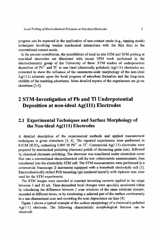
Figure 1 shows a typical example of the surface morphology of a chemically polished Ag( 1 1 1) electrode. The following characteristic morphological features can be observed:
4 E.Arnrnann, P.I. Oden, H. Siegenthaler
ic island Monoatomic pit
Fig. 1. STM image of a chemically polished Ag( 11 1) electrode in 0.0 1 M HClO4, showing stepped terrace domains with monoatomic steps, a monoatomic island, and a monoatomic pit
~41.
- The largest part of the surface consists of stepped terrace domains composed of "stacks" of monoatomic terraces. The width of the terraces in these stacked parts varies between ca. 2 nm and more than 20 nm. Exceptionally, terrace widths up to 100 nm have been observed.
- Monoatomic islands and monoatomic pits are observed regularly, with typical average widths of ca. 25 nm.
2.2 Local Progress of Pb and T1 Adsorbate Formation
2.1.1 Fast adsorption and desorption of Pb
Based on the presented typical substrate morphology shown in Fig. 1, the local progress of Pb adsorption has been systematically studied at the three morphologically different substrate domains, using a special dynamic line-scan technique described
Local Probing of Electrochemical Processes at Non-ideal Electrodes 5
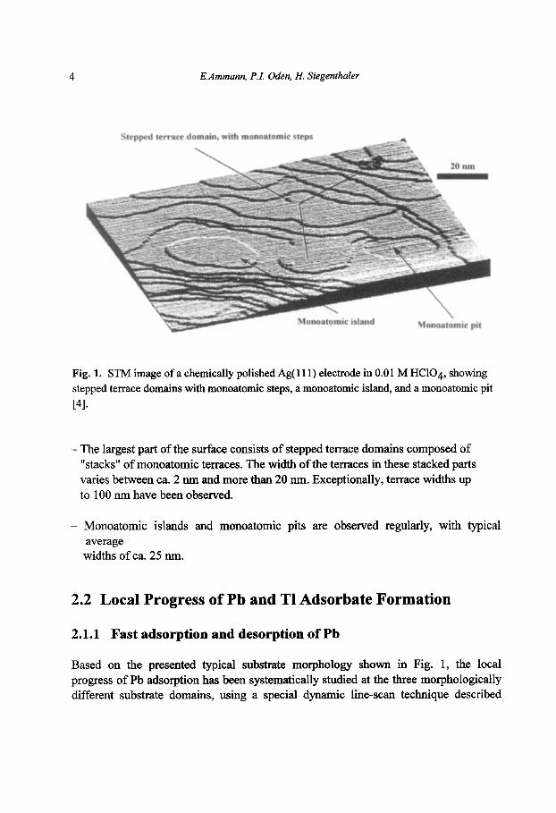
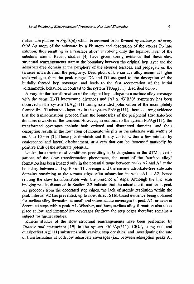
elsewhere [4] and step polarization into the various parts of the voltammetric curve investigated. The results of this STM study, presented in more detail elsewhere [4], are summarized schematically in Fig. 2 in correlation with the typical cyclic voltammogram of Pb underpotential deposition observed at macroscopic, chemically polished Ag( 1 1 1) electrodes in perchlorate-containing electrolyte [ 121.
I ' 1 ' I ' I AE[mV] 0 100 200 300
D2
steppedterraces Island -., ,
Fig.2. Schematic presentation of the local progress of Pb underpotential deposition at monoatomic pits, monoatomic islands, and stepped terrace domains of non-ideal chemically polished Ag( 11 1) electrodes [4]. For further explanation see the text.
The formation of a Pb monolayer occurs in three distinct potential ranges associated with the voltammetric adsorptioddesorption peaks Al/Dl, A2ID2, and A3D3. The local progress of adsorbate formation at the morphologically different domains of the non-ideal Ag( 1 1 1) substrate can be described as follows:
(a) The first adsorption stage, associated with the voltammetric peak A l , consists in a decoration of the steps by a spatially delimited adsorbate extending laterally ca. 1 - 3 nm from the step edge. As indicated in Fig. 2, this phenomenon is observed at all

6 E.Ammann, P.I. Oden, H. Siegenthaler
three morphological domains. Although the lateral extension of this initial coverage is remarkably stable in time scales up to several hours, it has not been possible, up to now, to resolve a stable atomic structure. It can therefore not be excluded that the adsorbate consists of a locally delimited coverage with a temporally unstable (fluctuating) structure.
(b) In the voltammetric peak A2, the growth of the adsorbate layer proceeds in the following way:
- At the stepped terrace domains, adsorption proceeds fiom the decorated step edges and leads to the formation of a "partial" adsorbate coverage, which does not completely cover the terraces, but extends only to within 1-3 nm of the peripheral terrace boundaries. The widths of these adsorbate-free peripheral domains at the external terrace boundaries conform strikingly with the widths of the step decoration coverage formed in peak A1 . This "partial" adsorbate formed after the adsorption in peak A2 has a hexagonally close-packed structure that can be imaged during a time scale of ca. lOOs, before the onset of slow structural transformations (see below).
- In the monoatomic pits, the adsorbate coverage grows inwards from the decorated pit boundaries, leading to a hexagonally close-packed (hcp) monolayer that covers the pit completely.
- On the monoatomic islands, no adsorbate layer growth has been observed up to now after step polarization into the potential range of peak A2. However, in one experiment a sequence of local formation and subsequent disappearance of a cluster-like adsorbate domain has been observed within peak A2 on an island.
(c) In the most cathodic voltammetric peak A3, the monolayer formation is completed as follows:
- At the stepped terrace domains, the adsorbate-free peripheral parts are completely covered, leading to a !'complete" hcp adsorbate that is stable over several hours.
- In the monoatomic pits, that are already covered in peak A2 by a complete adsorbate coverage, no further reaction occurs.
- On the monoatomic islanh, step polarization into the range of peak A3 leads to
Local Probing of Electrochemical Processes at Non-ideal Electrodes 7
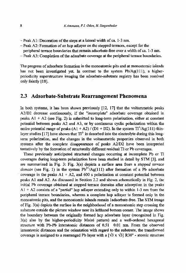
the (presumably nucleative) formation of a complete adsorbate coverage. As observed previously in an STM study by Obretenow et al. [13], the resulting
complete monolayer has a hexagonally close-packed structure with Pb-Pb interatomic distances that are compressed with regard to the values in the Pb bulk phase. In addition, a higher-periodicity Moire pattern has been observed in this system by Miiller et al. [14, 151 that has been interpreted in terms of the electronic or geometric superposition of an incommensurate Pb adlayer with the topmost substrate layer. A systematic study of the dependence of the periodicity of this Moire superstructure on the undervoltage has revealed an approximately linear decrease of the Pb-Pb nearest- neighbor distance in the hcp adlayer with decreasing undervoltage, in good agreement with the results of an in-situ GIXS study by Toney et al. [ 161.
Desorption of the complete Pb adlayer within the three distinct desorption peaks D3, D2 and D1 (see Fig. 2) by step polarization proceeds in an analogous way to the adsorption sequence, except on the monoatomic islands: in contrast to the complete adsorbate formation at the islands in peak A3, desorption in peak D3 only involves the outermost part of the monolayer at the island periphery, whereas the remaining adsorbate coverage is completely desorbed in peak D2. Desorption on the monoatomic islands occurs thus in the same way as at the stepped terrace domains, except for the missing step decoration coverage desorbed in D1.
2.2.2 Fast adsorption and desorption of T1
In earlier voltammetric experiments [17] it has been found that T1 underpotential deposition occurs in two distinctly separated potential intervals that have been associated with the successive formation of two monolayers prior to T1 bulk deposition, whereby the voltammogram in the more anodic potential range (assigned to the formation of a first monolayer) exhibits a very similar splitting into three distinct peaks AlD1, A2D2, A3/D3 as observed in the system Pb/Ag(l 1 1) (see Fig. 2).
In a recent STM study by Carnal et al. [3], these assumptions have been confiied by the observation that a hexagonally close-packed adlayer with slightly compressed TI-T1 interatomic distances is formed at more anodic potentials, followed by the formation of a second hcp adlayer with slightly disordered domains at small undervoltages. The progress of the formation of the first adsorbate layer was studied in that work by more conventional STM imaging techniques and was restricted to investigations at the stepped terrace domains. As shown in detail in [3], the formation of the fust adsorbate layer at the stepped terrace domains follows the same scheme as shown in Fig. 2 for the system Pb/Ag( 1 1 l), i.e.
8 E.Ammann, P.I. Oden, H. Siegenthaler
- Peak A1 : Decoration of the steps at a lateral width of ca. 1-3 nm. - Peak A2: Formation of an hcp adlayer on the stepped terraces, except for the
peripheral terrace boundaries that remain adsorbate-free over a width of ca. 1-3 nm. - Peak A3: Completion of the adsorbate coverage at the peripheral terrace boundaries.
The progress of adsorbate formation in the monoatomic pits and at monoatomic islands has not been investigated yet. In contrast to the system Pb/Ag(l11), a higher- periodicity superstructure imaging the adsorbate-substrate registry has been resolved only faintly [ 1 81.
2.3 Adsorbate-Substrate Rearrangement Phenomena
In both systems, it has been shown previously [12, 171 that the voltammetric peaks A2/D2 decrease continuously, if the "incomplete" adsorbate coverage obtained in peaks A1 + A2 (see Fig. 2) is submitted to long-term polarization, either at constant potential between peaks A2 and A3, or by continuous cyclic polarization within the entire potential range of peaks (A1 + A2) / (D1 + D2). In the system Tl+/Ag(lll) thin- layer studies [ 171 have shown that T1+ is desorbed into the electrolyte during this long- term polarization, and the changes in the voltammetric properties observed in both systems after the complete disappearance of peaks A2/D2 have been interpreted tentatively by the formation of structurally different residual T1 or Pb coverages.
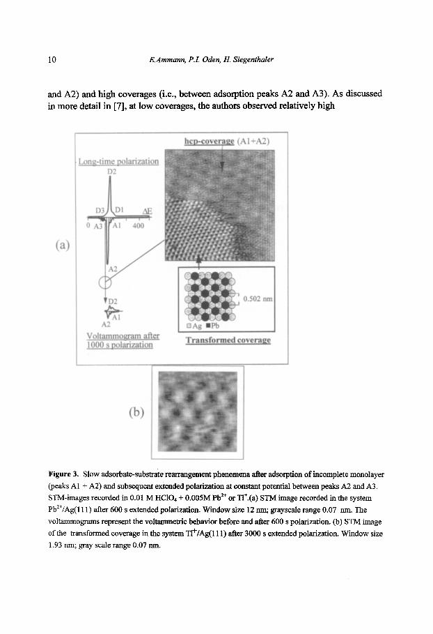
These previously anticipated structural changes occurring at incomplete Pb or T1 coverages during long-term polarization have been studied in detail by STM [3], and are summarized in Fig. 3: Fig. 3(a) depicts a surface area from a stepped terrace domain (see Fig. 1) in the system Pb2+/Ag(l 11) after formation of a Pb adsorbate coverage in the peaks A1 + A2, and 600 s polarization at constant potential between peaks A1 and A2. As discussed in Section 2.2 and shown schematically in Fig. 2, the initial Pb coverage obtained at stepped terrace domains after adsorption in the peaks A1 + A2 consists of a "partial" hcp adlayer extending only to within 1-3 nm from the peripheral terrace boundaries, whereas a complete hcp adlayer is formed only in the monoatomic pits, and the monoatomic islands remain ladsorbate-free. The STM image of Fig. 3(a) depicts the surface in the neighborhood of a monoatomic step crossing the substrate outside the picture window near its lefthand bottom corner. The image shows the boundary between the originally formed hcp adsorbate layer (recognized in Fig. 3 (a) also by the higher-periodicity Moire pattern) and a well-ordered hexagonal structure with Pb-Pb interatomic distances of 0.51 0.01 nm. From the observed interatomic distances and the orientation with regard to the substrate, the transformed coverage is assigned to a rearranged Pb layer with a [43 x 431 R30" - atomic structure
Local Probing of Electrochemical Processes at Non-ideal Electrodes 9
(schematic picture in Fig. 3(a)) which is assumed to be formed by exchange of every third Ag atom of the substrate by a Pb atom and desorption of the excess Pb into solution, thus resulting in a "surface alloy" involving only the topmost layer of the substrate atoms. Recent studies [4] have given strong evidence that these slow structural rearrangements start at the boundary between the original hcp layer and the adsorbate-free domain at the periphery of the stepped terraces, and propagate on the terraces inwards from the periphery. Desorption of the surface alloy occurs at higher undervoltages than the peak ranges D2 and D1 assigned to the desorption of the initially formed hcp coverage, and leads to the fast recuperation of the initial voltammetric behavior, in contrast to the system TVAg(l1 l), described below.
A very similar transformation of the original hcp adlayer to a surface alloy coverage with the same T1-T1 interatomic distances and [d3 x d3]R3Oo symmetry has been observed in the system TVAg(ll1) during extended polarization of the incompletely formed first T1 adsorbate layer. As in the system Pb/Ag(l 1 l), there is strong evidence that the transformations proceed from the boundaries of the peripheral adsorbate-free domains inwards on the terraces. However, in contrast to the system Pb/Ag(l 1 l), the transformed coverages include both ordered and disordered domains, and their desorption results in the formation of monoatomic pits in the substrate with widths of ca. 3 to 10 nm [3]. These pits diminish and finally vanish within a few minutes by coalescence and lateral displacement, at a rate that can be increased markedly by positive shift of the substrate potential.
Under the experimental conditions prevailing in both systems in the STM investi- gations of the slow transformation phenomena, the onset of the 'lsurface alloy" formation has been imaged only in the potential range between peaks A2 and A3 at the boundary between an hcp Pb or T1 coverage and the narrow adsorbate-free substrate domains remaining at the terrace edges after adsorption in peaks A1 + A2, hence relating the slow transformation with the presence of steps. Although the line scan imaging results discussed in Section 2.2 indicate that the adsorbate formation in peak A2 proceeds from the decorated step edges, the lack of atomic resolution within the peak interval A2 has prevented, up to now, direct STM-based evidence being obtained for surface alloy formation at small and intermediate coverages in peak A2, or even at decorated steps within peak A1 . Whether, and how, surface alloy formation also takes place at low and intermediate coverages far from the step edges therefore remains a subject for M e r studies.
Kinetic studies of the slow structural rearrangements have been performed by Vitunov and co-workers [19] in the system Pb2'/Ag(111), C104-, using real and quasiperfect Ag( 1 1 1) substrates with varying step densities, and investigating the rate of transformation at both low adsorbate coverages (i.e., between adsorption peaks A1
10 E.Ammann, P.I. Oden, H. Siegenthaler
and A2) and high coverages (i.e., between adsorption peaks A2 and A3). As discussed in more detail in [7], at low coverages, the authors observed relatively high
hce-coverage (Al+A2)
Transformed coverape
A2 Vol tammom after 1000 s uolarization
Figure 3. Slow adsorbate-substrate rearrangement phenomena after adsorption of incomplete monolayer
beaks A1 + A2) and subsequent extended polarization at constant potential between peaks A2 and A3. STM-images recorded in 0.01 M HC104 + 0.005M Pb2+ or Tl'.(a) STM image recorded in the system
Pb2+/Ag( 1 1 1) after 600 s extended polarization. Window size 12 nm; grayscale range 0.07 nm. The voltammograms represent the voltammetric behavior before and after 600 s polarization. @) STM image of the transformed coverage in the system ll+/Ag(lll) after 3000 s extended polarization. Window size 1.93 nm; gray scale range 0.07 nm.
Local Probing of Electrochemical Processes at Non-ideal Electrodes 11
transformation rates that were independent of the step densities, whereas a strong dependence of the rates of the step densities was found at high coverages, corresponding to the conditions of the STM studies described above. The measurements were related to kinetic site exchange models including surface inhomogeneities at low adsorbate coverages, and choosing a one-dimensional diffusion model without consideration of surface inhomogeneities for high coverages. However, there remain uncertainties about the dependencies of the transformation rates on the surface inhomogeneities that require further elucidation [7].
3 Conclusions and Outlook
The presented results demonstrate the relevance of the nanometer-scale morphology (stepped terrace domains, monoatomic islands and monoatomic pits) for the local progress of adsorbate formation and adsorbate stability. The stepwise formation of the Pb and T1 adsorbate coverages, combined with the slow formation of a surface alloy coverage, illustrates experimentally thermodynamic and kinetic aspects of various growth modes of metal deposits discussed recently [7, 201. In the two systems presented, the complete hcp monolayer coverages formed during fast adsorption of Pb and T1 represent obviously metastable systems, whereas the surface alloy coverage formed during extended polari-zation of incomplete adsorbate layers is considered to be the thermodynamically stable coverage. The experiments described indicate that in- situ STM is specially suitable for local measurements. Further insight into the role of atomic-scale inhomogeneities in the local progress of electrochemical processes can be expected, e.g., from the use of nanostructured model electrodes.
Acknowledgements. The authors acknowledge gratefully the financial support by the Schweiz. Nationalfonds, and they thank F. Niederhauser for technical support.
References
A.A. Gewirth, H. Siegenthaler (Eds.), Nanoscale Probes of the Solidniquid Interface, NATO Series E, Applied Sciences, Vol. 288, Kluwer Academic Publishers, Dordrecht, 1995. Scanning Tunneling Microscopy II, R. Wiesendanger, H.-J. Giintherodt (Eds.), Springer Series on Surface Sciences, Vol. 28, Springer-Verlag, Berlin, 1995.
12 E.Ammann, P.I. Oden, H. Siegenthaler
[3] D. Carnal, P.I. Oden, U. Miiller, E. Schmidt, H. Siegenthaler, Electrochim. Acta 40, 1223 (1995).
[4] E. Ammann, Diploma Thesis, University of Bern, 1995; E. Ammann H. Siegenthaler, submitted to J. Electrochem. SOC.
[5] U. Schmidt, S. Vinzelberg, G. Staikov, Surf. Sci. 348,261 (1996). [6] J.X. Wang, R.R. Adzic, O.M. Magnussen, B.M. Ocko, Surf. Sci. 344, 11 (1995). [7] E. Budevski, G. Staikov, W.J. Lorenz, Electrochemical Phase Formation and Growth -
An Introduction to the Initial Stages of Metal Deposition. VCH, Weinheim, 1996. [8] Y.T. Kim, H. Yang,A.J. Bard, J. Electrochem. SOC. 138, L71 (1991). [9] R. Nyffenegger, C. Gerber, H. Siegenthaler, Synth. Metals 55-57,402 (1993). [lo] H.Yang, F.-R.Fan, Sh.-L.Yau, A.J.Bard, J. Electrochem. SOC. 139,2182 (1992). [ 113 R. Nyffenegger, E. Ammann, H. Siegenthaler, R. Kotz, 0. Haas, Electrochim. Acta 40,
[12] H. Siegenthaler, K. Juttner, Electrochim. Acta 24, 109 (1979). [13] W. Obretenow, M. Hopfher, W.J. Lorenz, E. Budevski, G. Staikov, H. Siegenthaler, Surf.
[14] U. Miiller, D. Carnal, H. Siegenthaler, E. Schmidt, W.J. Lorenz, W. Obretenow, U.
[ 151 U. Miiller, D. Carnal, H. Siegenthaler, E. Schmidt, W.J. Lorenz, W. Obretenow, U.
[16] M.F. Toney, J.G. Gordon, G.L. Borges, O.W. Melroy, D. Yee, L.B. Sorensen, Phys.
[17] H. Siegenthaler, K.. Juther, E. Schmidt, W.J. Lorenz, Electrochim. Acta 23, 1009 (1978) [18] P.I. Oden, unpublished results. [ 191 A. Popov, N. Dimitrov, D. Kashchiev, T. Vitanov, E. Budevski, Electrochim. Acta 38,
[20] W.J. Lorenz, G. Staikov, submitted.
1411 (1995).
Sci. 271,191 (1992).
U.Schmidt, G. Staikov, E.Budevski, Phys. Rev. B 46,12899 (1992).
Schmidt, G. Staikov, E. Budevski, Phys. Rev. B 49,7795 (1994).
Rev.B 45,9362 (1992).
2 173 (1992), and references by the same authors cited therein.
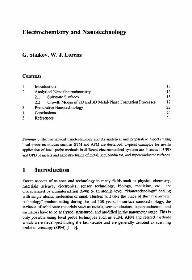
Electrochemistry and Nanotechnology
G. Staikov, W. J. Lorenz
Contents
1 Introduction 13 2 Analytical Nanoelectrochemistry 15
2.1 Substrate Surfaces 15 2.2 Growth Modes of 2D and 3D Metal-Phase Formation Processes 17
4 Conclusions 24 5 References 24
3 Preparative Nanotechnology 22
Summary. Electrochemical nanotechnology and its analytical and preparative aspects using local probe techniques such as STM and AFM are described. Typical examples for in-situ application of local probe methods in different electrochemical systems are discussed: UPD and OPD of metals and nanostructuring of metal, semiconductor, and superconductor surfaces.
1 Introduction
Future aspects of science and technology in many fields such as physics, chemistry, materials science, electronics, sensor technology, biology, medicine, etc., are characterized by miniaturization down to an atomic level. “Nanotechnology” dealing with single atoms, molecules or small clusters will take the place of the “micrometer technology” predominating during the last 150 years. In surface nanotechnology, the surfaces of solid-state materials such as metals, semiconductors, superconductors, and insulators have to be analyzed, structured, and modified in the nanometer range. This is only possible using local probe techniques such as STM, AFM and related methods which were developed during the last decade and are generally denoted as scanning probe microscopy (SPM) [l - 91.
14 G. Staikov, KJ. Lorenz
Analytical and preparative aspects of modern nanotechnology can be distinguished. Local probe investigations of surface thermodynamics, structure, dynamics, and reactions belong to the analytical aspect. On the other hand, surface nanostructuring or surface modification and the preparation of defined “nanoobjects” by local probe techniques represent the preparative aspect.
Local probe techniques are carried out “ex-situ”, “non-sib” or “ in -~ i tu~~ with respect to applied environmental conditions. Ex-situ local probe investigations are performed under UHV conditions on well-defined substrates, e.g., single-crystal surfaces. Such ex-situ measurements are often made in far from real conditions, which are characterized by adsorption and film formation. Therefore, ex-situ UHV techniques are usually combined with appropriate transfer devices to switch substrates from the real environment to UHV and vice versa. Non-situ local probe measurements are also started under UHV conditions to characterize the bare substrate surface, but they are continued under a finite vapor pressure in order to form adsorbates or mono- or multi- atomic (-molecular) films modeling real environmental conditions. In-situ local probe measurements are carried out at solidliquid or solidgas interfaces under defined real conditions involving adsorption and film formation.
In-situ local probe investigations at solidliquid interfaces can be performed by electro-chemical means if both phases are electronically and ionically conducting. In this case, electrochemistry offers a great advantage since the Fermi levels [lo], EF, of both substrate and tip (or metallized cantilever) can be adjusted precisely and independently of each other using bipotentiostatic control in a four-probe technique (substrate as working electrode; tip or conducting cantilever as local probe ,,sonde“; reference and counter electrodes) [S]. In STM studies, this Fenni level control leads to defined surface properties at tip and substrate and, therefore, to defrned tunneling conditions for distance tunneling spectroscopy (DTS) and voltage tunneling spectroscopy (VTS). Without bipotentiostatic conditions, only the potential difference between tip and substrate, i.e., the tunneling voltage Et = Etip - E, can be held constant without control of the surface properties and, therefore, of the tunneling conditions.
A further advantage of electrochemical in-situ SPM studies of two- and three- dimensional phase formation processes is the possibility of controlling accurately the supersaturation or undersaturation, Ap, which can be correlated, in the absence of other kinetic hindrances with overpotential and underpotential, respectively [ 1 13 :