electrical system for autonomous underwater vehicle and
TRANSCRIPT

Electrical System for Autonomous
Underwater Vehicle and Autonomous
Surface Vehicle
Submitted by
Vanessa Cassandra
Department of Electrical and Computer Engineering
In partial fulfillment of the requirements for the
Degree of Bachelor of Engineering
National University of Singapore

1
Abstract
Team Bumblebee has been developing Bumblebee Autonomous Underwater
Vehicle (AUV) version 3.0 since August 2014 and it finally made its debut during
Singapore Autonomous Underwater Vehicle Challenge in March 2016. From the
initial stage of conception until the deployment of the vehicle, there are
problems that were not foreseen and only arose during operation.
Improvements need to be made to make the system more robust and reliable.
Team Bumblebee has also started the development of an Autonomous Surface
Vehicle (ASV) and it will be deployed during Maritime RobotX Challenge in
December 2016.
This paper discusses the improvements that can be made for Bumblebee AUV
version 3.0 to ensure a stable system and also about the electrical architecture of
the ASV.

2
Acknowledgement
First and foremost, I would like to express my gratitude to God, who gave me an
opportunity to work on a project that I care about, and my strength in times of
weary.
I would also like to express my gratitude to my supervising professor, Professor
Mandar Anil Chitre, who gave me the opportunity to work under his supervision.
I really appreciate the freedom given for me on how to carry out my project and
his guidance throughout the project.
I would also like to thank the members of Team Bumblebee for giving me the
platform for the project. They give me moral support as comrades with the same
cause.
There are many people who contributed to my life and this project that I am not
able to mention one by one, but their contribution will not be forgotten.

3
Table of Contents Abstract .................................................................................................................................. 1 Acknowledgement .............................................................................................................. 2 Table of Contents ................................................................................................................ 3 List of Figures ....................................................................................................................... 4 List of Tables ........................................................................................................................ 5 List of Symbols and Abbreviations ............................................................................... 6 1 Introduction .................................................................................................................. 7
1.1. Background of the project ............................................................................................ 7 1.2. Aim of the project ............................................................................................................ 9 1.3. Scope of the project ......................................................................................................... 9
2 Autonomous Underwater Vehicle (AUV) .......................................................... 10 3 AUV Backplane ........................................................................................................... 12 4 AUV Existing Problems and Solutions ............................................................... 15
4.1. Problem 1: Unreliable power supply at 5V level ...............................................15 4.2. Solution 1: Different DC-DC converter topology .................................................17 4.3. Problem 2: Incorrect voltage level in soft-start output .......................................20 4.4. Solution 2: Zener diode as clamping diode ..........................................................21 4.5. Problem 3: Unreliable USB to UART connection ....................................................24 4.6. Solution 3: Proper circuit design and Electrostatic Discharge (ESD) protection .....................................................................................................................................25
4.6.1. Differential Signaling PCB layout ...................................................................................... 26 4.6.2. Electrostatic Discharge (ESD) Protection ................................................................ 28 4.6.3. Ground ......................................................................................................................................... 30
4.7. Result .....................................................................................................................................32 5 ASV Electronics Components ................................................................................ 33
5.1. Thrusters ..........................................................................................................................33 5.2. Battery ...................................................................................................................................35
5.2.1. Deep-cycle lead-acid boat batteries ............................................................................ 35 5.2.2. Lithium-ion batteries ........................................................................................................ 37 5.2.3. Comparison between lead-acid and lithium-ion batteries ................................ 38 5.2.4. ASV Battery ................................................................................................................................ 40
5.3. Proximity sensors .............................................................................................................42 6 ASV Electronics Board ............................................................................................ 43
6.1. Soft start ................................................................................................................................43 6.2. Load sharing capability ...................................................................................................44 6.3. UART to RS485 converter ...............................................................................................44 6.4. Power over Ethernet (POE) injector ...........................................................................45 6.5. Breakout connector ..........................................................................................................47
7 ASV Electronics Boards ........................................................................................... 48 8 ASV Electrical Architecture .................................................................................. 50 9 Conclusion ................................................................................................................... 51 References .......................................................................................................................... 52

4
List of Figures
Figure 1. Bumblebee AUV 1.0 ...................................................................................................... 7 Figure 2. Bumblebee AUV 2.0 ...................................................................................................... 8 Figure 3. Bumblebee AUV 3.0 ...................................................................................................... 8 Figure 4. WAM-V platform for an ASV (www.wam-v.com) ............................................. 9 Figure 5. Bumblebee AUV 3.0 Hardware Architecture................................................... 10 Figure 6. Bumblebee AUV 3.0 Power Architecture .......................................................... 11 Figure 7. Electrical backplane with three daughter boards slotted in it ................. 12 Figure 8. Bumblebee AUV 3.0 electrical rack ..................................................................... 12 Figure 9. Power and data links between backplane and other major electronics13 Figure 10. Electrical architecture of the backplane ......................................................... 14 Figure 11. M4-ATX from Mini-box ......................................................................................... 15 Figure 12. Changes in the 5V line when thrusters are running .................................. 16 Figure 13. AC coupling to remove DC components ......................................................... 16 Figure 14. Topology of Murata isolated DC-DC converter ............................................ 19 Figure 15. N-channel MOSFET based soft-start circuitry .............................................. 20 Figure 16. Zener diode I-V characteristic (www.eeweb.com).................................... 22 Figure 17. Application circuit for zener diode as a clamping diode
(www.eeweb.com) .............................................................................................................. 23 Figure 18. The USB to UART converter circuitry .............................................................. 25 Figure 19. PCB design guide for differential pair (Intel, 2000) ................................... 27 Figure 20. USB differential pair routing in the backplane ............................................ 28 Figure 21. Design guidelines for bypass capacitor (FTDI, 2013) ............................... 29 Figure 22. Recommended use of TVS on USB to UART converter circuitry (FTDI,
2013) ........................................................................................................................................ 30 Figure 23. USB ground plane on the backplane ................................................................ 31 Figure 24. AUV backplane before modification ................................................................ 32 Figure 25. AUV backplane before specification................................................................. 32 Figure 26. Wave Adaptive Modular Vessel platform (www.wam-v.com) .............. 33 Figure 27. Torqeedo Cruise 2.0R (left) and MinnKota RT80 (right)......................... 34 Figure 28. Lead-acid batteries charge state (Albright, Edie & Al-Hallaj, 2012) .... 35 Figure 29. Lithium-ion batteries charge (Albright, Edie & Al-Hallaj, 2012) .......... 37 Figure 30. Batteries cycle life in moderate climate (average 25qC) (Albright, Edie
& Al-Hallaj, 2012) ................................................................................................................ 39 Figure 31. Batteries cycle life in hot climate (average 33qC) (Albright, Edie & Al-
Hallaj, 2012) .......................................................................................................................... 39 Figure 32. Voltage comparison of batteries (Albright, Edie & Al-Hallaj, 2012) .... 40 Figure 33. Torqeedo Power 26-104 battery ....................................................................... 41 Figure 34. MaxBotix MB7383 proximity sensor ............................................................... 42 Figure 35. N-channel MOSFET based soft-start circuit .................................................. 43 Figure 36. Load-sharing circuit using LTC4416 ................................................................ 44 Figure 37. Typical half-duplex RS485 network (Maxim Integration) ...................... 45 Figure 38. Pin allocation for POE on RJ45 cable (www.wisptech.com) ................... 46 Figure 39. Stacked RJ45 connector for POE injector (www.global-sources .com)
.................................................................................................................................................... 46 Figure 40. PCB implementation of POE injector ............................................................... 47

5
Figure 41. Power and data links between the electronics board and the other ASV components ........................................................................................................................... 48
Figure 42. ASV electronics board architecture .................................................................. 49 Figure 43. ASV data connectivity architecture .................................................................. 50 Figure 44. ASV power architecture ........................................................................................ 50
List of Tables Table 1. Power rating for the electrical components of the vehicle .......................... 18 Table 2. WAM-V specifications (Anderson, 2014) ........................................................... 34 Table 3. Thrusters specifications ............................................................................................ 34 Table 4. Comparison between batteries chemistry (Albright, Edie & Al-Hallaj,
2012) ........................................................................................................................................ 38 Table 5. Torqeedo Power 26-104 specifications .............................................................. 41 Table 6. MaxBotix MB7383 specifications .......................................................................... 42

6
List of Symbols and Abbreviations AGM Absorbed Glass Mat AHRS Attitude Reference Heading System ASV Autonomous Surface Vehicle AUV Autonomous Underwater Vehicle CAN Controller Area Network DC Direct Current DoD Depth of Discharge GEDC Gyro Enhanced Attitude & Heading System GigE Gigabit Ethernet IMU Inertial Measurement Unit Li-po Lithium-polymer LED Light Emitting Diode MCU Microcontroller Unit MOSFT Metal-oxide Field Effect Transistor N-MOSFET N-channel Metal-oxide Field Effect Transistor P-MOSFET P-channel Metal-oxide Field Effect Transistor PCB Printed Circuit Board POE Power over Ethernet PWM Pulse Width Modulation RJ45 Registered Jack 45 SBC Single Board Computer TTL Transistor-Transistor Logic UART Universal Asynchronous Receiver/Transmitter USB Universal Serial Bus A Ampere Ah Ampere hour kg kilogram kgf kilogram-force lbs pound m meter s second V Volt W Watts : Ohm

7
1 Introduction
1.1. Background of the project
Bumblebee Autonomous Underwater Vehicle (BBAUV) is a student-led group
formed in Summer 2012 by five students in the Mechanical Engineering
department. The team develops an Autonomous Underwater Vehicle (AUV) to
compete in two international competitions every year: Singapore Autonomous
Underwater Vehicle Challenge (SAUVC) and RoboSub competition in San Diego,
USA.
Over the years, the team has developed three vehicles, which are Bumblebee 1.0,
Bumblebee 2.0, and the latest, Bumblebee 3.0.
Figure 1. Bumblebee AUV 1.0

8
Figure 2. Bumblebee AUV 2.0
Figure 3. Bumblebee AUV 3.0
As part of the team vision, “To engineer the autonomous system of the future”,
Team Bumblebee decided to venture to other unmanned system domain, the
Autonomous Surface Vessel (ASV). The team is going to develop an ASV on a
Wave Adaptive Modular Vessel (WAM-V) platform and participate in Maritime
RobotX Challenge that is held once in two years.

9
Figure 4. WAM-V platform for an ASV (www.wam-v.com)
The next Maritime RobotX Challenge will be held in Hawaii in December 2016.
The teams participating are required to produce the propulsion, control, and
sensor systems necessary to complete the competition tasks. The competition
consists of tasks such as demonstrating navigation and control, acoustic signal
localisation, identification of symbols and colours, and obstacles detection and
avoidance.
1.2. Aim of the project
This project’s objective is to improve the electrical system of the Bumblebee 3.0,
especially on the electrical backplane, and also to choose appropriate electronics
components for the ASV and to design a custom electronics board to interface
the components with the main processing unit, the Single Board Computer (SBC).
1.3. Scope of the project
1. To identify the existing electrical problems in Bumblebee AUV 3.0
2. To explore and provide solutions to the problems

10
3. To choose appropriate electronics components, namely the thrusters,
batteries, and sensors of the ASV
4. To design an electronics board to interface these components with the
main computer.
2 Autonomous Underwater Vehicle (AUV)
The current electrical system of Bumblebee AUV 3.0 is as described in the block
diagrams below:
Figure 5. Bumblebee AUV 3.0 Hardware Architecture
11
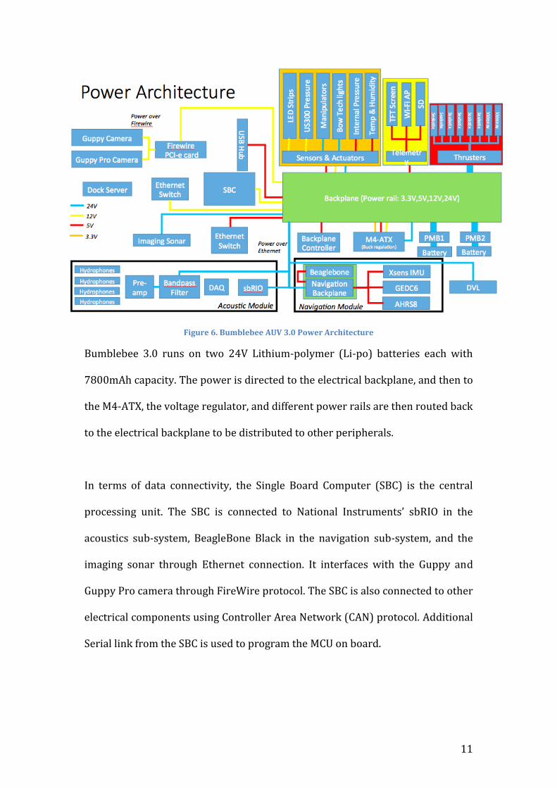
Figure 6. Bumblebee AUV 3.0 Power Architecture
Bumblebee 3.0 runs on two 24V Lithium-polymer (Li-po) batteries each with
7800mAh capacity. The power is directed to the electrical backplane, and then to
the M4-ATX, the voltage regulator, and different power rails are then routed back
to the electrical backplane to be distributed to other peripherals.
In terms of data connectivity, the Single Board Computer (SBC) is the central
processing unit. The SBC is connected to National Instruments’ sbRIO in the
acoustics sub-system, BeagleBone Black in the navigation sub-system, and the
imaging sonar through Ethernet connection. It interfaces with the Guppy and
Guppy Pro camera through FireWire protocol. The SBC is also connected to other
electrical components using Controller Area Network (CAN) protocol. Additional
Serial link from the SBC is used to program the MCU on board.

12
3 AUV Backplane
Figure 7. Electrical backplane with three daughter boards slotted in it
Figure 8. Bumblebee AUV 3.0 electrical rack
AUV backplane is a custom printed circuit board (PCB) with the main functions
of:
- Providing power to the peripherals
- Providing data connectivity to peripherals
- Current and voltage monitoring
- Power control

13
Figure 9. Power and data links between backplane and other major electronics
Figure 9 shows that the backplane is responsible to distribute power to other
peripherals. After taking in power from two external batteries, it powers the
voltage regulator, M4-ATX with load-balanced 24V output, and the M4-ATX gives
back 12V, 5V, and 3.3V back to the backplane. The backplane then routes the
different voltages to power respective electronics inside and outside the main
hull.
Other than for power distribution unit, the backplane also provides data
connectivity from the SBC to other peripherals. There are 6x USB to UART
converter circuitries to provide connectivity from the SBC to the Microcontroller

14
Unit (MCU) of the backplane and the daughter boards. It also has UART to CAN
converter, thus allowing the SBC to join in the CAN bus.
Figure 10. Electrical architecture of the backplane
The power circuitries of the backplane include the soft-start function, load-
balancing, and voltage and current measurement.
As the processing unit, the backplane MCU will receive the voltage and current
reading and it will control the power input to the three daughter boards:
thruster board, sensor & actuator board, and telemetry board. It will also control
the power input to the Power over Ethernet (POE) devices through its POE
injector feature.

15
The CAN circuitries consist of CAN controller and transceiver, enabling the
backplane to communicate through the CAN bus. It also has a UART to CAN
converter. The SBC that communicates with the backplane through UART can
now join the CAN bus to talk to other CAN peripherals.
The design of the backplane has been done last year and each feature has been
tested individually. However, the bigger challenge is in the integration of the
backplane with the rest of the components and making sure that it is reliable
during operation.
4 AUV Existing Problems and Solutions
4.1. Problem 1: Unreliable power supply at 5V level
To convert 24V to 12V, 5V, and 3.3V power rails, the voltage regulator used in
the AUV is M4-ATX, which is a Power Supply Unit (PSU) from Mini-box. M4-ATX
is using buck/boost converter topologies to convert the DC line.
Figure 11. M4-ATX from Mini-box
16
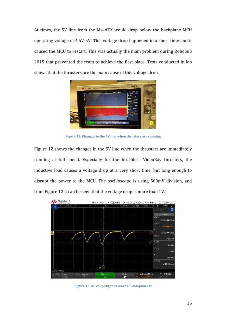
At times, the 5V line from the M4-ATX would drop below the backplane MCU
operating voltage of 4.5V-5V. This voltage drop happened in a short time and it
caused the MCU to restart. This was actually the main problem during RoboSub
2015 that prevented the team to achieve the first place. Tests conducted in lab
shows that the thrusters are the main cause of this voltage drop.
Figure 12. Changes in the 5V line when thrusters are running
Figure 12 shows the changes in the 5V line when the thrusters are immediately
running at full speed. Especially for the brushless VideoRay thrusters, the
inductive load causes a voltage drop at a very short time, but long enough to
disrupt the power to the MCU. The oscilloscope is using 500mV division, and
from Figure 12 it can be seen that the voltage drop is more than 1V.
Figure 13. AC coupling to remove DC components

17
From there, AC coupling capabilities of the oscilloscope is used to eliminate the
DC component. A threshold is set such that the oscilloscope will capture the
moment of when the voltage is lower than the threshold. From the figure, it can
be seen that the power line on the 5V rail experiences a voltage drop of more
than -1.3V in the span of 200 microseconds, and this is when the MCU restarted.
Sometimes, the voltage drop can be even as low as -1.7V. The testing was done
several times to ascertain that the voltage drop caused by the inductive load of
the thruster is the main cause of the problem. Out of 10 times the testing is
conducted, the embedded system restarted 4 times.
4.2. Solution 1: Different DC-DC converter topology
To understand how to mitigate this problem, a further study on the different DC-
DC converter topologies is needed.
DC-DC converter topologies generally divided into two categories: transformer-
isolated and non-transformer. In each category, there are several topologies,
with some available in both forms. The non-isolated converters are inexpensive
solution to many applications and are often used for small voltage conversions.
However, unlike the isolated converters, they are not protected against high
input voltages or transients (Wurth Electronics, 2012). The isolated converter
has more complex circuits and it requires a higher number of components, hence
it’s more costly.

18
According to the datasheet, the M4-ATX uses switching regulator with buck and
boost converter topologies. To prevent the transient voltage caused by the
thrusters, an isolated converter topology is explored instead. Isolated DC-DC
converter provides physical separation between the input and the output
through the use of galvanic isolation between the two.
To choose the proper DC-DC converter, it is important to consider the power
rating of the whole electronic system of the vehicle.
Components Voltage Rating (V)
Current Rating (A) Power (W)
Outside the main hull Bandpass filter / pre-amplifier 24 0.5 12 NI sbRIO 24 0.5 12 Imaging sonar 24 0.5 12 GEDC 5 0.5 2.5 AHRS-8 5 0.5 2.5 XSENS IMU 5 0.5 2.5 BeagleBone Black 5 0.5 2.5 Total 46 Inside the main hull SBC 12 4.25 51 LED Strip 12 1 12 Ethernet switch 12 1 12 Camera & card 12 0.5 6 5x ATMega2560 5 2.5 12.5 Assorted Ics 5 0.5 2.5 Telemetry 3.3 1 3.3 Total 99.3
Table 1. Power rating for the electrical components of the vehicle
19
If an isolated DC-DC converter is going to be used, two isolated DC-DC converters
are needed: one for the electronics inside the main hull, and another one for
those outside the hull, which are the acoustics sub-system and the navigation
sub-system. From Table 1, the isolated DC-DC converter that is to be chosen has
to withstand more than 99.3W of power. It is quite challenging to find a 24V
isolated DC-DC converter with such rating, and the closest one that is found is a
24V – 24V isolated DC-DC converter by Murata model UVQ-24/4.5-D24PB-C with
power rating of 108W. However, for the main hull, since the power rating is too
close with the minimum rating calculated in Table 1, this model might not be
appropriate. Instead, a 24V – 12V isolated DC-DC converter by Murata model
UWQ-12/17-Q48PB-C can be used for testing, since it has higher power rating of
204W.
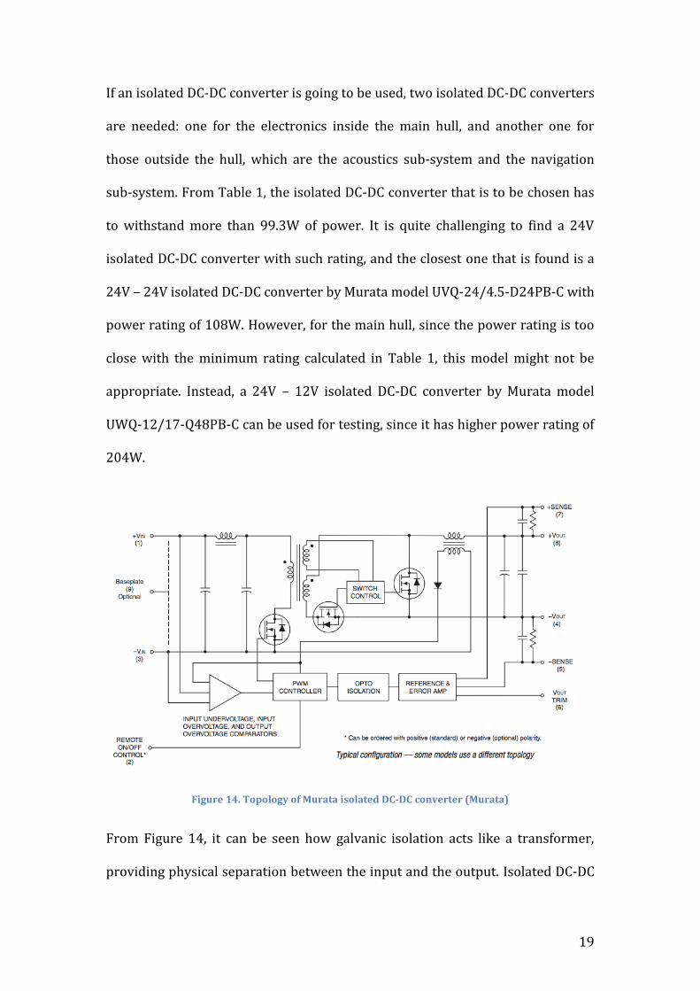
Figure 14. Topology of Murata isolated DC-DC converter (Murata)
From Figure 14, it can be seen how galvanic isolation acts like a transformer,
providing physical separation between the input and the output. Isolated DC-DC

20
converters have strong noise and interference blocking capability thus provide
the load with a cleaner DC source (Texas Instruments, 2015).
For testing, a 24V – 12V isolated DC-DC converter by Murata model UWQ-12/17-
Q48PB-C was tested with the same setup that caused the embedded system of
the AUV to die. The DC-DC converter is placed between the battery and the
voltage regulator, M4-ATX. After 20 times of running the thrusters in full speed,
with the same oscilloscope setup (AC coupling with trigger detection), there was
no voltage drop at all. This shows that implementing the isolated DC-DC
converter make the system stable and address the power issue.
4.3. Problem 2: Incorrect voltage level in soft-start output
The backplane has a soft-start capability to prevent in-rush current to the
system.
Figure 15. N-channel MOSFET based soft-start circuitry
The circuitry uses N-channel MOSFET that will be turned on slowly by gradually
supplying voltage to the VGS gate-to-source voltage. This is achieved by charging
the capacitor connected between the gate and the source of the MOSFET.
Resistor R1 and C1 act like an RC filter, and the time taken to reach 63% of the

21
steady-state voltage is given by W = R x C. The time constant was decided to be 1s,
because it was known experimentally that to control the in-rush current
effectively, the time constant has to be higher than 10ms. Thus the R1 and C1
were determined to be 1M: and 1PF respectively. The value of R2 was chosen to
be 1M: as well, since the voltage divider network of R1 and R2 should generate
voltage that is higher than the clamping voltage of the Zener Diode, which is 10V.
By making R1 and R2 to be the same, the voltage at the voltage divider network
will be 12V, half the voltage of the supply voltage.
The output of the soft-start circuitry will be routed to the load-balancing feature
on the backplane, that will balance the load drawn from the two batteries.
However, the main problem is that, although the steady-state voltage output of
the soft-start circuitry should be 24V, in reality it often happens that the output
voltage is only around 17V or sometimes even less than that.
4.4. Solution 2: Zener diode as clamping diode
To solve this problem, it is important to understand how zener diode works as a
clamping diode to limit the voltage in the circuitry. In the soft-start circuitry, a
zener diode is used to clamp the 12V from the voltage divider network down to
10V.
A normal diode usually blocks current that is flowing in reverse direction, and
eventually it will suffer damage when the reverse voltage is too high. However,

22
Zener Diode, which is sometimes called “Breakdown Diode”, is purposely
designed to break down and clamp the voltage level in the process.
When zener diode is biased in the forward direction, it behaves just like a normal
diode passing the rated current, but when reverse voltage that is higher than the
rated voltage applied across the diode, Avalanche Breakdown will occur and
current will start to flow through to limit this increase in voltage.
Figure 16. Zener diode I-V characteristic (www.eeweb.com)
The voltage point when the zener diode starts breaking down is denoted as the
“zener breakdown voltage”, Vz.

23
Figure 17. Application circuit for zener diode as a clamping diode (www.eeweb.com)
Figure 17 shows a typical application on how a zener diode is used to clamp the
output voltage. The resistor connected in series with the diode limits the current
flowing through the circuit. The output voltage is taken across the zener diode.
The cathode terminal of the diode is connected to the positive rail, so that it will
be operating at its breakdown condition.
The soft-start circuitry in the backplane satisfies the above application circuit of
the zener diode. However, the design misses out a small component of the
circuit. In the I-V characteristics of the zener diode in Figure 16, it’s important to
take note that there is a minimum current required for the diode to operate,
denoted by IZ(min).
In the soft-start circuitry in Figure 15, the value of R1, R2, and C1 are 1M:, 1M:,
and 1PF respectively. The total effective resistance of R1 and R2 will be 2M:,
and with supply voltage of 24V, at steady-state voltage, the current flowing to the
circuit will be:

24
I = V/R = 24V/2M: = 12PA
The zener diode used in the backplane is MMSZ4697 from Fairchild
Semiconductor. From the data sheet, the test condition at which the zener
voltage will clamp to 10V is when the reverse current IZ is at 50PA.
There is not enough current flowing through the zener diode and hence it was
not functioning properly. Thus, a new value set needs to be decided such that
more than 50PA of current is flowing through the diode and the time constant of
the RC filter in the circuit is more than 10ms. A new set of value for R1, R2, and
C1 is to be: 10k:, 10k:, and 10PF.
W = R x C = 10k: x 10PF= 0.1
I = V/R = 24V/20k: = 1.2mA
The time constant is reduced to 0.1s, but it is still significantly higher than the
required 10ms. After changing the value of the resistors and capacitors, the
output of the soft-start circuitry is giving the correct voltage level of 24V.
4.5. Problem 3: Unreliable USB to UART connection
The backplane features a USB to UART converter that provides communication
between the SBC and the MCU in the backplane and the daughter boards.
Although the prototype of the circuit works, it is observed that there are a lot of
problems with the connection during operation.

25
Figure 18. The USB to UART converter circuitry
The USB to UART converter circuitry consists of three main components: the
current limiter load switch, the USB to UART converter IC FT232RL, and the
opto-isolator IC ADUM1402. The circuitry design was unreliable that many
times, the simple act of plugging in the USB cable to the USB connector may kill
the USB to UART converter IC, the load switch, or the opto-isolator IC.
4.6. Solution 3: Proper circuit design and Electrostatic Discharge
(ESD) protection
At closer inspection, there are many improvements that can be done on the
circuit. Some of them are, for example, designing PCB that is suitable for
differential signaling and ESD protection, putting an on-board ESD protection,
and taking care of the grounding of the USB connectors.

26
4.6.1. Differential Signaling PCB layout
With the use of FT232R for the USB to UART IC, there are some guidelines that
were not implemented in the current backplane design.
In USB connection, data transfers require two signals that are complementary of
each other. This is called a differential pair. Differential signaling is also used in
other technologies such as Ethernet and RS-485. Especially for USB, there are
specific requirements mentioned in the USB 2.0 specifications (Intel, 2000)
regarding shielding, signal, and power conductor.
USB connector at the PCB consists of 4 main signals: VBUS (5V power), Ground,
Data Plus (DP), and Data Minus (DM). DP and DM are the differential pair.
According to USB 2.0 design guidelines, these two signals must be closely
matched with the following characteristics:
1. Equal length: Both the DP and the DM signals must have equal trace
length. If one is longer than the other, it will affect the timing of the
signals and may result in data errors.
2. Impedance: the impedance of the twisted pair cabling in the USB cable
must match the impedance in the PCB in order to minimize signal
reflections. USB signals are 90Ω differential to each other / 45Ω each to
Signal Ground.
3. No stubs: when adding other components, such as Transient Voltage
Suppressors, the DP and DM signals should not have any T’s to minimize
signal reflections.

27
4. Ground planes: there should not be any splits in the plane directly under
DP and DM
5. Overall length: the DP and DM signals should be made as short as
possible, with trace length less than 18 inches.
Figure 19 shows several routing violations that should not be done.
Figure 19. PCB design guide for differential pair (Intel, 2000)
Figure 20 shows some violations to the guidelines, namely: DP and DM in the
backplane are crossing planes at the other layer, the gap between DP and DM are
not kept the same, and the trace lengths are different.

28
Figure 20. USB differential pair routing in the backplane
The PCB layout of the backplane has to be re-designed to follow the proper
guideline for the USB signals.
4.6.2. Electrostatic Discharge (ESD) Protection
The failure for the ICs in the USB to UART converter circuitry might be due to
lack of ESD protection circuit in the backplane. ESD protection is important to
prevent component or system failure resulting from externally induced high-
voltage level impulses. Humans, furniture, and simple materials such as paper or
plastic generate ESD pulses. An ESD event from a human can exhibit rise time in
the nanoseconds range, with peak impulse currents ranging from a few amperes
to greater than 30A (Kularatna, 2000). The backplane doesn’t have any casing
and human handles it regularly. ESD protection is an important component that
should be added.

29
A robust ESD system design involves factoring in multiple elements such as
enclosure, PCB design and layout, ESD ground paths, system wiring and
interconnects, etc. The ESD protection designs that will be discussed are the ones
that are relevant to the current backplane design.
Following a guide from Texas Instruments (2012), Improvements that are done
to the backplane for ESD and EMI protection are:
- Keeping traces as short as possible to reduce trace inductance.
- Keeping sensitive signal traces away from PCB edges.
- For the decoupling capacitors, the one with low effective series resistance
(ESR) and effective series inductance (ESL) is used.
- The decoupling capacitor is placed close to the IC power pins
- The trace from the decoupling capaciotrs to the ground is thick and short.
Figure 21. Design guidelines for bypass capacitor (FTDI, 2013)

30
The manufacturer of FT232RL IC recommends the use of Transient Voltage
Suppressor (TVS) as an additional ESD protection on the USB DP, DM, and VBUS
signal, as shown in Figure 22. The TVS should be placed next to external
connection points, such as USB connectors. This will provide the shortest current
path to ground, and hence minimizing the damage elsewhere on the PCB (FTDI,
2013).
Figure 22. Recommended use of TVS on USB to UART converter circuitry (FTDI, 2013)
This extra ESD protection is also needed to protect the load switch IC in the AUV
backplane. MIC2005 is the load switch IC used for over-current protection.
However, it is specified to be ESD sensitive and in the case of high current, it will
only switch off the output after 700us. On the other hand, ESD happens in the
range of nanoseconds.
4.6.3. Ground
As mentioned above, USB connectors have four main signals: power, ground, and
two data signals. In addition to that, USB connectors usually provide connection
to the shield on the USB cable. In using the USB to UART converter IC FT232RL,
the manufacturer, FTDI, noted that it is best to avoid directly connecting the USB

31
shield and the signal ground on the PCB. Instead, a zero ohm resistor can be used
for a DC path, or a capacitor for high-frequency path between the shield and the
signal ground.
Figure 23. USB ground plane on the backplane
Figure 23 shows the ground connection for the USB connector in the backplane.
The shield is directly connected to the USB ground plane. Following the guide
from the manufacturer, they should be separated with a zero ohm resistor for DC
power path or a capacitor for high-frequency path.

32
4.7. Result
Figure 24. AUV backplane before modification
Figure 25. AUV backplane before specification
The modified backplane has been deployed for two months in preparation for
Singapore AUV Challenge. So far, there is no other major problem observed.

33
5 ASV Electronics Components
The lessons learned from the design of the AUV backplane will be implemented
on the new autonomous platform that Team Bumblebee is working on: the ASV.
A custom board needs to be designed to distribute power and interface the SBC
with the thrusters and sensors. Hence, before designing the board, it is important
to choose the appropriate components that are suitable for the ASV platform.
5.1. Thrusters
Figure 26. Wave Adaptive Modular Vessel platform (www.wam-v.com)
The Wave Adaptive Modular Vessel (WAM-V) is a watercraft with catamaran-like
hull designed by Marine Advanced Research, Inc. Unlike most marine platforms
with rigid hulls, the hulls of the WAM-V can move to conform the water surface.
As a result, the payload tray at the top is relatively stable when the vessel is
moving. Since the payload tray can remain stable during operation, it is suitable
for autonomous applications where sensors such as cameras can benefit from
the stability. Thus, the 16’ WAM-V is selected as the standard platform for the
Maritime RobotX Challenge. Table 2 shows the specifications of the WAM-V
platform.

34
Beam 24.3m Overall hull length 3.94m Ski length 2.84m Hull diameter 0.42m Payload 136kgf (300lbs) max Full load displacement 248kgf (547lbs) Draft 0.16m
Table 2. WAM-V specifications (Anderson, 2014)
Taking into account the size and weight of the WAM-V, thrusters with 80lbs of
thrust and above are preferable. Two types are considered: Torqeedo Cruise
2.0R or MinnKota Riptide Transom RT80. MinnKota is a well-recognized brand
among the boat community, while Torqeedo thrusters have been successfully
used by Marine Advance Research Inc., the designer of the WAM-V platform. The
Torqeedo Cruise 2.0R has more propulsion power (1120W or 5HP) and have 24-
25.9V rated input voltage.
Figure 27. Torqeedo Cruise 2.0R (left) and MinnKota RT80 (right)
Torqeedo Cruise 2.0R MinnKota RT80 Max thrust 115lbs 80lbs Voltage rating 24V 24V Max current drawn 80A 56A Control RS485 with proprietary
protocol Brushed motor controller needed
Cost SGD$5324 SGD$1650 Table 3. Thrusters specifications

35
Since the decision on the thrusters involve the Mechanical sub-team, Electrical
sub-team, and the Finance sub-team, it is not very easy to choose a model
without thinking about it thoroughly. The decision on the thrusters is still under
discussion within the team.
5.2. Battery
Since the WAM-V is as big as a motorboat, different types of marine batteries
were explored.
5.2.1. Deep-cycle lead-acid boat batteries
Unlike cranking batteries that give short burst of current for a short period of
time, deep-cycle batteries are meant for components that sip power at a slower
rate for extended periods, such as trolling motors used for boats. A deep-cycle
battery can also withstand several hundred charge cycles, while cranking battery
is not designed to be totally discharged.
Figure 28. Lead-acid batteries charge state (Albright, Edie & Al-Hallaj, 2012)
Deep-cycle batteries are further categorized into wet cell, gel, and Absorbed
Glass Mat (AGM) batteries, depending on the configuration of the electrolyte
inside the battery.

36
The traditional lead-acid battery is referred as wet-cell or “flooded cell”
batteries. A properly charged and maintained wet-cell batteries is capable as up
to 1,000 recharge cycles. It is also less likely to be damaged by overcharging. A
drawback for this type of battery is that it has to be treated with care: the battery
compartment must be well ventilated to release hydrogen gas, there is a
possibility of spilling the corrosive battery acid, and a regular maintenance needs
to be done for the electrolytes. It is also more fragile in an environment with
high-vibration, such as boats.
AGM batteries have a dense filling of absorbent glass matting packed tightly
between the battery’s plates. This results in oxygen being able to recombine with
hydrogen gas to replenish the battery’s water content, hence unlike the wet-cell
battery, there is no need to refill the water. The advantage of AGM batteries is
that there is no maintenance needed, except for a periodical external cleaning.
Moreover, since the batteries are sealed, the acid inside cannot spill and
flammable hydrogen gases aren’t released. They are also shock and vibration
resistant. The primary disadvantages are its high cost, it is heavier than normal
wet-cell batteries, and water cannot be replaced if the battery is accidentally
overcharged.
Gel batteries have a liquid electrolyte that is gelled with silicates before the
battery is sealed. Similar to AGM batteries, the water in gel batteries does not
need to be replaced. They do not require maintenance, they are sealed, and they
are also shock and vibration resistant. Another advantage of gel batteries is that
they are resistant to over-discharge, which usually may damage other batteries.

37
However they have a higher initial cost and recharging gel batteries needs
charger with special settings dedicated for gel batteries, since they shouldn’t be
charge with more than 14.1V.
5.2.2. Lithium-ion batteries
Figure 29. Lithium-ion batteries charge (Albright, Edie & Al-Hallaj, 2012)
The main principle of a lithium-ion battery is that a charged lithium-ion is going
back and forth between the cathode and the anode during the charge and
discharge.
Usually manufacturers will have variations for the cathode. Different terms like
Polymer, Nickel Manganese, Cobalt, etc usually refers to the cathode. Most of the
lithium-ion anodes are made of graphite, silicon, or titanium-based materials.
Lithium-ion batteries can generally be separated into two groups: Lithium Iron
Phosphate (LFP, LiFePO4) and metal oxides (NCM, NCA, Cobalt, Manganese).

38
All Lithium-ion batteries are “deep cycle”, meaning that they have the ability to
be fully charged and discharged. To prolong the battery life, each discharge
should be limited to 80% of the rated capacity.
5.2.3. Comparison between lead-acid and lithium-ion batteries
Table 4 shows a comparison between lead-acid batteries and lithium-ion
batteries, specifically the LiNMC type. However since the chemistries have a wide
range of parameter values, the table only shows a simplified comparison of the
technology.
Flooded lead-acid
AGM and gel lead-acid
Lithium-ion (LiNMC)
Energy Density (Wh/L)
80 100 250
Specific Energy (Wh/kg)
30 40 150
Regular Maintenance Yes No No Initial Cost ($/kWh) 65 120 600 Cycle Life 1,200 @ 50% 1,000 @ 50% DoD 1,900 @ 80% DoD Temperature sensitivity
Degrades significantly above 25°C
Degrades significantly above 25°C
Degrades significantly above 45°C
Efficiency 100% @20-hr rate
80% @4-hr rate
60% @1-hr rate
100% @20-hr rate
80% @4-hr rate
60% @1-hr rate
100% @20-hr rate
99% @4-hr rate
92% @1-hr rate Table 4. Comparison between batteries chemistry (Albright, Edie & Al-Hallaj, 2012)
Lithium-ion batteries have higher cycle life than lead-acid batteries. The cycle life
of batteries are affected by depth of discharge (DoD), discharge rate, and
temperature. Lead-acid batteries are generally more sensitive to these factors.

39
Figure 30. Batteries cycle life in moderate climate (average 25qC) (Albright, Edie & Al-Hallaj, 2012)
Figure 30 shows the cycle-life comparison of the AGM and Lithium-ion batteries.
Since cycle-life is highly affected by depth of discharge, the figure above shows
the performance under multiple DoD. It can be seen that the DoD of AGM
batteries have to be limited at 30% for it to have the same cycle-life time with
Lithium-ion batteries. This means that to get comparable lifetime, the AGM
battery must have 2.5 times the capacity of the Lithium-ion battery.
Figure 31. Batteries cycle life in hot climate (average 33qC) (Albright, Edie & Al-Hallaj, 2012)
In hot climates where the average temperature is 33qC, the difference in the
performance is larger. The cycle life of lead-acid batteries generally drops to

40
50% of its moderate climate rating, while the lithium-ion batteries generally
remain stable.
Figure 32. Voltage comparison of batteries (Albright, Edie & Al-Hallaj, 2012)
To evaluate whether lithium-ion and lead-acid batteries are interchangeable, it is
important to consider the voltage range of the batteries. The figure above shows
the voltage range of batteries that are rated 24V. Although they are rated for
24V, LiNMC is technically 25.9V and LFP is 25.6V. It can be seen that lithium-ion
batteries are generally quite similar to the lead-acid battery, but the electronics
have to be designed to accommodate the slightly higher voltage level of the
lithium-ion batteries.
5.2.4. ASV Battery
Taking into account the factors discussed in the previous section, lithium-ion
battery is chosen, mainly because of its energy density and its resistance to hot

41
climate. Heat is one of the main problems of an ASV system, and hence the
performance of the battery at high temperature is especially crucial. The battery
that is going to be used to power the thrusters from the ASV is Torqeedo Power
26-104 LiNMC battery.
Figure 33. Torqeedo Power 26-104 battery
Capacity 2,685Wh Voltage 25.9V Charge 104Ah Weight 24.3kg Maximum discharge rate 130A Communication RS485
Table 5. Torqeedo Power 26-104 specifications
Learning from the lesson learned in Bumblebee AUV 3.0, the batteries for the
thrusters are separated from the battery for the other electronics, so that the
physical isolation will prevent the thruster noise affecting the rest of electronics
components. The battery used to provide power for the main system of the ASV
is the same battery that is used in Bumblebee AUV 3.0.
42
5.3. Proximity sensors
The proximity sensors will be mounted on the WAM-V and their main function is
for object detection during the docking task. There are many technologies that
can be used to sense proximity, namely ultrasonic, laser, infrared, and others.
However, taking into account the size of the WAM-V and the possible distance
between the boat to the object, the proximity sensors need to be able to detect
objects of up to 7m distance.
There is not a lot of selection for proximity sensor with such a high range, and
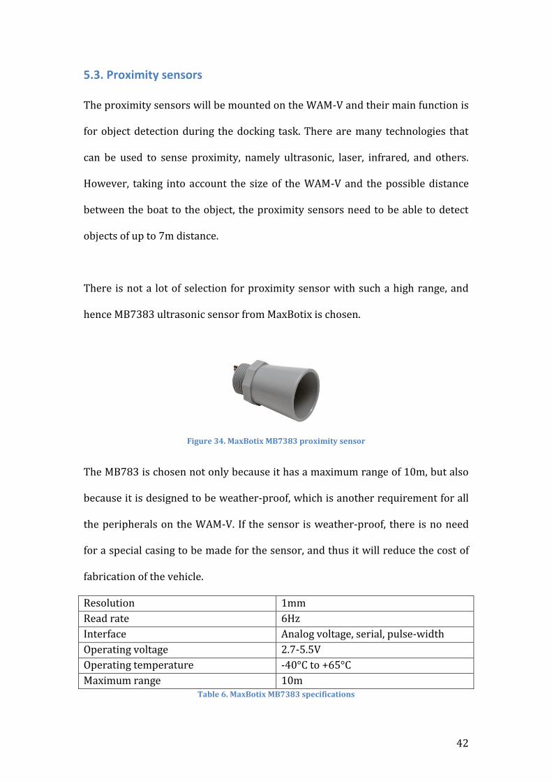
hence MB7383 ultrasonic sensor from MaxBotix is chosen.
Figure 34. MaxBotix MB7383 proximity sensor
The MB783 is chosen not only because it has a maximum range of 10m, but also
because it is designed to be weather-proof, which is another requirement for all
the peripherals on the WAM-V. If the sensor is weather-proof, there is no need
for a special casing to be made for the sensor, and thus it will reduce the cost of
fabrication of the vehicle.
Resolution 1mm Read rate 6Hz Interface Analog voltage, serial, pulse-width Operating voltage 2.7-5.5V Operating temperature -40°C to +65°C Maximum range 10m
Table 6. MaxBotix MB7383 specifications

43
6 ASV Electronics Board
To interface with the electronics peripherals, the ASV will need a custom
electronics board with the main functions such as:
- Power distribution
- Data connectivity distribution between the SBC and peripherals
- Sensors and motors interface
As such, some of the features of the ASV electronics board are similar to those of
the AUV backplane, but there will be additional ones, such as the interface with
batteries and motors.
6.1. Soft start
The soft-start capability is similar with the one described in section 4.2., with the
new values for the resistor and capacitor set.
Figure 35. N-channel MOSFET based soft-start circuit
The RC filter from R1 and C1 provides an RC filter that will cause a delay before
the gate of the MOSFET is open and power is given to the load. This prevents
inrush current from happening.

44
6.2. Load sharing capability
In the Bumblebee AUV 3.0, to balance the two batteries for the electronics, there
is a need to balance the load drawn from each of the battery. As such, a load
sharing circuit is implemented using power path switcher IC LTC4416 from
Linear Technology. When the difference between the two input sources is more
than 100mV, the IC will control a P-MOSFET such that the load will draw current
from the battery with the higher voltage.
Figure 36. Load-sharing circuit using LTC4416
Similar circuit is implemented on the ASV electronics board to balance the two
batteries powering the electrical peripherals in the ASV.
6.3. UART to RS485 converter
The battery for the thrusters, Torqeedo Power 26-104, uses RS485 connection to
disclose the battery information. To allow the MCU in the electronics board to
monitor the battery status, a UART to RS485 converter circuitry is needed.
For this, RS485 transceiver IC, MAX485 from Maxim Integrated is used.

45
Figure 37. Typical half-duplex RS485 network (Maxim Integration)
Figure 37 shows how four MAX485 ICs can be used to connect UART devices to
join in the RS485 network. In the ASV application, there is only one IC needed for
the communication with the battery. If Torqeedo Cruise 2.0R thrusters are going
to be used, two more MAX485 ICs are needed for the communication to control
each of the thrusters.
A breadboard prototype was done with a setup using Arduino to send UART
messages through the MAX485 IC, and the RS485 output is connected to a RS485
to USB converter cable from FTDI to be fed into a computer. The computer
manages to receive the UART message from Arduino.
6.4. Power over Ethernet (POE) injector
The LIDAR, GigE cameras, and the acoustics sub-system are located outside of
the main hull, and they interface with the main processing unit through POE. POE
uses RJ45 Ethernet cable to transfer both data and power to the devices. Figure
38 shows the pin allocation for the implementation of POE on the RJ45 cable.

46
Figure 38. Pin allocation for POE on RJ45 cable (www.wisptech.com)
10Mbps Ethernet only uses two pairs of twisted-pair wire to transmit the data. In
other words, out of the four twisted-pair wires inside the RJ45 cable, two of them
are not used at all. POE uses those unused pair of wires to transmit Power and
Ground, so that power and data can be transmitted using one RJ45 cable.
The POE injector has been working well in the Bumblebee AUV backplane to
interface with the imaging sonar and other sub-systems.
Figure 39. Stacked RJ45 connector for POE injector (www.global-sources .com)
47
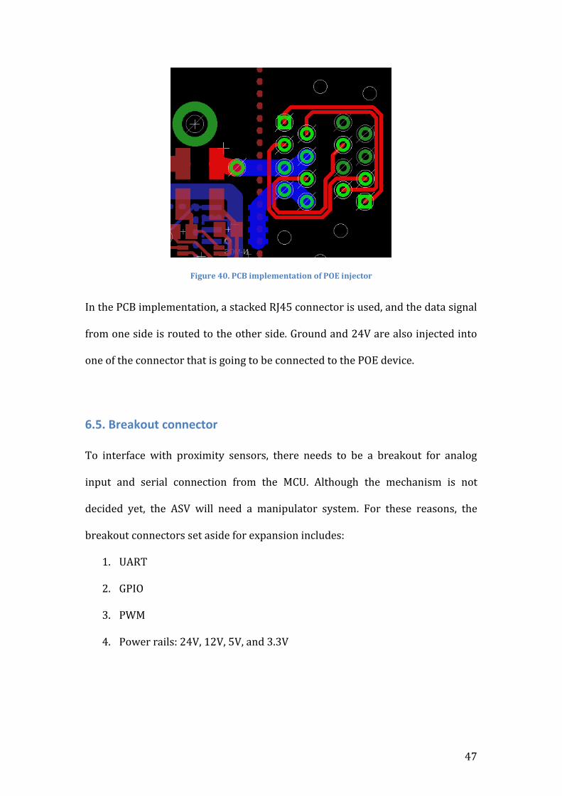
Figure 40. PCB implementation of POE injector
In the PCB implementation, a stacked RJ45 connector is used, and the data signal
from one side is routed to the other side. Ground and 24V are also injected into
one of the connector that is going to be connected to the POE device.
6.5. Breakout connector
To interface with proximity sensors, there needs to be a breakout for analog
input and serial connection from the MCU. Although the mechanism is not
decided yet, the ASV will need a manipulator system. For these reasons, the
breakout connectors set aside for expansion includes:
1. UART
2. GPIO
3. PWM
4. Power rails: 24V, 12V, 5V, and 3.3V

48
7 ASV Electronics Boards
Figure 41. Power and data links between the electronics board and the other ASV components
Figure 41 shows the power and data links between the electronics board and the
different peripherals across the vehicle. Inside the same housing as the board, it
will provide power for the SBC, Ethernet switch, and the USB hub. Outside the
main housing, the board will provide power and data connectivity to the rest of
the peripherals in the diagram.

49
Figure 42. ASV electronics board architecture
Figure 42 shows the architecture of the electronics board. The MCU as main
processor of the board will manage the data connectivity to the battery,
thrusters, and sensors.

50
8 ASV Electrical Architecture
Figure 43. ASV data connectivity architecture
Figure 44. ASV power architecture

51
The ASV will have two different power sources: the 26V/104Ah battery for the
thrusters, and the 24V/7.8Ah battery for the other peripherals, such as the SBC
and the sensors. As such, the noise from the thrusters will not affect sensitive
electronic components.
For data connectivity, the SBC as the main processing unit interfaces with a
LIDAR device, two Gigabit Ethernet (GigE) cameras, and the acoustics sub-
system through Ethernet connection. It will also provide FireWire interface for a
stereo camera. The communication to the Inertial Measurement Unit (IMU) and
the WiFi receiver is through USB connection.
The electrical backplane will receive data through RS485 protocol from the
battery and the thrusters (for Torqeedo Cruise 2.0R) or Pulse Width Modulation
(PWM) signal (for MinnKota RT80), and through TTL level UART for the
proximity sensors and Power Monitoring Board (PMB). These data will then be
processed by the MCU on board and passed on to the SBC through UART
connection.
9 Conclusion
The implementation of a backplane on an AUV shows the importance of a custom
board to distribute power and to manage different communication protocols
across the sub-systems. Compared to distributing power using cables, it
minimizes the possibility of mechanical failure of cabling.
52
Unfortunately due to the delay in funding, the expensive ASV peripherals such as
the battery and the thrusters are not bought yet, and thus the electronics board
designed is not tested with the real devices yet. Undoubtedly there will be
problems that will come up during deployment and thus it is important to
reiterate the design even after fabrication and testing.
References
Albright, G., Edie, J., & Al-Hallaj, S. (2012). A Comparison of Lead Acid to Lithium-ion in Stationary Storage Applications. Retrieved from http://www.altenergymag.com/content.php?post_type=1884 Anderson, M. (2014). Model-based Control and Control Allocation System for a Wave Adaptive Modular Vessel. Retrieved from https://wiki.csem.flinders.edu.au/pub/CSEMThesisProjects/ProjectAnde0455/Thesis.pdf Electronics, W. (2012). ABC of Power Module. Wurth Electronics. FTDI. (2013). USB Hardware Design Guidelines for FTDI ICs. Retrieved from http://www.ftdichip.com/Support/Documents/AppNotes/AN_146_USB_Hardware_Design_Guidelines_for_FTDI_ICs.pdf Intel. (2000). High Speed USB Platform Design Guidelines. Retrieved from http://www.usb.org/developers/docs/hs_usb_pdg_r1_0.pdf Jones, G. (2005). Miniature solutions for voltage isolation. Retrieved from http://www.ti.com/lit/an/slyt211/slyt211.pdf Kularatna, N. (1998). Power Electronics Design Handbook. Newnes. Montrose, M. (2000). Printed Circuit Board Design Techniques for EMC Compliance. Wiley-IEEE. Semtech. (2003). TVS Diode Application Note. Retrieved from https://www.semtech.com/images/datasheet/si99-01.pdf Texas Instruments. (2012, March). MSP430™ System-Level ESD Considerations. Retrieved from http://www.ti.com/lit/an/slaa530/slaa530.pdf Texas Insruments. (2015). High-Speed Interface Layout Guidelines. Retrieved from http://www.ti.com/lit/an/spraar7e/spraar7e.pdf

53
Witherspoon, B. (2008). Voltage Regulation using Zener Diodes. Retrieved from http://www.egr.msu.edu/classes/ece480/capstone/fall08/group03/appnotes/files/zener_shunt_regulator.pdf Wuidart, L. Topologies for Switched Mode Power Supplies. ST Electronics.