electrical control equipment for the continuous...
TRANSCRIPT

Electrical control equipment for thecontinuous copper casting rod plant
Item Type text; Thesis-Reproduction (electronic)
Authors Glickman, Steven, 1949-
Publisher The University of Arizona.
Rights Copyright © is held by the author. Digital access to this materialis made possible by the University Libraries, University of Arizona.Further transmission, reproduction or presentation (such aspublic display or performance) of protected items is prohibitedexcept with permission of the author.
Download date 20/06/2018 00:47:41
Link to Item http://hdl.handle.net/10150/554871
ELECTRICAL CONTROL EQUIPMENT FOR THE CONTINUOUS COPPER CASTING ROD PLANT
bySteven Glickman
A Thesis Submitted to the Faculty of theDEPARTMENT OF ELECTRICAL ENGINEERING
In Partial Fulfillment of the Requirements For the Degree ofMASTER OF SCIENCE
In the Graduate College
THE UNIVERSITY OF ARIZONA
1 9 7 5

STATEMENT BY AUTHOR
This thesis has been submitted in partial fulfillment of requirements for an advanced degree at The University of Arizona and is deposited in the University Library to be made available to borrowers under rules of the Library.
Brief quotations from this thesis are allowable without special permission, provided that accurate acknowledgment of source is made. Requests for permission for extended quotation from or reproduction of this manuscript in whole or in part may be granted by the head of the major department or the Dean of the Graduate College when in his judgment the proposed use of the material is in the interests of scholarship. In all other instances, however, permission must be obtained from the author.
SIGNED: V
APPROVAL BY THESIS DIRECTOR
This thesis has been approved on the date shown below:
Professor of Electrical Engineering

ACKNOWLEDGMENTS ^
Sincere thanks must be extended to Mr. Warren Hawes of Magma Copper Company and to Dr. Robert N. Carlile for coordinating the internship summer work program leading to the preparation of this thesis.
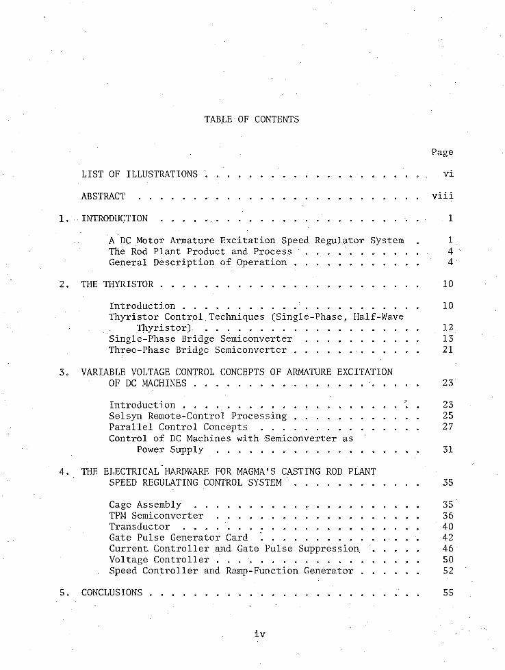
TABLE OF CONTENTS
Page
LIST OF ILLUSTRATIONS . . . . . . . . . . . . . . . . . . . . . vi
ABSTRACT .............. viii
1. INTRODUCTION ......... 1A DC Motor Armature Excitation Speed Regulator System . 1The Rod Plant Product and Process . . . . . . . . . . . 4General Description of Operation . .......... 4
2. THE THYRISTOR.................. 10Introduction . . . . . . . . . . . .......... 10Thyristor Control Techniques (Single-Phase, Half-Wave
Thyristor) . . . .......... 12Single-Phase Bridge Semiconverter .............. 13Three-Phase Bridge Semiconverter . . . . . ......... 21
3. VARIABLE VOLTAGE CONTROL CONCEPTS OF ARMATURE EXCITATIONOF DC MACHINES ........................ 23Introduction . . . " . . 23Selsyn Remote-Control Processing . .................... 25Parallel Control Concepts . 27Control of DC Machines with Semiconverter as
Power S u p p l y .............. 314. THE ELECTRICAL HARDWARE FOR MAGMA'S CASTING ROD PLANT
SPEED REGULATING CONTROL SYSTEM . . . . . . . . . . . . 35
Cage A s s e m b l y ................ 35TPM Semiconverter . .......................... 36Transductor . . . . . . . . . . .......... . ........ 40Gate Pulse Generator Card . . . .............. 42Current Controller and Gate Pulse Suppression . . . . 46Voltage Controller . 50Speed Controller and Ramp-Function Generator ........ 52
5. CONCLUSIONS .......... 55
iv

V
TABLE OF CONTENTS--Continued
Page
APPENDIX A - A DERIVATION FOR THE AVERAGE LOAD VOLTAGE VS.FIRING ANGLE FOR A THREE-PHASE THYRISTORSUPPLY . . . . . . . . . . .................... 56
REFERENCES 59

LIST OF ILLUSTRATIONS
Figure Page
1.1 Block Diagram of Armature Speed Regulator . . . . . . . . . 21.2 DC Single Line Diagram . ............................... 5
2.1 Thyristor Circuit Symbol ..........• 11
2.2 Static Characteristics of Thyristor . ................... 112.3 Single-Phase Control Circuit . . . . ..................... 122.4 Voltage and Current Waveforms in a Single Phase Thyristor-
Controlled Circuit with Resistive Load .......... 142.5 Operation of Single-Phase Thyristor Control Circuit into
and Inductive Load .................. 152.6 Single-Phase Semiconductor with Free-Wheeling Diode . . . . 16
2.7 Waveforms of Supply Load Voltage, and Trigger Pulses fora Single-Phase Bridge Semiconverter ........... . . . . 17
2.8 Waveforms for Semiconverter Bridge with Complex Load . . . 19
2.9 Load Current Waveform with Free-Wheeling Diode . . . . . . 202.10 Three-Phase Bridge Semiconverter . . . . . . . . . . . . . 212.11 Waveforms for a Three-Phase Semiconverter . . . .......... 22
3.1 Closed-Loop DC Motor Speed-Control System . . . .......... 24
3.2 Single-Phase Synchrotransmitter Motor . . . . . . . . . . . 263.3 Synchro Geherator-Transformer S y s t e m ........ . ........ 263.4 Parallel Drive Control ........ . . . . . . 28
3.5 Switching Circuit........ 29
3.6 Operational Amplifier Circuit for Control of Speed withCurrent Reference Limit . . . . . . . 30
vi
v n
LIST OF ILLUSTRATIONS--Continued
Figure Page
3.7 Machine Control with Semiconverter Power Supply . ........ 323.8 DC Machine Control with Additional Voltage Feedback . . . . 34
4.1 Zener Regulators and Filters . . . .......... 374.2 Isolation Transformer, Voltage Feedback Loop, and Gate
Pulse Generation Card for a Thyristor Power Module . . . 38
4.3 Thyristor Power Module Semiconverter .............. 394.4 Calibration Curve of Typical DC Current Transformer . . . . 41
4.5 DC Current Sensing Circuit . ................ 424.6 Gate Pulse Generator Circuit ............................. 44
4.7 Voltage Waveforms of Thyristor, Capacitor, TransistorInput, and Trigger Pulses .................... 45
4.8 Transfer Curve of V^n vs. a . . . .............. 474.9 Current Controller and Gate Pulse Suppression . ........ 48
4.10 Voltage Controller.............. 51
4.11 Speed Controller and Ramp Function Generator .......... 53
A.l Average Load Voltage vs. Firing Angle .................... 58
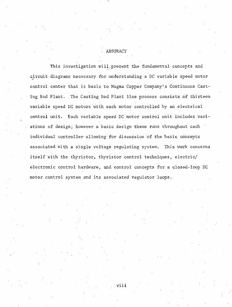
ABSTRACT
This investigation will present the fundamental concepts and
circuit diagrams necessary for understanding a DC variable speed motor control center that is basic to Magma Copper Company's Continuous Cast
ing Rod Plant. The Casting Rod Plant line process consists of thirteen variable speed DC motors with each motor controlled by an electrical control unit. Each variable speed DC motor control unit includes variations of design; however a basic design theme runs throughout each
individual controller allowing for discussion of the basic concepts associated with a single voltage regulating system. This work concerns
itself with the thyristor, thyristor control techniques, electric/
electronic control hardware, and control concepts for a closed-loop DC
motor control system and its associated regulator loops.
viii
CHAPTER I
INTRODUCTION
A DC Motor Armature Excitation Speed Regulator System
This work presents the basic control concepts; electrical/ electronic hardware, and schematic diagrams required for a typical DC motor speed regulator system used in the mill and coiling drive sections
of the Continuous Copper Casting Rod Plant built for Magma Copper
Company, San Manuel, Arizona.The armature excitation speed regulator discussed in this paper
and common to each individual motor control system used in the casting rod plant is represented in block diagram form in Figure 1.1. This
diagram indicates the basic flow of control needed for the adjustment
of machine speed. A brief introductory discussion of the components
shown in the blocks follows, with a detailed analysis of electrical/ electronic hardware given in subsequent chapters.
The thyristor power supply consists of a rectifier assembly which is capable of delivering adjustable levels of direct voltage to
the armature of the motor. The operation of this type of assembly will be discussed extensively in Chapter 2. The gate pulse generator, a
solid state "firing" circuit, represents the control circuit which ad
justs the thyristor supply voltage level to that desired for proper
1

2LEGEND FDR FUNCTION pLQCKS
T IT L E U-VOLTAGE Sf^SOR
uINPUT).OLrrPi/T VARIABLE inpltt v a r ia b l e QUyVT
GAIN CURVE
TIME RESPONSE TO STEP IN P U T
L E fe U D FOR POWER C IR C U IT
L-CH5cMOTOR 'Nx.c.
SEMICONVERTER CIRCUIT
C U R R E N T X fO R M F R
POWER SOURCE
frrso ootrnxuLZ/r
GW/*jsC GS/*rx'*rBt>voiTAor eofsr/ooiic/?
rjrAwsDovTOV
ci*%wvr covnpoi i r#
VV
Gyrrr fn/isr s'i/*wrs&/ov
Figure 1.1. Block Diagram of Armature Speed Regulator. (Courtesy of Westinghouse Electric Corporation.)
machine speed. The "firing" control technique is introduced in Chapter 2, and a gate pulse generator circuit schematic is explained in Chapter 4. The speed controller function is to compare a desired speed
reference setting to that of a speed feedback signal, producing an error signal indicating that the power conversion equipment (the thyristor power supply) needs an output voltage correction. The speed controller is introduced in Chapter 3, with the circuit diagram explained in Chapter 4. The generator tachometer is direct coupled to the motor and
measures the angular velocity of the shaft, producing a speed feedback signal proportional to the motor speed. The tachometer generator will not be considered any further. The voltage controller is a time delay amplifier which has large signal gain. The voltage controller signal
provides the input to the gate pulse generator, which initiates the
control of the DC voltage output of the thyristor power supply as brief
ly mentioned earlier. The voltage controller is introduced in Chapter 3
and its circuit diagram will be explained in Chapter 4. The current controller function is to protect the equipment from excessive overloads
This is achieved by comparing a current feedback signal to the current
reference setting limit. If there is a current overload beyond the limit reference setting, the current controller will slow down the drive
system. If the current becomes excessive, gate pulse suppression will
be triggered, causing the system to shut-down altogether. The current controller is introduced in Chapter 3, with the circuit diagram explained in Chapter 4. The current feedback signal is developed by the
transductor, which converts a DC current flow into a corresponding
voltage signal level. The circuit diagram for the transductor is shown
in Chapter 4.
The Rod Plant Product and Process
The operation of the Casting Plant involves taking refined cathode copper from the refinery, melting the cathodes in a gas-fired furnace and feeding the molten copper to an eight-foot casting wheel.The casting wheel forms a square bar which is fed through a rolling mill operation. . The twelve stands of the rolling mill form a 5/16-inch diameter copper rod. After leaving the rolling mill the rod is treated
with a dilute sulfuric acid, rinsed, coated, and finally wound into
coils of various sizes, 8,000 to 16,000 pounds. The coils are checked-, weighed on highly accurate scales and then loaded into railroad cars or trucks.
In the past Magma's copper was shipped in the form of copper
anodes to out-of-state refineries for processing. Now the entire pro
duction process takes place at San Manuel. This production has met the
growing demand for refined copper from western manufacturers of electrical equipment and wire products.
General Description of Operation
The following description which introduces the line process
relates to the single-line diagrams included in Figures 1.2a,b,c. The operation begins with refined copper cathodes of 99.98% purity being
loaded into a gas-fired melting furnace. Once heated, the molten copper

to hill m r x YP/HSMACXlcxmcrop
P/yVCM POLL S*P
AuroMILL SP°' -"1 (cAy/f cc/imk)
<FHD & --& —
mi s/rro | rtPwee r ~~Z Cm u crstr) rv *
ED Lr-
i—
<•->
Figure 1.2. DC Single Line Diagram. (a) Casting Wheel Section.(Courtesty of Westinghouse Electric Corporation.)

8 8 0 8h / i l f r s r e r m > ./ ato. z m o 3P i n c h p o l l ss /m M / t t . s -f/tc
7 5 H P /5 0 H P /S O H P /S O H P
rCZ3A/O. 4 AfUt
/ S O H P
PCF
r-lDsnu>y e e )~CT ■z.ouro
MIL P/.tpyP / A / ( H r CL L r.-'S *
NO /
DAM.ZSHfPP 2 0 HP
A” loo><£-I
. ro P/N/P/i/A/f A T I L L
6N O . Z L O O P S t L S Y A f
S f L S Y s JO/MOC-OLPTOP
M . Z P f f L L ,
N O S M I L L ,AMD
N O 4 M I L L
A P £
d u p l i c a t e
T O
M O J M I L L
AUTO
SPY CD
U\ EDAoroi:
XT X AO. 2
LOOP rUNNt*
~PNO ~PCD
CZPCV ElPtVD
NO- ZSHEAR
Figure 1.2.--Continued. (b) Roughing Mill Section.

x-Z/t/ZT/V/ Sf/M zxacot/fi
SrAMDCAL.OOTS
LOAD
S3 r
A/O.Z
Figure 1.2.--Continued. (c) Finishing Mill and Coiler Sections.
flows from the melting furnace at a temperature of 2100°F to a 15-ton holding furnace. The holding furnace has an adjustable tilt angle which
allows for varying pour rates of the molten copper being fed to the
96-inch diameter casting wheel. A typical pouring rate would be approx
imately 30-tons per hour. The molten copper being fed to the casting wheel and band passes through water cooling sprays, forming a continuously cast copper bar five inches square with a tempterature of 1400°F.Upon leaving the casting wheel the bar will be moving at 60' feet per minute and guided by an extractor conveyor and extractor pinch rolls.The bar is next fed through the No. 1 crop and cobble shear, which cuts off the initial undertemperature front end until a satisfactory temper
ature is reached, and then is fed through a downlooper table and No. 1
dowhlooper. After passing through the downlooper the bar enters a preparation unit which chamfers the edges and brushes off bar surface
scale.The bar is then fed into the mill entry pinch rolls, which close
over the bar and deliver it to the first of four roughing mill stand
sections. The no-twist roughing mill consists of four alternate hori
zontal and vertical mill stands with each stand driven by 150 HP DC motor. The four roughing stands alternately pinch or squeeze the bar
into alternate oval and round shapes,, reducing its diameter until forming a round stock approximately one inch in diameter traveling with a speed of 300 feet per minute.
The round stock is fed to the No. 2 crop and cobble shear, which.once again crops the front end of the bar until a satisfactory
temperature is achieved for entry into the finishing mill. From the
No. 2 shear the stock passes over the second downlooper table through the No. 2 loop selsyn into the no-twist finishing mill. The finishing mill is similar to the roughing mill but consists of eight alternate horizontal and vertical mill stands driven by two direct-coupled 800 HP
DC motors.The round stock, having passed through the finishing mill, has
been reduced in diameter, forming a 5/16-inch solid copper rod with a speed of 3000-3500 feet per minute. The rod then passes through a dilute sulfuric pickling acid solution station where the surface is
cleaned and treated and also passes through a final station where it isrinsed and waxed to prevent further oxidation.
The rod is next directed through a delivery pipe by a pair of
coiler pinch rolls to the rod coiler. The rod coiler head consists
essentially of a section of curved rotating or spinning pipe through
which the rod passes. The coiler forms a product such that the rings
of rod are coiled and laid on a pallet positioned underneath the coiler.
Upon completion of a coil the loaded pallet is pushed out from under the
coiler and replaced by an empty pallet. During the coiL change-out period, the rod rings being continuously formed by the spinner are temporarily collected by the coil collector fins.
CHAPTER 2
THE THYRISTOR
Introduction
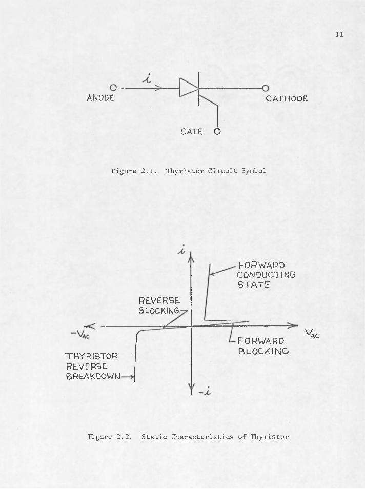
The thyristor is a three-terminal four-layer p-n-p-n semiconductor device which operates as a controlled rectifier. Its electric
circuit symbol is shown in Figure 2.1. Essentially the device is a switch, which remains off or appears to have an infinite input impedance
until the device has been "triggered.When both the anode and gate terminals have the proper positive voltages with respect to the cathode
terminal the thyristor switches on, and current flows and will continue to flow without further gate signals. Ideally the thyristor has no impedance when conducting. To switch the device off, the gate signal
must be removed and the anode current must be reduced to zero. Like a rectifier diode, the thyristor allows current flow in only one direction.
The static characteristics of a typical thyristor for both the conducting and non-conducting states are shown in Figure 2.2. With a
reverse voltage applied to the thyristor, the voltage current characteristic is similar to that of a diode with a small reverse current being
produced by a reverse voltage until an avalanche region is reached. If
the thyristor is not triggered in the forward direction a small forward
current is produced until the forward avalanche region is reached and
the characteristic changes to the conducting-state characteristic. The
11
ANODE CATHODE
GATE 6
Figure 2.1. Thyristor Circuit Symbol
■ FORWARDCONDUCTINGSTA TE
REVERSEBLOCKING
FORWARDBLOCKINGTHYRISTOR
REVERSEBREAKDOWN
VAC
Figure 2.2. Static Characteristics of Thyristor
12
conducting-state characteristic obtained from the thyristor when triggered is similar to that of a diode with a forward voltage applied.
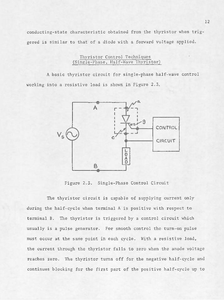
Thyristor Control Techniques (Single-Phase, Half-Wave Thyristor)
A basic thyristor circuit for single-phase half-wave control
working into a resistive load is shown in Figure 2.3.
r -
CONTROL
CIRCUIT
Figure 2.3. Single-Phase Control Circuit
The thyristor circuit is capable of supplying current only
during the half-cycle when terminal A is positive with respect to
terminal B. The thyristor is triggered by a control circuit which
usually is a pulse generator. For smooth control the turn-on pulse
must occur at the same point in each cycle. With a resistive load,
the current through the thyristor falls to zero when the anode voltage
reaches zero. The thyristor turns off for the negative half-cycle and
continues blocking for the first part of the positive half-cycle up to
13
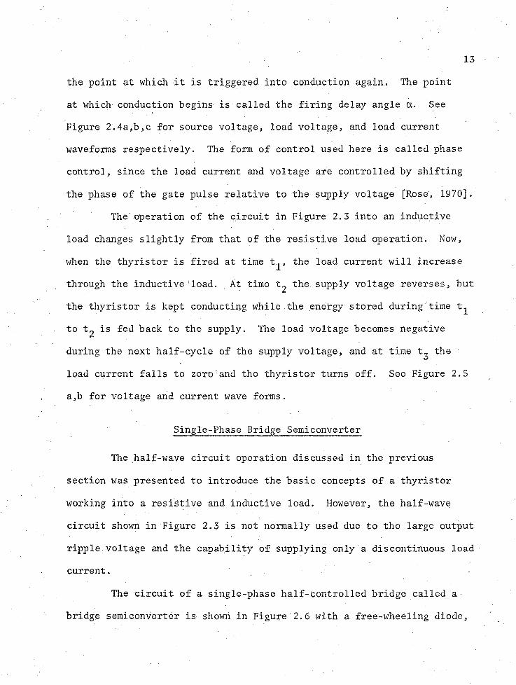
the point at which it is triggered into conduction again. The point
at which conduction begins is called the firing delay angle a. See Figure 2.4a,b,c for source voltage, load voltage, and load current waveforms respectively. The form of control used here is called phase control, since the load current and voltage are controlled by shifting
the phase of the gate pulse relative to the supply voltage [Rose, 1970].The operation of the circuit in Figure 2.3 into an inductive
load changes slightly from that of the resistive load operation. Now,
when the thyristor is fired at time t^, the load current will increase
through the inductive load. At time t^ the supply voltage reverses, but the thyristor is kept conducting while the energy stored during time t^
to tg is fed back to the supply. The load voltage becomes negative during the next half-cycle of the supply voltage, and at time t^ the
load current falls to zero'and the thyristor turns off. See Figure 2.5 a,b for voltage and current wave forms.
Single-Phase Bridge Semiconverter
The half-wave circuit operation discussed in the previous
section was presented to introduce the basic concepts of a thyristor
working into a resistive and inductive load. However, the half-wave
circuit shown in Figure 2.3 is not normally used due to the large output
ripple voltage and the capability of supplying only a discontinuous load current.
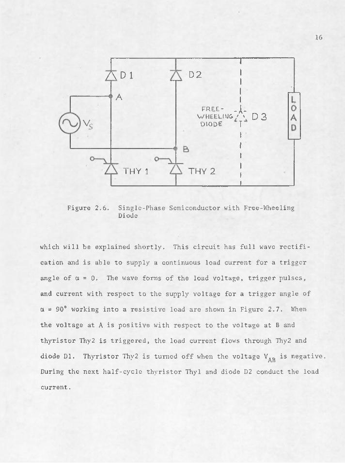
The circuit of a single-phase half-controlled bridge called a
bridge semiconverter is shown in Figure 2.6 with a free-wheeling diode.

14
(a)
(b)
-cx
( C )
oc
Figure 2.4. Voltage and Current Waveforms in a Single Phase Thyristor-Controlled Circuit with Resistive Load

15
L 4
(a)
SUPPLY f THYRISTORc u r r e n t
(b)
Figure 2.5. Operation of Single-Phase Thyristor Control Circuit into an Inductive Load
16
ADI4 a
D 2
FREE- _X_ WHEELING ' \ D 3
DIODE JV c
THY 1 THY 2
Figure 2.6. Single-Phase Semiconductor with Free-Wheeling Diode
which will be explained shortly. This circuit has full wave rectifi
cation and is able to supply a continuous load current for a trigger
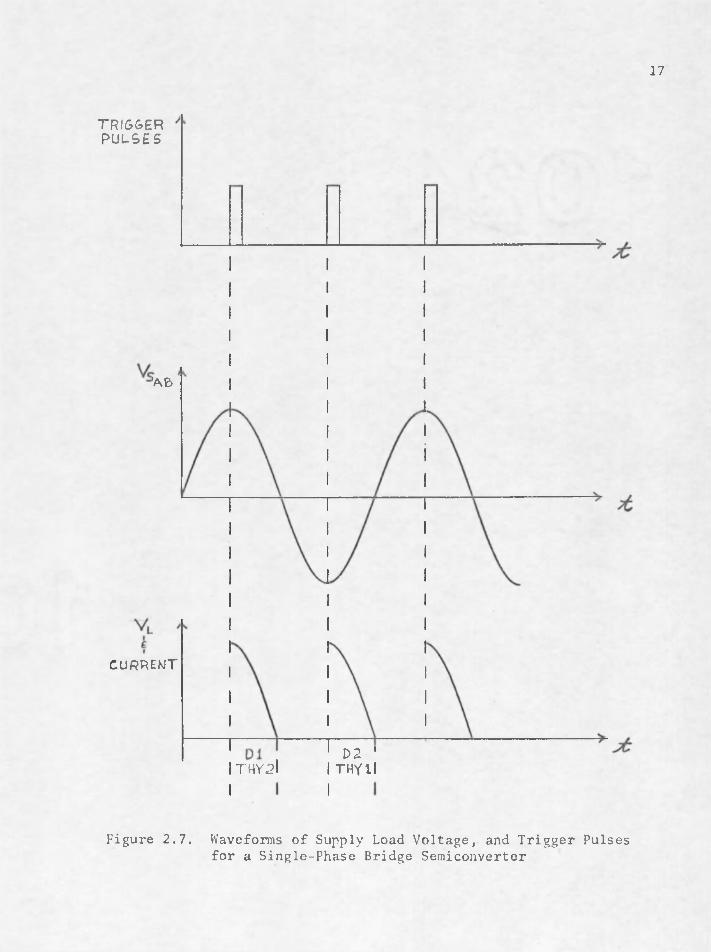
angle of a = 0. The wave forms of the load voltage, trigger pulses, and current with respect to the supply voltage for a trigger angle of
a = 90° working into a resistive load are shown in Figure 2.7. When
the voltage at A is positive with respect to the voltage at B and thyristor Thy2 is triggered, the load current flows through Thy2 and diode Dl. Thyristor Thy2 is turned off when the voltage V^B is negative. During the next half-cycle thyristor Thyl and diode D2 conduct the load current.
17
TRIGGERPULSES
'A 6
CURRENT
D2 1 THYllTHY2I
Figure 2.7. Waveforms of Supply Load Voltage, and Trigger Pulses for a Single-Phase Bridge Semiconverter
18
The operation of the bridge circuit for a complex load, repre
senting the inductance of a motor, is considered next. The wave forms and current in relation to the supply voltage are shown in Figure 2.8.
At the end of each half-cycle of the supply voltage, currentflow is maintained in the circuit by the inductance of the load. Thethyristor which has been firing, say Thy2, continues to conduct but transfers current from diode D1 to diode D2 so that the load inductive stored energy continues to drive current through the bridge without
including the reverse supply voltage. During this part of the cycle,load current decays exponentially and is unaffected by the supply
voltage. When thyristor Thyl is triggered, thyristor Thy2 is reversed bias by the supply voltage and turns off. Current now flows from the source through thyristor Thyl and diode D2 into the load. Thyristor Thy2 is triggered in the next half-cycle and the sequence is repeated.
The load current can be controlled by changing the trigger
angle a of the thyristor. One limitation, however, is that it may notbe possible to turn off the load current even when not triggering the
thyristors. Let us consider how that may happen. If a trigger pulse is removed immediately after the firing of a thyristor, it will continueto conduct for the remaining half-cycle of the supply. If the other
thyristor receives no trigger pulse it will not turn on. However, if
the load is highly inductive, with a time constant greater than one
half-cycle, the first thyristor will still be conducting at the end of this period and will remain turned on for the following half-cycle. The circuit will continue to operate thi s way indefinitely.

19
TRI66ERPULSES
5 U PPLY IOUTPUTVOLTAGES BRIDGE OUTPUT
V THYRISTORS FULLY \ COND0CT(NG>
- SUPPLY V 0 L 7A 6 E
FORWARD VOLTA6E DROP OF t t \y r \STOR AMD D\ODE
L O A DCURRENT
THY 1| THY^ THY2J THYll TH Y i IW 21 FHY<?| C ON D UCT | K) C,m i m i 07 i n? i IM i m i rs7 i DEVICES
Figure 2.8. Waveforms for Semiconverter Bridge with Complex Load

20
If a free-wheeling diode is added to the half-controlled bridge, as shown in Figure 2.6, the load current is transferred to the free-wheeling diode at the end of each half-cycle of the supply
[Mazda, 1973]. The load current waveform for a complex load shown in Figure 2.9 is similar to those of the half-controlled bridge without a free wheeling diode, but the exponential decay part of the load current
is now carried by the free-wheeling diode D3. The addition of the freewheeling diode ensures that each thyristor turns off at the end of each half-cycle, so there is no risk of conduction carrying over into the next half-cycle. The load current then will always be under the control
of the trigger circuit.
LOADCURRENT
TMY2THY 1
D 2D3 CONDUCTING
DEVICES
Figure 2.9. Load Current Waveform with Free-Wheeling Diode

21
Three-Phase Bridge Semiconverter A solid-state three-phase bridge semiconverter circuit is shown
in Figure 2.10. The top half of the circuit is controlled so that conduction will occur from the most positive phase in which a thyristor has been connected. The current in the bottom of the bridge will commutate from one diode to the next depending on which is connected to the most negative phase. Figure 2.11 shows the supply and load volt
ages.
THREE-P H A S ESUPPLY
0 - v L ° ~ Y _ ° ~ V _7 \ THY 1 A TH Y 2 A T H Y 3
A d i A D2 A d 2>
Figure 2.10. Three-Phase Bridge Semiconverter

22
c o n t r o l l e dTHYRISTORs
PHASEVOLTAGEZ \
Figure 2.11. Waveforms for a Three-Phase Semiconverter
CHAPTER 3
• VARIABLE VOLTAGE CONTROL CONCEPTS OF ARMATURE EXCITATION OF DC MACHINES
Introduction ;
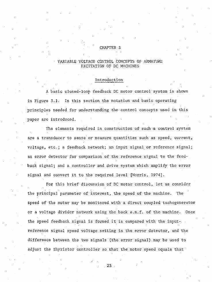
A basic closed-loop feedback DC motor control system is.shown
in Figure 3.1. In this section the notation and basic operating principles needed for understanding the control concepts used in this
paper are introduced.The elements required in construction of such -a control system
are a transducer to sense or measure quantities such as speed, current,
voltage, etc.; a feedback network; ,an input signal or reference signal;
an error detector for comparison of the reference signal to the feedback signal; and a controller and drive system which amplify the error
signal and convert it to the required level [Morris, 1974].For this brief discussion of DC motor control, let us consider
the principal parameter of interest, the speed of the machine. The speed of the motor may be monitored with a direct coupled tachogenerator
or a voltage divider network using the back e.m.f. of the machine. Once
the speed feedback signal is formed it is compared with the input- reference signal speed voltage setting in the error detector, and the
difference between the two signals (the error signal) may be used to
adjust the thyristor controller so that the motor speed equals that
23
REFERENCE INPUT
SIGNAL O
ERRORSIGNAL
POWER I INPUT I
THYRISTOR CO NTROLLER
AND DRIVE
MEASUREMENT DEVICE
MOTOR
FEEDBACK SIGNAL X
Figure 3.1. Closed-Loop DC Motor Speed-Control System

. ' 25 demanded by the input reference signal. It is the principal functionof the error signal to control the flow of power through the thyristorcontroller to the DC motor and hence adjust the motor speed to thatdesired.
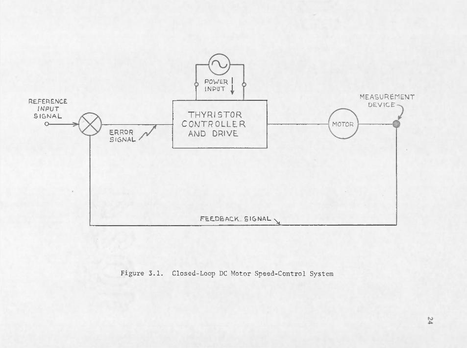
Selsyn Remote-Control Processing
Another important control device used in the continuous casting
rod plant is the servomechanism. Specifically of interest are selsyns (or synchros), electromagnetic devices used primarily for the transfer of angular-position information. One is operated at the sending point
as a generator and is called the transmitter, the other is operated at the receiving point as a motor and is called the receiver, shown in Figure 3.2. Selsyns are, in effect, transformers whose primary to
secondary coupling may be changed by varying the relative position of
the two windings. The single-phase winding current in the primary
induces voltages in the three windings of the secondary. These three voltages are not equal in magnitude, but vary with the position of the
rotor. When the two rotors correspond in position relative to the stators, the voltages induced in the transmitter secondary are equal to those induced in the receiver secondary. The voltages are therefore
balanced and no current flows in the secondary windings. If the trans
mitter rotor position is changed, the induced voltages are no longer equal and current flows in the secondary windings. This current with
the magnetic fields produces a torque which turns the receiver rotor to
a new balanced voltage position. Thus, as the transmitter is turned the receiver follows at the same speed and direction.
26
RECEIVERTRANSM ITTERSECONDARY
R O T O RPRIMARY ROTOR
STATORSTATOR
Figure 3.2. Single-Phase Synchrotransmitter Motor
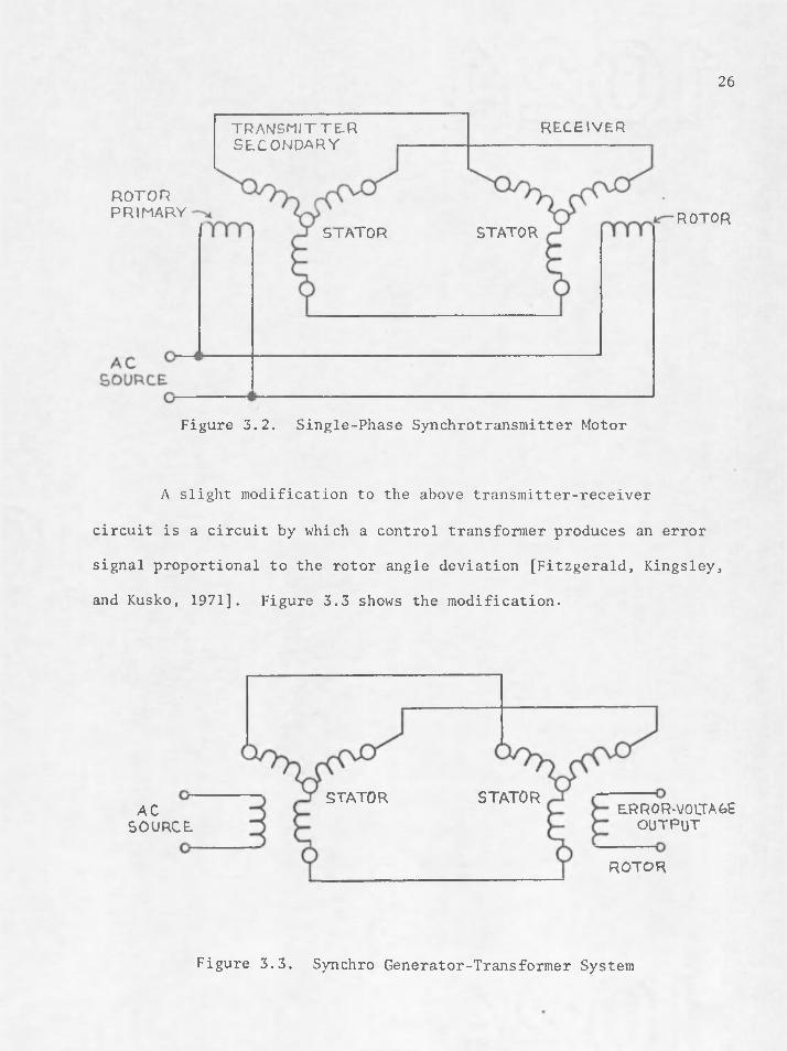
A slight modification to the above transmitter-receiver
circuit is a circuit by which a control transformer produces an error signal proportional to the rotor angle deviation [Fitzgerald, Kingsley, and Kusko, 1971]. Figure 3.3 shows the modification.
STATORSTATOR ERR0R-V01TAGEOUTPUT
ACSOURCE
ROTOR
Figure 3.3. Synchro Generator-Transformer System
27
Down-looper regulators No. 1 and 2 consist of the synchro generator-transformer system as just described. These down-loopers were referred to earlier in Chapter 1 and may be seen in Figure 1.2a,b.
These remote position sensors have the function of developing a correction speed signal maintaining the bar free of tension. Let us consider the No. 1 looper arm. The No. 1 looper is located ahead of
the mill entry pinch roll and develops a correction speed reference signal for the entry pinch roll and four roughing mill regulators.The loop sensor consists of a dancer roller that rides on the top of the bar stock. This dancer roller is mounted at one end of a lever
arm with the selsyn transmitter directly connected to the shaft at the pivot point. The selsyn device, coupled to the looper arm, provides a
signal proportional to the looper arm displacement. If the loop depth
changes from that desired an error signal develops and is fed into loop
summer No. 1, increasing the speed of the roughing mill section and maintaining proper bar tension. The No. 2 looper also works as just
described, but develops a speed correction signal for the finishing mill
regulators.
Parallel Control Concepts
The electrical drive equipment for the motor control systems used in the production of continuously cast rod requires accurate control of a primary variable, speed, plus control of additional criti
cal variables such as current or voltage. The parallel control concept used in the drive system discussed in this paper will be explained.with
a speed control and current limit used as an example.
28
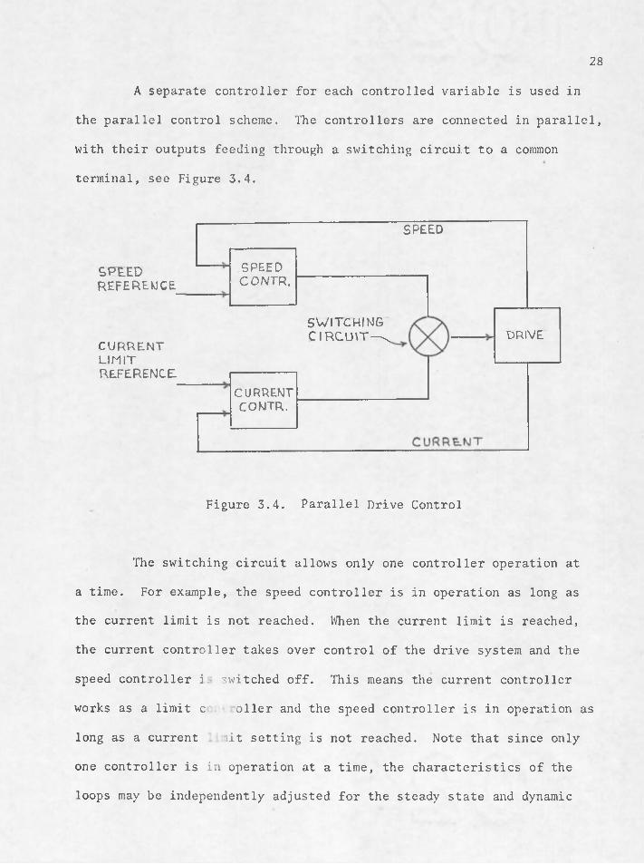
A separate controller for each controlled variable is used in the parallel control scheme. The controllers are connected in parallel,
with their outputs feeding through a switching circuit to a common terminal, see Figure 3.4.
SPEED
SPE.EDREFERENCE
SWITCHING C I RCU\T —\
CURRENTLIM ITREFERENCE
DRIVE
CURRENTCONTR.
SPEEDCONTR,
Figure 3.4. Parallel Drive Control
The switching circuit allows only one controller operation at a time. For example, the speed controller is in operation as long as the current limit is not reached. When the current limit is reached,
the current controller takes over control of the drive system and the
speed controller i. switched off. This means the current controller
works as a limit c oiler and the speed controller is in operation as
long as a current l i t setting is not reached. Note that since only one controller is i n operation at a time, the characteristics of the loops may be independently adjusted for the steady state and dynamic

29
responses desired. Adjustment of the controllers influences only the switch-over point.
Figure 3.5. Consider the diodes as ideal circuit elements with no forward voltage drop, hence the voltage V will always equal the larger of the two voltages and V^. The diode network is connected to the operational amplifier controllers as shown in Figure 3.6. The gain potentiometers IP and 2P are connected to the output of the switching circuit, not the amplifiers, thus allowing for proper switching of the parallel control, since the capacitors of the controller will now follow
the output to insure a smooth transition between the two controllers. With zero speed reference, diode ID is conducting and the output V of
the controller stays at zero. The output of amplifier 2 tends toward a negative value (due to the positive current reference input), reverse
biasing diode 2D which opens the feedback loop around the current
controller. The high open loop gain of amplifier 2 forces its output to the negative limit.
The switching circuit consists of the diode network shown in
? - 2 4 V
V
Figure 3.5. Switching Circuit

-24V
SPEEDFEEDBACKH O -----
+ 2 4 V IDSPEEDCONTROLLER
SPEEDREFERENCE
/ 7 7 T 7/ 7 7T7
CURRENTLIMITREFERENCE
(+>2D
CURRENTCONTROLLERZ77
CURRENT FEEDBACK g
Z7777
t i o v
Figure 3.6. Operational Amplifier Circuit for Control of Speed with Current Reference Limit wo
31
Should the speed reference input be increased to a value which would cause excessive armature current, the sum of the input currents
to the current controller would become negative., forcing its output to
switch to a positive limit. During the transient diode 2D becomes conductive, closing the feedback of amplifier 2 to the voltage existing at terminal V. Since diode ID starts blocking, opening the feedback loop of amplifier 1, the current controller takes over and the speed controller is switched off. As the speed approaches that called for by
the reference input, armature current falls below the current limit reference setting, and the speed controller comes out of its negative limit and regains control, switching off the current controller.
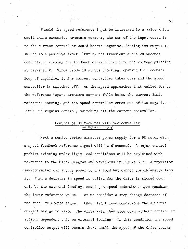
Control of DC Machines with Semiconverter as Power Supply
Next a semiconverter armature power supply for a DC motor with a speed feedback reference signal will be discussed. A major control
problem existing under light load conditions will be explained withreference to the block diagram and waveforms in Figure 3.7. A thyristor
semiconverter can supply power to the load but cannot absorb energy from
it. When a decrease in speed is called for the drive is slowed down only by the external loading, causing a speed undershoot upon reaching
the lower reference value. Let us consider a step change decrease of
the speed reference signal. Under light load conditions the armature current may go to zero. The drive will then slow down without controlleraction, dependent only on external loading. In this condition the speedcontroller output will remain there until the speed of the drive coasts

32
GATIH& MOD.SPEED
CONTROLLER TACKMOTORREFERENCE'
REFERENCE
SPEED
SPEEDCONTROLLEROUTPUT
T IM E
Figure 3.7. Machine Control with Semiconverter Power Supply
. ' ■ • . 33
below the new reference value prior to integrating up again. The time required for the output of the controller to reach the new reference
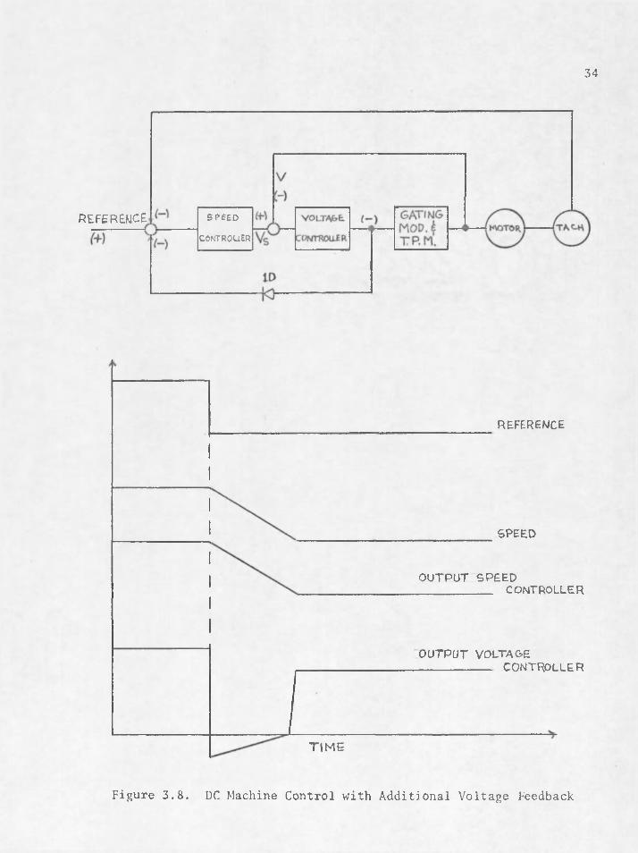
level causes an undershoot of the actual speed of the drive. This problem may be reduced substantially by additional feedback loops as
shown in Figure 3.8.The feedback voltage (V) of the voltage loop is proportional to
the output of the semiconverter during the normal operational and proportional to the motor CEMF at zero armature current when thyristors and diodes are non-conducting. Under normal operating conditions, the
high voltage gain of the voltage controller forces the feedback voltage
V to closely match the output of the speed controller .When the drive is slowed a small difference develops between V
and Vg which quickly forces the output of the voltage controller to reverse polarity, forward biasing diode ID. This closes a new control loop in which the voltage V can be considered the reference and the
voltage Vs the controlled variable. The output of the speed controller
will now closely follow the decrease in voltage V (due to the high gain of the voltage controller), which assures the speed controller of having the correct output when the new speed reference is reached by the drive.
The only time delay existing with this system is that of the time response of the voltage controller (which causes negligible speed undershoot) .
34
REFERENCEco ntro ller
S PEED
REFERENCE
SPEED
OUTPUT SPEEDCONTROLLER
OUTPUT VOLTAGECONTROLLER
TIME
Figure 3.8. DC Machine Control with Additional Voltage Feedback
CHAPTER 4
THE ELECTRICAL HARDWARE FOR MAGMA'S CASTING ROD PLANT SPEED REGULATING CONTROL SYSTEM
Cage Assembly
The cage assembly mounted within a motor control unit is for housing all the basic regulator cards (voltage, current, and speed cards). The assembly may hold combinations of four plug-in type printed
circuit boards used to provide the basic regulating functions. The four
cards are. listed below:
1. Gate pulse generator card.2. Current controller and gate pulse suppression card.3. Voltage controller card.
4. Speed controller card.The operation of the cards will be described in the following sections.
The cage assembly provides, in addition to the regulating cards, card interconnections, zener regulators and filters, pulse transformers, resistor board, and gate control transformer. The interconnections
consist of terminal blocks and wiring harness for A-C power connections
and control inputs and outputs to the regulating cards. Connecting the
gate pulse generation board and gate control transformer are diodes
comprising two rectifier circuits. The output voltage from these diode
rectifiers, 75 volts, is supplied to the zener regulators and filters

36
in the cage assembly to generate the +_ 24 volts for the controller modules, as shown in Figure 4.1.
Gate pulses are coupled from the gate pulse generator to the
thyristors in the semiconverter by three isolation pulse transformers as shown in Figure 4.2. Resistors mounted on a pegboard limit peak
power supplied to the thyristor gates and also complete a differential
voltage feedback loop. A gate control transformer mounted in the cage assembly provides proper phasing for the generation of gate pulses.
TPM Semiconverter
In Chapter 2 we discussed the operation of a three-phase semiconductor bridge circuit. In this section we will consider the
electrical operation of the Thyristor Power Module (TPM) in more depth.
In Figure 4.3 is shown a simplified schematic of the TPM. The
power transformer is shown in a wye-delta connection and provides isola
tion, adjusts line voltage to proper levels, and introduces inductance to limit rates of current during commutation. Phase-controlled gate pulses to fire the thyristors are provided by the gate pulse generator
described later. The DC output of the semiconverter is shown connected
to a motor armature load. A transfer equation relating the average output voltage to the firing angle a is shown in Appendix A [Kusko, 1969].
The voltage applied to the armature is controlled by the thyrsistors
Thyl, Thy2, Thy3. The diodes Dl, D2, D3 provide a current return path to most negative line terminal. The difference betwen voltage appliedby the bridge V to the motor and the armature voltage V is absorbedm a
G ATE PULSE RC. BCARD
CAGE ASS'Y
-24-PSM
GATE CONTROL TRANSFORMER SECONDARY
PSC
Figure 4.1. Zener Regulators and Filters
ui'vl

THYRISTOR p o w e r m o d u l e
r ______ Q_
L _ t-0_
it n !
ill______TPJ
RESISTORBOARD
8
T IVOLTA6E I
ICOMTROLLERj
;ind"i
GATE ) || P U L S E I II GENERATOR,
I S O L A T I O Nt r a n s f o r m e r ^
Figure 4.2. Isolation Transformer, Voltage Feedback Loop, and Gate Pulse Generation Card for a Thyristor Power Module

39
1-------I GATE 1 PULSE I GEN,I_______
r n
n
KJ
THY 1 THY 2 THY 3
D1 D2 D3x z
RC LINE FUSELS
CZEHp^-D C OUTPUT
„ FUSE
r C U R R E N T ^ L IM IT IN G
FUSES
A C LINE
W Y E -D E L T AT R A N S F O R M E R
Figure 4.3. Thyristor Power Module Scmiconverter

40
by the armature inductance and resistance. The free-wheeling diode acts at the end of a conduction period when the armature voltage attempts to reverse as the inductance discharges its energy. Included with a typical thyristor power module is an RC line filter connected
across each incoming line to limit incoming transient voltages, and
also output filters to provide a network to limit ringing associated with normal commutation. Current limiting fuses are provided in each line to protect the semiconductors during fault conditions, and a DC
output line fuse protects the motor against excessive currents or against failure by shorting of the free-wheeling diode 7D. Also provided is a thermal protection switch (not shown) embedded in a heat
sink to detect high temperatures in case of fan loss and turn off the TPM. -
Transductor; - . . '
The basic transductor used in the drive system described in
this paper provides isolation of positive and negative voltages propor
tional to the DC current monitored and provides thermal overload protection for the motor. A typical transfer curve relating output voltage to primary ampere turns is shown in Figure 4.4, The transductor is designed to provide feedback signals for current limit and gate pulse
suppression. A sensing circuit is shown in Figure 4.5.
VOLTS A
10-
0 11205G0AMPERE - T U R N S
Figure 4.4. Calibration Curve of Typical DC Current Transformer
42i n| S * 475/J476GO/ S^£09C 930HI3
/ Xcx— II
A/r
f ^ H r 1\2X5^ —__ S* *75# 475Go/
Figure 4.5. DC Current Sensing Circuit. (Courtesy of Westinghouse Electric Corporation.)
Gate Pulse Generator Card
The gate pulse generator card is one of four cards comprising the basic armature regulator for a DC motor control drive system. Each gate pulse generator card may be divided into four sections, a power supply section and three gate pulse circuit generator sections.
The gate control transformer, mounted in the rear of the cage
assembly, provides six-phase line to neutral voltages for the printed
circuit board. These voltages are rectified by two star rectifiers producing an unregulated +_ 75 volts DC. From the basic + 75 V^, a zener regulator provides +_ 24 volts for the controller module along with filter networks explained earlier. The + 75 volts feeding the
current control card is reduced by a voltage divider to + 40 volts and
43
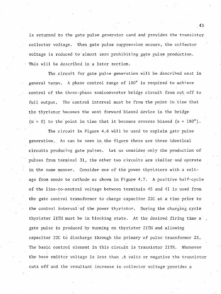
is returned to the gate pulse generator card and provides the transistor collector voltage. When gate pulse suppression occurs, the collector voltage is reduced to almost zero prohibiting gate pulse production.
This will be described in a later section.The circuit for gate pulse generation will be described next in
general terms. A phase control range of 180° is required to achieve control of the three-phase semiconverter bridge circuit from cut off to full output. The control interval must be from the point in time that
the thyristor becomes the most forward biased device in the bridge (a - 0) to the point in time that it becomes reverse biased (a = 180°).
The circuit in Figure 4.6 will be used to explain gate pulse
generation. As can be seen in the figure there are three identical circuits producing gate pulses. Let us consider only the production of pulses from terminal 31, the other two circuits are similar and operate in the same manner. Consider one of the power thyristors with a volt
age from anode to cathode as shown in Figure 4.7. A positive half-cycle of the line-to-neutral voltage between terminals 45 and 41 is used from
the gate control transformer to charge capacitor 22C at a time prior to
the control interval of the power thyristor. During the charging cycle
thyristor 21TH must be in blocking state. At the desired firing time a . gate pulse is produced by turning on thyristor 21TH and allowing capacitor 22C to discharge through the primary of pulse transformer 2X. The basic control element in this circuit is transistor 21TR. Whenever the base emitter voltage is less than .6 volts or negative the transistor
cuts off and the resultant increase in collector voltage provides a

44* /Si*y*OlCO/ - f O v . X /J i ty * a /C o f - SO*/t
/SO---------------- P% 3-
i n s
* 6 .0 /AT S.SSA’— c a—t-cria-Y_?<rs>
TP2k 1 ( J--OS/JO'Ws/w' y_ >
?3<r.
------%^r/so------ 9SD—?*/
n.pz/r <e4ur— aa— •-as—ios*
A
fW«96/T~eO.fSATr-y*3-
B /A S■5 I a/X«M O T E . - M L C t S t S T O S i . k R L C H W 1 1 C E P T W H E R E O T H E R W IS E J J O T E O© - T E S .T P I N o - E X T E R N A .L ( .T E R U I P T .)
Figure 4.6. Gate Pulse Generator Circuit. (Courtesy of Westinghouse Electric Corporation.)
45
A-K
22C
Figure 4.7. Voltage Waveforms of Thyristor, Capacitor, Transistor Input, and Trigger Pulses

46
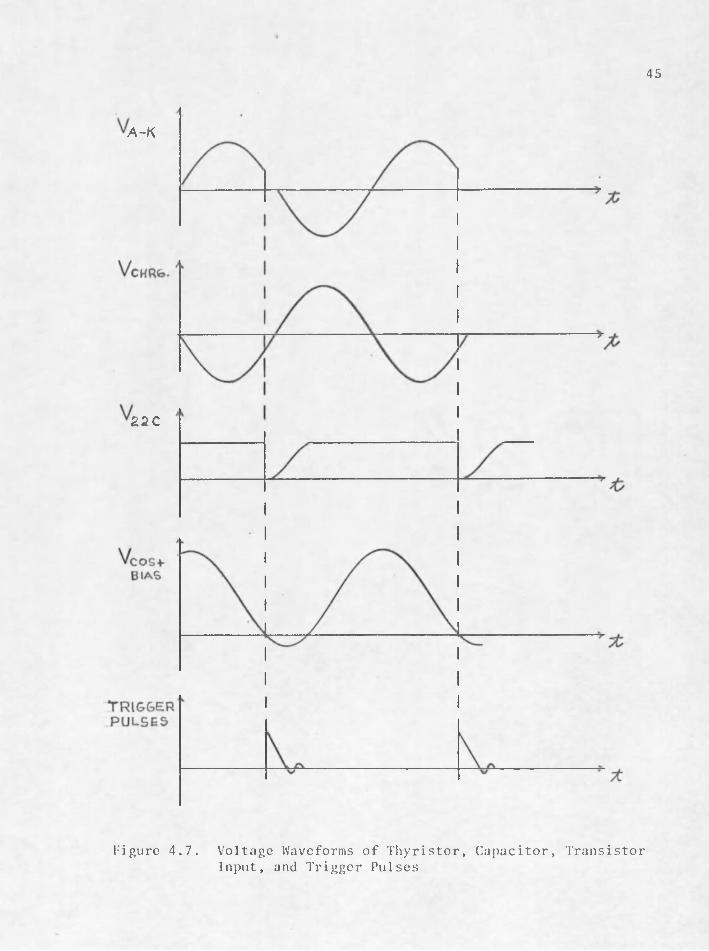
positive gate to 21TH, releasing a gate pulse as mentioned earlier.When the base-emitter voltage is greater than .6 volts the transistor
is turned on and the collector emitter voltage is .2 volts. The control of the base-emitter voltage or the point in time at which cut off occurs is determined by the bias voltage, the cosine voltage obtained from the filter consisting of 29R, 24C, and 20R, and the input voltage. As both the cosine voltage and bias are a fixed amplitude, phase control is
essentially a function of the input controller. A typical transfer
curve relating the voltage to the firing angle is shown in Figure 4.8.
Current Controller and Gate Pulse Suppression
The current controller and gate pulse suppression card is one of four printed circuit cards comprising the basic armature regulator. Figure 4.9 refers to the current controller and gate pulse suppression
card for the following discussion. The TOA 4X is an operational ampli
fier consisting of three-stage amplification. The first stage is a difference amplifier, the second stage an inverting amplifier, and the
third stage is an emitter follower circuit for the required current gain and low output impedance. Input signals to point B1 are inverted by the
OUT terminal point, with the amplifier having an open-loop gain of
approximately 2000.
Feedback components associated with the TOA 4X are designed to commit its use as a current controller. The diode network (2D,3D,4D,5D)
connecting the OUT terminal to B1 prevents the amplifier from saturating and limits its output voltage from +1 to -10.5 volts. Diode 7D is the
switching diode for the current controller, while resistor 18R provides
FIRINGANGLEo<
180 —
6 0 -
1 4 0 -
20 -
OO -
80 -
b O —
4 0 -
2 0 -
-106OVOLTS-IN
Figure 4.8. Transfer Curve of V. vs. ain

48srr/f osr scr* /rrprs fas+f-'A/Arro jciyLtp>.--je>£- usro
mc.A 0 3 6 0 / nafr/far rrsyaarrcx* hlOy/JL/3aCcAO2G0Z t3 aG A 0 2 G 03
srsro jprsoe/jrop \iOr/£ rv: jvt<vctna^ra/r rYsye/}/'cva , 6/* /&r /vr "as.ss
ss(~t*)
3* & tmr
70
3C
G*Te />utse
37C
B6X
333/f?) fa) r-»)fiS O T l t A L L r O K i > /> /? £ <3 S *V £X<1 L P T * / * - / £ * ? £ . O T - A / £ / 7 t V / S £ A J O T t Oz /'ovf m o h c k OA/AJ ; *i j /s ccxja/ac. re & ro re/?** 2 6 aocofjK/tcre 7ZJ7" pmO* £at£/?mal (t£Pah or.)
Figure 4.9. Current Controller and Gate Pulse Suppression.(Courtesy of Westinghouse Electric Corporation.)

49
the reverse bias for all switching diodes in parallel regulators. When used in voltage or speed regulators the current controller provides a current limit function adjustable by pot 6P. For current regulation, a signal proportional to the armature current is brought in to termal 55 and compared with the reference signal. The indicated jumpers allow the printed circuit board to be checked for various performance parameters or to disconnect the current controller to allow parallel
regulator loops to be checked independently.The gate pulse suppression portion of the circuit consists of
all the components below terminal 39 (found on the righthand side of the figure). Appearing at terminal 41 is a +75 volts from the bridge rectifier of the gate pulse generator card. Normally thyristor 1TH is
in the blocking state, and by voltage divider action the +40 volts is
returned from terminal 43 to the gate pulse generator card, providing the transistor collector voltage. Feeding terminal 37 is a signal (from
the transductor described earlier) proportional to the armature current,
and by adjusting pot IP the gating level of the thyristor is set to a predetermined fault current level (approximately 25% greater than the
drive current limit setting). Once gated, the voltage at terminal 43 is
the forward voltage drop of thyristor 1TH, which prevents further gate pulses by the gate pulse generator card. By inhibiting gate pulse pro
duction the failure of devices may be limited to the thyristor in conduction, the bridge diodes conducting when the fault occurs and associated line fuses. Also shown in the circuit diagram are three relays. ICR resets the integrating capacitor, capacitor 4C, by provid
ing a quick discharge path when the drive is turned off. Relay coil 86Y

50
is provided to sequence the drive off in the event of gate pulse
suppression. Relay coil 86X is provided to reset thyristor 1TH after gate pulse suppression. As 1TH is forward biased, once gated on it continues to conduct until 86X is de-energized. Closure of 86X contact shunts current from the thyristor until it reaches a current less than holding current which causes the thyristor to revert to its blocking state.
Voltage Controller
The voltage controller card is one of four printed circuit boards comprising the basic armature regulator. The differential oper
ational amplifier and associated feedback components comprise the basic voltage regulator as seen in Figure 4.10.
Considering the differential amplifier, a small voltage applied -between points B1 and B2 will be amplified through two stages. These
two stages provide a DC differential voltage gain of approximately 4000.
For this amplifier a positive differential error signal (B1 positive
with respect to B2) will yield a positive output from E01 and an equal
and opposite negative output from E02.
The feedback components associated with the difference amplifier provide a controller function of a time delay amplifier. The voltage
output of the amplifier is limited by the transistors and diodes 10TR, 11TR, 10D, and 11D respectively to approximately +_ 10.5 volts as set by
the voltage divider network of 31R and 37R. The voltage loop is closed through the resistors mounted in the basic cage assembly which connects

51s r y i e O S f /r fM S fz /p f /A /z fr y o iZi/AlPZ'yPS" Z&ZZP
/ i Z k A C i O O ! S'/Atr/z zzy>z" I 'O / r ^ s s z >/iP C n A O B C .-O a A * y z r /- /^ p /j'S y a p T y p s f <v/ 3 P C ,A 0 3 0 0 3 s p y -’/? /p y & o 'z /p r& s ’ - s j p , /o ? y y/3 e C > A O 3 0 0 d S<rP. SOZ] 6 P . S P /o r Z o r n s '
(*>33
Yon/\c,e L/Mtr Q*.V’CfO
JAJAf
Vt’p.2)
55(T . f t ! )
TO OK- I
AJOTC. /. »(.L /*/?« 0.6 tV© 0I£>CO*jkj£C.T O £XTe.f?KIAL. ( T£#MI PT.')© r^sr P iki
Figure 4.10. Voltage Controller. (Courtesy of Westinghouse Electric Corporation.)
52
the output terminals of the thyristor power module with the input terminals 31 and 33 of the voltage controller card. Control input signals are fed into base 1 of the amplifier. For the speed regulator under discussion in this paper IR compensation is not used, hence items 34R, 15C, IOC, 6P and 5P are eliminated. The jumpers used are 1J, 2J,
5J, and 6J. Because in a speed controller armature regulator system the voltage controller card is not used in a parallel configuration, diode 12D is also eliminated. Inside DA-1 are two small.squares labeled DIF7P and CM8P which represent differential balance and common-made
balance adjustments for the DC amplifier.
Speed Controller and Ramp-Function Generator
The speed controller and ramp-function generator card is one of
four printed circuit boards comprising the basic armature regulator.The ramp-function generator option which produces a linear change in
output voltage from an abrupt change in input voltage, was not used in
the individual control system units at Magma and will not be described any further here.
The speed controller consists of a DC PIOIA amplifier and
associated feedback components as seen in Figure 4.11. The PIOIA amplifier consists of three-stage amplification, with the first two stages being differential type and the third stage consisting of an
inverter and two direct-couple transistors providing current gain. The
amplifier has an open-loop voltage gain of approximately 20,000, and all plus voltage inputs to B1 yield negative output voltages. Components 2D, 3D and 6D, 7D prevent the amplifier from saturating, limiting

(fACH) O —
I ^
&%>'
ic pxla r I-K— | srcsc?COACT/?Ol-L£f?
.0*7A?ZZ7•-P/OM
rWzs?
ZVJA/Z’ /rusSCT/OSV CPACPJPATOA?PAMP K|S
T/n£ u p
P-OUTxepoAOJ.
'T7 s.T-ALL *£SISTO#S A*/r '/m U <MU£S5 or*f#U/S£ &P£C/f/£D
Figure 4.11. Speed Controller and Ramp Function Generator.(Courtesy of Westinghouse Electric Corporation.)
54
the output to +1 volt and -10.5 volts. Diode 5D prevents reverse voltages from being developed across capacitor 9C, and capacitor 10C limits
the output response for step inputs to the speed controller. Diode 4D is the logic switching diode, with the required reverse biasing provided through the 18R resistor in the current controller card. Removeable board jumpter 4J disconnects the speed controller, allowing for performance checks of other independent controller loops. Terminal 35 is connected to the output of the voltage controller card and closes a control loop which prevents undershoot for speed control encountered while decelerating under light load conditions.

CHAPTER 5
' CONCLUSIONS
The discussion presented in this work has introduced the static
conversion equipment used in a thyristor power system by Magma Copper Company for a speed-regulated DC motor control drive. In the past the DC motor was powered by the DC generator. Within recent years however, the development of operational amplifiers, thyristor amplifiers, and
thyristor power supplies has been used to eliminate the generator in
many applications.There are several essential advantages of the thyristor power
system. One such advantage is the lower maintenance requirements. Al
though the DC generator is dependable, its bearings require maintenance,
the commutator requires careful handling, brushes need periodic replace
ment, and armature insulation breakdowns must be avoided. Other advan
tages include a 3 or 4 percent increased efficiency at rated load, smaller size, lower weight, lower installation cost, and faster time
response. Some disadvantages of the thyristor power supply are lower
power-factor, power-factor correction ability is lost, and no regenera
tion capability.
It is hoped that the interested reader will find the basic
principles and circuits presented here a guide to better understanding of modern industrial control system.
55
APPENDIX A
A DERIVATION FOR THE AVERAGE LOAD VOLTAGE VS. FIRING ANGLE FOR A THREE-PHASE THYRISTOR SUPPLY
A transfer equation and curve is found by relating the average
load voltage Vg of a three phase thyristor power supply to the firingangle a by integrating the output voltage waveshape with respect to a.
Let the supply voltage be expressed by:
v = /2 V sin wt (1)s s
where V^ is the R.M.S. line voltage. The average supply voltage is
Vs(AVE) = Vs d(wt) ' (2)
Sub equation (1) into (2) yields
Vs(AVE) = Vs Sin wt d(Wt) •
For a three-phase semiconverter circuit where the thyristors
are triggered at angle a, the mean supply voltage over a complete cycle is:
3 /2 V 7Trs(AVE) = 2tt / s i n s t d ( " t ) •a
56

Evaluating the integral:
Vs(AVE)3 /2 V(
27T -cos wtTT
aS y/2
277 1 + cosa
3 V/2 TT
1 + cosa = .675 Vs [1 + cosa]
The transfer curve relating the average load voltage to the
firing angle may be seen in Figure A-l.

58
S O 150IOOFIRING ANGLE oC
Figure A-l. Average Load Voltage vs. Firing Angle

REFERENCES
Fitzgerald, A. E., Charles Kingsley, Jr., and Alexander Kusko. Electric Machinery. McGraw-Hill, 1971.
Kusko, Alexander. Solid-State DC Motor Drives. M.I.T. Press, 1969.Mazda, F. F. Thyristor Control. London, Newnes-Buttervvorths, 1973.
Morris, Noel. Advanced Industrial Electronics. McGraw-Hill, 1974.
Rose, M. J . Techniques of Thyristor Power Control, Vol. 1, PowerEngineering Using Thyristors, Technical Services, MuHard Ltd., 1970.
Westinghouse Electric Corporation. Industrial Systems Division Instruction Book, Buffalo, New York, April 1971.
59

*k
0 * > 6 7 b 0