electrical characterization of deposited …efug.imec.be/efug2006_volbert.pdfthis is convenient for...

1
The four-point probe unit has a 5 µm pitch. The cantilever is 25 µm long and has a thickness of 3 µm and a width of 5 µm. The spring constant is 5 N/m. The unit is connected to the electronic circuitry by suitable feed-through. As the touch down needs to be arranged along the deposition line, the sample is mounted horizontally so that images of the SEM column can be used. Touch down is realized by slowly moving downward with the MM3A while monitoring a DC voltage off-set, that drops upon touch down. An example of this procedure is shown in figure 5, using an ion beam induced Pt deposition of 25 x 1 x 1 µm. Given the spring constant and the overdrive of 1 µm, the actual contact force was around 5 µN. Introduction Electron and ion beam systems can be applied for the local deposition of material. This is realized by the local decomposition of organo-metallic precursor gas, released close to the surface of interest. The excellent control of the beam position and dwell time, allow the creation of well defined structures at the micro and nano scale. In application of these depositions for semi-conductor and nano technology it is important to understand the electrical, optical, mechanical, magnetic or chemical properties of such a deposition. Especially metallic depositions are often used for the direct creation of a very local conductivity path and hence the local resistance of a structure is an important parameter. For this reason the electrical characterization of metallic deposits of thin metal lines ( .m) or of thin films (/sq) is necessary. The standard characterization method For the determination of the specific resistivity of a metal line, use is made of the four point probe method. In this method a wire or a small structure is contacted at four locations (pin 1, 2, 3, 4). Pin 1 A L w t Pin 2 Pin 3 Pin 4 i i V Ion or electron beam deposited strip The measurement method then includes a forced current i through the outer pins 1 and 4 and a measurement of the voltage drop over pin 2 and 3, using a very high Ohmic measurement device, so that the current flowing through pin 2 and 3 is nearly zero. In that case the individual, additional contact resistance does not play a role as it cancels out of the equation. To study the behavior of the structure an i/V curve is generated, typically in the µ A to the mA range. If the graph shows a straight line, the structure behaves as an Ohmic resistor. If we assume the resistance of a structure to be R then the following applies: R = ρ. L / A with L = the length of the structure (m); A = the area (width x thickness) of the cross section (m ) ρ = the specific resistivity (.m or the practical unit µ.cm) As the structures created by the ion beam or by the electron beam are very small, the way of contacting them is not straightforward. One of the ways to do the measurements is to create a deposition of a metal strip over the area of a pre-patterned wafer, where the strip connects to all four, large probe pads of the pre-defined pattern. In this way large pads (up to mm) become available for the probing. An example of such a dedicated structure is shown in figure 1 (overview) and the details of a deposited Au structure are shown in figure 2 (tilted image). In the description above and referring to figure 1, pin 1 and 4 are the pads in the upper left and right corner, whereas pin 2 and 3 are the pads on the lower left and lower right corner. By applying the probe measurements to the four pads the resistance between connection 2 and 3 is known and measuring the distance between the probe pads 2 and 3 (L) as well as the cross sectional area of the deposit (width and thickness), the specific resistivity can be determined. Although the method gives good results, it requires the use a special test wafer structure and the measurement cannot be done on an arbitrary substrate of interest, such as a polymer, a glass base, an optical structure or any bio-active material. In addition, as can be seen from the pictures above, the pre-patterned wafer is not quite perfect and the deposit includes a four-fold step-coverage. Also the width and thickness of the metal deposition have to be determined from the tilted image or from a FIB created cross-section. Depending on the gas deposition conditions, the step coverage's left and right may be different. Finally, it is necessary to prepare the pre-patterned wafer so that Ohmic contact can be made between the pad and the deposit. So any oxide barrier must be removed completely before depositing. Figure 1 (left) shows an example of a structure suited for the measurement. Figure 2 (right) shows the details of a single strip (Au deposition, tilted image) that connects all 4 probe pads. Figure 3 (left): Quanta3D stage mounting of the MM3A manipulator and the four-point probe unit for contacting a vertically mounted sample. In a vertical position the distance between probe and sample can be measured using the SEM image. This is convenient for sheet film measurements, as the lateral positioning is not critical. Fig 4 (right): detail of the probe tips. A new approach A more direct way to measure the specific resistivity is to apply in-situ probing on a metal deposition strip, which is isolated on a flat structure. In that case there is no step coverage and the strip usually is better defined (area of the cross-section). As the only requirement is the use of a non-conducting flat background, the strip can be deposited on any substrate of interest, such as a polymer thin film. In a practical approach this method has been tested using an FEI Quanta3D and an in-situ Capres four-point probe unit mounted on a Kleindiek MM3A micro-manipulator. The Capres system includes a more sophisticated electronic measurement system based on a low frequency AC current source and a resulting voltage that is measured using a lock-in amplifier and suitable output filtering. In this way it is possible to get good readings in the very low voltage range (low current, low resistance) with good noise suppression and elimination of DC artifacts. The current frequency range is up to 650 Hz, but the resistance measurement result is, of course if ohmic, independent of the applied frequency. The choice of frequency is optimized for the best accuracy of the measurement. The experimental set-up is shown in figure 3 and the probe unit detail in figure 4. Fig 5 (left): Image of the ion beam created Pt strip and the 4 point probe above it, prior to touch down, pins are grounded. Fig 6 (right): Just before touch down a stroboscopic voltage contrast with large DC off-set is visible at relative fast scan rate. At the moment of touch down this contrast disappears. Fig 7 (left): Image during the measurement. The probe unit now is in touch down position and the determined resistance is 50.8 . Fig 8 (right): Probe removed from the strip, after the measurement. Pins are grounded. The strip shows very small indents due to the touch down. Result The measured value of 50.8 allows the calculation of ρ using and area of 10 µm and a length of 5.10 µm: ρ=1.10 .m or 10 µΩ.m. This compares favorably with values reported in literature of between 10 –20 µΩ.m. The actual measurement is done in typically one second per point on the i/V curve. In a full curve the linear behavior of the resistor can be checked as well, and any Schottky behavior would be visible form the curvature in the graph. In the case mentioned here, the contact is Ohmic. Conclusion The in-situ measurement method using the four-point probe unit provides direct measurement of the specific resistivity of the deposition, created by the electron beam or by the ion beam. It can be applied to "stand-alone" structures on any isolating substrate. The in-situ measurement can be used to study the deposition process parameters (chemical environment, ion / electron beam settings, substrate type, temperature, patterning parameters etc) without the requirement for dedicated pre-patterned wafers. Discussion The control of any residual damage is strongly related to the force of the contact and in practice to the speed of approaching and hence the time spent on contacting. The applied speed in the example above is an average one and in case more time is spent, the resulting indents will even be less. In the example here the indents are visible, but the damage does not change the structure notably and has no influence on the measurement result. The measurement has also been repeated at different positions on the strip: they all had the same value of 50.8 , indicating that the result is representative for the material of the strip. ELECTRICAL CHARACTERIZATION OF DEPOSITED STRUCTURES BY 4- POINT –PROBING Stephan Kleindiek, Hans Mulders, Bernd Volbert Kleindiek Nanotechnik GmbH , Aspenhaustrasse 25, 72770 Reutlingen, Germany FEI Company, Achtseweg Noord 5, 5600 KA Eindhoven, Nederland Namitec, Amerlaan 55, 5626 BR Eindhoven, Nederland. Correspondence: [email protected] -12 2 -6 -5

Upload: hatuyen

Post on 28-Jun-2019

213 views

Category:

Documents


0 download

TRANSCRIPT

The four-point probe unit has a 5 µm pitch. The cantilever is 25 µm long and has a thickness of 3 µmand a width of 5 µm. The spring constant is 5 N/m. The unit is connected to the electronic circuitry bysuitable feed-through. As the touch down needs to be arranged along the deposition line, the sampleis mounted horizontally so that images of the SEM column can be used.

Touch down is realized by slowly moving downward with the MM3A while monitoring a DC voltageoff-set, that drops upon touch down. An example of this procedure is shown in figure 5, using an ionbeam induced Pt deposition of 25 x 1 x 1 µm. Given the spring constant and the overdrive of 1 µm,the actual contact force was around 5 µN.

Introduction

Electron and ion beam systems can be applied for the local deposition of material. This is realized bythe local decomposition of organo-metallic precursor gas, released close to the surface of interest.The excellent control of the beam position and dwell time, allow the creation of well defined structuresat the micro and nano scale. In application of these depositions for semi-conductor and nano technologyit is important to understand the electrical, optical, mechanical, magnetic or chemical properties of sucha deposition. Especially metallic depositions are often used for the direct creation of a very localconductivity path and hence the local resistance of a structure is an important parameter. For this reasonthe electrical characterization of metallic deposits of thin metal lines (Ω.m) or of thin films (Ω/sq) isnecessary.

The standard characterization method

For the determination of the specific resistivity of a metal line, use is made of the four point probe method.In this method a wire or a small structure is contacted at four locations (pin 1, 2, 3, 4).

Pin 1

A

L

wt

Pin 2

Pin 3

Pin 4

i

i

V

Ion or electron beam deposited strip

The measurement method then includes a forced current i through the outer pins 1 and 4 and ameasurement of the voltage drop over pin 2 and 3, using a very high Ohmic measurement device, sothat the current flowing through pin 2 and 3 is nearly zero. In that case the individual, additional contactresistance does not play a role as it cancels out of the equation. To study the behavior of the structurean i/V curve is generated, typically in the µ A to the mA range. If the graph shows a straight line, thestructure behaves as an Ohmic resistor. If we assume the resistance of a structure to be R then thefollowing applies:

R = ρ. L / A

with L = the length of the structure (m); A = the area (width x thickness) of the cross section (m ) ρ = the specific resistivity (Ω.m or the practical unit µΩ .cm)

As the structures created by the ion beam or by the electron beam are very small, the way of contactingthem is not straightforward. One of the ways to do the measurements is to create a deposition of a metalstrip over the area of a pre-patterned wafer, where the strip connects to all four, large probe pads of thepre-defined pattern. In this way large pads (up to mm) become available for the probing. An exampleof such a dedicated structure is shown in figure 1 (overview) and the details of a deposited Au structureare shown in figure 2 (tilted image). In the description above and referring to figure 1, pin 1 and 4 arethe pads in the upper left and right corner, whereas pin 2 and 3 are the pads on the lower left and lowerright corner.

By applying the probe measurements to the four pads the resistance between connection 2 and 3is known and measuring the distance between the probe pads 2 and 3 (L) as well as the cross sectionalarea of the deposit (width and thickness), the specific resistivity can be determined. Although the methodgives good results, it requires the use a special test wafer structure and the measurement cannot bedone on an arbitrary substrate of interest, such as a polymer, a glass base, an optical structure or anybio-active material. In addition, as can be seen from the pictures above, the pre-patterned wafer is notquite perfect and the deposit includes a four-fold step-coverage. Also the width and thickness of the metaldeposition have to be determined from the tilted image or from a FIB created cross-section. Depending onthe gas deposition conditions, the step coverage's left and right may be different. Finally, it is necessaryto prepare the pre-patterned wafer so that Ohmic contact can be made between the pad and the deposit.So any oxide barrier must be removed completely before depositing.

Figure 1 (left) shows an example of a structure suited for the measurement. Figure 2 (right)shows the details of a single strip (Au deposition, tilted image) that connects all 4 probe pads.

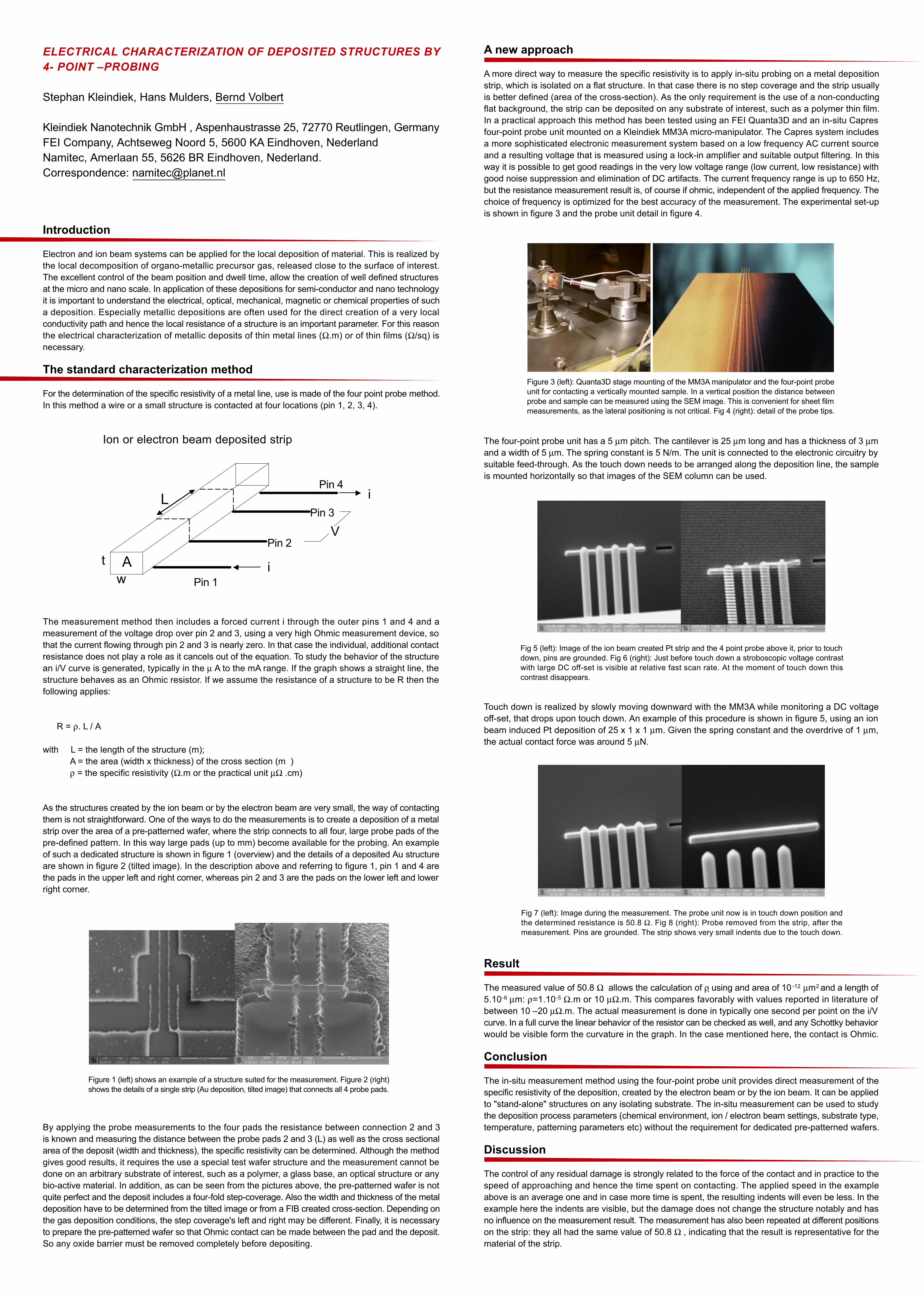
Figure 3 (left): Quanta3D stage mounting of the MM3A manipulator and the four-point probeunit for contacting a vertically mounted sample. In a vertical position the distance betweenprobe and sample can be measured using the SEM image. This is convenient for sheet filmmeasurements, as the lateral positioning is not critical. Fig 4 (right): detail of the probe tips.

A new approach A more direct way to measure the specific resistivity is to apply in-situ probing on a metal depositionstrip, which is isolated on a flat structure. In that case there is no step coverage and the strip usuallyis better defined (area of the cross-section). As the only requirement is the use of a non-conductingflat background, the strip can be deposited on any substrate of interest, such as a polymer thin film.In a practical approach this method has been tested using an FEI Quanta3D and an in-situ Capresfour-point probe unit mounted on a Kleindiek MM3A micro-manipulator. The Capres system includesa more sophisticated electronic measurement system based on a low frequency AC current sourceand a resulting voltage that is measured using a lock-in amplifier and suitable output filtering. In thisway it is possible to get good readings in the very low voltage range (low current, low resistance) withgood noise suppression and elimination of DC artifacts. The current frequency range is up to 650 Hz,but the resistance measurement result is, of course if ohmic, independent of the applied frequency. Thechoice of frequency is optimized for the best accuracy of the measurement. The experimental set-up is shown in figure 3 and the probe unit detail in figure 4.

Fig 5 (left): Image of the ion beam created Pt strip and the 4 point probe above it, prior to touchdown, pins are grounded. Fig 6 (right): Just before touch down a stroboscopic voltage contrastwith large DC off-set is visible at relative fast scan rate. At the moment of touch down thiscontrast disappears.

Fig 7 (left): Image during the measurement. The probe unit now is in touch down position andthe determined resistance is 50.8 Ω. Fig 8 (right): Probe removed from the strip, after themeasurement. Pins are grounded. The strip shows very small indents due to the touch down.

Result

The measured value of 50.8 Ω allows the calculation of ρ using and area of 10 µm and a length of5.10 µm: ρ=1.10 Ω.m or 10 µΩ.m. This compares favorably with values reported in literature ofbetween 10 –20 µΩ.m. The actual measurement is done in typically one second per point on the i/Vcurve. In a full curve the linear behavior of the resistor can be checked as well, and any Schottky behaviorwould be visible form the curvature in the graph. In the case mentioned here, the contact is Ohmic.

Conclusion

The in-situ measurement method using the four-point probe unit provides direct measurement of thespecific resistivity of the deposition, created by the electron beam or by the ion beam. It can be appliedto "stand-alone" structures on any isolating substrate. The in-situ measurement can be used to studythe deposition process parameters (chemical environment, ion / electron beam settings, substrate type,temperature, patterning parameters etc) without the requirement for dedicated pre-patterned wafers. Discussion

The control of any residual damage is strongly related to the force of the contact and in practice to thespeed of approaching and hence the time spent on contacting. The applied speed in the exampleabove is an average one and in case more time is spent, the resulting indents will even be less. In theexample here the indents are visible, but the damage does not change the structure notably and hasno influence on the measurement result. The measurement has also been repeated at different positionson the strip: they all had the same value of 50.8 Ω , indicating that the result is representative for thematerial of the strip.

ELECTRICAL CHARACTERIZATION OF DEPOSITED STRUCTURES BY4- POINT –PROBING

Stephan Kleindiek, Hans Mulders, Bernd Volbert

Kleindiek Nanotechnik GmbH , Aspenhaustrasse 25, 72770 Reutlingen, GermanyFEI Company, Achtseweg Noord 5, 5600 KA Eindhoven, NederlandNamitec, Amerlaan 55, 5626 BR Eindhoven, Nederland. Correspondence: [email protected]

-12 2

-6 -5