electrical and computing engineering filereconfigurable antennas using mems . carla sofia dos reis...
TRANSCRIPT

Reconfigurable Antennas Using MEMS
Carla Sofia dos Reis Medeiros
Master’s Degree Dissertation in
Electrical and Computing Engineering
Jury President: Prof. António Castelo Branco Rodrigues, IST
Supervisor: Prof. Carlos António Cardoso Fernandes, IST
Co-supervisor: Prof. Jorge Rodrigues da Costa, ISCTE
Member: Prof. Custódio José de Oliveira Peixeiro, IST
October 2007


ACKNOWLEDGEMENTS
I would like to express my most sincere gratitude to Prof. Carlos Fernandes, my supervisor, and
to Prof. Jorge Costa, my co-supervisor, for the support, guidance and dedication through the
elaboration of this work.
To Mr. António Almeida for performing the measurements of the antennas and for the
suggestions and help during this work.
To Mr. Vasco Fred and Mr. Carlos Brito for the fabrication of the antennas and for the useful
recommendations.
To my colleagues at Instituto Superior Técnico and at Instituto de Telecomunicações for the
friendship, support and suggestions.
The work presented on this thesis was developed in the framework of R-META project
““Reconfigurable Low-profile Antennas Using Metamaterials” – POSC/EEA-CPS/61887/2004 – funded
by Fundação de Ciência e Tecnologia, FCT, under the POS_Conhecimeto program co-funded by
FEDER.
i


iii
ABSTRACT
This work investigates the feasibility of using a commercial numerical electromagnetic solver -
WIPL-D Microwave - to completely model reconfigurable patch antennas using packaged RF MEMS
switches. The proposed model takes into account not only the switch RF characteristic through its
scattering matrix, but also the influence of the MEMS encapsulation and DC actuation circuit on
antenna performance in terms of impedance and radiation pattern. To achieve this, a procedure is
proposed using WIPL-D Microwave to combine a 3D EM analysis of the antenna with a microwave
circuit analysis. The MEMS scattering matrix is de-embedded from measurements performed on a
dedicated test circuit and, for comparison purposes, the equivalent lumped element circuits are
calculated.
The selected antenna’s configurations for testing the procedure are based on a square patch
with one or two slots, the MEMS being used to either short or leave the slots open, enabling to switch
the operating frequencies while maintaining good input impedance match and stable radiation
characteristics, in the 2 to 3 GHz frequency band. This simple antenna’s structures enables to focus
on the modelling of commercial packaged MEMS and on the resulting accuracy of the antenna
simulation prediction, rather than focus on the antenna optimization.
The test antennas were designed and manufactured and the experimental results agree well
with simulations, thus validating the proposed modelling procedure: The results were published and
presented at two conferences and submitted to a Journal.
Keywords Reconfigurable patch antennas, Frequency agility, Packaged RF MEMS switches, Full wave
3D modelling.


v
RESUMO
Este trabalho tem como objectivo avaliar a viabilidade de se usar um simulador
electromagnético comercial (WIPL-D Microwave) para a modelação de antenas impressas
reconfiguráveis que incluam interruptores RF MEMS encapsulados. O modelo proposto permite a
análise do desempenho da antena em termos de impedância de entrada e características de
radiação. A simulação tem em consideração não só as características RF dos interruptores, através
da matriz de dispersão, como também a influência do encapsulamento metálico do MEMS e do
respectivo circuito de actuação DC. Com este intuito, propõe-se um procedimento que combina a
análise electromagnética 3D das antenas com a análise de circuitos de microondas utilizando o
WIPL-D Microwave. A matriz de dispersão dos MEMS é extraída dos resultados medidos num circuito
de teste, devidamente elaborado para esse efeito, e é calculado o modelo equivalente do interruptor.
As configurações de antenas seleccionadas para validação do modelo proposto baseiam-se
em antenas impressas quadradas incluindo uma ou duas fendas rectangulares, as quais podem ou
não ser curto-circuitadas pelo interruptor RF MEMS. Deste modo é possível comutar a frequência de
ressonância das antenas mantendo simultaneamente uma boa adaptação da impedância de entrada
assim como as características de radiação da antena, na banda de frequência dos 2 aos 3 GHz. A
estrutura simples das antenas permite manter a ênfase na modelação dos MEMS comercias e na
precisão da simulação, em vez de se focalizar na optimização da antena.
As antenas foram projectadas e fabricadas e os resultados experimentais estão concordantes
com as simulações, corroborando o modelo e o procedimento proposto. Os resultados foram
publicados e apresentados em duas conferências e submetidos para publicação em revista científica.
Palavras-Chave Antenas impressas reconfiguráveis, Comutação na frequência, Interruptores RF MEMS
encapsulados, Modelação Electromagnética 3D.


CONTENTS
Acknowledgements.......................................................................................................................i Abstract....................................................................................................................................... iii Resumo .......................................................................................................................................v Contents ....................................................................................................................................vii List of Figures .............................................................................................................................ix List of Tables ............................................................................................................................ xiii List of Abbreviations ..................................................................................................................xv Chapter 1 - Introduction.............................................................................................................. 1
1.1. Overview .......................................................................................................................... 1 1.2. State of the art.................................................................................................................. 4 1.3. RF MEMS Switches ......................................................................................................... 5 1.4. Thesis Organization ......................................................................................................... 7
Chapter 2 - RF MEMS switches Characterization...................................................................... 9 2.1. Objectives ........................................................................................................................ 9 2.2. WIPL-D EM and WIPL-D MW Overview........................................................................ 10 2.3. RF MEMS switch basic description................................................................................ 10 2.4. S-matrix De-embedding Procedure ............................................................................... 12 2.5. Experimental Issues....................................................................................................... 14 2.6. Influence of the Encapsulation....................................................................................... 21 2.7. Conclusions.................................................................................................................... 26
Chapter 3 – Reconfigurable Antennas Simulation models....................................................... 27 3.1. Objectives ...................................................................................................................... 27 3.2. MEMS Reconfigurable Patch antenna with one slot...................................................... 28 3.3. MEMS Reconfigurable Patch antenna with two slots .................................................... 32 3.4. Patch antenna with two slots using Ideal Switches ....................................................... 36 3.5. Conclusions.................................................................................................................... 38
Chapter 4 – Experimental Results............................................................................................ 39 4.1. Objectives ...................................................................................................................... 39 4.2. MEMS Reconfigurable Patch antenna with one slot...................................................... 40 4.3. MEMS Reconfigurable Patch antenna with two slots .................................................... 43 4.4. Patch antenna with two slots using Ideal Switches ....................................................... 47 4.5. Evaluation of tick substrate de-embedded S-Matrix ...................................................... 49
vii

viii
4.6. Gain and Radiation Efficiency........................................................................................ 51 4.7. Conclusions.................................................................................................................... 52
Chapter 5 – Conclusions and Future Work .............................................................................. 53 Annexes.................................................................................................................................... 57 ANNEX A Manufacturing process ....................................................................................... 59
A.1 Antenna mask ......................................................................................................... 59 A.2 Photolithographic process....................................................................................... 59 A.3 Fabrication process................................................................................................. 60
ANNEX B Antenna analysis and simulation ........................................................................ 61 B.1 Method of Moments (MoM)..................................................................................... 61 B.2 WIPL-D software ..................................................................................................... 62
ANNEX C Study of Patch Antenna Parameters .................................................................. 65 ANNEX D Radiation Efficiency measurements ................................................................... 70 References ............................................................................................................................... 79

LIST OF FIGURES
Figure 1.1 –Operating principle of RF-MEMS switches devices: (a) Resistive series switch; (b)
Capacitive shunt switch. .......................................................................................................................... 6 Figure 1.2 – Teravicta TT712-68CSP RF MEMS switch operating principle. ............................ 7 Figure 2.1 – Teravicta MEMS switch: (a) Front and back photo; (b) Pin description. .............. 11 Figure 2.2 – Teravicta TT712-68CSP RF MEMS switch characteristic curves provided by
manufacturer [2] for an input impedance of 50 Ω.................................................................................. 12 Figure 2.3 – Equivalent model of the measured test circuit which includes the device under
test (DUT). ............................................................................................................................................. 13 Figure 2.4 - Photo of manufactured test circuits: (a) 50 Ω microstrip reference line; (b) Test
circuit, before mounting the MEMS switch. ........................................................................................... 14 Figure 2.5 – Photo of manufactured prototype: (a) Test circuit with MEMS and 100 kΩ
resistors at the DC path; (b) Zoomed view of the MEMS switch and resistors; (c) Zoomed view of the
DC and RF lines that connect to the MEMS.......................................................................................... 14 Figure 2.6 – 50 Ω microstrip reference line: (a) Electromagnetic model; (b) Microwave circuit
model with connectors........................................................................................................................... 15 Figure 2.7 – Measured and simulated return loss of the 50 Ω reference line: (a) Magnitude; (b)
Phase..................................................................................................................................................... 16 Figure 2.8 -– Measured and simulated insertion loss of the 50 Ω reference line: (a) Magnitude;
(b) Phase. .............................................................................................................................................. 16 Figure 2.9 – Test circuit without MEMS: (a) Electromagnetic model; (b) Microwave model with
connectors. ............................................................................................................................................ 17 Figure 2.10 – WIPL-D simulated return loss and insertion loss curves of Line 1..................... 17 Figure 2.11 – Measured and simulated return loss and insertion loss of the test circuit without
the MEMS: (a) s11 and s41 magnitude; (b) s11 and s41 phase. ............................................................... 17 Figure 2.12 – Measured from test circuit, de-embedded MEMS and equivalent circuit curves
for the MEMS in the OFF-state: (a) s21 magnitude; (b) s21 phase. ........................................................ 18 Figure 2.13 – Measured, de-embedded and equivalent circuit curves for the MEMS in the ON-
state: (a) s11 magnitude; (b) s21 magnitude; (c) s21 phase..................................................................... 19 Figure 2.14 – Photo of fabricated MEMS test circuit with 62 mils thickness substrate. ........... 20 Figure 2.15 – Comparison between results of the MEMS S-matrix using the thick or thin test
circuit: (a) MEMS OFF; (b) MEMS ON. ................................................................................................. 20 Figure 2.16 – Layout of the square patch antenna with one slot. ............................................ 21
ix

Figure 2.17 – Square patch antenna with one slot and without the MEMS: (a) Photo; (b)
Measured and simulated results. .......................................................................................................... 22 Figure 2.18 – Photo of square patch antenna with: (a) MEMS switch; (b) Metal piece. .......... 23 Figure 2.19 – Measured input impedance for the antenna with one slot in all three situations.
............................................................................................................................................................... 23 Figure 2.20 – Measured and simulated input impedance for the antenna with the MEMS case
placed at the centre of the slot. ............................................................................................................. 23 Figure 2.21 – Simulation model: (a) antenna with metal case at the centre of the slot; (b) metal
piece. ..................................................................................................................................................... 24 Figure 2.22 – Measured radiation patterns of the antenna with the MEMS case and with the
metallic case at the centre of the slot: (a) E-plane; (b) H-plane. ........................................................... 25 Figure 2.23 - Measured and simulated radiation patterns of the antenna with and without the
metallic case at the centre of the slot: (a) E-plane; (b) H-plane. ........................................................... 25 Figure 3.1 – Patch antenna with one slot: (a) Open configuration; (b) Closed configuration; (c)
Side view. .............................................................................................................................................. 28 Figure 3.2 – Reconfigurable patch antenna with one slot: (a) Electromagnetic simulation
model; (b) Detailed view of MEMS ports. .............................................................................................. 29 Figure 3.3 – Microwave model of the reconfigurable patch antenna with one slot. ................. 30 Figure 3.4 – Simulated input return loss for the reconfigurable patch antenna with one slot. . 31 Figure 3.5 – Surface currents behaviour on patch antenna with one slot: (a) MEMS OFF; (b)
MEMS ON. ............................................................................................................................................ 31 Figure 3.6 – Simulated E and H-planes for the reconfigurable patch antenna with one slot at
both MEMS state compared with Ideal switches: (a) MEMS OFF; (b) MEMS ON. .............................. 32 Figure 3.7 – Reconfigurable patch antenna with two slots layout: (a) Top view; (b) Side view.
............................................................................................................................................................... 33 Figure 3.8 – Frequency reconfigurable patch antenna with two slots simulation model.......... 34 Figure 3.9 – Frequency reconfigurable patch antenna with two slots microwave circuit. ........ 34 Figure 3.10 – Simulated return loss curves for all four possible states of the MEMS switches.
............................................................................................................................................................... 35 Figure 3.11 – Simulated E and H-plane radiation patterns: (a) MEMS #1 OFF; (b) MEMS #1
ON. ........................................................................................................................................................ 35 Figure 3.12 – Simulation model for the patch antenna with ideal switches: (a) EM model; (b)
Open configuration; (b) Closed configuration........................................................................................ 36 Figure 3.13 – Simulated input return losses for the patch antennas with two slots and ideal
switches: (a) Both open or closed; (b) Intermediate states. .................................................................. 37 Figure 3.14 - Simulated radiation patterns for the patch antennas with two slots and ideal
switches: (a) E-plane; (b) H-plane......................................................................................................... 37 Figure 3.15 - Simulated radiation patterns for the patch antennas with two slots and ideal
switches: (a) E-plane; (b) H-plane......................................................................................................... 38 Figure 4.1 – Photo of manufactured antenna with one slot: (a) Top view; (b) Bottom view..... 40
x

Figure 4.2 – Measured and simulated input return loss of the reconfigurable patch antenna
with one slot and without the MEMS. .................................................................................................... 41 Figure 4.3 – Measured and simulated input return loss curves of patch antenna with one slot
and with MEMS switch: (a) MEMS ON; (b) MEMS OFF. ...................................................................... 41 Figure 4.4 – Measured and simulated radiation patterns of the reconfigurable patch antenna
with one slot: (a) MEMS OFF; (b) MEMS ON. ...................................................................................... 42 Figure 4.5 – Photo of fabricated patch antenna with two slots: (a) Top view; (b) Zoomed view
of the MEMS and the resistors. ............................................................................................................. 43 Figure 4.6 – Measured and simulated return loss curves for the patch antenna with two slots
without MEMS switches......................................................................................................................... 43 Figure 4.7 - Measured and simulated return loss curves for the patch antenna with two slots
and with MEMS #1 inserted: (a) OFF; (b) ON. ...................................................................................... 44 Figure 4.8 - Measured and simulated return loss curves of the patch antenna with two slots:
(a) MEMS #1 in the OFF-state; (b) MEMS #1 in the ON-state.............................................................. 45 Figure 4.9 – Measured and simulated radiation patterns of reconfigurable patch antenna with
one slot: (a) MEMS #1(OFF) - #2(OFF); (b) #1(OFF) - #2(ON). ........................................................... 46 Figure 4.10 - Measured and simulated radiation patterns of reconfigurable patch antenna with
one slot: (a) #1(OFF) - #2(OFF); (b) #1(ON) - #2(ON).......................................................................... 47 Figure 4.11 – Photo of manufactures patch antenna with two slots and ideal switches: (a)
(OFF)-(OFF); (b) (ON)-(ON). ................................................................................................................. 48 Figure 4.12 – Measured and simulated input return loss of the patch antennas with ideal
switches: (a) Open configuration; (b) Closed configuration. ................................................................. 48 Figure 4.13 – Measured and simulated radiation patterns at E and H-plane for the patch
antennas with ideal switches: (a) Open configuration; (b) Closed configuration. ................................. 49 Figure 4.14 – Measured and simulated with new S-matrix input return losses for the patch
antenna with one slot............................................................................................................................. 50 Figure 4.15 - Measured and simulated with new S-matrix input return losses for the patch
antenna with two slots and with MEMS #1 only. ................................................................................... 50 Figure 4.16 - Measured and simulated with new S-matrix input return losses for the
reconfigurable patch antenna with two slots. ........................................................................................ 50
Figure A. 1 – (a) Photographic machine; (b) revealing machine.............................................. 59 Figure A. 2 – Stove. .................................................................................................................. 60 Figure A. 3 – Ultra-violet light oven. ......................................................................................... 60
Figure B. 1 – WIPL-D PRO loading. ......................................................................................... 62 Figure B. 2 – Example of WIPL-D PRO EM Model. ................................................................. 63 Figure B. 3 - Example of an antenna circuit in WIPL-D Microwave. ........................................ 64
Figure C. 1 – Influence of ground plane size in the antenna’s input impedance. .................... 65 Figure C. 2 - Influence of patch size in the antenna’s input impedance................................... 66
xi

xii
Figure C. 3 - Influence of feed position in the antenna’s input impedance. ............................. 66 Figure C. 4 - Influence of slot’s length in the antenna’s input impedance................................ 67 Figure C. 5 - Influence of slot width in the antenna’s input impedance.................................... 67 Figure C. 6 - Influence of slot’s position in the antenna’s input impedance. ............................ 68 Figure C. 7 - Influence of substrate permittivity in the antenna’s input impedance.................. 68 Figure C. 8 - Influence of dielectric and metallic losses in the antenna’s input impedance. .... 69
Figure D. 1 – Photo of the two cavities..................................................................................... 70 Figure D. 2 – Photo of the inclusion of the antenna prototype within the cavity: (a) front view;
(b) side view. ......................................................................................................................................... 71 Figure D. 3 – Input impedance for the antenna with one slot and ideal switches OFF............ 71 Figure D. 4 - Smith Charts plots for the patch antenna with two slots and ideal switches OFF:
(a) Cavity #1; (b) Cavity #2.................................................................................................................... 72 Figure D. 5 – Input impedance for the antenna with one slot and ideal switches ON.............. 73 Figure D. 6 – Smith Charts plots for the patch antenna with two slots and ideal switches ON:
(a) Cavity #1; (b) Cavity #2.................................................................................................................... 74 Figure D. 7 – Input impedance for the antenna with one MEMS switch ON. ........................... 75 Figure D. 8 - Smith Charts plots for the patch antenna with one MEMS switch OFF: (a) Cavity
#1; (b) Cavity #2 .................................................................................................................................... 76 Figure D. 9 - Input impedance for the antenna with two MEMS switches at the OFF state..... 77 Figure D. 10 - Smith Charts plots for the patch antenna with two MEMS switches OFF: (a)
Cavity #1; (b) Cavity #2 ......................................................................................................................... 78

LIST OF TABLES
Table 2.1 – Dimensions of the square patch antenna with one slot......................................... 21 Table 2.2 – Measured and simulated performance of the square patch antenna with one slot.
............................................................................................................................................................... 22 Table 2.3 – Measured and simulated performance for the antenna with the MEMS case placed
at the centre of the slot. ......................................................................................................................... 24 Table 3.1 - Dimensions of the square patch antenna with one MEMS. ................................... 30 Table 3.2 – Dimensions of the frequency reconfigurable patch antenna with two slots. ......... 34 Table 4.1 - Measured and simulated input return loss values of patch antenna with one slot
and with MEMS switch. ......................................................................................................................... 41 Table 4.2 - Measured and simulated return loss values of the patch antenna with two slots and
with MEMS #1 inserted.......................................................................................................................... 44 Table 4.3 – Measured and simulated return performance of the MEMS reconfigurable patch
antenna with two slots. .......................................................................................................................... 46 Table 4.4 – Directivity, Gain and efficiency of the double-slot antennas.................................. 52
xiii


xv
LIST OF ABBREVIATIONS
BW - Bandwidth
DC – Direct Current;
DUT – Device under Test;
EM – Electromagnetic;
FCT – “Fundação de Ciência e Tecnologia”;
FET – Field Effect Transistor;
GPS – Global Positioning System
IT – “Instituto de Telecomunicações”;
MEMS – Micro-Electromechanical Systems;
MoM – Method of Moment;
MW – Microwave;
PIN – p-type, intrinsic, n-type
RF – Radiofrequency
RLC – Resistor (R), Inductor (L) and Capacitance (C);
R-Meta – Reconfigurable Low-profile Antennas Using Metamaterials;
SMT – Surface Mount Technology;
SPDT – Single Pole Double Throw;
UWB – Ultra-Wide Bandwidth;
WLAN – Wireless Local Area Network;

Chapter 1 - Introduction
1.1. OVERVIEW
Microstrip patch antennas have been extensively investigated in the literature and are very
attractive for satellite and wireless mobile communication applications. Their advantages include light
weight, low profile, low cost, relatively small dimensions and compatibility with integrated circuits. On
the other hand, one of the most common drawbacks of these antennas is their inherent narrow
bandwidth. Nevertheless, several modified configurations have been proposed for multi-band,
broadband or ultra-wide band (UWB) applications.
Current developments in wireless communication technologies call for the integration of
several applications into a single terminal, like WLAN, land mobile and satellite communications, GPS,
etc. Since each application operates in a specific frequency bands, in some cases with different
polarizations or radiation characteristics, different antenna structures would be needed to integrate a
single user terminal. However, due to limitations in terms of physical size of some terminals, this
approach is not practical. With reconfigurable antennas it is possible to accommodate several
applications into a single antenna structure, since they enable to electronically change its operating
frequency and/or radiation patterns by adjusting/modifying in some way the shape of the structure. In
many designs this involves the use of RF switches, which can be either GaAs FET or PIN diodes,
1

varactors or, more recently, Micro-Electromechanical Systems (MEMS) switches. Microstrip antennas
are widely used for reconfigurability due to the flexibility of their physical structure.
Reconfigurable antennas have many advantages when compared to other fixed shape
typologies. In general, reconfigurable antennas can result in a significant reduction for the antenna
size and cost, as well as less complexity in system design and development for the communication
systems. For example, single-port multi-band antennas require the use of narrow band filters for
selecting the application bandwidth to reduce noise in the receiver. In reconfigurable antennas, this
filtering is provided directly by the antenna. Multi-band antennas tend to maintain similar polarization
and radiation characteristics at the different operating bands. This may be a considerable set-back
when different types of radiation pattern and polarisation are required for each application. Pattern
reconfiguration may be used also to reduce interferences and fading in multipath environments.
Electrostatic actuated RF MEMS switches are very attractive for antenna reconfigurability
since they provide high performance at RF. When compared with PIN diodes, MEMS provide better
performance at RF due to their low insertion loss, good linearity, high isolation and very low power
consumption. RF MEMS also provide easy integration with CMOS circuits and printed antennas.
However, the main drawback of MEMS switches is the high actuation voltage that can reach values
ten to fifty times higher than the required for PIN diodes although MEMS require less DC power. In
research, two approaches can be found when integrating RF MEMS with antennas: either the MEMS
is directly constructed and integrated with the antenna wafer during fabrication or a packaged MEMS
is attached to the antenna after fabrication. The latter approach is the addressed in this work. Due to
their characteristics, the main application areas of RF MEMS switches in antennas have been:
wireless communication systems, radar systems for defence applications, automotive radars and
satellite communication systems.
A simulation tool is required for antenna design and analysis, since the reliable and accurate
prediction of the results allows drawing conclusions about the design option and to reduce
development costs. When choosing the appropriate software, aspects regarding the antenna
application and configurations have to be taken into consideration. If the antenna integrates active or
passive components the simulator must allow the insertion of lumped elements or S-matrixes into the
electromagnetic model. In some cases, a 3D modelling may be required, instead of a 2D or 2.5D,
when designing complex configurations or to predict the influences induced by the physical structure
of the embedded components.
The goal of this thesis is to accurately model frequency reconfigurable patch antennas with
commercial packaged MEMS switches and acquire expertise in the design and integration of active
components in radiating structures. For a full characterization of the MEMS switch, the antenna model
must take into account not only the switch RF characteristic, but also the influence of the packaged
MEMS encapsulation and of the DC actuation circuit on antenna performance in terms of impedance
and radiation pattern. Thus, in order to enclose these aspects in the antenna analysis, a commercial
numerical 3D electromagnetic solver combined with a microwave circuit analysis is used – WIPL-D
Microwave [1]. The 3D Electromagnetic solver core from WIPL-D EM is based on the method of
moments (MoM), the antenna being modelled by composite wires, metallic plates and dielectric plates
structures. Thus, the objective of this work is to evaluate how a commercially available
2

electromagnetic solver like WIPL-D Microwave [1] can accomplish this task and predict correctly
antenna radiation patterns and input impedance. For this purpose, a commercially available single-
pole double throw (SPDT) RF MEMS switch (Teravicta TT712-68CSP) [2] is selected to switch the
operating frequency of two reconfigurable test antennas.
In order to validate the modelling and to avoid excessive antenna complexity, simple antenna
configurations are chosen. They consist of rectangular patch antennas with one or two slots, each one
cross-connected by a centred MEMS switch. The first antenna configuration includes only one slot and
one MEMS switch; its ON-state causes an up shift on the antenna resonance frequency, with no
significant change in the radiation pattern. A second more demanding test antenna is also considered,
involving two slots and two MEMS switches, independently controlled, resulting in four operating
frequencies. The MEMS switches are mounted with the contacts facing down for direct connection
with the RF signal lines, in order to minimize the RF path onto the MEMS switch, so that the common
flip-chip mounting with bound-wiring is avoided.
In the antenna simulation, the MEMS is modelled by a 3D representation of the package and
by the measured scattering matrix over the antenna operating bandwidth. This enables more reliable
prediction of the antenna frequency behaviour. The focus of this work is mainly on the development of
appropriate modelling procedures that lead to good agreement between measured and numerical
results in terms of input impedance and radiation patterns rather than the optimization of the antennas
for specific wireless applications specifications.
The new procedure that is proposed in this thesis for the analysis of MEMS reconfigurable
antennas is divided into three steps. The first step consists in obtaining the experimental scattering
matrix of the MEMS for its accurate RF switching characterization within the desired operating
bandwidth. This is achieved, in this work, using a dedicated designed test circuit and an accurate de-
embedding procedure. Afterwards, each antenna model is developed and analysed in WIPL-D 3D
Electromagnetic solver taking into account not only the patch but also its RF feeding structure, the
MEMS encapsulation geometry including its RF lines, DC control lines and vias. The final step
consists in the inclusion of the measured MEMS scattering matrix into the antenna model using WIPL-
D Microwave. The 3D Electromagnetic (EM) module is combined with a microwave circuit analysis
code in WIPL-D Microwave. The proposed analysis procedure is compared with the simple equivalent
model approach for the MEMS switches commonly used in the literature.
This work is developed at Instituto de Telecomunicações, IT, in the framework of R-Meta
project, “Reconfigurable Low-profile Antennas Using Metamaterials” [3], funded by Fundação de
Ciência e Tecnologia, FCT. Although this thesis addresses MEMS reconfigurable antennas, the aim of
the R-Meta project is broader: to design and theoretically characterize reconfigurable metamaterial
surfaces that can be used as ground planes for low-profile antennas.
3

1.2. STATE OF THE ART
Several publications addressing reconfigurable antennas can be found in the literature. Many
of these configurations include ideal switches, PIN diodes, varactors or MEMS that may encompass
several distinct functions on the antennas: for instance they are used to modify the antenna feed
location, to control the electrical length of slots placed within the patch, to connect or disconnect
several elements in antenna arrays or in stacked configurations, or, similarly, to connect parasitic
elements to the radiating patch. In this way it is possible to electronically reconfigure the operating
frequency, the polarization, or the main direction of the radiation beam.
In [4]-[12] patch antennas bare PIN diode switches across slots to modify the antenna
configuration and thus control its input impedance or polarization. The switches determine the
effective electrical length of the current paths on the antenna and their orientation controls which
antenna mode is affected. Varactors diodes in [13]-[14] are also used in a slot configuration to tune the
resonant frequency of the antenna according to the applied voltage. Another method for antenna input
matching consists in adjusting the feed point position. This is achieved electronically by controlling the
length of the inset-feed of the antenna using ideal or MEMS switches [15]-[16]. By controlling the
number and the position of the switches, it is possible to obtain multiple operating frequencies. Ideal
switches in [17]-[19] and PIN diodes [11]-[12] are used to connect or disconnect a parasitic patch to
the radiating element. In these configurations the working principle is very simple: when the switches
are ON, the effective length of the patch increases, when OFF, the operating frequency is determined
mainly by the radiating patch.
Stacked configurations can also be reconfigured for a two-mode operation. For example in
[20]-[21], a planar inverted-F antenna (PIFA) or a stacked patch antenna operation is obtained with
PIN diodes switching ON or OFF the feedings or the shorting pins. In [22] a PIFA configuration uses a
PIN diode between the patch and the ground plane to operate as a loop antenna when the diode is
activated: the switch is used to change the resonant mode of the antenna.
Concerning the radiation pattern reconfigurability, in [23] a simple and compact switched-
beam antenna is proposed, consisting of a centre-fed square patch antenna with PIN diodes
connecting to the ground plane, arranged in such a way that the beam direction is switched by
applying forward or reverse bias. In [24] three parallel metal strips, where only the centre strip is feed,
shift the maximum radiation direction by lengthening or shortening the parasitic strip with respect to
the radiating strip. This is accomplished by closing or opening gaps at each of the parasitic elements
using metal strips, while maintaining the impedance characteristics. A five element array antenna in
[25] is proposed for beam control, composed of a probe fed patch and four parasitic patches with one
slot cross-connected by switches arranged around the main patch. Depending on the diodes state, the
frequency of the parasitic patch is changed and the mutual coupling tilts the beam in the direction of
the patch incorporating the polarized diode. Hilbert Curve Patch Antennas in [26]-[27] change the
radiation patterns while maintain the operating frequency. Opening or closing slots, etched to the
patch, suppresses or strengthens one of the two side lobes of the original configuration.
4

The use of MEMS for antenna applications still suffers some limitations, especially for spatial
applications. This is due the immaturity of some RF MEMS aspects, such as hermetic packaging
issues, reliability and power handling capabilities. However, the RF MEMS characteristics, such as
very low power consumption, fast switching time and broad frequency range are very attractive for
designing phased-array antennas. For example, in [28] the nine-elements of the antenna array are
connected or disconnected, using ideal switches to model the MEMS, so that a dual-band antenna is
developed for satellite or radar applications.
Because of its high performance at RF, work concerning the integration of RF-MEMS with the
antennas can be found in many publications, but still it has not been fully demonstrated. In [29] MEMS
switches are monolithically integrated and fabricated along with a rectangular spiral antenna. When
activating or deactivating the switches, the spiral overall arm length is changed and consequently its
radiation beam is changed. As for frequency reconfigurablility, in [30] a planar 1-iteration Sierpinski
gasket antenna uses RF-MEMS switches to shift the operating frequency, while maintaining the
radiation characteristics. When all switches are OFF, the antenna operation follows a bowtie mode;
conversely, when all switches are ON, the operation mode is the same as a fractal antenna. In a
simple antenna configuration [31], capacitive shunt MEMS switches connect a parasitic L-shaped
patch to the radiating square patch. When the MEMS are turned ON, the effective electrical length
increases and the operating frequency is lower than in the OFF state.
Only few works can be found in the literature regarding reconfigurable antennas with
encapsulated MEMS switches. For example, in [32]-[33] encapsulated MEMS switches are used in a
parasitic-slot antenna array to obtain a reconfigurable reactance and consequently to steer the
antenna radiation pattern. In [34], encapsulated MEMS switches are also used in a square spiral
microstrip antenna to reconfigure the radiation patterns by changing the standing electric field
distribution on the radiator. A frequency reconfigurable PIFA antenna in [35]-[36], uses encapsulated
MEMS switches to control the electrical length of the L-shaped slot and hence the resonance
frequency. In all of these works the RF modelling of the switch is very basic, not taking into account
the effect of the encapsulation in the antenna performance. Full modelling of the RF MEMS switch is
one the main goals of the present work.
1.3. RF MEMS SWITCHES
MEMS switches are devices whose operation is based on the use of mechanical movement to
achieve a short circuit or an open circuit in the RF transmission line. RF MEMS switches can be
mainly categorized by:
o circuit configuration – series or shunt;
o type of switching contacts – resistive or capacitive;
o actuation mechanism – electrostatic, electrothermal.
Two main types of electrostatic actuated MEMS switch configurations are commonly found in the
literature: resistive series switches and capacitive shunt switches [37]. Resistive series switch, which
working principle is shown in Figure 1.1a, consists in a cantilever beam which is electrostatically
5

attracted to the substrate to close an open transmission line. This type of switches is attractive for use
at low frequencies, from DC up to a few GHz, where the contact resistance is small thus minimizing
losses. These losses increase with frequency. The capacitive shunt MEMS switch consists of a
suspended bridge that is electrically connected to the RF ground, shown in Figure 1.1b. This switch is
not adequate for DC signals. In fact, the OFF-state for RF signals can be obtained by almost short
circuiting the RF line to the ground plane. A DC controlled electrostatic attractive force is enough to
bend the bridge close to the ground however without touching it to promote the RF signal shunt that
interrupts the transmission line. This switch configuration retains a low insertion loss, but only provides
good isolation above 10 GHz.
In the literature, MEMS switches are usually modelled using lumped element circuits for the
antenna analysis, according to the MEMS typology and switch state [37]. A simple model can be
derived for the resistive series switch using a capacitor for the OFF-sate and a resistor for the ON
state [37]-[39]. However, in capacitive shunt switches the equivalent model corresponds to a shunted
RLC circuit, where the switch state is determined by the capacitance value [37], [39]. In [32] and [36]
the modelling of the packaged MEMS switches consists on the resistive series typology equivalent
circuit, combined with transmission line sections. In [35] a single resistance or capacitance is used for
modelling, depending of the MEMS switch’s state.
(a) (b)
Figure 1.1 –Operating principle of RF-MEMS switches devices: (a) Resistive series switch; (b) Capacitive shunt switch.
The Teravicta TT712-68CSP switch consists of a series cantilever-beam with electrostatic
actuation [2]. The metal beam is attached to an input signal electrode (source) and is suspended
above a control electrode (gate) and an output signal electrode (drain). When a sufficiently large
voltage (+68 V) is applied to the gate relative to the source, the resulting electrostatic force pulls the
beam toward the drain until contact. At that point, the switch is closed and a signal path is formed from
the source to the drain, through the metallic beam. To maintain closure, no quiescent current is
required, leading to an ultra low power consumption device.
6

Figure 1.2 – Teravicta TT712-68CSP RF MEMS switch operating principle.
At the moment, RF MEMS switches are an emerging technology that still needs improvement.
For example, lower actuation voltages, improved reliability, hot-switching durability (RF power level
above 0 dBm), packaging, cost issues and limitations due to the substrate materials used for
construction, are topics under research.
1.4. THESIS ORGANIZATION
The details of the developed work are described in three main chapters. In Chapter Two, the
de-embedding procedure is demonstrated and explained, including the printed circuits required to
measure the scattering matrix of the MEMS, as well as the effect of the MEMS’ metallic encapsulation
both in terms of input return loss or radiation pattern characteristics. The main results in this chapter
were published and presented at a conference [40].
In Chapter Three, the simulations models for the two selected antenna configurations are
presented. Simulation models with RF MEMS switches are explained and numerical results of input
return loss and radiation patterns are shown.
In Chapter Four, the experimental results obtained with the manufactured prototypes are
discussed and compared with the simulation model and with the lumped element approach. A study
concerning losses due to the MEMS switches is also presented. The work included in this chapter
concerning the numerical and experimental results of the antennas was published in two conferences
[40]-[41] and, after a weighty analysis of the simulation model and of the de-embedding procedure,
submitted to a journal [42].
The main conclusions and future work, regarding this project, are addressed in Chapter Five.
7


Chapter 2 - RF MEMS switches Characterization
2.1. OBJECTIVES
The criteria for selecting a convenient MEMS switch for antenna integration were limited by the
small number of current commercially available package MEMS and by the difficulties in acquiring
small quantities. The most import parameters to take into account when evaluating the MEMS RF
performance are the isolation, which corresponds to scattering matrix element s21 when the MEMS is
OFF, and the insertion loss, element s21 when it is ON. In addition, the size of the package is also an
important factor due to the limitations that it may induce in the antenna design and performance. A
large encapsulation will considerable limit the possible configuration choices for the antennas under
development and the number of possible localization for the MEMS switches in the antenna. The
package physical integration with the printed circuits is also an important factor: for example, if the RF
contacts can be mounted directly over the metallic surfaces or if wire bonding is required. The MEMS
switch used in this work is the Teravicta TT712-68CSP [2], as previously referred.
9

In this chapter, the required steps to completely model packaged MEMS switches in
reconfigurable antennas are presented. As first step, the simulation tool is briefly introduced. Then,
several steps required to experimentally extract the RF MEMS scattering matrix using a test circuit are
described and, for comparison with a simpler common approach, the equivalent circuit lumped
elements are calculated for each operating state of the switch. The manufacturing techniques used for
integrating the MEMS switch into the test circuit are also presented. To finalise, the results of a study
concerning the RF MEMS metallic package RF influence are shown.
2.2. WIPL-D EM AND WIPL-D MW OVERVIEW
WIPL-D software package is used in this work because of the long positive experience at IT
with this tool and because it enables a full electromagnetic (EM) characterization of 3D structures,
together with microwave (MW) circuit analysis. The package comprises two complementary tools for
the analysis and optimization of electromagnetic structures: the WIPL-D EM (Pro) solver and the
WIPL-D Microwave tool.
WIPL-D EM is a 3D electromagnetic solver which is based on the Method of Moments (MoM).
It enables to model complex 3D structures formed by wires, metallic plates and dielectrics and to
calculate its EM behaviour both in terms of radiation characteristic and of impedance. The S-matrix of
the model is calculated with reference to arbitrary number of generators (ports) included in the model,
which can be used either for RF feeding purposes or for the inclusion of external microwave
components (through its scattering matrix). One point that is very relevant for the present work is that
WIPL-D requires that the generators are always attached to wires, which may become a nuisance
when modelling external components ports as will be discussed and ahead as well as the way to
circumvent its implications.
The WIPL-D MW tool enables to perform a microwave circuit analysis using and combining
predefined library closed-form models of microwave circuit elements in four implementation
technologies: microstrip, coplanar waveguide, rectangular waveguide, coaxial, lumped elements and
idealized device models. Importantly, it also enables the inclusion of previously analysed 3D EM
structures into the microwave circuit. This can be done either by importing the whole structure or just
the calculated S-matrix data.
The WIPL-D tool includes a sophisticated optimization engine which is used throughout this
work.
2.3. RF MEMS SWITCH BASIC DESCRIPTION
The resistive series Teravicta RF MEMS switch (TT712-68CSP) [2] has a compact hermetic
chip-scale package with dimensions 3.25 mm x 4.5 mm x 1.25 mm. Its top face is metallic and the RF
and DC contacts are solder spheres at the bottom side of the case, Figure 2.1a. The pin description is
shown in Figure 2.1b; each DC control voltage input pin independently actuates its respective RF
output path. At 0 V the switch is at the OFF-state; when an actuation voltage of the order of +68V is
10

supplied to a DC control pin, the RF path between the RFIN contact and the selected RFOUT is closed
and the MEMS is switched ON.
According to the manufacturer, the main characteristics of the referred MEMS switch are wide
frequency range, from DC to 7 GHz: low power consumption, linearity, small size and 30 W peak RF
power handling capability. Manufacturer curves are shown in Figure 2.2 for insertion loss, return loss
(which corresponds to the s11 element of the scattering matrix) and for isolation. An ideal switch
presents an insertion loss of 0 dB and an isolation of −∞ dB within its frequency range. From Figure
2.2, it can be observed that the MEMS switch has a good performance up to 7 GHz, where the
insertion loss is less than 0.5 dB and the isolation values are below -15 dB, however somewhat far
from the ideal values. In the present work, the band of interest is between 2 and 3 GHz, where the the
MEMS present nearly the best performance.
The manufacturer results were obtained using a 12 mil thick Rogers R04003 substrate, with a
permittivity value of 3.38. However, the substrate which will be used to manufacture the antennas in
the present work is the Rogers Duroid 5880, with permittivity value of 2.2 and thickness of 10 mils and
preferably 62 mils in order to favour some bandwidth. Because a different substrate is used, it is
necessary to re-measure the experimental scattering matrix of the MEMS when mounted on this
substrate. In this way the MEMS switch S-matrix is measured under the same conditions and possible
unexpected behaviours are assessed in the de-embedding procedure.
(a) (b)
Figure 2.1 – Teravicta MEMS switch: (a) Front and back photo; (b) Pin description.
For optimal performance in the MEMS operating range (DC to 7 GHz), the manufacturer
recommends the use of external circuit components: 100 kΩ resistors, inserted in series at the DC
lines and shorting the RF output line, to be mounted as close as possible to the MEMS device.
However, to avoid clogging the printed circuits (and the antenna), only the resistors in the DC paths
were included to prevent coupling between RF and DC lines. The +68V actuation voltage can be
optionally supplied by a charge pump (also provided by the manufacturer) which operates from a 3V
supply voltage, however requiring additional circuit components. As before, to avoid clogging the
antenna, the 68V actuation voltage was chosen to be fed directly into the MEMS. In the proposed
antenna configurations to be shown ahead, only one of the two output ports of the SPDT switch is
used.
11

Figure 2.2 – Teravicta TT712-68CSP RF MEMS switch characteristic curves provided by
manufacturer [2] for an input impedance of 50 Ω.
2.4. S-MATRIX DE-EMBEDDING PROCEDURE
The next step concerns measuring the RF MEMS switch scattering matrix at both operating
states (OFF and ON). For this purpose, the MEMS must be in practice integrated into a transmission
line, which will be referred as the “test circuit”. This means that the measured S-matrix will refer to the
combined effect of the MEMS and of the auxiliary transmission line. A de-embedding process must be
used to numerically extract the device S-matrix from the measured S-matrix of the test circuit with the
MEMS.
The test circuit is composed by two 50Ω microstrip lines, each one connected to an RF port of
the MEMS switch. A couple of methods can be found in the literature to perform the de-embedding.
Although some procedures may seem very similar to each other, they generally differ in accuracy:
these procedures may depend on the desired application for the device, the frequency range of
measurement and the typology and characteristics of the device.
The de-embedding method adopted in this work [44] combines measured and simulated results
and can be applied to surface mount device (SMT) in general. For this procedure, two test circuits are
required: a 50 Ω microstrip line for reference purposes and a test circuit for measuring the MEMS
switch RF characteristics.
Some methods consider that the test circuit characteristics are negligible when compared to the
performance of the device under test (DUT). However, as very high performance characteristics are at
stake in the case of MEMS switches, it is no longer suitable to include the test circuit characteristics in
the device S-parameters. It is necessary to de-embed the measured results for an accurate
characterization of the DUT. The de-embedding process used in this work requires both the measured
results and the simulated matrix of each microstrip line in the test circuit as a 2-port network, with the
ground plane as reference. Then, simple matrix manipulation is used to extract the MEMS scattering
matrix from the measurements.
During measurements, the network analyser equipment can only measure the S-parameters of
the complete test circuit structure. The de-embedding procedure used in this work [44] considers that
12

the measured S-matrix can be expressed in terms of the corresponding transmission matrix (TMeasured)
re-arranged as the multiplication of three separate transmission T-matrices as shown in Figure 2.3 and
expressed by equation (1).
Figure 2.3 – Equivalent model of the measured test circuit which includes the device under test (DUT).
[ ] [ ]1Measured Line DUT LineT T T T
2⎡ ⎤ ⎡= ⎤⎣ ⎦ ⎣ ⎦
2
(1)
TDUT corresponds to the transmission matrix of the device under test. Rearranging the matrix
multiplication, the DUT de-embedded T-matrix is obtained from (2).
[ ] [ ]1
1 1
DUT Line Measured LineT T T T− −
⎡ ⎤ ⎡ ⎤= ⎣ ⎦ ⎣ ⎦ (2)
Equations (3) are used to convert S-matrix into T-matrix and vice-versa.
⎥⎥⎥⎥
⎦
⎤
⎢⎢⎢⎢
⎣
⎡
−
−−
=⎥⎦
⎤⎢⎣
⎡
22
21
22
22
21122211
22
12
2221
1211
1TT
T
TTTTT
TT
ssss
;
⎥⎥⎥⎥
⎦
⎤
⎢⎢⎢⎢
⎣
⎡
−
−−
−=⎥
⎦
⎤⎢⎣
⎡
2121
22
21
11
21
21122211
2221
1211
1ss
sss
sssss
TTTT
(3)
Two circuits were designed and manufactured on 30 mm x 10 mm Rogers Duroid 5880
substrate with a 10 mils (0.254 mm) thickness and 2.2 of permittivity: a 50 Ω microstrip reference line
(Figure 2.4a) and the test circuit (Figure 2.4b) prepared for the MEMS insertion. The latter circuit is
formed by two 50 Ω microstrip lines, with half the length and same width of the reference line, and the
required DC control paths for actuating the MEMS switch. Since the substrate thickness determines
the width of the 50 Ω microstrip line, a thin substrate was chosen so that the width of the transmission
line can be similar to the radius of the MEMS’ contact spheres, Figure 2.1a. In this way, no mismatch
and reflections are expected to occur at the RF input and output pins of the MEMS switch. The 0.73
mm width of the transmission line was calculated and adjusted through simulations using the EM
model in WIPL-D and the calculator in WIPL-D Microwave [1]..
13

Line 2
Line 1
(a) (b) Figure 2.4 - Photo of manufactured test circuits: (a) 50 Ω microstrip reference line; (b) Test
circuit, before mounting the MEMS switch.
2.5. EXPERIMENTAL ISSUES
The RF and DC contacts of the selected MEMS switch are at the bottom face of the case. In
order to minimize the RF path onto the MEMS switch, this was mounted directly on the top of the
circuit, with the contacts facing down for direct connection with the RF lines. Therefore, the common
flip-chip mounting with wire-bonding was avoided. The MEMS was soldered to the test circuit (Figure
2.5a) using hot air flux method following the manufacturer recommendations [2]. The major difficulty of
this mounting is to ensure that the MEMS contacts at the bottom side are correctly aligned with the
corresponding metal paths and that the bonding is firm and neat. Only with these conditions the
measurements of the MEMS switches are repeatable and reliable. Because the IT antenna Lab is not
equipped for precision Integrated Circuit mounting, this process being manual, slight perforations were
inserted in the test circuit top face to guide the MEMS alignment, see Figure 2.5b.
Since the charge pump for voltage control is not included in the circuit as previously explained,
an actuation voltage of +68 V DC is required to perform the switching operation, Figure 2.5a.
(a) (b) (c)
Figure 2.5 – Photo of manufactured prototype: (a) Test circuit with MEMS and 100 kΩ resistors at the DC path; (b) Zoomed view of the MEMS switch and resistors; (c) Zoomed view of the DC and RF lines that
connect to the MEMS.
In order to minimize RF coupling to the DC paths, 100 KΩ resistors were introduced in series
with each DC line (Figure 2.5a and Figure 2.5b), as recommended by the manufacturer.
Three steps were taken to de-embed the MEMS S-matrix – SDUT – out from the measured S-
matrix – SMeasured – of the test circuit. As first step, the S-matrix from the 50 Ω reference line
(transmission line) without the switch was measured and compared to the model calculated in WIPLD.
0 V
resistors68 V
MEMS
14

However, the electromagnetic model in Figure 2.6a does not include the SMA connectors which are
attached to the transmission line circuit in Figure 2.4a and are included in the measurements. The
connectors introduce additional length and mismatches to the experimental results. To account for
these disturbances, the connectors were inserted into the transmission line simulation using coaxial
lines in WIPL-D Microwave, shown in Figure 2.6b. For each frequency, WIPL-D Microwave calculates
de S-matrix of the reference line by combining the previously calculated S-matrix of the transmission
line electromagnetic model with the coaxial lines used to simulate the connectors. The coaxial lines
are defined by the dielectric outer radius (Rout), dielectric permittivity (εr), the radius of the inner
conductor (Rin) and the total length of the line (Lc)., In addition to the coaxial line, the connector’s
model can include, if required, an inductor or a shunt capacitor to model mismatches or degradation of
the connectors.
(a) (b)
Figure 2.6 – 50 Ω microstrip reference line: (a) Electromagnetic model; (b) Microwave circuit model with connectors.
The model of the SMA connectors is fine tuned by comparing the measured 50 Ω reference line
results with simulations. The SMA connectors parameters that produced the best match were: Rout =
1.06 mm, εr = 2.2, Rin = 0.31 mm and Lc = 9.6 mm. Actually, in these models only the length of the
connectors (Lc) was adjusted to match the phase of the measured insertion loss, the remaining
parameters correspond to the physical properties of the connectors.
The comparison between measured and simulated s11 elements (return loss) with and without
the connectors is presented in Figure 2.7 and the s21 elements (insertion loss) in Figure 2.8. Since the
transmission line presents very low insertion losses in the measured frequency range – less than 0.3
dB – and a return loss value below -17 dB, it was not required to account for any mismatches in the
connectors’ simulation model with capacitors or inductors. Therefore, when the connectors are
included in the reference line simulations, only the phase of the resulting scattering matrix is altered.
An accurate characterization of the connectors and microstrip line lengths is required in order to
extract correctly the magnitude and especially the phase of all the elements of the MEMS scattering
matrix in each operating state. Simulations have shown that slight changes in the phase of the SDUT
matrix elements may result in considerable shifts of the antenna’s operating frequency at both
operating states of the MEMS.
15

(a) (b)
Figure 2.7 – Measured and simulated return loss of the 50 Ω reference line: (a) Magnitude; (b) Phase.
(a) (b)
Figure 2.8 -– Measured and simulated insertion loss of the 50 Ω reference line: (a) Magnitude; (b) Phase.
In step two, the S-matrixes – SLine_1, SLine_2 – of the left and the right open sections of the RF
lines at each side of the MEMS (labelled as Line 1 and Line 2 in Figure 2.4b) were calculated in WIPL-
D Microwave, excluding the MEMS and using the previously obtained SMA connectors’ model. The
electromagnetic model is in Figure 2.9a and the microwave circuit is in Figure 2.9b. The S-matrix of
the left side line is obtained with ports 1 and 2 of Figure 2.8b and the right side line with ports 3 and 4.
The magnitude of the element S11 and S21 of the simulated scattering matrix for Line 1 are shown in
Figure 2.10. For Line 2 the results are identical.
To confirm the connector and test circuit models, this was first measured without the MEMS,
before mounting the resistors. The comparison between measured and simulated results of the
elements S11 and S41 are shown in Figure 2.11. Results agree quite well, both in terms of magnitude
and phase, however a resonance occurs around 5.5 GHz. This occurs due to coupling effects in the
DC wires, caused by the proximity of the RF and DC paths: the resistors were included after the
MEMS soldering, to minimize the referred coupling.
16

4
2 3 Port 1
(a) (b) Figure 2.9 – Test circuit without MEMS: (a) Electromagnetic model; (b) Microwave model with connectors.
Figure 2.10 – WIPL-D simulated return loss and insertion loss curves of Line 1.
(a) (b)
Figure 2.11 – Measured and simulated return loss and insertion loss of the test circuit without the MEMS: (a) s11 and s41 magnitude; (b) s11 and s41 phase.
To finalise, in step three the simple T-matrix manipulation involving SMeasured, SLine_1 and SLine_2
is used to extract the desired MEMS S-matrix SDUT. The measured and de-embedded results are in
Figure 2.12 for the OFF-state of the MEMS and in Figure 2.13 for the ON-state. Because the insertion
losses of both line sections in the test circuit are very low, the differences between the measured and
de-embedded results are mainly in the phase of the S-matrix elements.
Measured isolation for the OFF-state, ranges between -24 and -12 dB and for the ON-state,
insertion loss ranges from -0.13 to -1.5 dB. Manufacturer reference values for insertion loss are quite
17

similar. However, measured isolation presents 5 dB degradation when compared to the manufacturer
nominal curve. The discrepancy between manufacturer and measured isolation values may be
explained by the absence of the recommended resistors at the RF output line. Even so, the results are
considered more than adequate to demonstrate the objective of this work.
For comparison purposes, the equivalent lumped component models for each state of the
MEMS switch [37] were also calculated from the previously de-embedded scattering matrix at fc = 2.75
GHz. It is recalled that this is an approximate model that is often used in the literature. Considering the
switch configuration, the equivalent circuit consists of a resistor for the ON-state (R = 2.2 Ω) or a
capacitor (C = 0.102 pF) for the OFF-state. These lumped elements are calculated considering the
four elements of the de-embedded MEMS S-matrix. Adjustments in phase values can be performed
adding ideal transmission lines [36]. These lumped elements are calculated performing a fitting with
the four elements of the de-embedded MEMS S-matrix at fc, using equation (4) reproduced from [45].
11 22 12 210
21 MEMS ON
11 22 12 210
21 MEMS OFF
(1 )(1 )Re2
(1 )(1 )1 2 Im2c
s s s sR Zs
s s s sf ZC s
⎡ ⎤+ + −= ⎢ ⎥
⎣ ⎦
⎡ ⎤+ + −= π ⎢ ⎥
⎣ ⎦
(4)
Figure 2.12 and Figure 2.13 also show the results from this simple equivalent model
superimposed on the MEMS de-embedded S-matrix curves for the 1-7 GHz frequency range. The
resulting isolation and insertion loss magnitude curves are quite similar to the de-embedded values in
the 2.5 to 3 GHz frequency band. However, the discrepancy between phase values of the calculated
lumped model and measured S-Matrix in the measured bandwidth increases away from fc. It is
emphasized however that, even at the fc frequency, the agreement is not perfect because the
equivalent circuit is calculated not from one element of the S-matrix, but from all the four elements of
the measured S-Matrix and uses a single lumped element for each state of the MEMS. Such
description is thus insufficient when broad range of frequencies is involved in the antenna design.
(a) (b)
Figure 2.12 – Measured from test circuit, de-embedded MEMS and equivalent circuit curves for the MEMS in the OFF-state: (a) s21 magnitude; (b) s21 phase.
18

(a)
(b) (c)
Figure 2.13 – Measured, de-embedded and equivalent circuit curves for the MEMS in the ON-state: (a) s11 magnitude; (b) s21 magnitude; (c) s21 phase.
As previously mentioned, it is advisable that the MEMS test circuit used for S-matrix de-
embedding resembles as close as possible the MEMS mounting conditions at the antennas. In this
any the influence from the substrate characteristics and from other unexpected effects may also be
accounted in the de-embedding procedure.
However, this approach may not always be feasible namely due to limitations on the width of
the transmission lines or due to the frequency band of operation. Limited by the size of the RF contact
pads below the MEMS case, compatible width of 50 Ω microstrip transmission lines impose a
substrate thickness of the order of 10 mils as previously used. However, at the 2 to 3 GHz band of
interest for this work, an antenna configuration on a 10 mils thickness Duroid 5880 substrate presents
a very narrow impedance bandwidth. A 62 mils thickness substrate is somewhat more favourable, but
in this case the width of the transmission line for the test circuit becomes approximately the length of
the MEMS’ case and undesirable stray radiation may occur.
The previously described tests and procedures were repeated for a new test circuit using a 62
mils (1.5748 mm) thickness RT DUROID 5880 substrate, Figure 2.14. The simulated width for the
transmission line for this substrate thickness is now 4.5 mm. As stressed before, this large dimension
for the transmission line width is unfavourabe due to required abrupt transition for the contacts with the
connecting MEMS pins. This may be responsible for mismatches at the MEMS input and output pins.
In addition, the inner conductor radius of the connectors is relatively small compared with the
19

transmission line with: this transition adds discontinuities to the test circuit model resulting in a larger
discrepancy for the measured and reference values of the MEMS S-matrix.
Figure 2.14 – Photo of fabricated MEMS test circuit with 62 mils thickness substrate.
The same three-step de-embedding procedure was performed to extract the MEMS S-matrix.
The de-embedded S-Matrixes of the MEMS using the two test circuits, with 10 mils and 62 mils
thickness are shown in Figure 2.15. Measured results with this test circuit show a significant difference
when comparing with those obtained using the thin line, particularly the phase curves. It can be
observed that for the OFF-state of the MEMS, isolation deteriorates by about 5 dB. When the switch is
at the ON-state the insertion loss is decreased. However, the obtained de-embedded insertion loss
values are not completely accurate since there are even some frequencies with losses slightly above
0dB. An important aspect to note is that, the de-embedded phase of the MEMS switch becomes close
to zero at both states. This demonstrates that the MEMS S-matrix depends on the substrate in which
the MEMS is inserted and poses an addition challenge on finding the correct way to use the MEMS
de-embedded S-matrix on the antenna simulator.
(a)
(b)
Figure 2.15 – Comparison between results of the MEMS S-matrix using the thick or thin test circuit: (a) MEMS OFF; (b) MEMS ON.
20

2.6. INFLUENCE OF THE ENCAPSULATION
This study intends to evaluate the influence of the MEMS’ metallic encapsulation on the
antennas behaviour. This is done by measuring the input return loss and radiation patterns of an
antenna with and without the MEMS switch. For this purpose, a simple antenna configuration was
chosen: a probe-fed square patch antenna with a single slot, shown in Figure 2.16. First, the antenna
is measured isolated, without the switch or the needed RF and DC lines. Then, for comparison
purposes, the RF MEMS switch is placed at the centre of the slot, again without any polarization
circuits or RF paths. Therefore the MEMS is in no way electrically connected with the antenna. The
difference between measured data in the two cases allows to qualitatively estimating the influence of
the encapsulation in the antenna performance.
Figure 2.16 – Layout of the square patch antenna with one slot.
The antenna was simulated and optimized using WIPL-D (described in ANNEX B) so that a
resonance frequency occurs around 3 GHz. The patch was fabricated on a RT Rogers Duroid 5880 62
mils (1.5748 mm) thickness, with 2.2 of permittivity and tangent loss 0.0009. The substrate total size
was 40 mm x 37 mm and the dimensions of the patch are presented in Table 2.1. All the simulations
were performed using WIPL-D Electromagnetic [1], which is based in the Method of Moments. The
simulation models include metallic and dielectric losses.
Dimensions (mm)
L = W 28.20
Ls 18.58
Ws 4.00
Ps 21.10
Xf 12.94
Yf = 0.5L 14.10
Table 2.1 – Dimensions of the square patch antenna with one slot.
Ls L
W
Ws
(Xf, Yf)
Ps
Feeding point
21

Measurements of the antenna prototype in Figure 2.17a without the RF MEMS switches in
place, allow to fine tune the simulation model and thus create a good reference for comparison with
the case involving the MEMS. As shown in Figure 2.17b and in Table 2.2, a very good agreement is
obtained between measured and simulated results, only a decrease of 0.15 % in the impedance
bandwidth (BW), frequency band below -10 dB, is verified. To obtain this kind of agreement it was
enough to increase the substrate permittivity by 1% (to 2.22), within the manufacturer tolerance
specification [43].
(a) (b)
Figure 2.17 – Square patch antenna with one slot and without the MEMS: (a) Photo; (b) Measured and simulated results.
Measured Simulated Shift
Fr 2.982 GHz 2.983 GHz 0.03%
BW 0.94 % 1.09% 0.15%
Table 2.2 – Measured and simulated performance of the square patch antenna with one slot.
The antenna was next measured with the MEMS switch positioned at the centre of the slot, as
shown in Figure 2.18a. This experience revealed that the presence of the MEMS case induces a slight
decrease in the resonance frequency of the antenna. The subsequent step consisted in finding a good
model for the MEMS encapsulation. For this purpose, the same measurement of the antenna was
performed by replacing the MEMS with a metallic box of equal dimensions. The obtained experimental
results matched exactly the previous ones with the MEMS. The comparison between the measured
results is shown in Figure 2.19. Analysing these results, it can be concluded that the metal box is a
very good experimental model for the encapsulation of this particular MEMS package. Analysing the
input return losses, the antenna without MEMS has an experimental resonant frequency at 2.98 GHz
and with MEMS at 2.97 GHz, which corresponds to a frequency shift of 0.35%.
22

(a) (b)
Figure 2.18 – Photo of square patch antenna with: (a) MEMS switch; (b) Metal piece.
Figure 2.19 – Measured input impedance for the antenna with one slot in all three situations.
The previous metal box was then added to the WIPL-D antenna simulation model (Figure
2.21a). The metallic package was positioned 0.01 mm above the patch layer. The detail of the case is
shown in Figure 2.21b; it even reproduces the small upper indentation presented in the MEMS’
encapsulation seen in Figure 2.1a. The corresponding simulated results are shown in Figure 2.20 and
in Table 2.3. As can be verified, the numerical results agree very well with measurements.
Figure 2.20 – Measured and simulated input impedance for the antenna with the MEMS case placed at the
centre of the slot.
23

Measured Simulated Shift
Fr 2.97 GHz 2.969 GHz 0.03%
BW 0.98 % 1.1% 0.12%
Table 2.3 – Measured and simulated performance for the antenna with the MEMS case placed at the centre of the slot.
So far, the validation of the metal box to model the MEMS’ encapsulation has been only
performed in terms of input impedance. Therefore to extend our tests the radiation pattern
measurements of the antenna with the MEMS and with the metal piece were also performed.
Measurements are shown in Figure 2.22. When comparing the results, the radiation pattern
characteristics are mostly identical and even the peak cross-polarization, in both planes, are very
similar between measurements. It appears that for this antenna configuration, the presence of the
MEMS encapsulation does not degrades the polarization. In fact, the peak cross-polarization is below
-30 dB at the E-plane and below -23 dB at the H-plane and the -3dB beamwidth is about 90º for the E-
plane and 100º for the H-plane.
(a) (b)
Figure 2.21 – Simulation model: (a) antenna with metal case at the centre of the slot; (b) metal piece.
24

(a) (b)
Figure 2.22 – Measured radiation patterns of the antenna with the MEMS case and with the metallic case at the centre of the slot: (a) E-plane; (b) H-plane.
Measured and simulated co-polar radiation patterns show very good agreement up to 120º in
both planes, Figure 2.23. Beyond this limit, the antenna supporting tower and positioner shadows the
measured radiation. Since the cross-polarization peak levels are low in both planes, it is difficult to
predict correctly its behaviour with the simulation. Nevertheless, an adequate agreement is obtained in
the H-plane, where the numerical peak cross-polarization level is 10 dB below the experimental result.
Simulations of the antenna without the metal box are also shown in Figure 2.23. The results
indicate that the radiation characteristics are not affected by the MEMS’ encapsulation.
(a) (b)
Figure 2.23 - Measured and simulated radiation patterns of the antenna with and without the metallic case at the centre of the slot: (a) E-plane; (b) H-plane.
The results in this Section confirm that the metal box is an excellent model to be used in the
simulators to take into account this MEMS packaging effects on the input return loss and on the
radiation pattern of the antenna.
25

26
2.7. CONCLUSIONS
In this chapter, the steps required to model the RF behaviour of the Teravicta’s TT712-68CSP
MEMS switch were presented and explained. The several steps required to experimentally extract the
MEMS switch RF characteristic were described and the importance of an accurate de-embedding
procedure was also pointed out.
It was demonstrated that the physical presence of the MEMS metallic case induces a shift
down in the antenna’s resonance frequency. Also, according to simulations the radiation
characteristics are not affected by the metallic encapsulation. On the other hand, measurements
showed that when replacing the MEMS with a metal piece of equal dimensions, the same impedance
and pattern behaviours are obtained. These results were reproduced by simulations including a metal
case to model the MEMS’ encapsulation.

Chapter 3 – Reconfigurable Antennas Simulation models
3.1. OBJECTIVES
In this chapter, the proposed simulation model for reconfigurable antennas with RF MEMS
switches is described. Two frequency reconfigurable patch antennas are presented for testing the
model. The chosen antenna configurations are maintained very simple so that the focus of this work is
mainly in obtaining a accurate prediction of the antenna performance with the MEMS without the
possible additional uncertainties from a complex antenna geometry. The electromagnetic simulations
include the MEMS encapsulation and the required DC feeding circuit to actuate the switch. The
measured MEMS S-Matrix is included in the simulations using microwave circuit analysis.
The first antenna configuration includes one RF MEMS switch to toggle between two operating
frequencies. The second configuration is a more demanding test since it has two MEMS switches
allowing four operating states. For comparison purposes, a passive prototype of this second antenna
with ideal switches is also analysed. The aim of the two antennas is to validate the simulation model.
No real application specifications are satisfied by these antennas, such as frequency bandwidth or
27

radiation characteristics. However, as explained, the main goal of this study is to establish a reliable
model for the MEMS and not to optimize an antenna for a specific application. The frequency band of
interest for the antennas presented in this study is from 2 to 3 GHz.
3.2. MEMS RECONFIGURABLE PATCH ANTENNA WITH ONE SLOT
The first antenna configuration that is addressed in this work is very common in the literature
[4]-[8] and has been extensively characterized. It consists on a probe fed square patch on a finite
ground plane with a rectangular slot cross-connected by a centred switch, which can either short or
leave the slot open. With the switch at the OFF state, currents flow around the slot and the average
length of the current path is the longest. Hence the antenna resonates at the minimum operating
frequency. Conversely, when the switch is turned ON, most of the electric currents flow through the
switch, decreasing the path length of the current. Therefore, the corresponding resonance frequency
is the highest. The ratio between the two operating frequencies increases mainly with either the
distance between of the slots to the feeding point or with their respective length and width.
As previously referred, the antenna configuration is intentionally simple to focus on the MEMS
RF modelling within patch antennas. The open and closed ideal configurations for the patch antenna
with one slot are presented in Figure 3.1a and in Figure 3.1b, respectively. Although the MEMS switch
presents a very good RF performance, its behaviour is not ideal, as shown by measured results in the
previous chapter. For this reason, it is expected that some of the RF currents flow through the MEMS
switch opening the OFF-state and another fraction is reflected when the switch is at the ON-state.
substrate
(a) (b) (c) Figure 3.1 – Patch antenna with one slot: (a) Open configuration; (b) Closed configuration; (c) Side view.
Because the RF and DC contacts of the selected MEMS of the selected MEMS switch are at
the bottom face of the case, a few changes had to be performed in the antenna configuration. New DC
and RF paths were inserted in the antenna slot to use and actuate the MEMS switch. The final
simulation model is shown in Figure 3.2. The MEMS is placed within the middle of slot, on the top face
of the antenna. By mounting the switch with the contacts facing down there is a direct connection with
28

the slot edges through the RF lines. This way, the RF path is minimized. The DC control was chosen
to be fed from the back of the antenna and then passed through vias and metallic lines into the
MEMS. In this way, the influence of the DC circuit on the antenna RF performance is reduced.
The antenna simulation model was developed and analysed using WIPL-D 3D EM Solver [1].
As shown in Figure 3.2a, it includes the antenna and its RF feeding, the MEMS’ DC actuation circuit
and the MEMS metallic package positioned 0.01 mm above the patch layer. A detailed view of the
metal paths underneath the MEMS is shown in Figure 3.2b. In addition, two ports (generators), dark
blue dots in Figure 3.2b, were attached to thin wires above the antenna slot, yellow lines in the
simulation model. The simulated S-matrix of the electromagnetic model is calculated with reference to
these two MEMS ports and the feeding point. In fact, the 3D EM solver calculates a 3×3 scattering
matrix of the presented configuration. Latter, using a microwave circuit simulator, the measured RF
MEMS S-matrix previously obtained for the 10 mils test circuit is inserted in the model.
MEMS RF Ports
(a) (b)
Figure 3.2 – Reconfigurable patch antenna with one slot: (a) Electromagnetic simulation model; (b) Detailed view of MEMS ports.
The WIPL-D EM solver takes into account the electrical length of wires where the MEMS’
ports are attached. For this reason, the position of the ports was exhaustively analysed and several
possibilities were tested to include the MEMS using a thicker substrate than the one where the MEMS
was measured. The inclusion of the MEMS into the antenna simulation model was therefore
performed using wires in air over the slot with an effective electrical length close to the wires
configuration at the test circuit (embedded in the thin substrate).
The 3D antenna simulation models include the 62 mils thickness (1.5748 mm) Duroid 5880
substrate with a 2.22 of permittivity, dielectric (tangent loss = 0.0009), metallic losses, and a 3 GHz
compatible meshing, including expanded meshing at the metallic edges (edging). The accuracy and
current expansion level used for the simulations is enhanced 2. The simulation microwave model is
shown in Figure 3.3. The cyan rectangle labelled “Antenna” contains the S-matrix of the antenna
Ls L
Ws
(Xf, Yf)
Ps
Feeding
point
W
29

electromagnetic model, “PORT_1” is the antenna feeding and “MEMS” is the measured S-matrix of
the switch in the ON or OFF state.
Antenna
Figure 3.3 – Microwave model of the reconfigurable patch antenna with one slot.
The initial dimensions of the antenna were estimated based upon the general dimensions of a
square patch antenna without the slot and with a resonance frequency at 2.5 GHz. Subsequently, the
antenna optimization was preformed using WIPL-D Optimizer within the microwave circuit analysis in
Figure 3.3 for each operating state of the MEMS switch. The optimization model criteria included
|s11|<-30 dB as the cost function for an unrestricted frequency band, simultaneously for both operating
states of the MEMS switch, without any attempt to match the antenna to any especial application.
However, it was required a compromise for the return loss levels between the two operating states.
The parameters used to optimize the antenna correspond to the patch dimensions (L), the slot
length (Ls) and position (Ps) and also the feeding position along the x-axis (Xf). The feeding position in
the vertical direction (Yf) is at the centre of the slot for ensuring linear polarization. As for the slot’s
width (Ws) is maintained equal to 4 mm due to the large dimensions of the MEMS. The final
dimensions for the antenna are shown in Table 3.1. The optimizations were performed considering a
square 50 x 50 mm2 dielectric wafer. A study regarding the influence of the dimensions, the
characteristics of effects of the dielectric and metallic losses on the patch performance is presented in
ANNEX C.
Dimensions (mm)
L = W 35.10
Ls 22.00
Ws 4.00
Ps 27.35
Xf 14.20
Yf = 0.5L 17.55
Table 3.1 - Dimensions of the square patch antenna with one MEMS. When the MEMS switch is at the OFF-state the simulated operating frequency is f1 = 2.4 GHz
and when turned ON the frequency shifts up to f2 = 2.62 GHz. The return loss simulated curves are
shown in Figure 3.4 and compared with the results obtained for an antenna with ideal switches and
with equal dimensions. The ideal switches were obtained connecting or disconnecting the floating
wires above the slot. Figure 3.4 shows that the operating frequencies with MEMS switches are below
30

the frequencies obtained with the ideal switches, especially for the OFF-state. From these results it
can be concluded that the MEMS switch adds additional length to this antenna configuration.
Figure 3.4 – Simulated input return loss for the reconfigurable patch antenna with one slot.
The near-H field intensity at the patch layer for both operating states of the MEMS is shown in
Figure 3.5. As previously mentioned the current distribution depends on the switch state and therefore
determines the operating frequencies. When the MEMS is OFF the currents are concentrated around
the slot, while in the ON-state the main intensity is verified in the area surrounding the MEMS ports.
However, in the latter state, some areas of high intensity still occur around the slot.
(a) (b)
Figure 3.5 – Surface currents behaviour on patch antenna with one slot: (a) MEMS OFF; (b) MEMS ON.
To include the MEMS’ influence on the radiation patterns, these are calculated in WIPL-D
Microwave. The simulated radiation patterns at both operating frequencies in the E and H-plane are
shown in Figure 3.6. The -3 dB beamwidth is about 86º in the E-plane and about 92º in the H-plane at
both operating frequencies and the cross-polarization is very low for the OFF-state. When the switch is
on the cross-polarization level increases about 15 dB in the E-plane and 10 dB in the H-plane.
31

Nevertheless, the general numerical cross-polarization levels in any operating state is always below -
20dB.
As demonstrated in the previous chapter, the physical presence of the RF MEMS switch in this
example has almost neglectable influence upon the antenna radiation patterns simulated
characteristics. Comparing the E and H-plane radiation patterns of the antenna with MEMS and with
ideal switches, the results are almost identical both in terms of -3dB beamwidth and cross-polarization
levels. However, for higher operating frequencies configurations a foremost influence is expected for
the 3D encapsulation on the performance of the antennas.
(a)
(b) Figure 3.6 – Simulated E and H-planes for the reconfigurable patch antenna with one slot at
both MEMS state compared with Ideal switches: (a) MEMS OFF; (b) MEMS ON.
3.3. MEMS RECONFIGURABLE PATCH ANTENNA WITH TWO SLOTS
In this section, a MEMS reconfigurable patch antenna with two slots is proposed. Similar
configurations using PIN diodes can be found in [4] and in [11]-[12]. The working principle of this
antenna is very similar to the previous configuration, except that the possible number of switch states
is increased. In fact, since each RF MEMS switch cross-connecting the slot is independently actuated,
the two switches can produce four different path lengths for the currents, Figure 3.7. With the switches
at the OFF-state, the two slots are open and currents flowing around the slots over a longer path
produce a lower resonance. Conversely, the currents shortest path and higher resonance frequency
32

occur for both the MEMS switches are turned ON. Intermediate frequencies correspond to the states
where only one of the switches is ON. The ratio between the maximum and minimum frequencies
increases mainly with either the distance between the slots or with their respective length. The
proximity of one of the MEMS to the feeding probe poses an additional strain to test the model
reliability. In fact, some of the reflected current from this MEMS with greatly influence the antenna RF
input.
MEMS #1 MEMS #2
(a) (b) Figure 3.7 – Reconfigurable patch antenna with two slots layout: (a) Top view; (b) Side view.
The electromagnetic simulation model is shown in Figure 3.8: it includes the MEMS’ metallic
encapsulation and identical DC and RF paths below the switches as in the previous Section. However,
due to the additional slot and the DC feeding paths the simulation complexity is considerably
increased: the number of unknowns for the EM model and the simulation time for each frequency
analysis is significantly enlarged, when comparing to the previous configuration with one slot. For
these reasons and due to the software licence limitations, the accuracy and current expansion level
used in simulations was reduced to the enhanced 1 mode. The simulation model considers 2.22 for
the permittivity of the substrate, dielectric losses (loss tangent 0.0009), metallic losses, edging and
meshing performed at 3 GHz.
Each MEMS switch is also linked to the antenna electromagnetic model using two ports
attached to thin wires, as discussed in the previous Section. For this purpose, the microwave circuit in
Figure 3.9 includes two MEMS S-matrix. Each of them can be either the measured ON or OFF MEMS
scattering matrix depending upon the desired antenna configuration. The numerical S-matrix of the
antenna obtained with the electromagnetic model now includes five ports: four for inserting the two
MEMS switches into the simulation (two for each switch) and another for the RF feed of the antenna.
The goal, when optimizing this configuration, was to obtain at least three operating
frequencies, using the same cost function as before for each of the MEMS possible states. The
parameters used for matching the antenna were mainly the slots position and length, the position of
the feeding point and the size of the rectangular patch. To simplify the optimization, it was considered
that each slot had the same dimensions and that they were placed at the same distance from the
correspondent adjacent edge of the patch. The final dimensions for the patch are shown in Table 3.2
and the antenna substrate total size is 50 x 50 mm2.
33

Figure 3.8 – Frequency reconfigurable patch antenna with two slots simulation model.
Figure 3.9 – Frequency reconfigurable patch antenna with two slots microwave circuit.
Dimensions (mm)
L = W 34.00
Ls 17.40
Ws 4.00
Ps 11.50
Xf 11.00
Yf = 0.5L 17.00
Table 3.2 – Dimensions of the frequency reconfigurable patch antenna with two slots.
The simulated input return loss is shown in Figure 3.10 for the different combinations of the
switch states. The simulated resonance frequencies occur at f1 = 2.65 GHz when both switches are at
the OFF-state, at f2 = 2.72 GHz, MEMS #1(OFF)-#2(OFF), at f3 = 2.73 GHz, MEMS #1(ON)-#2(OFF),
and at f4 = 2.85 GHz, when both switches are ON. The second state, MEMS #1(OFF)-#2(ON), has
approximately the same operating frequency as the third state, because the slots are at the same
distance from the patch. However, this latter state produces a faint resonance, input return loss level
above -10 dB. Nevertheless, this fact is irrelevant since the objective of this work is only to prove that
simulations agree with measurements even if the antenna does not present the best performance.
Ls L
Ws
(Xf, Yf)
W
Ps Ps
Feeding
point
34

Figure 3.10 – Simulated return loss curves for all four possible states of the MEMS switches.
The simulated radiation patterns for the four possible states for the MEMS #(1) and #(2) and at
the E and H-plane are shown in Figure 3.11. Measured and simulated co-polar radiation patterns are
very stable at the four operating frequencies. The numerical -3 dB beamwidth is about 85º at the E-
plane and about 90º at the H-plane in all the states. For the intermediate states MEMS #1(OFF)-
#2(ON) and MEMS #1(ON)-#2(OFF) the peak cross-polarizations increases due to the asymmetrical
behaviour of the currents on the patch. At this latter state the cross-polarization is the highest due to
the proximity of the closed switch to the feeding point.
(a)
(b) Figure 3.11 – Simulated E and H-plane radiation patterns: (a) MEMS #1 OFF; (b) MEMS #1 ON.
35

3.4. PATCH ANTENNA WITH TWO SLOTS USING IDEAL SWITCHES
For comparing the results and drawing conclusions about the MEMS influence on the antenna
performance, the double-slot antenna configuration but using ideal switches was also simulated for
further fabrication. It was observed that the ideal switches could either be modelled using wires or
metal strips (either both open or both closed). Both approaches produce the same input return loss
result in the simulator. However, for manufacturing purposes, the metal strip approach is more
adequate and therefore the simulations were performed with the same choice.
The electromagnetic model for these antennas is shown in Figure 3.12a and open and closed
configurations are shown in detail in Figure 3.12b and Figure 3.12c, respectively. The slots include the
previously used DC feeding circuit with slight modifications to include the RF metal strips for the ON
sate.
Simulated results using the previous dimensions show a good impedance match occurred in
all switch states. The EM simulation model considers 2.22 permittivity for the substrate, dielectric
losses (tangent loss 0.0009), metallic losses, edging, meshing performed at 3 GHz and the accuracy
and current expansion level used is enhanced 2.
(a) (b) (c)
Figure 3.12 – Simulation model for the patch antenna with ideal switches: (a) EM model; (b) Open configuration; (b) Closed configuration.
The simulated return losses for both antennas are shown in Figure 3.13a and it can be
observed that the simulated resonant frequencies occur at 2.75 GHz for the open configuration and at
2.86 GHz for the closed configuration of the ideal switches. Comparing with the simulated operating
frequencies for the antenna with both MEMS OFF (2.65 GHz) or ON (2.85 GHz), again it is verified
that the MEMS switches introduce additional length to the antenna, in particular at the OFF-state. The
intermediated states were also simulated with ideal switches, although not manufactured. The
numerical input return loss is shown in Figure 3.13b: the resonance frequency occurs at 2.8 GHz for
both states with ideal switches, which corresponds to a considerably shorter current path than for the
same state configuration with MEMS (2.72 GHz).
36

(a) (b)
Figure 3.13 – Simulated input return losses for the patch antennas with two slots and ideal switches: (a) Both open or closed; (b) Intermediate states.
Regarding radiation patterns simulations in Figure 3.14 and in Figure 3.15, the co-polarization
is very stable in all the operating states. The -3dB beamwidth is similar at the four operating
frequencies, 85º for the E-plane and 88º for the H-plane and the cross-polarization is very low in both
planes and at all frequencies, below -25 dB. Due to the similarity of the obtained curves, it can be
concluded that the radiation patterns are nearly unaffected by the operating state of the ideal switches.
However, in the previous configuration including the two MEMS switches, radiation pattern simulations
including the non-ideal S-matrix of the MEMS switches show a 10 dB higher peak cross-polarization
for the intermediate states, #1(OFF)-#2(ON) and #1(ON)-#2(OFF).
(a) (b)
Figure 3.14 - Simulated radiation patterns for the patch antennas with two slots and ideal switches: (a) E-plane; (b) H-plane.
37

(a) (b)
Figure 3.15 - Simulated radiation patterns for the patch antennas with two slots and ideal switches: (a) E-plane; (b) H-plane.
3.5. CONCLUSIONS
Simulations have shown that the MEMS RF switches present a different behaviour when
compared with ideal switches. The use of physical switches introduces an additional length to the
antenna configuration when compared with ideal switches. This allows reducing the antenna size and
increases the frequency ratio of the different resonances. Comparing the measured and simulated
radiation patterns of the reconfigurable antenna with two MEMS or with ideal switches, the MEMS
presence influences the cross-polarization levels, but the the co-polarization characteristics are
practically unchanged.
The configurations analysed in this chapter have a very simple working principle and allow to
focus on the MEMS RF modelling. The complexity of the simulations is however quite significant due
to the DC and RF thin lines that connect to the MEMS and because of the electromagnetic model of
the MEMS encapsulation. The effectiveness of the proposed modelling procedure and quality of the
presented simulation results is assessed in the following Chapter, by comparing it against
measurements.
38

Chapter 4 – Experimental Results
4.1. OBJECTIVES
In this chapter, the experimental results of the manufactured prototypes described in the
previous chapter are presented. The input return loss and radiation patterns at the E and H-plane are
obtained experimentally and compared with the numerical results. The fabrication details are also
explained, such as the DC supply circuit for the MEMS and the difficulties observed during
measurements are described.
To fine tune the simulation models for the antennas and to ensure that the discrepancies
between measured and simulated curves do not result from modelling errors, first the antennas were
measured without the MEMS switches. Then, each switch at the time is inserted in the antennas and
measured. In this way it was easier to account for the numerical and experimental results
discrepancies, to detected inaccuracies in the design of the antennas and to draw conclusions.
The simulated results of the patch using the MEMS equivalent model and with the MEMS
measured S-matrix using the 62 mils test circuit, which was calculated in Chapter 2, are also
presented and discussed.
39

4.2. MEMS RECONFIGURABLE PATCH ANTENNA WITH ONE SLOT
The first antenna configuration was manufactured using the method described in ANNEX A:
the top and bottom view of the manufactured patch antenna with one slot is in Figure 4.1. The detail of
the bottom side shows the DC wires passing through the antenna ground plane onto the DC pads on
the antenna front face. In the subsequent antennas, the same precautions mentioned when
manufacturing the test circuits, concerning the MEMS’ soldering and mounting, were followed.
(a) (b)
Figure 4.1 – Photo of manufactured antenna with one slot: (a) Top view; (b) Bottom view.
The mounting of the switches and DC wires were performed at successive steps to allow for
intermediate measurements. First, the antenna was measured isolated, without the RF MEMS or the
DC wires. Then an intermediate measurement of the input return loss of the antenna without the
MEMS but with the DC wires was also performed. The results showed that the wires have no effect on
the resonance frequency of the passive prototype, because the frequency shift was insignificant. Next,
the MEMS switch was integrated at the antenna and the whole structure was re-measured.
The return loss of the single-slot antenna without the MEMS is shown in Figure 4.2.The
measured resonance frequency occurs at 2.475 GHz and matches very well with the simulated value
of 2.48 GHz: this corresponds to a frequency shift of just 0.2% between the two results. Bandwidth
values are also very similar: the simulated results show a slightly larger operating band. The
agreement of the resonance depth is also good.
The input return loss for the antenna with the MEMS for both operating states is presented in
Figure 4.3. Comparing with the simulated results, a slight shift down of 0.8 % is observed in the
measured resonance frequency, but the return loss levels are very similar, only a 3 dB difference is
verified for the ON state of the MEMS. From the results in Figure 4.3 and Table 4.1, it can be
observed that the discrepancy between measurements and simulated curves is independent of the
switch state for this antenna configuration.
40

Figure 4.2 – Measured and simulated input return loss of the reconfigurable patch antenna with
one slot and without the MEMS.
To achieve these measured results, a few difficulties had to be overcome. For example, the
precise and reliable MEMS’ soldering to the antenna metal paths was challenging because the MEMS
contacts are below its casing, between the MEMS bottom face and the top face of the antenna. The
correct hot air flow temperature profile versus time had to be mastered to ensure a reliable soldering
without damaging the MEMS and to ensure repeatable measurements. Another important aspect to
consider is to verify for the presence of coupling effects between the DC and RF paths, this can be
confirmed if the RF performance of the antenna is affected by the DC wires.
(a) (b)
Figure 4.3 – Measured and simulated input return loss curves of patch antenna with one slot and with MEMS switch: (a) MEMS ON; (b) MEMS OFF.
Measured Simulated Shift
MEMS OFF 2.38 GHz 2.40 GHz 0.80%
MEMS ON 2.60 GHz 2.62 GHz 0.76%
Table 4.1 - Measured and simulated input return loss values of patch antenna with one slot and with MEMS switch.
41
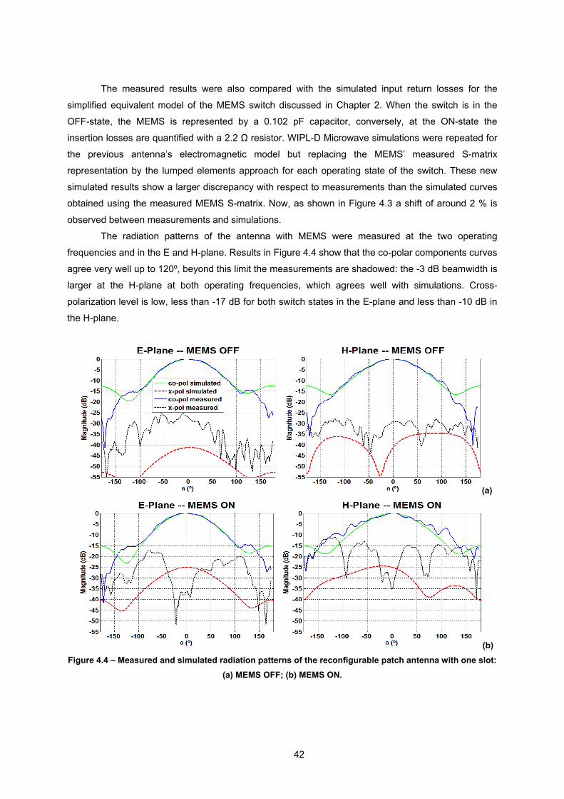
The measured results were also compared with the simulated input return losses for the
simplified equivalent model of the MEMS switch discussed in Chapter 2. When the switch is in the
OFF-state, the MEMS is represented by a 0.102 pF capacitor, conversely, at the ON-state the
insertion losses are quantified with a 2.2 Ω resistor. WIPL-D Microwave simulations were repeated for
the previous antenna’s electromagnetic model but replacing the MEMS’ measured S-matrix
representation by the lumped elements approach for each operating state of the switch. These new
simulated results show a larger discrepancy with respect to measurements than the simulated curves
obtained using the measured MEMS S-matrix. Now, as shown in Figure 4.3 a shift of around 2 % is
observed between measurements and simulations.
The radiation patterns of the antenna with MEMS were measured at the two operating
frequencies and in the E and H-plane. Results in Figure 4.4 show that the co-polar components curves
agree very well up to 120º, beyond this limit the measurements are shadowed: the -3 dB beamwidth is
larger at the H-plane at both operating frequencies, which agrees well with simulations. Cross-
polarization level is low, less than -17 dB for both switch states in the E-plane and less than -10 dB in
the H-plane.
(a)
(b) Figure 4.4 – Measured and simulated radiation patterns of the reconfigurable patch antenna with one slot:
(a) MEMS OFF; (b) MEMS ON.
42
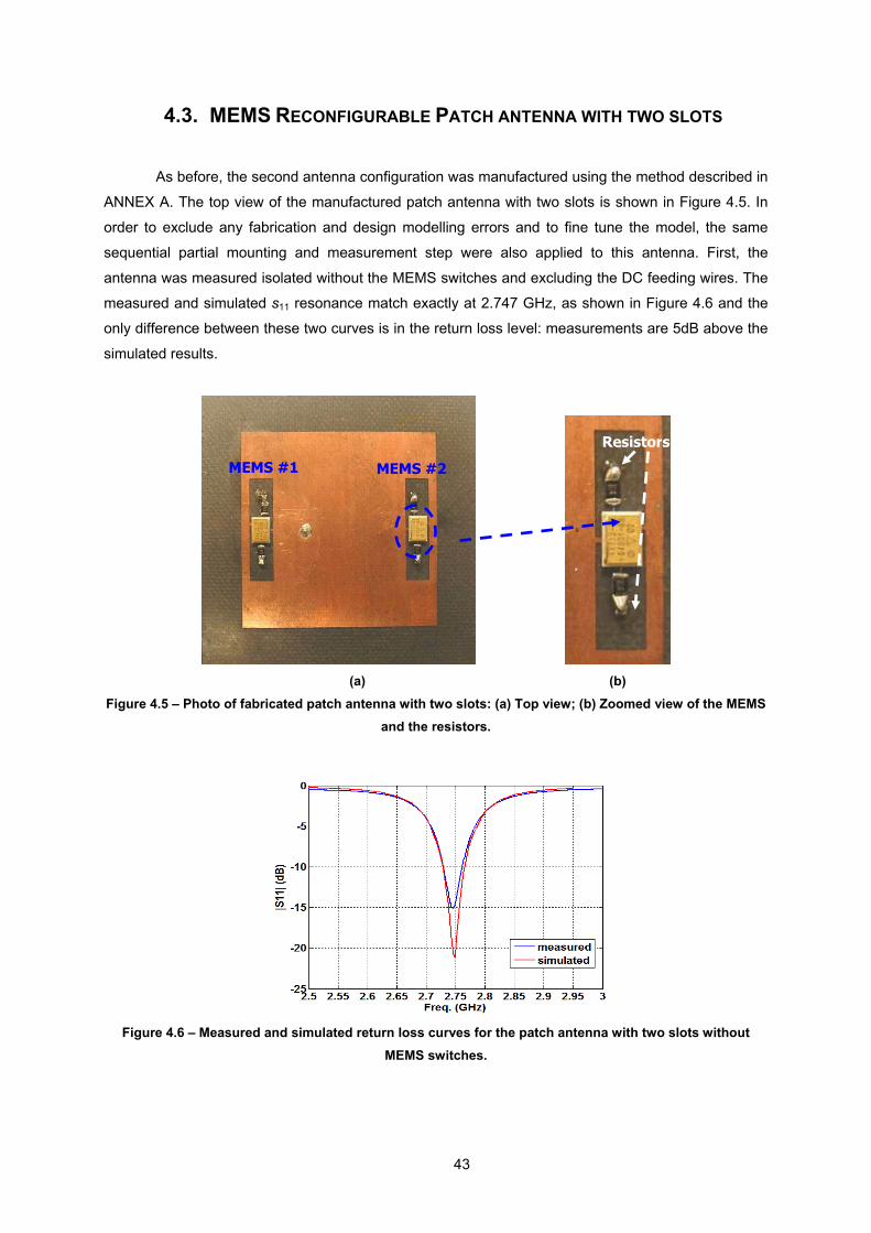
4.3. MEMS RECONFIGURABLE PATCH ANTENNA WITH TWO SLOTS
As before, the second antenna configuration was manufactured using the method described in
ANNEX A. The top view of the manufactured patch antenna with two slots is shown in Figure 4.5. In
order to exclude any fabrication and design modelling errors and to fine tune the model, the same
sequential partial mounting and measurement step were also applied to this antenna. First, the
antenna was measured isolated without the MEMS switches and excluding the DC feeding wires. The
measured and simulated s11 resonance match exactly at 2.747 GHz, as shown in Figure 4.6 and the
only difference between these two curves is in the return loss level: measurements are 5dB above the
simulated results.
Resistors
MEMS #1 MEMS #2
(a) (b) Figure 4.5 – Photo of fabricated patch antenna with two slots: (a) Top view; (b) Zoomed view of the MEMS
and the resistors.
Figure 4.6 – Measured and simulated return loss curves for the patch antenna with two slots without
MEMS switches.
43

Then, only the MEMS #(1) was inserted in the antenna and input return loss was measured. It
was experimentally verified that there were large coupling effects between the RF and DC paths. For
example, simple changes in the DC wires bending or position changed the antenna return loss curve.
This experience revealed that due to the proximity of the RF feed point, the currents that flow through
the MEMS #(1) are higher than the current across the second MEMS of this antenna or across the
MEMS in the previous single-slot configuration. For this reason, it was necessary to include the 100
kΩ resistors in series with the DC lines for both MEMS in order to reduce the coupling effects. For
symmetry reasons, this procedure was performed in both MEMS and not only in the first one. With the
resistors, the measurements appeared to be extremely reliable, repeatable and no coupling effects
were detected. The comparison between measured and simulated input return losses is shown in
Figure 4.7 and in Table 4.2, for each operating state of the switch #1. It can be observe that the input
return losses agree very well, the discrepancy between resonant frequencies is quite good, less than
0.8% for the ON-sate and less than 0.5% for the OFF-state. As before, Figure 4.7 also shows
superimposed on the measurements the simulation results corresponding to the MEMS equivalent
lumped circuits and once again the agreement of this model with measurements are not so good.
(a) (b)
Figure 4.7 - Measured and simulated return loss curves for the patch antenna with two slots and with MEMS #1 inserted: (a) OFF; (b) ON.
Measured Simulated Shift
MEMS OFF 2.675 GHz 2.687 GHz 0.45%
MEMS ON 2.774 GHz 2.795 GHz 0.76%
Table 4.2 - Measured and simulated return loss values of the patch antenna with two slots and with MEMS #1 inserted.
The subsequent and final step was the insertion of the second MEMS into the antenna
prototype with the correspondent resistors in the DC lines and with the DC wires. The measured and
simulated results for the antenna four possible combinations of the two MEMS switching states are
shown in Figure 4.8. As expected from the simulations, it is noted that the antenna produces at least
44

three well defined resonant frequencies (f1, f3 and f4), corresponding to MEMS #1(OFF)-#2(OFF),
#1(ON)-#2(OFF) and #1(ON)-#2(ON). The #1(OFF)-#2(ON) switch state combination produces a faint
resonance, f2.
Again, the numerical and experimental reflection levels at the resonance are very similar.
Even with the increased number of MEMS switches, the discrepancy between measured and
simulated operating frequencies is reasonably low: about 1.1 % for the first three states, MEMS
#1(OFF)-#2(OFF), #1(OFF)-#2(ON) and #1(ON)-#2(OFF); and a 1.8% frequency shift at the fourth
state, when both switches are ON. As verified in the measurement of the antenna with only one RF
MEMS, when this switch is ON the discrepancy between results tends to be larger than when it is
turned OFF.
It is stressed out that the alternative common lumped elements approach to model the MEMS
produces a higher discrepancy in the input return loss characteristic, as shown in Figure 4.8. Results
show that, even though the equivalent model insertion loss and isolation magnitude curves are similar
to measurements in the 2 to 3 GHz band (Figure 2.12 and Figure 2.13), high discrepancies in the
resonance frequency occur due to the different S-Matrix phase values.
(a)
(b)
Figure 4.8 - Measured and simulated return loss curves of the patch antenna with two slots: (a) MEMS #1 in the OFF-state; (b) MEMS #1 in the ON-state.
45

MEMS #1 MEMS #2 Measured Simulated Shift
OFF OFF 2.62 GHz 2.65 GHz 1.15%
OFF ON 2.69 GHz 2.72 GHz 1.12%
ON OFF 2.70 GHz 2.73 GHz 1.11 %
ON ON 2.8 GHz 2.85 GHz 1.78 %
Table 4.3 – Measured and simulated return performance of the MEMS reconfigurable patch antenna with two slots.
Once again, measured and simulated co-polar radiation patterns at these four frequencies
(Error! Reference source not found. and Figure 4.10) show good agreement up to 120º for all
resonance frequencies and planes. The -3 dB beamwidth is larger in the H-plane at all operating
frequencies and agree very well with simulations.
Cross-polarization level is low, less than -20 dB in the E-plane and less than -15 dB in the H-
plane, when switches are both OFF or both ON (the radiation patterns for these states are very
similar). At the #1(OFF)-#2(ON) state the cross-polarization is below -15 dB, except for a small
angular region and at the #1(ON)-#2(OFF) state, the peak cross-polarization increases up to -10 dB in
both planes. Except for the #1(ON)-#2-(OFF) state, the measured cross-polarization levels are higher
than simulation predictions and this is generally worse in the E-plane. This may be related with
induced RF currents in the long DC wires in the measurement set-up.
(a)
(b) Figure 4.9 – Measured and simulated radiation patterns of reconfigurable patch antenna with one slot: (a)
MEMS #1(OFF) - #2(OFF); (b) #1(OFF) - #2(ON).
46

(a)
(b) Figure 4.10 - Measured and simulated radiation patterns of reconfigurable patch
antenna with one slot: (a) #1(OFF) - #2(OFF); (b) #1(ON) - #2(ON).
4.4. PATCH ANTENNA WITH TWO SLOTS USING IDEAL SWITCHES
The two antenna configurations using ideal switches were also manufactured using the
method described in ANNEX A. Once again the objective is to serve as reference to evaluate the
influence of the real MEMS on the antenna performance. The top view of the patch antennas with two
slots are shown in Figure 4.11a and in Figure 4.11b, for the open and closed configurations
respectively. The measured input impedance agrees very well for both configurations and is shown in
Figure 4.12. When the ideal switches are OFF the experimental resonance frequency occurs exactly
at the simulated value of 2.75 GHz. For the ON-state the measured resonant frequency is 2.85 GHz,
corresponding to a shift down of 0.35% comparing with the 2.86 GHz simulated resonance.
47

(a) (b)
Figure 4.11 – Photo of manufactures patch antenna with two slots and ideal switches: (a) (OFF)-(OFF); (b) (ON)-(ON).
(a) (b)
Figure 4.12 – Measured and simulated input return loss of the patch antennas with ideal switches: (a) Open configuration; (b) Closed configuration.
The measured and simulated radiation patterns are shown in Figure 4.13. The co-polar
components are very similar up to ± 120º and the cross-polarization is very low, in both planes and
operating frequencies. Since the simulated results are 50 dB below the co-polarization it is expected
that the measured curves cannot match the very low simulated level but nevertheless the measures
cross-polarization level is comfortably below -25 dB. As predicted by the simulation, the cross-
polarization is higher in the H-plane and results show that at the #1-OFF #2-OFF state the peak is
about 5 dB higher than in the opposite state. This is due to the currents behaviour on the patch; since
the slot is open the currents flow around the slots.
48

(a)
(b) Figure 4.13 – Measured and simulated radiation patterns at E and H-plane for the patch antennas with
ideal switches: (a) Open configuration; (b) Closed configuration.
4.5. EVALUATION OF TICK SUBSTRATE DE-EMBEDDED S-MATRIX
It is recalled that all the previous simulations are based on the MEMS S-matrix that was
obtained from the 10 mils thickness test circuit. The present Section alternatively compares
measurements with simulated results using the measured MEMS S-matrix obtained with the 62 mils
test circuit, equal to the antenna substrate thickness. In this case, the MEMS ports are defined in the
WIPL-D model through wires from the patch to the ground, instead of wires defined over the slot in air
(see Figure 3.2b). In this way, the antenna simulation procedure is in accordance to what is performed
in the de-embedding procedure. The results for all the antenna configurations are shown in Figure
4.14, Figure 4.15 and Figure 4.16. It is observable that, for all the configurations, the frequency shift
obtained for the MEMS in the OFF-state is smaller, but the same does not occur for the ON-state of
the MEMS.
49

Figure 4.14 – Measured and simulated with new S-matrix input return losses for the patch antenna with
one slot.
Figure 4.15 - Measured and simulated with new S-matrix input return losses for the patch antenna with
two slots and with MEMS #1 only.
Figure 4.16 - Measured and simulated with new S-matrix input return losses for the reconfigurable patch
antenna with two slots.
As might be expected, there is a more noticeable discrepancy between measured and
simulated results then what was found with the first de-embedding. This is because the microstrip line
50

is not fully adapted at the MEMS input/output ports as previously noted and because the connector-
line transition is not fully characterized by simulation. However, the main discrepancy occurs at the
ON-state of the MEMS due to the inaccuracy of measurements for this MEMS switch state.
This shows that the simulation model is not as accurate as before because the impedance of
the transmission line influences the MEMS’ S-matrix. To perform a correct de-embedding, the test
circuit lines should be adapted in the measured frequency band.
4.6. GAIN AND RADIATION EFFICIENCY
To try to quantify the radiation losses of the fabricated antenna prototypes due to the MEMS,
two alternative approaches were considered: in one approach the efficiency was calculated through
the ratio of the measured gain to the directivity; in the second approach a direct efficiency
measurement method (to be described next) is adopted.
To infer the part that the MEMS plays in the efficiency value, two antenna prototypes were
compared: the double-slot antenna configuration with MEMS and the same antenna configuration with
narrow metal strips playing as ideal switches. Measured gain, simulated directivity and calculated
radiation efficiency values of the antenna with MEMS at the resonances are shown in Table 4.4: the
slight increase of the antenna gain with the operating frequency is mainly due to the increase of the
antenna directivity. As it can be observed in Table 4.4, the experimental gain values obtained for the
ideal switches configurations are very similar for both switch states but the calculated efficiency is
about 10% higher than for the configuration with MEMS.
The direct approach for the experimental determination of the antenna efficiency follows the
method described in [46] and in [47]. It is based on the Weller cap model [48] and in the closed
waveguide measurements method [49]. Only two impedance measurements for each antenna
configurations are required for this method, one in free space and the other inside a cavity (see
ANNEX D). Appropriate methods for frequency reconfigurable antennas integrating active elements
were not found in literature. The difficulty stems from the need to introduce the MEMS actuation
voltage inside the measurement cavity, but the DC wires inevitably link the supposedly closed cavity
with the outer volume, thus precluding the correct evaluation of the active antenna efficiency. The
results of the active antennas were not repeatable due to non-measurable radiation of the metallic
pieces and DC wires: these measurements presented an uncertainty of around 3% for the radiation
efficiency, which is significant when trying to determine antenna efficiencies in the range
80%85%.The method and detailed results are presented in ANNEX D.
For the patch antennas with MEMS switches #1(OFF)-#2(OFF) and for the antennas with ideal
switches the measured radiation efficiency value obtained with the direct method are in Table 4.4: a
decrease of almost 10% is verified when the two MEMS are included.
For both antenna configurations (double-slot with MEMS or double-slot with ideal switches)
the direct method provides higher efficiency values than those obtained through gain/directivity. This
may be related with the fact that the simulated directivity was used in the first method instead of the
51

calculated directivity due to practical limitations to measure the antenna radiation pattern for all solid
angle
However, both methods agree that when comparing the two antenna configurations, the
MEMS degrade efficiency by approximately 10% (0.5 dB).
#1 #2 Measured
Gain Simulated
Directivity Calculated
Efficiency (G/D) Measured
Efficiency
OFF OFF 4.3 dBi 5.7 dBi 72 % 82 %
ON OFF 4.5 dBi 6.1 dBi 69 % --- MEMS
ON ON 5.6 dBi 6.7 dBi 78 % ---
OFF OFF 6.1 dBi 7.02 dBi 81 % 90 % Ideal
Switches ON ON 6.5 dBi 7.11 dBi 87 % 92 %
Table 4.4 – Directivity, Gain and efficiency of the double-slot antennas.
4.7. CONCLUSIONS
Numerical and experimental results of the antennas show very good agreement, especially for
the input return loss curves, thus confirming the adequacy of the proposed MEMS modelling
procedure. A detailed observation of the results show that the agreement between measurement and
simulation slightly degrades when the MEMS is actuated by the DC control voltage (at the ON-state).
This means that some fine tuning of the modelling may be required in the future for this switch state.
The usual simple approach found in the literature of modelling the MEMS with the lumped
elements deviates the simulated results further more from the measurements and the discrepancy is
larger as the frequency ratio increases. This occurs because the modelling accomplished by the
equivalent circuits does not fully characterize the MEMS switch throughout all the operating
bandwidth, but instead it is calculated at a particular frequency. This kind of modelling is therefore not
appropriate for the optimization of large frequency span antennas, unlike what happens with the
adopted scattering matrix representation of the MEMS.
A considerable effort was dedicated to solving prototyping problems; the technology is
reasonably dominated in the Lab and reliable antennas prototypes with MEMS can now be produced
at IT.
52

Chapter 5 – Conclusions and Future Work
This thesis evaluates the feasibility of modelling a MEMS reconfigurable antenna considering
both the MEMS RF response and its 3D package effects on the final antenna performance, using a
commercial EM solver (WIPL-D). This work is not intended to optimize the antenna performance to
fulfil given specifications for a dedicated application, but rather to test the accuracy of the MEMS
model and evaluate its adequacy for simple and complex configurations, involving one or more MEMS
switches.
For inserting the MEMS switch into the simulation models two types of characterization were
performed: using a dedicated test circuit, the MEMS S-matrix was measured and de-embedded. Then
the effects of its metallic encapsulation, when no actuation voltage is applied to the MEMS, were
measured and demonstrated by the simulation model. Therefore, the model used for the RF MEMS
switch includes its measured S-matrix and the physical description of the package, which are used in
WIPL-D Microwave to combine the 3D EM antenna analysis with a microwave circuit analysis.
Two reconfigurable antenna’s prototypes using MEMS switches have been designed and
manufactured. To develop expertise in the MEMS reconfigurable antenna subject, this work has
53

evolved in incremental steps with full simulation and experimental characterization at each step up to
the creation of fully functional prototypes.
The modelling procedure was developed and tested first on a simple configuration antenna – a
single slot patch antenna with the MEMS switch placed across the slot. In order to assess it adequacy
for arbitrary antenna configurations, the modelling procedure was then blindly applied to a slightly
more complex antenna structure, with two slots and MEMS switches providing four resonances.
The measurements were performed and compared with simulations and good results were
achieved for the input return loss and radiation characteristics. The observable frequency shift was
around 1% for each of the structures. The agreement between measured and simulated co-polar
radiation patterns was quite good while some discrepancies occurred for the cross-polar component,
mainly at the ON-state of the MEMS. Using simple configurations for the antennas, any discrepancies
due to the passive elements were purged and the discrepancies that arisen between numerical and
experimental results were mainly due to inaccuracies of the de-embedding procedure or unexpected
effects on the MEMS behaviour.
To assess for the losses due to the MEMS switches, passive prototypes were simulated and
manufactured. Comparison of peak gain values for the antennas with two slots with and without
MEMS indicated that the MEMS losses decrease the antenna efficiency by at least 10%. Antenna
efficiency was also measured and calculated through a direct method (Wheeler cap) but the two
methods demonstrated a 10% divergence for the radiation efficiency values. The Wheeler cap based
method may not suitable for these antenna configurations due to the occurrence of non-measurable
radiation of the metallic pieces and DC wires inside the cavities and to the DC actuation unfeasibility
within the caps.
In the progress of this work a few experimental impairments had to be overcome. First,
because the contacts of the MEMS are facing down, they provide no access for conventional soldering
to the antenna RF pads. Temperature controlled hot air flux technique had to be used. Upon soldering,
it is not immediately possible to ascertain if all the contacts are well soldered. This can only be verified
measuring the circuit and verifying the reliability of the results.
Regarding the reconfigurable antenna with two slots, one of the MEMS is positioned near the
patch feeding point, where antenna currents are more intense. This was responsible for a few
unpredictable results, such as coupling effects between the RF and DC signals. However, this effect
was overcome with the inclusion of resistors in the DC actuation paths of the MEMS.
Analysing the measured and simulated results a few conclusion can be drawn. First, for an
accurate de-embedding process, the lines that connect to the MEMS ports at the test circuit must
behave as transmission lines to avoid any radiation by the MEMS and lines. If not, when extracting the
MEMS S-matrix from measurements, these effects will have repercussions on the antenna
measurements. This is observable when a wider transmission line was used to measure the switch in
Chapter 4 and the results showed a larger discrepancy with the MEMS at the ON-state. Insertion loss
values are more sensitive to the test circuit characteristics rendering in a less accurate de-embedding
process compared to the MEMS OFF-state. Moreover, even though the equivalent model insertion
54

55
loss and isolation magnitude curves are similar to measurements in the 2 to 3 GHz band, high
discrepancies in the resonance frequency results occur due to different S-Matrix phase values.
The MEMS modelling proposed in this work can be directly extended for higher operating
frequencies, for higher bandwidths and for other more complex MEMS 3D antenna configurations,
where it is likely to outperform even further the equivalent lumped element models for the MEMS
which are limited in bandwidth and which neglect the external effects of its casing.
The goals that were set for this thesis were fully accomplished. It is pointed out that MEMS
switches is an emerging technology and these are still in a development phase, the employment of
these components, packaged or not, for antenna reconfigurability has not been fully demonstrated in
the literature. In this sense the present thesis adds new knowledge in the field. The experimental and
simulated results presented and discussed in this thesis were published and presented at two
conferences, [40] and [41] and one paper was submitted to a Journal [42].
The next step for this work will be to proceed to antenna optimization for real application
specifications with a large frequency ratio (around 2.5) and using a more complex 3D structure for a
more demanding test, such as stacked antennas. Another parallel issue that deserves further study is
the modelling of the MEMS casing influence when it is in the ON-state; the proposed metal box model
is enough for the OFF-state, but it is apparently insufficient for the ON-state.


ANNEXES


ANNEX A Manufacturing process
A.1 Antenna mask
For the manufacturing process, the first step is to design the antenna mask. WIPL-D software
is used for designing the layout and subsequently the structure is printed using wipldmask in black and
white, with the correct vertical and horizontal scale adjustments for printing. Metallic surfaces are
printed in black and the antenna scale normally used is 4:1 or 5:1.
A.2 Photolithographic process
In the next step, the previous mask is transcribed into photographic paper, first in the negative
mode and then this mask in transcribed in the positive mode. This way the manufacturing errors are
reduced, when compared with the method without the negative mode. The machines in Figure A. 1
are used for this process.
(a) (b)
Figure A. 1 – (a) Photographic machine; (b) revealing machine.
59

A.3 Fabrication process
It is necessary to prepare the substrate before starting the fabrication process. First it is
cleaned due to the oxidation induced by the copper and due to thin plastic layer that it is applied for
protection. Then, a photo-sensitive polish is applied and the substrate is dried in the stove shown in
Figure A. 2.
Figure A. 2 – Stove.
After dry, it is exposed to ultra-violet light (Figure A. 3), the photographic mask is applied over
the substrate, in a way that the area to be metallic is not illuminated with the UV light.
Figure A. 3 – Ultra-violet light oven.
This action is performed in an oven with vacuum, so that the positive and negative
photographic papers are well positioned. At naked eye some defects may not be detected, therefore it
is necessary to verify for these flaws using the microscope and correct them, such as white dots.
Then, the substrate is dived into a caustic soda solution. The metal that was previously
illuminated with the UV radiation is now more sensitive and is dissolved. This process takes about 2
minutes at a temperature of 30ºC to avoid burning the circuit.
Finally, the copper that is protecting the substrate is removed in a hiperclorate acid solution for
about 15 minutes and the remaining polish is also detached.
60

ANNEX B Antenna analysis and simulation
B.1 Method of Moments (MoM)
The Method of moments (MoM) or boundary element method (BEM) is a numerical
computational method applicable to problems involving currents on metallic and dielectric structures
and radiation in free space. Is a full wave solution of Maxwell’s integral equations in the frequency
domain, where only the structure in question is discretised, not free space.
It requires calculating boundary values, rather than values throughout the space defined by a
partial differential equation and it is significantly more efficient in terms of computational resources for
problems where there is a small surface/volume ratio. Conceptually, it works by constructing a "mesh"
over the modelled surface. Boundary element formulations typically give rise to fully populated
matrices, meaning that the storage data and computational time will tend to grow according to the
square of the problem size. Compression techniques can be used to ameliorate these problems,
though at the cost of added complexity. However heavily depending on the problem being solved and
on the geometry of the structure in analyse.
MoM is applicable to problems for which Green's functions can be calculated, multilayered
dielectric media, e.g. substrates for microstrip. The special Green's function formulation implements
2D infinite planes with finite thickness to handle each layer of the dielectric. Conducting surfaces and
wires inside the dielectric layers have to be discretised, but not the dielectric planes themselves.
Metallic surfaces and wires can be arbitrarily oriented in the media and are allowed to cross multiple
layers.
For the antenna analysis, the Method of Moments consists in the division of the structure in
analysis in triangular or rectangular shapes. This is done in such a way so that the size of each
segment is at lest a tenth of the wavelength. The definition of the parameters for each segment is very
important, since it influences the precision level of the results. The smaller the elements shape and
greater the number of elements involved, more accurate is the solution. However, a compromise must
exist between the number of elements and their size, since the computational time and memory used
increases with the number of unknowns.
The small elements, in which the surface is divided, are called basis functions and can change
depending of the complexity of the structure in analysis. The method is based on solving the equation:
1
M
i ii
J Jα=
=∑ ,
61

Where J and Ji are the total and basis current density. To solve this equation, boundary
conditions are required to be satisfied at discrete points at the surface, due to the computational
capacity that would be necessary to solve this for all points.
B.2 WIPL-D software
This software package serves fast and accurate design and simulation tool for projects
involving microwave circuits, components, and antennas. Integrating WIPL-D Pro 3D EM solver with
WIPL-D Microwave, it enables easy inclusion of 3D models into the circuit as well as their optimization
from within the circuit.
• WIPL-D EM PRO
WIPL-D Pro (Figure B. 1) is a 3D electromagnetic solver that provides fast and accurate
analysis of arbitrary metallic and dielectric/magnetic structures. Enables to create complex 3D models
using wires, plates and predefined 3D objects as building blocks (Figure B. 2). The Preview window
enables to see how the changes you make influence the model. Also, data defining node coordinates,
wires, plates and other entities can be easily accessed. By defining the coordinates with symbols, it is
possible to control the model dimensions.
Quick and efficient calculations, based on the Method of Moments, yield high-precision results
(distribution of currents over surfaces, near field pattern, far field pattern and circuit parameters).
Figure B. 1 – WIPL-D PRO loading.
62

Figure B. 2 – Example of WIPL-D PRO EM Model.
Application areas include:
• arbitrary 3D antennas and antenna arrays
• transmission lines and waveguides
• multilayered microwave circuits over finite or infinite substrate
• metallic and/or dielectric scatterers of arbitrary shapes
• circuit parameters of multiport structures (Y, Z or S)
• electromagnetic compatibility problems
• WIPL-D Microwave
WIPL-D Microwave (Figure B. 3) enables to accurately extract circuit parameters from 3D EM
analyzed structures. It is possible to use the predefined library, or interactively build composite metallic
and dielectric 3D models. The component library includes closed-form models in 4 implementation
technologies: microstrip, coplanar waveguide, rectangular waveguide, coaxial, lumped elements and
many idealized device models are also available.
It capture allows easy circuit modelling and the import of standard-format data files
(Touchstone) is also supported.
This software helps to develop complex structures as:
• RF and microwave filters,
• Matching structures,
63
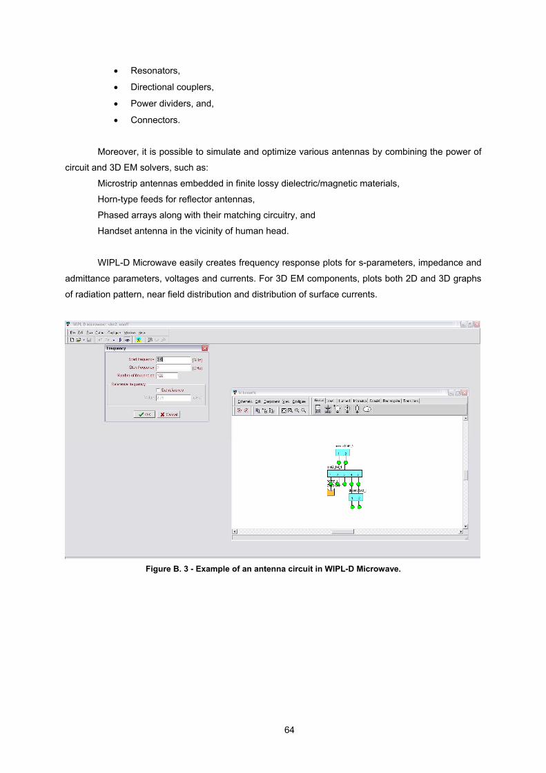
• Resonators,
• Directional couplers,
• Power dividers, and,
• Connectors.
Moreover, it is possible to simulate and optimize various antennas by combining the power of
circuit and 3D EM solvers, such as:
Microstrip antennas embedded in finite lossy dielectric/magnetic materials,
Horn-type feeds for reflector antennas,
Phased arrays along with their matching circuitry, and
Handset antenna in the vicinity of human head.
WIPL-D Microwave easily creates frequency response plots for s-parameters, impedance and
admittance parameters, voltages and currents. For 3D EM components, plots both 2D and 3D graphs
of radiation pattern, near field distribution and distribution of surface currents.
Figure B. 3 - Example of an antenna circuit in WIPL-D Microwave.
64

ANNEX C Study of Patch Antenna Parameters
In this annex, a brief study cornering the influence of parameters of the patch antenna with
one slot shown in Figure 3.2a with dimensions of Table 3.1 but using ideal switches OFF is presented.
The parameters analysed correspond to the ground plane dimensions, patch size (W), feed position
(Xf), slot length (Ls), width (Ws) and position (Ps), and also the influence of the substrate permittivity (εr)
and of the metallic and dielectric losses.
The first parameter analysed is the antenna ground plane and substrate dimensions. From
Figure C. 1 it can be observed that the impedance is barely affected by the dimensions of the ground
plane: mainly is the return loss level that is affected.
Figure C. 1 – Influence of ground plane size in the antenna’s input impedance.
However, concerning the overall dimensions of the patch, W, the resonance frequency shifts
down when the patch is larger and up when smaller, as shown in Figure C. 2. This is due to the
increase or decrease of the total currents path on the patch.
As for the position of the feed along the x-axis direction (Xf), it allows to tune the resonance
frequency and obtain a good impedance match.
65

Figure C. 2 - Influence of patch size in the antenna’s input impedance.
Figure C. 3 - Influence of feed position in the antenna’s input impedance.
The length of the slots (Ls) determines the operating frequency: the input impedance with a
variation of 4 mm in the slots length is shown in Figure C. 4. When this is decreased, the total currents
path is decreased and the resonance frequency is the highest. Conversely, when increased the total
currents path the resonance frequency decreases.
As expected, the same principle of the slot length is applied to the width of the slot (Ws) and to
the slot’s position (Ps), and therefore the same influence on the antenna is verified. Input impedance
results are shown in Figure C. 6 and in Figure C. 7 for the slot’s width and position, respectively.
66

Figure C. 4 - Influence of slot’s length in the antenna’s input impedance.
Figure C. 5 - Influence of slot width in the antenna’s input impedance.
67

Figure C. 6 - Influence of slot’s position in the antenna’s input impedance.
Small variations of 1% in the substrate permittivity (εr ) affect the resonant frequency as shown
in Figure C. 7. However, the loss level is maintained. The higher the permittivity the lower is the
resonance frequency.
Figure C. 7 - Influence of substrate permittivity in the antenna’s input impedance.
Regarding the metallic and substrate losses, the input impedance results are show in Figure
C. 8. It is observable that only the impedance depth is affected by the inclusion or exclusion of the
68

losses in the simulation: when the losses are assessed by the simulation the return loss level
decreases.
Figure C. 8 - Influence of dielectric and metallic losses in the antenna’s input impedance.
69

ANNEX D Radiation Efficiency measurements
The efficiency measurements were performed using the method described in [46]-[47]. Its
principle is very simple and requires only two return loss measurements for each antenna: in free
space and within a cavity. The cavities used for this measurements were dimensioned in work [47]
and can support the frequency range of the antennas proposed in this work: the smaller cavity has a 9
cm diameter and 15 cm length (cavity #1) and the larger cavity has a 14 cm diameter and 20 cm
length (cavity #2), shown in Figure D. 1.
Figure D. 1 – Photo of the two cavities.
For the data processing, a program based on Matlab was developed. This tool receives, in two
different files, the free space return loss measurements as well as measurements with the antenna
inside the cap. The plot of these data in the Smith Chart results in two arcs of circumference, each one
with its radius and centre. Once the center and radius of the cavity measurements is estimated, the
radiation efficiency is calculated using equation (5). minsΔ is the minimum distance between the
resonance frequency and the estimated circumference at the smith chart, maxsΔ is the maximum
distance and 11 fsS is the return loss magnitude at the resonance frequency of the antenna in free
space. These measurements and numerical analyses were performed for the passive antennas with
ideal switches and for the reconfigurable antenna with one and two slots and with the MEMS switches
at the OFF states (Figure D. 2). Due to the isolation requirements for the cavities, it was not possible
to actuate the MEMS switches.
70

21 1max min 11
2 1( ) ( ) 1
r
fss s S
η − −= ⋅Δ + Δ −
(5)
(a) (b) Figure D. 2 – Photo of the inclusion of the antenna prototype within the cavity: (a) front view; (b) side
view.
The return loss measurements for the antenna with two slots and ideal switches OFF is shown
in Figure D. 3. Both measurements on the two cavities are very similar and, in the frequency
bandwidth that enclosures the resonant frequency in free space, no cavities resonances occur. The
radiation efficiency values were obtained using the method previously described and the estimated
circumferences are shown in Figure D. 4 for both cavities. The calculated radiation efficiency is 91 %
and 88 % for the measurements on cavity #1 and cavity #2, respectively.
Figure D. 3 – Input impedance for the antenna with one slot and ideal switches OFF.
71

(a)
minsΔ
maxsΔ
Measured - Free space
Measured – Cavity
Estimated Circumference
Measured - Free space
Measured – Cavity
Estimated Circumference
(b) Figure D. 4 - Smith Charts plots for the patch antenna with two slots and ideal switches OFF: (a) Cavity
#1; (b) Cavity #2.
The return loss measurements for the antenna with two slots and ideal switches ON is shown
in Figure D. 5 . Again, both measurements on the cavities are very similar and in the frequency
bandwidth that enclosures the resonant frequency in free space no cavities resonances occur.
However, small ripple occurs when measuring the antenna on the large cavity. The radiation efficiency
72

values were obtained using the estimated circumferences in Figure D. 6 and are 91 % and 93 % on
measurements within cavity #1 and cavity #2, respectively.
Figure D. 5 – Input impedance for the antenna with one slot and ideal switches ON.
Then, the active configurations with MEMS switches were measured, without being actuated,
inside both cavities. The return loss measurements for the antenna with one slots using a MEMS
switch at the OFF state is shown in Figure D. 7. In the frequency bandwidth that enclosures the
resonant frequency in free space no cavities resonances occurred for measurements on cavity #1.
However, for measurements within cavity #2 a few cavity resonances were verified. The radiation
efficiency values were obtained using the estimated circumferences in Figure D. 8, an efficiency of
87% was obtained using cavity #1 and #2. However, to obtain these values the resonances on cavity
#2 were discarded by the numerical calculation.
73

(a)
(b) Figure D. 6 – Smith Charts plots for the patch antenna with two slots and ideal switches ON: (a) Cavity #1;
(b) Cavity #2
Measured - Free space
Measured – Cavity
Estimated Circumference
Measured - Free space
Measured – Cavity
Estimated Circumference
74

Figure D. 7 – Input impedance for the antenna with one MEMS switch ON.
The return loss measurements for the antenna with two MEMS switches at the OFF state is
shown in Figure D. 9. The radiation efficiency values were obtained using the estimated
circumferences in Figure D. 10 and correspond to 82% and 83% concerning the measurements on
cavity #1 and on cavity #2, respectively. To obtain this efficiency values the number of points used to
estimate the circumference were reduced, due to the proximity of the cavity resonances to the
operating frequency of the antenna measured in free space, especially at cavity #2.
75

(a)
(b)
Measured - Free space
Measured – Cavity
Estimated Circumference
Measured - Free space
Measured – Cavity
Estimated Circumference
Figure D. 8 - Smith Charts plots for the patch antenna with one MEMS switch OFF: (a) Cavity #1; (b) Cavity #2
76

Figure D. 9 - Input impedance for the antenna with two MEMS switches at the OFF state.
Observing the results, the measurements using cavity #1 are more reliable than cavity #2.
When no MEMS switches are included, the radiation efficiency is around 91 %, when one MEMS
switched is included a decrease of 4 % is observed and with two MEMS the decrease is about 8%
when compared with ideal switches.
However, when measuring the active antennas within the cavities a few resonances occurred
and the circumference estimation was limited by the number of points used, especially for the antenna
with two MEMS inside cavity #2. The uncertainty of these results is around 3% and due to radiating
effects of the MEMS encapsulation and DC wires, the measured results were not always reliable or
repeatable, especially for the double-slot antenna.
77

78
(a)
(b)
Measured - Free space
Measured – Cavity
Estimated Circumference
Measured - Free space
Measured – Cavity
Estimated Circumference
Figure D. 10 - Smith Charts plots for the patch antenna with two MEMS switches OFF: (a) Cavity #1; (b) Cavity #2

REFERENCES
[1] WIPL-D: http://www.wipl-d.com/
[2] Teravicta: http://www.teravicta.com/
[3] Project R-Meta: http://www.it.pt/project_detail_p.asp?ID=528
[4] Yang, F., Rahmat-Samii, Y., “Patch antenna with switchable slots (PASS):
reconfigurable design for wireless communications”, Antennas and Propagation Society International
Symposium, IEEE, Vol. 1, June 2002, pp. 462 – 465.
[5] Yang, F., Rahmat-Samii, Y., “Patch antennas with switchable slots (PASS) in wireless
communications: concepts, designs, and applications”, Antennas and Propagation Magazine, IEEE,
Vol. 47, No. 2, April 2005, pp. 13 – 29.
[6] Nanbo, Jin, Yang, F., Rahmat-Samii, Y., “A Novel Reconfigurable Patch Antenna with
both frequency and polarization diversities for wireless communication”, Antennas and Propagation
Society International Symposium, IEEE, Vol. 2, June 2004, pp.1796 – 1799.
[7] Yang, F., Rahmat-Samii, Y., “A single layer dual band circularly polarized microstrip
antenna for GPS applications”, Antennas and Propagation Society International Symposium, IEEE,
Vol. 4, June 2002, pp. 720 – 723.
[8] Yang, F., Rahmat-Samii, Y., “A compact dual band circularly polarized antenna design
for Mars rover mission”, Antennas and Propagation Society International Symposium, Vol. 3, June
2003, pp. 858 – 861.
[9] Shynu, S. V., Augustin, G., Aanandan, C. K., Mohanan, P., Vasudevan , K., “A
reconfigurable dual-frequency slot-loaded microstrip antenna controlled by PIN diodes”, Microwave
and Optical Technology Letters, Vol. 44, No. 4, February 2005, pp. 374-376.
[10] Sung, Y.J., Kim, B.Y., Jang, T.U., Kim, Y.-S., “Switchable triangular microstrip patch
antenna for dual-frequency operation”, Antennas and Propagation Society International Symposium,
Vol. 1, June 2004, pp. 265 – 268.
[11] Medeiros, C. R., Castela, A., Costa, J.R., Fernandes, C.A., " Evaluation of Modelling
Accuracy of Reconfigurable Patch Antennas ", Proc Conf. on Telecommunications - ConfTele ,
Peniche , Portugal , Vol. 1 , pp. 13 - 16 , May 2007.
[12] Medeiros, C. R., Castela, A., Antenas Reconfiguráveis para multi-serviços, Final Year
Project, Instituto Superior Técnico, Lisboa, Portugal, 2006.
[13] Shynu, S. V., Augustin, G., Aanandan, C. K., Mohanan, P., Vasudevan , K.,
“Development of a varactor-controlled dual-frequency reconfigurable microstrip antenna”, Microwave
and Optical Technology Letters, Vol. 46, No. 4, August 2005, pp.375-377.
79

[14] Shynu, S. V., Augustin, G., Aanandan, C. K., Mohanan, P., Vasudevan, K., “Triple Slot
Arm Reconfigurable Dual Frequency Microstrip Antenna Using Varactors”, Antennas and Propagation
Society International Symposium, Vol. 2B, July 2005, pp. 609 – 612.
[15] Onat, S., Alatan, L., Demir, S., “Design of triple-band reconfigurable microstrip
antenna employing RF-MEMS switches”, Antennas and Propagation Society International
Symposium, Vol. 2, June 2004, pp.1812 – 1815.
[16] Lee, A.W.M., Kagan, S.K., Wong, M., Singh, R.S., Brown, E.R., “Measurement and
FEM modeling of a reconfigurable-patch antenna for use in the wideband gapfiller satellite system”,
Antennas and Propagation Society International Symposium, Vol. 1, June 2003, pp. 379 – 382.
[17] Zhang, C., Yang, S., Pan, H. K., Fathy, A., El-Ghazaly, S., Nair, V., “Development of
Reconfigurable Mini-Nested Patches Antenna for Universal Wireless Receiver Using MEMS”,
Antennas and Propagation Society International Symposium, Vol. 1, July 2006, pp. 205-208.
[18] Liu, S., Lee, M., Jung, C., Li, G.P., Flaviis, F., “A Frequency-Reconfigurable Circularly
Polarized Patch Antenna by Integrating MEMS Switches”, Antennas and Propagation Society
International Symposium, Vol. 2A, July 2005, pp. 413 – 416.
[19] Liu, S. Lee, M., Bachman, M., Li, G.-P., De Flaviis, F., “A Frequency-Selectable Patch
Antenna of Circular Polarization with Integrated MEMS Switches”, IEEE Wireless Communications
and Applied Computational Electromagnetics, April 2005, pp. 195-198.
[20] Kunda, V.K., Ali, M., “Reconfigurable Stacked Patch Antenna for Satellite and
Terrestrial Applications”, Topical Conference on Wireless Communication Technology, IEEE, October
2003, pp. 152-153.
[21] Ali, M., Sayem, A., Kunda, V. K., “A Reconfigurable Stacked Microstrip Patch Antenna
for Satellite and Terrestrial Links”, Transactions on Vehicular Technology, IEEE, Vol. 56, Issue 2,
March 2007, pp. 426-435.
[22] Chen, Q., Kurahashi, M., Sawaya, K., “Dual-mode Patch Antenna with PIN Diode
Switch”, 6th International Symposium on Antennas, Propagation and EM Theory, IEEE, November
2003, pp. 66-69.
[23] Ngamyanyaporn, P., Krairiksh, M., “Switched-beam single patch antenna”, Electronic
Letters, Vol. 38, Issue 1, Jan. 2002, pp. 7-8.
[24] Zhang, S., Huff, G.H., Feng, J., Bernhard, J.T., “ A Pattern Reconfigurable Microstrip
Parasitic Array”, IEEE Transactions on Antennas and Propagation, Vol. 52, No.10, Oct. 2004, pp.
2773-2776.
[25] Nishiyama, E., Hisadomi, R., Aikawa, M, ”Beam controllable microstrip antenna with
switching diode”, Antennas and Propagation International Symposium, IEEE, July 2006, pp. 2337-
2340.
[26] -Song Yang, Bing-Zhong Wang, Yong Zhang Xue, “Reconfigurable Hilbert curve patch
antenna”, Antennas and Propagation Society International Symposium, IEEE, vol. 2B, pp. 613-616,
July 2005.
80

[27] Zhang, Y., Wang, B., Yang, X., Wu, W., “A fractal Hilbert microstrip antenna with
reconfigurable radiation patterns”, Antennas and Propagation Society International Symposium, IEEE,
vol. 3A, July 2005, pp. 254-257.
[28] Weedon, W.H., Payne, W.J., Rebeiz, G.M., “MEMS-switched reconfigurable
antennas”, Antennas and Propagation Society International Symposium, Vol. 3, July 2001, pp. 654 –
657.
[29] Jung C., Lee, M., Li, G., De Flaviis, F., “Reconfigurable Scan-Beam Single-Arm Spiral
Antenna Integrated With RF-MEMS Switches”, IEEE Transactions on Antennas and Propagation, Vol.
54, No.2, Feb. 2006, pp. 455-463.
[30] Anagnostou, D.E., Guizhen Zheng, Chryssomallis, M.T., Lyke, J.C., Ponchak, G.E.,
Papapolymerou, J., Christodoulou, C.G., “ Design, Fabrications, and Measurements of an RF-MEMS-
Based Self-Similar Reconfigurable Antenna”, IEEE Transactions on Antennas and Propagation, Vol.
54, No.2, Feb. 2006, pp. 422-432.
[31] Onat, S., Alatan, L., Demir, S., Unlu, M., Akin, T., “Design of a Re-Configurable Dual
Frequency Microstrip Antenna with Integrated RF MEMS Switches”, Antennas and Propagation
Society International Symposium, Vol. 2A, July 2005, pp. 384 – 387.
[32] Petit, L., Dussopt, L., Lahuerte, J.M, “MEMS-Switches Parasitic-Antenna Array for
Radiation Pattern Diversity”, IEEE Transactions on Antennas and Propagation, Vol. 54, No.9, Sept.
2006, pp. 2624-2631.
[33] Coutts, G., Mansour, R., Chaudhuri, S., “A MEMS-Based Electronically Steerable
Switched Parasitic Antenna Array”, Antennas and Propagation Society International Symposium, Vol.
2A, July 2005, pp. 404-407.
[34] Huff, G., Bernhard J., “Integration of Packaged RF MEMS Switches With Radiation
Pattern Reconfigurable Square Spiral Microstrip Antennas”, IEEE Transactions on Antennas and
Propagation, Vol. 54, No. 2, Feb. 2006, pp. 422-432.
[35] Panaïa, P., Luxey, C., Jacquemod, G., Staraj, R., Kossiavas, G., Dussopt, L.,
Vacherand, F. and Billard, C. “MEMS-Based Reconfigurable Antennas”, IEEE International
Symposium on Industrial Electronics, Vol. 1, 2004, pp. 175-179.
[36] Panaïa, P., Luxey, C., Jacquemod, G., Staraj R.; Petit, L.; Dusspot, L.; “Multistandard
Reconfigurable PIFA Antenna”, Microwave Optical and Technology Letters, vol. 48, No.10, October
2006, pp. 1975-1977.
[37] Rebeiz, G, Muldavin, J., “RF MEMS Switches and Switch Circuits”, IEEE Microwave
Magazine, December 2001, pp. 59-71.
[38] Dimitrakopoulos, N., Hartley, A., Miles, R. and Pollard, R., “Microwave Simulation of
an X-Band RF MEMS Switch”, 1st EMRS DTC Technical Conference, Edinburgh, UK, May 2004.
[39] Milosavljevic, Z., “RF MEMS Switches”, Microwave Review, Vol.10, No.1, 2004
[40] Medeiros, C. R., Costa, J.R., Fernandes, C.A., Kolundzija, B., " Modelling of a MEMS
Reconfigurable Antenna Using WIPL-D ", Proc ESA Antenna Workshop on Multiple Beam and
Reconfigurable Antennas , Noordwijk , Netherlands , Vol. 1 , April 2007, pp. 369 – 372.
81

82
[41] Medeiros, C. R., Costa, J.R., Fernandes, C.A., Kolundzija, B., " MEMS Reconfigurable
Antenna Patch Antenna Analysis Using WIPL-D ", Proc 8th International Symposium on RF MEMS and
RF Microsystems, Barcelona, Spain, Vol. 1, June 2007, pp. 67-70.
[42] Medeiros, C. R., Costa, J.R., Fernandes, C.A., Kolundzija, B., “Modelling of
Frequency Reconfigurable Antennas using RF MEMS Switches”, Microwave Optical and Technology
Letters, SUBMITED August 2007.
[43] Rogers DUROID 5880: http://www.rogerscorporation.com/mwu/pdf/5000data.pdf
[44] Agilent, De-embedding and Embedding S-Parameter Networks Using a Vector
Network Analyzer, Application Note 1364-1, [ONLINE] http://cp.literature.agilent.com/litweb/pdf/5980-
2784EN.pdf.
[45] Pozar, D.M., Microwave Engineering, John Wiley & Sons, 2nd ed., New York, 1998.
[46] Geissler, M., Litschke, O., Heberling, D., Waldow, P., Wolff, I., “An improved method
for measuring the radiation efficiency of mobile devices“, Antennas and Propagation Society
International Symposium, IEEE, Vol. 4, June 2003, pp. 743-746.
[47] Mendes, C., Radiation Efficiency of Small Printed Antennas, Master’s degree
Dissertation, Instituto Superior Técnico, Lisboa, Portugal, 2007.
[48] Wheeler, H.A., “The radiansphere around a small antenna", Proceedings of the IRE,
August 1959, pp. 1325-1331.
[49] Johnston, R. H. and McRory, J. G., “An improved small antenna radiation-efficiency
measurement method", IEEE Antennas and Propagation Magazine, vol. 40, October 1998, pp. 40-48.