elc 106.2 lab 4 - complete response of second order circuits
TRANSCRIPT
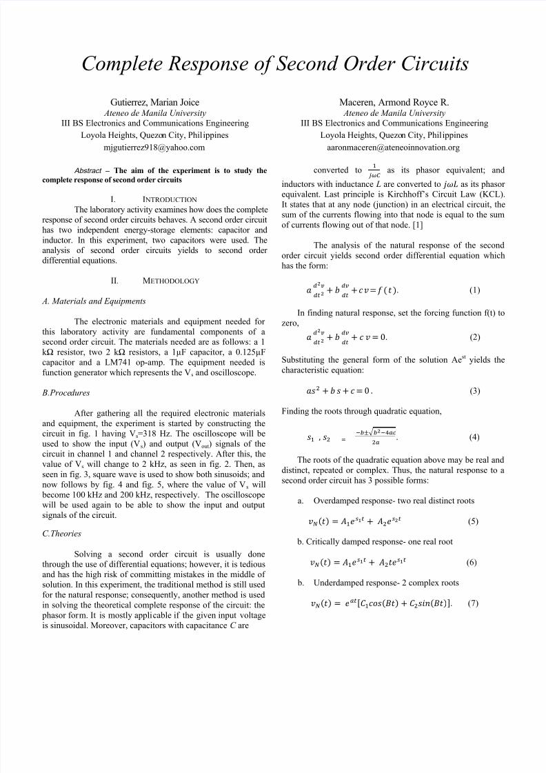
8/12/2019 ELC 106.2 Lab 4 - Complete Response of Second Order Circuits
http://slidepdf.com/reader/full/elc-1062-lab-4-complete-response-of-second-order-circuits 1/3
8/12/2019 ELC 106.2 Lab 4 - Complete Response of Second Order Circuits
http://slidepdf.com/reader/full/elc-1062-lab-4-complete-response-of-second-order-circuits 2/3
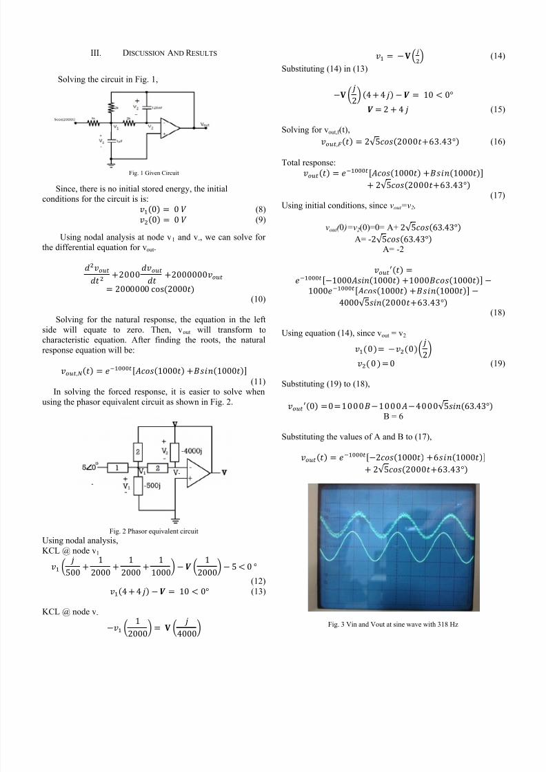
III. DISCUSSION A ND R ESULTS
Solving the circuit in Fig. 1,
Fig. 1 Given Circuit
Since, there is no initial stored energy, the initial
conditions for the circuit is is:
(8)
(9)
Using nodal analysis at node v1 and v-, we can solve for
the differential equation for vout.
(10)
Solving for the natural response, the equation in the left
side will equate to zero. Then, vout will transform to
characteristic equation. After finding the roots, the natural
response equation will be:
[ ] (11)
In solving the forced response, it is easier to solve when
using the phasor equivalent circuit as shown in Fig. 2.
Fig. 2 Phasor equivalent circuit
Using nodal analysis,KCL @ node v1
(
) ( )
(12)
(13)
KCL @ node v-
( ) (
)
(14)
Substituting (14) in (13)
( )
(15)
Solving for vout,f (t),
√ (16)
Total response:
[ ] √
(17)
Using initial conditions, since vout =v2 ,
vout ( 0 )=v2(0)=0= A+ √
A= -√
A= -2
[ ] [ ]
√ (18)
Using equation (14), since vout = v2
( )
(19)
Substituting (19) to (18),
√ B = 6
Substituting the values of A and B to (17),
[ ] √
Fig. 3 Vin and Vout at sine wave with 318 Hz
8/12/2019 ELC 106.2 Lab 4 - Complete Response of Second Order Circuits
http://slidepdf.com/reader/full/elc-1062-lab-4-complete-response-of-second-order-circuits 3/3
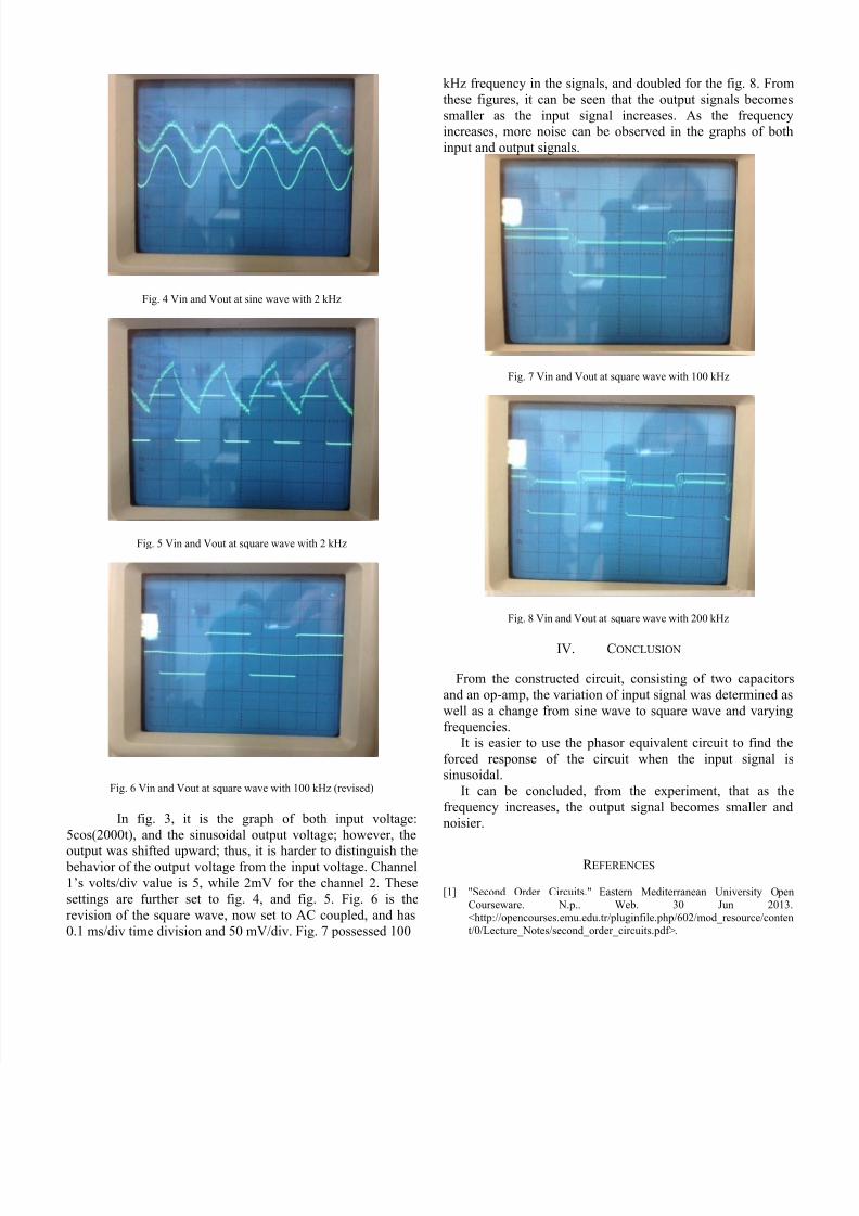
Fig. 4 Vin and Vout at sine wave with 2 kHz
Fig. 5 Vin and Vout at square wave with 2 kHz
Fig. 6 Vin and Vout at square wave with 100 kHz (revised)
In fig. 3, it is the graph of both input voltage:
5cos(2000t), and the sinusoidal output voltage; however, the
output was shifted upward; thus, it is harder to distinguish the behavior of the output voltage from the input voltage. Channel
1’s volts/div value is 5, while 2mV for the channel 2. These
settings are further set to fig. 4, and fig. 5. Fig. 6 is the
revision of the square wave, now set to AC coupled, and has
0.1 ms/div time division and 50 mV/div. Fig. 7 possessed 100
kHz frequency in the signals, and doubled for the fig. 8. From
these figures, it can be seen that the output signals becomes
smaller as the input signal increases. As the frequency
increases, more noise can be observed in the graphs of both
input and output signals.
Fig. 7 Vin and Vout at square wave with 100 kHz
Fig. 8 Vin and Vout at square wave with 200 kHz
IV.
CONCLUSION
From the constructed circuit, consisting of two capacitors
and an op-amp, the variation of input signal was determined as
well as a change from sine wave to square wave and varying
frequencies.
It is easier to use the phasor equivalent circuit to find the
forced response of the circuit when the input signal is
sinusoidal.
It can be concluded, from the experiment, that as the
frequency increases, the output signal becomes smaller and
noisier.
R EFERENCES
[1] "Second Order Circuits." Eastern Mediterranean University Open
Courseware. N.p.. Web. 30 Jun 2013.
<http://opencourses.emu.edu.tr/pluginfile.php/602/mod_resource/conten
t/0/Lecture_Notes/second_order_circuits.pdf>.