el -i f'!f fjf #jl/ g /jl -t j4 #jl i...
TRANSCRIPT

~~x~*~~+*~~~±*A*~~~~
ft El ..g#t : 't-f-?f:(Ol2,022,70I) =!~aM : 90 -i 4 J1 22 a ~ 2 ifi * f'!f .J}1. .8tl : 't -f- FJf 'f #Jl/ G /JL " it ~ -t Jjl it -f-J4 7t/lit #Jl M I IL # 3 ! *tF$-ilt; 1tAA~tttit"!, ~~~ (t;t4) }~t,t~~J:.~f1fi!l,81J~~~#§ Jl:.~.ffl14!!
The following equations are for drain current in a nMOSFET. They may be useful in your answering the following questions.
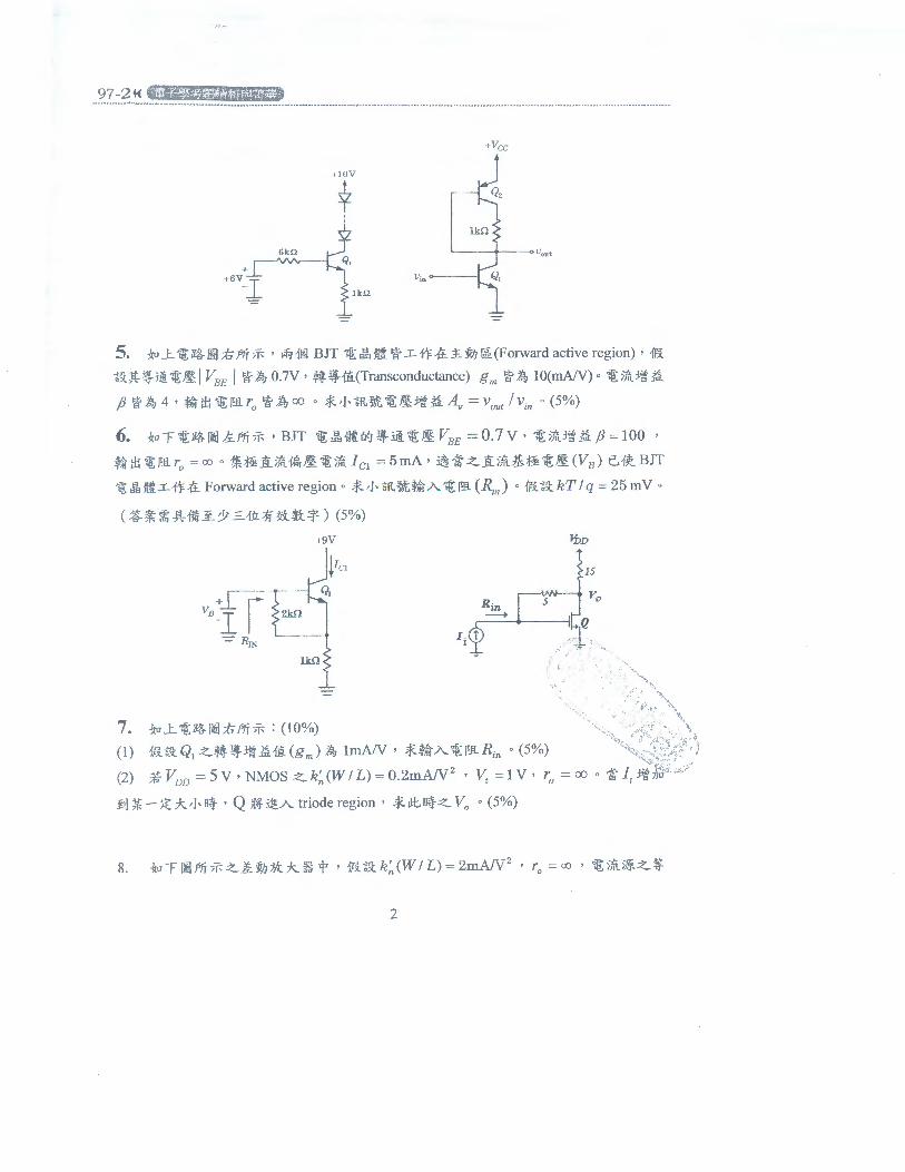
Io(triode)=k0(WIL)n ((V Gs-Vtn)V os-0.5V os2)
l 0 (saturation)=0.5kn(WIL)n (V Gs-V1n)2(1 +AVos)
where kn =J..LnCox· V1n is threshold voltage. The subscript n denotes a n-type MOSFET. A= lN A is the channel length modulation factor.
(1) In the following circuit (Fig. 1), Q2=Q3 (matched), V1n (threshold voltage) =IVtpl=l V; J.lnCox=2J..LpCox=20J!AfV2, (WIL)p=2(WIL)n=l00/10; V An(Early voltage)=!V).ri=40V. Neglect the Early effect for DC analysis and when evaluating the transconductance gm.
(a) Find R to obtain lR=200J..LA. (3%) (b) For the circuit to have maximum small signal voltage gain, find the DC bias VI, the DC output current Im, the mode of operation of Q 1 and Q2, and the small-signal voltage gain of this amplifier. (9%) (c) If the DC bias VI=2V, find the DC output current In 1, the DC output voltage Vo, the Ql and Q2 operation mode. (3%)
\ '!
~· .!'.'
(2) In the following TIL gate (Fig. 2), assume all thansistors arc identical. VBE(active)=0.7V, VBE(saturation)=0.8V, V CE(saturation)=O.l V, t3F=l00, f3R=O.l. fan-out= I.
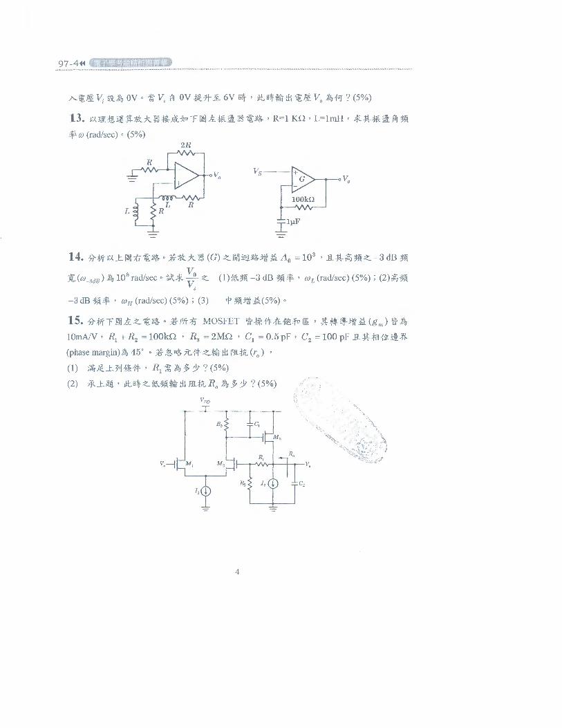
(a) Specify which region (forward-active, reverse-active, off, saturation) each transistor is in when Yin is logic "1 II. ( 4%) ~n~Q11: ~n:l '/aso.n. (b) Specify which region each transistor is in when Vin is logic -I - I r\~u. .... J r.u 11
011
(4%) -- 1---f~ ut"T J"' I n., ~3Sk-l (c) At tJ1e instant when Vin switches from II l" to "0", specify · V;t~____.tf':'t,\-. ~u..- .1. 1;---~ V .. which region the tf::l_nsistor Q 1 &'1d Q6 are in. (2%) • '"' 1 ::. I ..
. I ,): a; (d) If Q6 is removed (i.e., R2 and R5 connected to ground directlv). sketch Vo versus Vin and srecifv the voltages at the break~ints. (6%) • ~ ~ ~- 1- -~' ~: ~~ JKs< ~·J~!
_,'l(QG,
h-,.2 ~
m~~~*•~+•~&4~•A•~~~~
# ~ ..tf! : it-f-:f(Ol2,022 ,701) :!~a 1}} : 90 1f: 4 n 22 a ~ 2 iji
15 f'1t JJ!-8'1 : ·it-T- ffl 'f #Jt! ~ #Jl .. ~t 1f ! J#. it-T-~ 7t 'it ~ll • 2- JL -* 3 Ji *11~Jf.r. ~;t#tfttitil!, $~% (~%) lfi1t:if~J:.zPIT~ll.>J•J~:it1st#~ k~;ffl11-!!
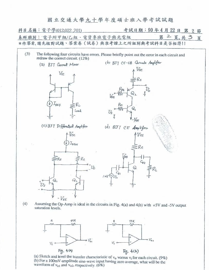
(3) The following four circuits have errors. Please briefly point out the error in each circuit and redraw the correct circuit. ( i2%)
( U) BJT Ckt~ ~imr (b; 8JT CE-C6 C1.r~ ~l.frer
Vee
Re
{d) 8J7 C E .J,,t.-j-e,.. ~c
86
(4) Assuming the Op-Amp is ideal in the circuits in Fig. 4(a) and 4{b) with +5V and -5V output saturation levels.
no· +<~ ~- +<") (a) Sketch and level the transfer characteristic of v0 versus vi for each circuit. (9%) (b) For a lOOmV-amplitude sine-wave input having zero average, what will be the waveform of V0 t and V0 2, respectively. (6%)

~~~~A*~±*~£~±~A*~~~~
ft ~ ..tjt: ~-f-:f{Ol2,022,701} :f~ a JtJJ : 90 1f- 4 A 22 a ~ 2 !e tm•m=t-r~~w~~~t••••-r~~ttt J 3 !,*3 • * f1: ~ }j\r' 1t 7\:J~ ft~,t! ~ ~ ~ ~ ( iit.f.) 1!- ift~t1CJ:.~ffl ilt})IJ ~~~# El k 1i {a 14! !
(5) In Fig. 5, the Op-Amp is ideal but with the input offset voltage V 05• The power supply voltages of the 0p-Amp are +5V and -5V.
(a) Assume that VI=0.5V, Vz:::::l V and Vos=:OV. If the switch S is closed, calculate Vo. ( 4%) (b) The same as in (a) but with the switch S open and 1-negJigible switch transients, calculate Vo. (4%) : V, +
(c) The same as in (a) but with Vos=+5mV, calculate Vo. (4%)
'
(6) The following circuit (Fig. 6) shows a feedback amplifier,
(7)
(a) Identify the feddback topology of the above amplifier. Calculate the feedback factor fl (7%) ---------1
~
(b) Identify the feedback type, positive or negative feedback? + why? (3%)
(c) Replace the NMOS device Q3 by a pMOS device and keep all other circuits unchanged Draw the PMOS Q3 amplifier stage. Identify the feedback type. (5%)
In the following CMOS inverters, assume the k and WIL of ail nMOSFEfs and pMOSFETs are the same . V m==0.8V and Vtp=-0.8V. A=O Voo ~ SV
'
= -(a) Determine the range of V0 1 for which Nl and PI are biased in the saturation region. (5%) (b) IfVo2=0.6V, determine the values ofV03, Vol and VI. (10%)
~iLxi!J\.*JL+
ft §~{if it-t--:¥-{012, 022, 901) ~ti\: 81JJ : 91 !f- 4 tJ 20 8 ' 2 ~
~ffl*'N -t-t-.x..f£$~ fili/~m · 'tJi-!*'1-1-1!-:Jt't~ll ¥ JL # 3 ! * 1'¥ $ JJ.i, tt *:A~ tt~::l! · $ ~% ( ~%) ~ ;jt J;-~J:..:<..P!T jllJi'l ~ ~ t.~At E1 k ~{a -71-! !
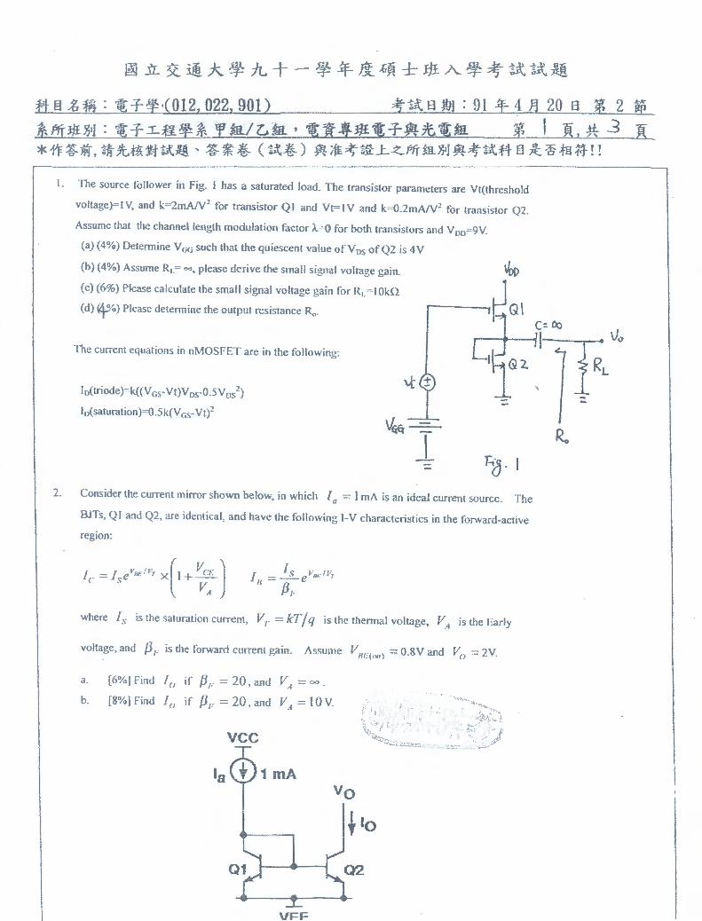
I. The source follower in Fig. I has a saturated load_ The transistor parameters are Vt(threshold
voltage)= ! V, and k=2mAN2
for transistor Ql and Vt= IV and k={)_2mAN1 for transistor Q2.
Assume that the channel length modulation factor A.=O for both transistors and V0D=9V
(a) (4%) Determine V GG such that the quiescent value of V 05 ofQ2 is 4V
(b) (4%) Assume RL = oo, please derive the small signal voltage gain.
(c)(6%) Please calculate the small signal voltage gain for R1. = I Okn
(d)~) Please detennine the output resistance R., .
The current equations in nMOSf-ET are in the following:
lo(triode)=k((V Gs-Vt)V 05-0.5V0 s ::?.)
10 (saturation)=0.5k(V Gs-Vt)2
v~ -..L..
_I 1J· I
2. Consider the current mirror shown below, in which I a = I rnA is an ideal current source. The
BJTs, Q I and Q2, are identical, and have the following 1-V characteristics in the forward-active
region:
where Is is the saturation current, V,. = kTj q is the thermal voltage, VA is the Early
voltage, and {3 1_. is the forward current gain. Assume V1u:
1.,
11, = 0.8V and V
0 = 2V
a. [6%J Find 111 if {3,.. = 20, and VA = oo .
b. [8%] Find 10 if {3,.. = 20, and VA = l 0 V. ;; ..
vee
mA
VFF
R ..
fHL~i~ 't-1--¥:(012, 022, 901) 5-tA:. 8 ~A : 91 !f. 4 J1 20 8 ' 2 ~ ~ r!T Jj!Ji'l 't + .L;f£ :¥= ~ ! m/ 0 ilL ' 1:! -!J.jlit +~ 7\:.1: ~Ji 5f> .L 1i:, # J }! * 1t~m-, tt~A~tttA'.~ , % ~ ~ c tA:~) ~;it~~J:.--t..rn- m>i~J ~~tA'.# EI k 1I .fl311-'!
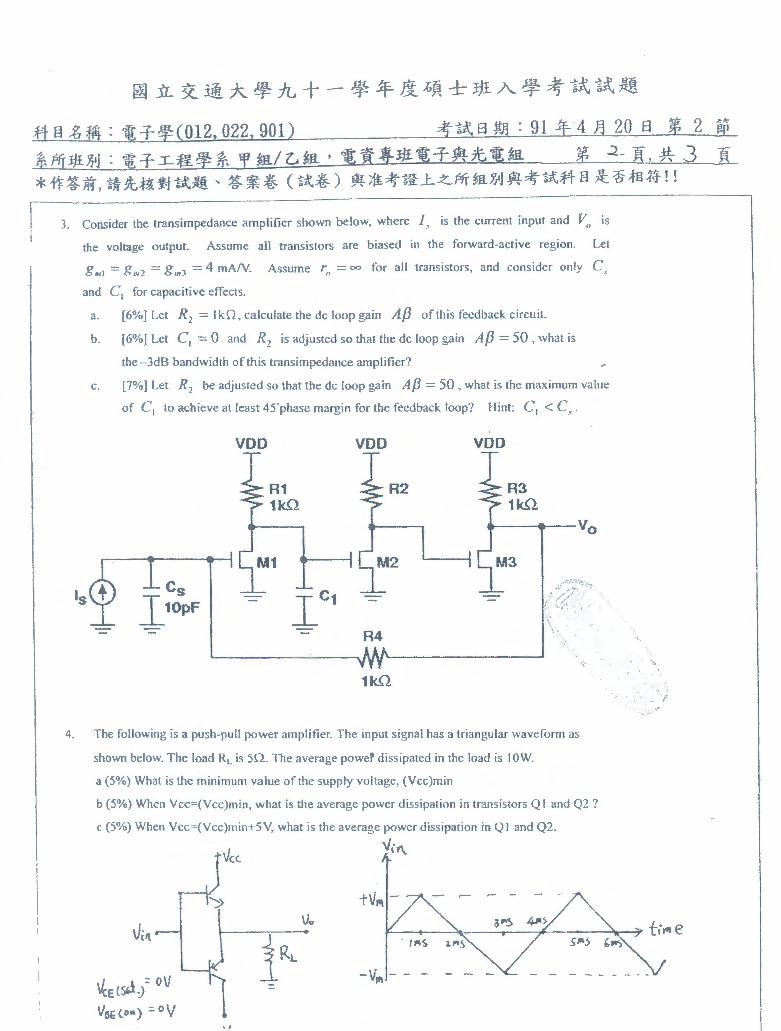
3. Consider the transimpedance amplifier shown below, where I, is the current input and V, is
the voltage output. Assume all transistors are biased in the forward-active region. Let
g 1111 = gm"2 = g,J = 4 mA/V. Assume r, = oo for all transistors, and consider only C,
and C1 for capacitive effects.
a. [6%] Let R2 = I k 0, calculate the de loop gain A[J of this feedback circuit.
b. [6%] Let C 1 = 0 and R2 is adjusted so that the de loop gain A[J =50, what is
the - 3dB bandwidth of this transimpedance amplifier?
c. [7%] Let R2 be adjusted so that the de loop gain A[J =50, what is the maximum value
of cl to achieve at least 45"phase margin for the feedback loop? Hint: cl < C,.
VOD T
R1 1k.Q
VDD
R4
11<.0.
R3 1k.Q
,.,. ;.~, ..... ' . . :.- t;
,) ,.:' I' • ~
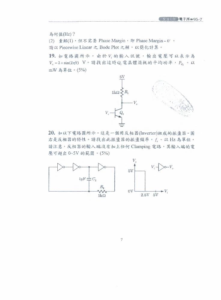
4. The following is a push-pull power amplifier. The input signal has a triangular waveform as
shown below. The load RL is 5D.. The average powe1 dissipated in the load is I OW.
a (5%) What is the minimum value of the suprly voltage, (Ycc)min
b (5%) When Vcc-=(Vcc)min, what is the average power dissiration in transistors Q I and Q2?
c (5%) When Vcc=(Vcc)min+5V, what is the average power dissipation in Q l and Q2.
'hJ\.
-v,..- - -
,,

't-1-¥-{012, 022, 901) 5~ 8 fi.JJ : 91 -! 4 J1 20 8 ' 2 ~
5. A CMOS astable circuit is shown in the following. Clamping diodes are connected at the input
terminals to prevent the input signal from rising above V00+V0 and falling below - V0 (Vn is ihe
diode voltage drop). Assume ~m<<R and Y,h=0.5Y00 where R0~ ;md V,h arc the output
resistance and the threshold voltage of the CMOS gates respectively.
a. (6%) For Y n"'OY (Clamping diodes arc assumed ideal), sketch the waveforms of Y ll· Y 01
andY 02 and derive the period T Is the period T a function of V oo?
b. (6%) Repeat (a), but now for V 0 =0.5V, is the period T a function of Y 00 ?
R
c .......
L----------------+----~t--~
6. A circuit of a NAND gate is shown below. Inputs A and Bare connected. Assume 13~=30, f3R=O.l,
VsE(sai)=O.SV, VcE<satJ=0.2V and neglect leakage currents.
a. (5%) For Yr=OV, find numerical values for 101 , 102 , 103 and Yo
b. (3%) Estimate a numerical value for Y1 when V 0 switches to logic zero.
c. (14%) For Y1=4.5Y and use Y0c 1=0.6V, find otHnerical values for In" ls2, ln. 11n, ICJ and
Yo and determi;1e the region of operation for Q I, Q2 and QJ.
l I ~lo~D. I· Io: (He,
--~-, Q).
::
I~lj ~

:i •j ;l ,l ~ ;
!
H 8 .tft : 'i!lr* C 012 • 022 • AJO :tf~B.mL_92¥4§20B 5f~2ffi!
~ Jifr$:8'1 : ' 'lf-ffilf'il!ZM! · 'l!iiW:filllt!Ji!J\:itU§ s; \ . Ji ~ # 3
(I}Considerthe following circuit and its input waveform V1 shown below.
(a) [6%] Draw the V0
wavefonn. Assume the operational amplifier is id.eal, and without input offset
voltage and bilas current, i.e., V0s = 0 V and I 8 = 0 rnA . (b} [7%J Draw the V., waveform. Assume the operational amplifier is ideal, except that it has a non-zero
input offset voltage, i.e., V os = 0.5 V and I 8 = 0 rnA. \ . (c) [7%] Draw the ~ waveform. Assume the operational ampHfter is ideal, except that it has a non-zero
input bias currtllt, i.e., 18 = 0.5 rnA and V os = 0 V.
Vt (Volt)
R1 +2
+1
Cj Ia 11&
vi-; 1J.IF Vo. Vo (Volt}
-
4 • • ~ - - ~ · 1 msec · 1 msec · 1 msec ·
\ \~·- ' > ,' ;' '~ {(,,1
(2) In the following circuit, the current equation for a MOSFET in saturation region i:~to~sk(v~~:~)'~. VtCnMOS)= -V1(pMOS)=2V, k(nMOS)=k(pMOS}=50~2• R=lOMfl and Cis sufficiently large.
(a) [6%} What are the DC current and transconductance (g.,) ofQl and Q2?
(b} [100/o) lfV A(Early voltage)=l80V, what is the small signal voltage gain vJv,?
(c:} (4%} For what range of output voltage do Ql and Q2 remain in the saturation region?
Jt(,V r-4~ Q.:t r-TrtJ :~v.
Vs~ ·~· Q' L
-1+'1/
t
t
1

fHLtf~ : m..:_r.~ (Ol2. 022 •. AU) ~ID:tBUD: 92!¥41§20[] ?J12fifj
~ ,Sif JJI>)'J : • W'j-p[f4:#J.tZ:.ffH · 11l::tiWiii1f~-T~!W~f1l*ll _ ~~ ]_ _1C ft. 3 ! * 11" ~ !1, 1t ;\:.H~ 1-t tsi.M .. ~ ~% ( ti\:4 ) ~ ;jt ~t~LJ:. .:<:-M ~Jt jjtJ W- ~-L\ fl g it~~! -1·1- ! !
(J) Consider the amplifier shown below (Fig. 3). Let g.,1=&n2= 5mAN. and g,3 = 2.5 mA/V when switch is
closed. All the MOSFETs are operated in saturation region. Neglect channel length modulation effect .
A. ff switch is open, aruwer the following questions.
(a) f5%J Small signal DC gain VoNi = ?.
(b) [5%] - 3 dB bandwidth ofVo;Vi ~?
B. If switch is closed, answer tlte following questions.
(c) [3%] What kind of feedback topology (shunt-shunt, series-shunt, shunt-series, series-series) is utilized in tiis amplifier ?
(d) [7%] Smafl signal DC gain Vo/Vi = ?.
(e) [5%}-3 dB bandwidth ofVoNi =?
VDD
10k.Q 1k.Q
10nF
c Vi +--j
r 'switch
M3 J t-j --~-...•- + f Vo v v-
Fig. 3
L---:-----___...,_.- - -

~ 8 .£~: mr9! <ot2 , o22. ·AU) :lV~BWl: 92XE4FJ20I3 . %2flli
& fflJ}!.})•J : '1JF1-f;Ilf!WIZ.W. , wt\iWJ[m-I:W2Yiilf.Ml . .. ·' 3 JL 1\ ~ . 1f * <f1 $ ~, tt ;tlt 1t "£tt-l! ~~ ~ ~ _ < 11.~ ) 9! *~ aJ:..:t...ffl#Jl ~·J .9!-~ !X.~ 6 lt ::§-to -f1- • •
(4) A circuit ofMwtooth waveform generator is shewn m Fig.. 4{~) with a Schmitt trigger followed by an
integrator. The limiting levels of the Schmitt trigger are +Vz and -Vo. The output tciangul,a.r wavci'Of1!1 is
shown in Fig. 4(b).
VTH-- --I
I ' I
: I Vn .. ___ -:- ---- ---- r .
~1\lt-- T,. )o[
(a) [l(}QAt.) Find Vn.. Vm. T1 and T2 in tenns ofVz, Vo. R" R2, Rand C.
(b) [S%} For V~.JV, V0=!>.7V, R~1'=3n and RC=2.lxl0-J sec., sketch and level the triangular_
waveform. What is the frequency of oscillation of the circuit ? .-.:·i" . . .. ' ~ ...... ,. '•
lS:···. . ~ ~~::. :;c (S) For the ECL circuit in Fig. 5(a). assume that the base-emitter drop of an ON trans:isror is 0.8\f""a:li(fcut-in--~-
voltage is 0.6V. VM
~\... \hl1 th
---·------
Vo" hd· 5'(~)
Vs
0...
1',.= -l v -Ya(-S.2V) Yr=-2V
~.S'(') J..
(a) [6%] Cal.culate Vu... Voc. Vm, VOH and noise margin NMn and NMc:. of the OR transfer characteristic as
shown in fig. S(b ). Ignoring the base current when cakulating V oc. but using P=99 to calculate Voo.
(b) [4%] Recalculate Va, Voc., Vm, Voo, NMa and NMLwhen the 500 resistor RT isreplaa:dby 50k!l.
(c) {S%] The NOR transfer characteristre is shown in Fig. S(c). It bas four distinct regions as indicated by
segments ab, lx; cd and de. What are the corresponding transistor modes of operation (cut-oft
active or saturation) of Q,.. Qa and Q3 for each segment?
(d) (2%) Explain why the ECL circuit employs a negative power suppty and the Vee line is COMected to ground?
lloti
VoL
~CIIt
~
e
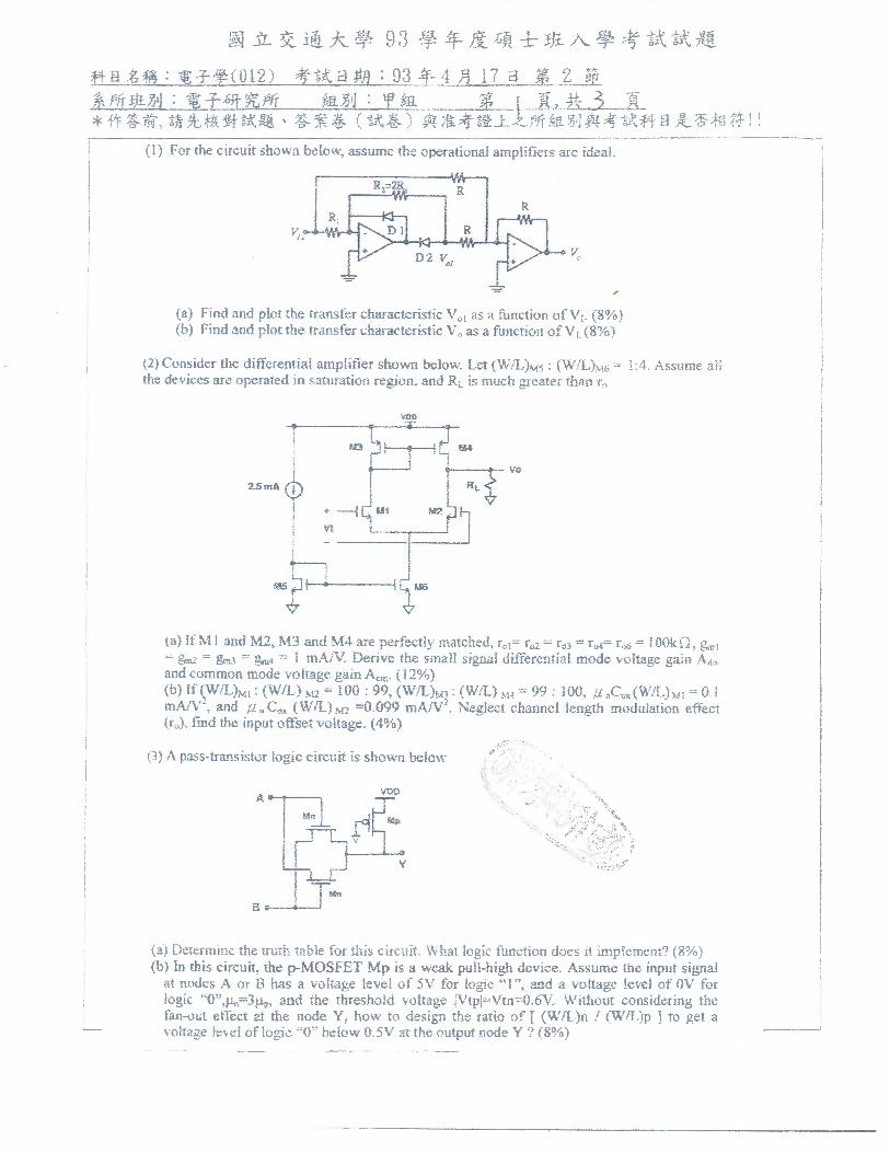
(l) For the circuit shov•<11 bdm.,·, assume th~ opemtional amplifiers are ideal.
~ R I
,
(a) Find and plot the transfer characteristic V01 as a function ofVt. (8%) (b) Find and plot the tran..sfer characteristic Vc as a function ofV1 (8%)
(2) Consider the differential amplifier shown below. Let (\V/L)Ms : (W!Lhto '""'· i :4. Assume ali the devices are operated in saturation region. and R;_ is much greater than :,.
• I i l
25mA ~
vna
t T T
~Fhv• + -- u: f.t1 M2 p ~ VI 'l ! I
t-. J M5 ~ t-! _.l,.__ _ ____, 4, M6
~ ~
{a) lf~ll and r-.n. M3 and M4 are perfectly matched, rc,= r"2 = r~3 = ra-1= r.,o =lOOk~), f5_-r.,
= g"'.: = &n3 = g.,,4 = : mA/V. Derive <he small signal diiferentiaf mode ·voltage gain Adn
and common mode voh.age gain A:.rr.· (12%) (b) If\W/Lh,~: (\Vil.) l\c? = 100: 99, (W/L)~.n: (\V/L ) ~t4 = 99: lOO, I.L nCox(\V.'L.h!· ~~ 0.1 mAfV·, and .u.nC,x (WtL)Mz =0.099 mAN2 ~eglect channel length modulation etlect (r0 ). find the input offset voltage . (4%)
......
t3) A pass-transistor logic circuit is shown be!o·w ,..> (
,•.
.:;_::
\_a) Determii:.:: the truth tab;e for this circuit. \\ihat logic funcrion does it imp!ement"~ (8%j (b) In this circuit, the p-MOSFET Mp is a weak pull-high device. Assume the input signal
at nodes A orB has a voltage level of SV for togic "1", a.'ld a voltage level of OV for logic ·~o··,)J.n=3Jl.o, and the threshold 'vOltage :Vrpj=Vtn=0.6V. Without considering the fan-out effect at the node Y, how to design the ratio of [ (\V/L)n / (WiL)p } to get a 'oltage level of iogic "0" belo\v 0.5\! at the ouiput node Y? (8%)

I !
~ ?fl" J)l >i1] : itt -f-~ 1E F1T * ft: $ fltr, tt ;'cA~ itt~~ ,
(.f) tn the fullO\\ ing C\10S circuus. the current equation in the nMOSFET i~ as follows:
lo=k {Vas-V J" !n=k (2(Yos-Vt)Yns-V,;/)
{saturation region) (triode region)
where k=0.5pC0 x(W/L) and V\ is the threshold voltage of the n\'lOSFET. The current equation in the pMOSFET can be derived likewise. V 00=5V, k(nMOS)=2mA!V2
.
k(p\-fOS)=0.5mAtV:_ V:(nMOS)=0.6V, V,(pMOS)= -0.8V
(a)
~eki~l flr,e
\ ' --- ~
t~ v, v~.J
(b) (C)
{a) For a Cl'vfOS inverter (Fig. (a)). the Yo versus Vi is sho ... vn in Fig. (b). Please calculate the values ofV~, Y:. Y;. V4 . (8%)
(b) In a C:VIOS amplifier (fig. (c)), what is the \aluc of \'\;c that the small-signa! voltage gain A,=vjv, has a largest Yalue ? For RL=lOkO, C=x, what is the maximum small-signal voltage gain? (8%)
(5) Consider the feedback amplifier sh0\\!1 belov •. Assume all ihe ~10SFEE are operated m saturation region, grr: 1 -== gm: = I mA 'V2
•
( \
von
~ 10kQ
-d ' Cp ~Vo1 '" <t-l' 't l M2
1nF t-- Vo2
I ' r I I I cbls I r I
.... v OOkQ. ~1kQ
(a) If the output voltage is taken at V 0 :, which feedback t-ype is adopted !n the ;:;ir(uir lshunt-shunt. shunt -senes, series-shunt. series-series). (3%)
(b) If the output voltage is taken at V02, wh1ch feedback type is adopted in the circuit (shunt -shunt, shunt -series, serics-sbunt, series-series). (3%)
{c) Find the low frequenc) small signa.! gain ofV, 1/f,. (7%) (d) Tf Cp = i nf and neglect a!! the other parasiTic capacitances. Find the -3 dB
bandwidth ofV~~/ls. (7%)
·-----1

~~~~A~93~~&~±*A·~~~~
H § ~ $l : ~ --f #'- ( 0 12 ) ~ t:;:t 8 ~Jj : 9 3 if- 4 J3 1 7 E % 2 ~P
~ fFr #£ ~11 : 't -}--hit 1E P1T jJL~'J : 11 ~Ji jf; ::, J{, # 3 Ji * ft: $1¥J, ~t -ltA~ !tti(~ ' $ ~ Jri- ( t~:/i- ) ~ ;ft~*__t?_z_J'tf fJL~rj ~~~# § lt ~,fa#! ! i------ -·--·- .. --···-··----··-··- ····-··------
, (6) Consider the class B output stage, as shown below. Assume the devices have JV1i=JV, }lC0 ,(WiL)=200mA!V2
, and the load resistance is very high, i.e., Rr-+o::·; +WV
v,~~v, '+'
-!OV
(a) Plot the transfer curve \ 0 versus v, and indicate the input vcltage range and the output voltage range. (8%)
( b) When a bias voltage V G{j is applied bet·ween the gates of the two MOSFETs, the circuit becomes a class AB output stage. What value of V GG is required to reduce the incremental output resistance R, in the quiescent state to l OQ '! (8%}
' .. _;;.•
I
i I i
_____________ ___j
·--
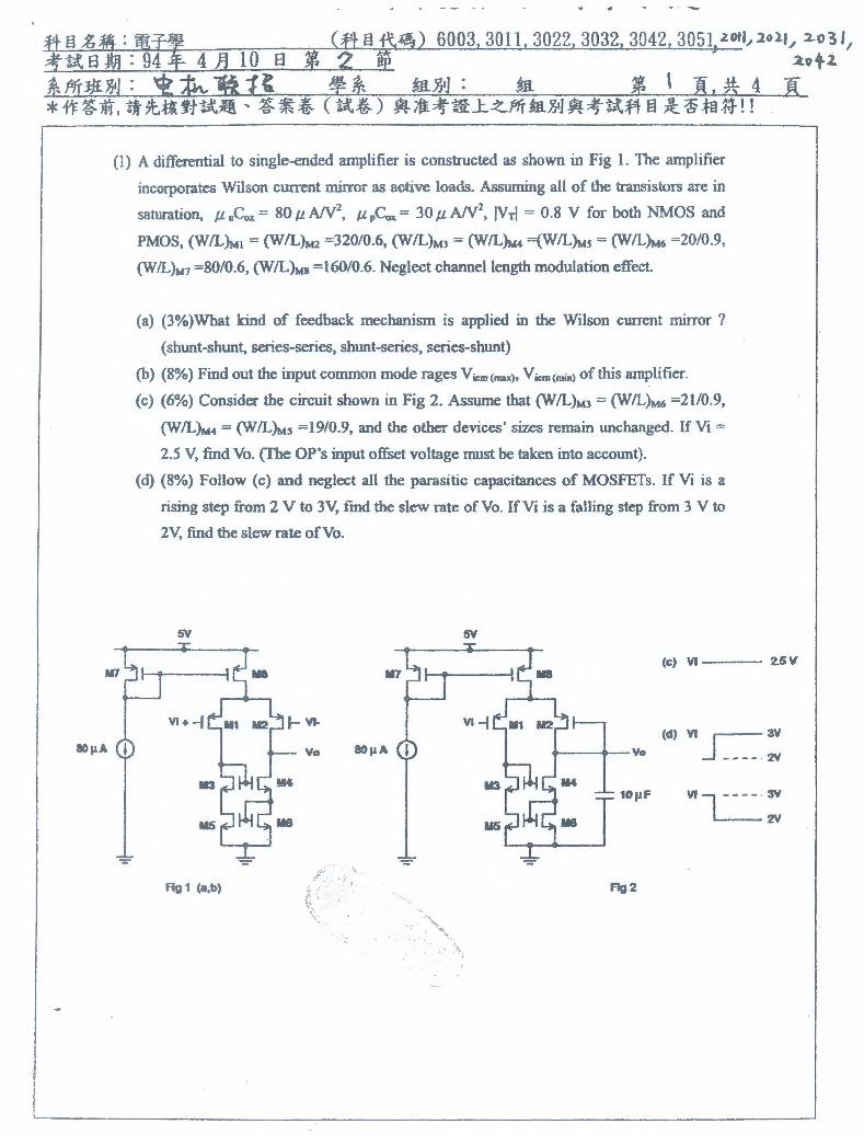
(1) A differential to single-ended amplifier is constructed as shown in Fig 1. The amplifier
incorporates Wilson current mirror as active loads. Assuming all of the transistors are in
saturation, Jl. nCox = 80 Jl. AN2, Jl. pCox. = 30 Jl. NV2, IVTI = 0.8 V for both NMOS and
PMOS, (WIL)M1 = (W/L)M2 =320/0.6, (W/L)M3 = (WIL)M,. =(WIL)Ms = (W/L)M6 =20/0.9,
(WIL)M7 =80/0.6, (WIL)Ms =160/0.6. Neglect channel length modulation effect.
(a) (3%)What kind of feedback mechanism is applied in the Wilson current mirror 1
(shunt-shunt, series-series, shunt-series, series-shunt)
(b) (8%) Find out the input common mode rages Vicm(max), Vicm(min) of this amplifier.
(c) (6%) Consider the circuit shown in Fig 2. Assume that (WIL)M3 = (W/L)M6 =2110.9,
(WIL)M• = (y/IL}Ms =19/0.9, and the other devices' sizes remain unchanged. If Vi =
2.5 V, find Vo. (lbe OP's input offset voltage must be taken into account).
(d) (8%) Follow (c) and neglect all the parasitic capacitances of MOSFETs. If Vi is a
rising step from 2 V to 3V, find the slew rate ofVo. If Vi is a falling step from 3 V to
2V, find the slew rate ofVo.
5V 5V
(c) VI 2.5V
" ·' ' '.
Flg2 ~~. ,.

Lt8 1L 3-t:i@. :Ji;.. ~ H4~ + ~. -lijt ± Jji A~~~~~~
fi ~_g. Mt: 'l:r~ (# El fS.~) 6003,3011,3022,3032,3042, 30516 2°1f,~'2o2.J, ~o3J, ~tt a~ : 94 -! 4 Jl 1 o a 8t 2 iP J.•lf-1.
*fflJJ!~J : 'ft ~.-~ :c :f: * m.&J : m ~ :;_ JL * 4 H * 1f ~ Jlt, 1t 5\:A~ ft"tt:R! .. ~ * ~ (1st~) ~ ;ft~;t..l.~f1f ift.*l ~~~# B Jt ~ {ij 14! !
(2) A two-stage cascade amplifier and its small signal equivalent circuit are shown below.
The first stage is a common source amplifier with source degenerated resistor. The
second stage is a shunt-shunt feedback amplifier. Assume that the MOS has infinite
output resistance. Here &nt=~= 10 mAN, Cgs,=Css2=20 tF, C&d1=Csc12=0 fF, Rsig=45 k!l,
~= 5 k!l, RF 45 kn and R.r5 ill.
The voltage transfer function can be expressed as follows.
A iol ( ) V out ( )
( 1+~](1+_s J = Vsig s i:;- 8
mP, mp2
(a) Please calculate Avo. the de voltage gain. (6%)
(b) Please calculate the first pole,c.op" corresponding the first stage io1Nsi&· (6%)
(c) Please calculate the second pole, c.op2, corresponding to the second stage Vourfio1• (6%)
Note: The effect of gate-to-drain capacitances on the frequency response can be neglected
because the shunt-shunt feedback reduces the input and output impeda_l!Ces of the second J
stage.
' . ,, ;..'•.
l
~ 1L .X i!A ~ 94~ lf-li -b,Ji ± J}1 A~ :lf ~ ~~ ft § _.t{!: ~T~ (#§ft.~) 6003,3011,3022,3032,3042,3051 ,2oll, l.vl.l, 2•311
-!ts\:. a ltlJ : 94 !- 4 A 10 a J 2 !P J. olf.:z. *' rJtJ)!.$'1 : ~ ~ e. 8 1-£ m)JIJ : m ~ 3 J!, *' 4 J! *1f$1W.tt;t.~f.f~,t!" $*4 (~4) 1!-iit~~J:..:t..PJTMI.JJ•l$!.~~#§ Jl1l~1~!!
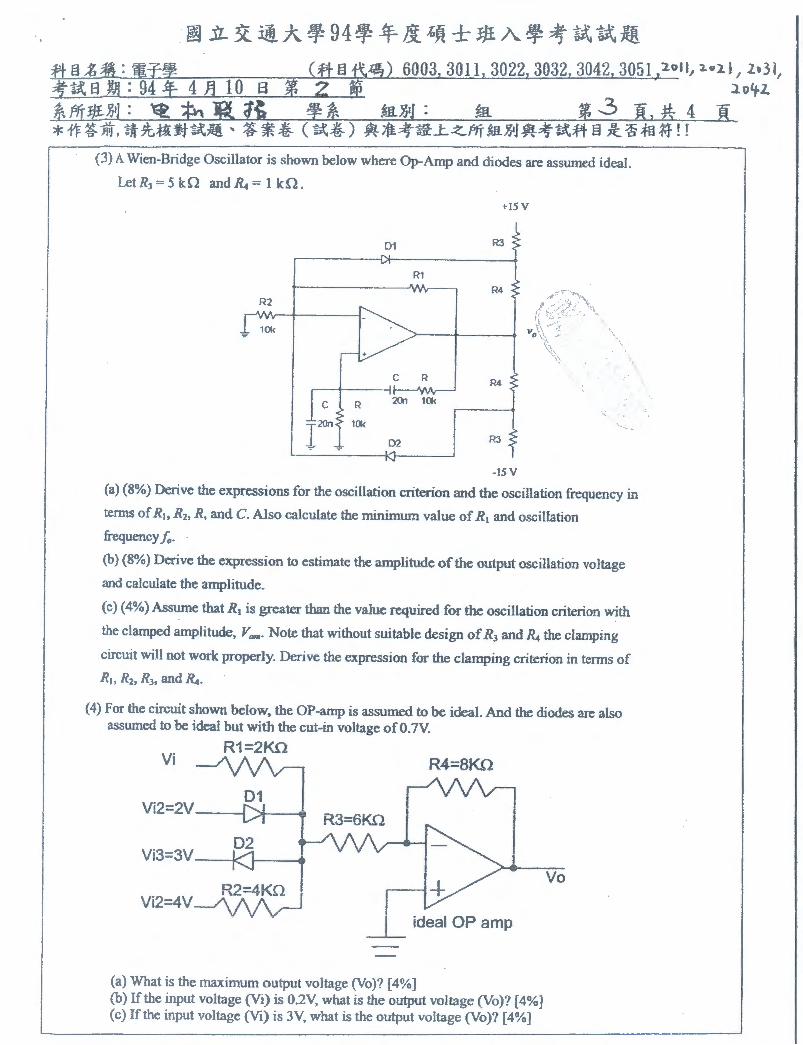
(3) A Wien-Bridge Oscillator is shown below where Op-Amp and diodes are assumed ideal.
LetR3 =5 kQ andR.= 1 kQ.
+15V
01 R3
Rl
R4 R2 1'>1' •.•• "-.\\
."1~ .•
!i
10k
R4
-15V
(a) (8%) Derive the expressions for the oscillation criterion and the oscillation frequency in
terms of R" R2, R, and C. Also calculate the minimum value of R 1 and oscillation
frequency fo.
(b) (8%) Derive the expression to estimate the amplitude of the output oscillation voltage
and calculate the amplitude.
(c) (4%) Assume that R 1 is greater than the value required for the oscillation criterion with
the clamped amplitude, V ..,.. Note that without suitable design of R3 and R4 the clamping
circuit will not work properly. Derive the expression for the clamping criterion in tenns of
R., R2, R3, and R..
(4) For the circuit shown below, the OP-amp is assumed to be ideal. And the diodes are also assumed to be ideal but with the cut-in voltage of0.7V.
R1=2Kn Vi ~ R4=8K.n
01 Vi2=2V __ _, ~J...---@
Vi2=4V _j_ ideal OP amp
(a) What is the maximum output voltage (Vo)? [4%] (b) If the input voltage (Vi) is 0.2V, what is the output voltage (Vo)? (4%] (c) If the input voltage (Vi) is 3V, what is the output voltage (Vo)? [4%]
Vo

(5) In the following enhancement load amplifier, the two transistors are identical. V 00==5V
and V GG=2.5V. vi is a small-signal voltage source.
The measured transistor I-V characteristics are shown below,
Vos{Volts)
3
3
2
Vos(Volts)
3
4
4
los( rnA)
82.4
83.2
20.8
(a) Calculate the threshold voltage Vt and channel length modulation factor A of the
transistor. (6%)
(b) What are the output resistance and the small-signal voltage gain Av==vJvi of the
amplifier? (9%)
(6) In a given CMOS process, assume the propagation delay of a specified inverter is 11101
nano-second under the supply voltage V 00 of 3V. This specified inverter has an input
capacitance ofO.lpF and an output capacitance of0.3pF.
(a) What is the output frequency of the ring oscillator that is formed by such specified
inverters with 101 stages in cascade? (5%) (b) Neglecting the short-circuit cu."Tent, what is t.i-}.e averaged power consumption of the
ring oscillator that is formed by such specified iuv~~ v.'it.ltlOl st.ages in cascade? (5%)
(&~t~Jiff~95- 1 ···· ·· ···· ·· · ·· ·········-· ···· ·- -··· ····· ····· ····· ···· ·· ····· · ·· ··- ····· ·· ······· ··· ·· ···· ---··· --- ·-····· ··· ···· .. ······ ···· ·············· ·········· ·•· ·· ··· .. ·· ·· ··· ··············"''''''' ' ' ' '
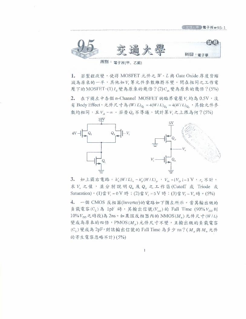
---'L,:.Immm ~~!smmm ~~m~T:J ?Jil.l~ : ~~PJT(Efl, Z*Il)
1. *~;f£~k~ '1Jt.1."t- MOSFET it1f-_z_ W, L ~Gate Oxide Jl-)j_ 1§-f,ffi
~~~*~-~,~~~~*it#~--#~~ o M~~~_z_~~t ~T~ MOSFET,(l)Id tf_~~ *~ ~1%? (2)Cgs ~~~ *~ ~1%? (5%)
2. ~ T ~ iL t ~11§J n-Channel MOSFET ~ ~ $ t ~ V1 JS] ~ 0.5V ' ~g_
:1f Body Effect' it1f- JZ. -t ~(WI L)Q1
= 4(W IL)Q2
= 4(W I L)Q3
' ~-M;it1f- .$-
i 13S];fl:1 ~ ' JL VA= ro 0 *-I- Q3 ~~±a ' t~tt ~vi -Z__l_~lt~1"J? (5%) lOV
5V
' 4V~
,c I.
.\ ... \.' ...
3. -;ko_l_~;Gt~ o k;,(WIL) " = 17-~(WIL)p 'V,n = IVtp 1= 1 V' ro ~ tt o -'K Vo _z_ 11 ' .3t f1- Ji1l tJt SA Q" E.. Q p _z_ ~ 11 ~(Cutoff ~ Triode ~
Saturation) o (I)'&" Vi = OV a-t; (2)'&-Vi = 5V a-t; (3)'&-Vi =Voai- o (5%)
4. -100 CMOS &.i!:l ~(Inverter)~'ltt~~T~iLF!f-F o '&-~.ti.Jtl:l flUlJ
~ iX. it Z- (CL) ~ lpF Bi- ' ~.ti.J tl:l1t ~ (VouJ ~ Fall Time (90% Vnn f 1]
10% Vnn _z_a-t.f~)~ 2ns o -;ko ;Jfd~&.i!:l ~ pq ~NMOS (M,.) it14- JZ. -t (WI L)
~*~~;f-.~ ~m1% ' PMOS (Mp ) it14- JZ. -t ~ ~ ' JL.ti.J tl:l f.&.~~ iX. it Z. (CL) fit fiX.~ 2pF' ~Jjt~-f;f,j tl:l1t~flJ Fall Time~% ~y ns? ( Mp ~ Mn it1f
a9 '* .1.. t z..~,~~ tt) (5%)

.. ?!5..~~-~~ .. §.!t~~t.~~~@#~~ .................................................................. ................ .............................................. .
VDD
rl:I ,:·~" V._j ~V""' :
I . ~ 1 2 sv ----------+-- -y c '' M T I. i i . ' '
' ' ~----+-+-4===~~ GND OV 3V 3.5V 4V 5V
5V
v,
OV
5. E. 9;o - 100 CMOS &.. ;f§ 5 &.. ;f§ 5 (Inverter) ff-1 Voltage Transfer
Characteristic *0 ..l.. ~ ii .PIT iG 0 ro, J:!:.&.;f§ 5 ff-1 Noise Margins (1) NM H ' ~
(2) NML ~~ !P y? (5%)
6. ~ r &i] .P!TiG '1f liB100 ~~(~a~~ b);f~ -k jfJJi CMOS Logic .z..NOR
Gate, J:c~100~~ff.J7(Af-JZ-t(DeviceSize)'*';f§~ oro, (5%)
(1) ·~-100 ~~-t":il:if& Body Effect ff.Jt.J~? (2) Body Effect -t"ftil:c
NOR Gate .Z.. tPHL .tkl& 1t Jf t.J ~ ? (Pg /}fl , /F ~ , ~-ki~Y )(3) Body
Effect -t"ft Jl:c NOR Gate .Z.. t PLH .tkl& 1t }j, t,J ~ ? (J'.!t /]fJ ' /F ~ ' ~ -ki~ y)
• ..
'\.1 ,.., ...
(~a) CliMb)
7. ~ r ~ .P!TiG o ~ (a)-Z...&.. foJ 511 ;f§ ~a~ ..l..-Jt a~ M (Rise Time)~ T Jlfat M(Fall Time) o ~(b)-k-100ft.Ji%i!ff~~' iiTJJiM1 ~M2 .Z..7iAf-JZ -t;f§
~ o tt t~ J±: M 1 ~ M 2 -Z... (WI L) 1R.. #- ~ (b).Z.. 3f! ~ ~ ~ 1f ;f§ ~ ff.J *ft. 2

...... .. .................................................... .............................................................................. ~~-~f.!..~-~-9..?.~} ..
(Worst-Case)J:_ ft-Bi- M ~;l!:. T Ff-Bi- M o (5%) VDIJ
15/1
B--1
v, V. A --1 8/1
(a) (b)
8. -_ko J..:l. T it ~ IE i£ f'fT 7r- o 1~1 i'~ Ql it a8a ft. fA VBE(on) = 0. 7 V J..:l. .&.
fJ = I c 1 I B = 9 o tt tx t1:: vo Ef.J it~ it o $ ~ Ef.J ~ 1:. it jJi: + ~ 1om v o
2mA
21ill
lkD
9. J:.. ~ ;fJ rf C--+ 00 ° ~ s8afit-Z... VBE(on) = 0.7 V ' VCE(sat) = 0.2 V ' /3 =50 '
Them1al Voltage Vr = 25 m V o t~ J~ tl:: Jl:c 1Ji ;k ~ f!] '1, -m ~J}t it ~ :I:W ~ '
Au= V0
lui o (5%)
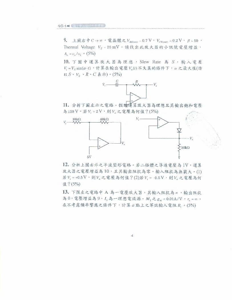
10. T ~ 'f .1! ~ 1Ji :k. H ,~ JJ. !l ' Slew Rate -~ S ' ~A 't l!f_
Vi =V5 sin(w·t) 'tt~4~tl:: itlM V0 (i)~3k_Jta011}14-T' w -Z...Jfl;k{it(tt ~;_ S, V5 , R , C *:iF) o (5%)
c R vi ---11---...-'V\J'v---....--- vo
+ 11. 7i-#r~iL:iF-Z...~~ 0 1~1tt"· ~ffi:.AitL~J£~JiJ't~tl::i8;fuit"-1j ±Io v o $-vi= 2 v , J!IJ vo _z_ ~~ ~10J11i? (5%)
'-------+---v;,
lOk.Q
5V
12. 7i-*IT J:..~;t-;;F_z_.f;ft!lff3~~ o $-..=..;f!i!fit-Z...iti! ~~~IV, .1!-J 4t:k H-Z... ~~:l:f ~il; 10 ' Ji}t~ tl:: F.ll.f!i:.~ $. ' ~ AF.ll.f!i:..i1 ~ ~ ;k o (1)
*vi = +0.5 v , 5!11 vo _z_ it~ .i110J 11i ? (2)$- vi = -o.s v , 5! 11 V0
_z_ ~1M ~1or
1i? (5%)
13. T~iL-Z...'%~4' A .i1-~~1Ji;k~ '}t~AF.ll.f!i:.~oo '~tl::F.ll.f!i:. ~ 0' it~:l:w~il; 9 ° II il;-.!J.~ ~ifiU..W. 0 Ml -Z...gm =O.OlA/V 'ro =00 °
.{±. /F ~ J.t ?JiJUf'. ~ J.i -Z... i\;} 14- T ' tt ~ a .~.5 J:.. -Z... ~ ti. ~A~ F.ll Ri o ( 5%)
4
.\

............................................................... ... .. .................. .. ... .. ........................... ~~-~:!.:m. ..... 9..?.~.? ..
Ia~
~I, R,
Vss
14. J:_ lli] ;5 't Iii-k -100 Common-Source Amplifier with Active Load o 't a8a H. Ml .&. 't ;)fiUlt. I I J!-:13 {EJ liD a1 Output Resistance ' ro 0 4'- vi ~ft ~Jt;)J,t ai] tf? t!:: F.li~Jl:.~ 0 ' 5!Jl Jl:I::.;QtA E 81 Transfer Function or~ J#.. : A (s) = V0 (s) = A M l + slmz
u ui(s ) l +s l mP
.5K(l) AM ; (2) mz ; (3) mp -Z_ /~ A 0 J.-:l-. g m ' ro ' c gs ' c gd :f<..7F 0 (5%) •
15. 1f -@J~;QtA E ~Tllil f'IT7G o %--It Loop Gain ILI = IA.BI » l ' ->R Jl:I::.;Qt;k.~-Z...'t~J:>gJ;aAuf =U0 1ui EJ10.:i( 0 £J.R1 'R2 'R3 'R4 'R5 'R6
:R7G o (5%) -·.,
R s
R,
__!_ - -
5
' '
., ' • ! 7 ~ .)
9 ?..~?-~~--~~~?!~1i!l~~~W!.~ ................................................................................................................................ .
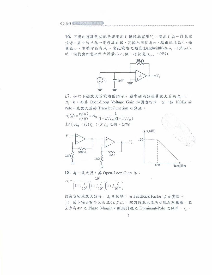
16. T IE .Z. 't 4-ft. :r.fJ fiE. 7~:Jl¥- 't ~fit I i ~ ;f~ 1.!; 't ~ Vo o 't ~i'fd; ~ - J.! !l 't ~~oiE~~A~-t~&AS'-ft-~Am~~oo'~ilim~~O'~
Jt~oo ''%~:!:'3~1.l;Av o 'tJi:C.'%4-Z.:!J;~J[(Bandwidth)~m8 =10 9 rad/s Bi- ' tt:A ill fJT ',W; .Z.&;k ~ ~ + Av {itt ' ~;?JL.R, Au min ° (5%)
10kn
17. :ko r;. T ~&A B 't41E fiT 7F o IE ~ ~ ~100.1!Jt.&A B ~ R; = oo • Ro = o ' rriJ -ft. Open-Loop Voltage Gain :ko IE .:6 fiT 7F ' 1f -100 1 OOI-Iz siJ Pole o Ji:C.&A S ~ Transfer Function Of~ 1#. : A(f)=vo(jf)=A 1
v J U;(jf) M (1+jff(p1 )(1+jff(p2)
-''R(l) AM ; (2) fp1 ; (3) fp2 .Z. {t o (5%)
A,(dB)
1201----,.
18. 1f -&A~ ' -ft. Open-Loop Gain 1.!; : 105
A = ----;-----c-;-----c:-:-------:-
" (1 + j -4)(1 + j ~)(1 + j ~) 10 10 101
100 freq(Hz)
1i * ~ @1 #'::Ot ;k ~ Bi- ' A" /F & ~ ' rriJ Feedback Factor fJ k jf it o
(1) %/F~fJ1f§AnnJLO=:;fJ::n '~@J;f~:&.;kS:!:~tif~~k./F.:MUi 'JL
_i_j'1f 45· .Z. Phase Margin o 5!1]11!31 !1!-Z. Dominant-Pole .Z.:!J;~~ ' fv •
6
............................................................................................................................................ ®H~~t;t._~i:!.!f._~_9..~-~.7 ..
~10J 11i(Hz) ? (2) £M(l) ' 1ET..~ 'fft; -t- Phase Margin ' f!r Phase Margin= o· o
tt .J:.J.. Piecewise Linear Z. Bode Plot .;t_M ' r.J.. r~ 1b tt 4 o
19. -ku 't ~ ~ fiT -;F o m ~ V; EIJ fif,J A tfL ~ , fif,J ill 't ~ or ~.J.. $:. ~ l-9 Vo = 3 + sin(2;rft) V o tt .:f~ ill 3.1 a:t Q1 't Jls ft )tf ~ EA if JS] :r-:/J $- ' PQ, o £A
mW ~1;-1ft o (5%)
5V
.,_
" '· ' ' , .. ~( r :·, .:)
20. -ku ~.J.. T 'tll!i! f!T-F o 11k -1~ JfJ &..:fEI E(Inverter)jJl~ EI-J.:f&j{_ E o liD ~k&.~BEI-J#tlo•aill~.:J.&j{,EEI-J.:f&~M$-o~o~lli~~~o
tk)i- ;t ' &..:fEI E EA tif.J AA'i'r; ~~~ /Ju J:..1£10J Clamping it li! ' jt.fif.J AY#6 Ef] 't ~or~ t1:: o~5v E~-J j[ oo o (5%)
7

.......... .................... .. ............................................. ........................... .. .. .... ... .......... ............. §A~~~~-~f.!.!i.~ .9..E5.-:. ~ ..
1. ;'t~;t 't$.Z..* fit~~ if~~ H(w)~oT ~ .iLf'lbT- '~k*~ ~i'f H(w) ~
~~tl:l? 2R
IH((JJ ) I (dB) R
. . ~· ' '· .
- 60dB/decade
2. ~o J:~J::_ 't$E ~ ' -!t- 'f EIJ ~100.1{$-:a*-(Operational Amplifier)~:£.!
tB 0 ;~-; it i!f ~ilK JBir ~ A = Vo 0 ~~ .,....J'.. / "' "'t:.. 1'1£. a .:on. v
~ 3. ~oJ:~T't$~£f'!TiG o Jt'f~.!f$.&*-~(Operationa1Amplifier)1f
fi\t,~ft.:k.~~A.~Ji{!i.. '~tl::lrli{!i..~ 0' iiTJ'tJ~U'f!l,;i~ 9 o -=-t~.ft(Diode)Jll~
foJ1~~(Forward Bias) Hi- ' Vo=0.7V o 1; Vi=2V Bi- ' tt~ tl:l V0 ~ 't~ o
5V
v.
v;-j

96-2 ~~ til"#£t'~.dW1Mi1fA» •••••••••••••• • • • •••• • ••••••••••• ••• •••••••• •••••• •• •••••••• •• ••• •• • •••••·•• ••• ••••• • ••• •• •••••••••••••••••••••••••••••••••••••••••• • •••••••••••••••••••••••••••••••••••••••••••••• • •••••••ooou••
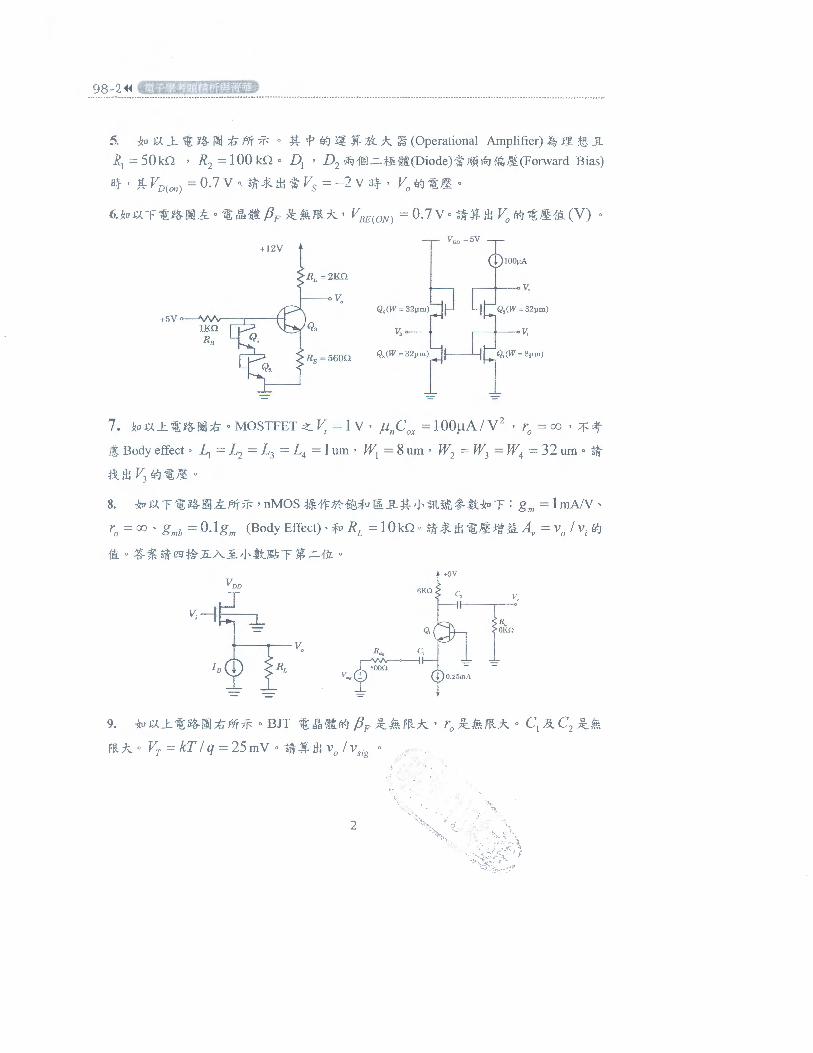
ifiJ Jl:C.3tAf- fiJ £*41-·11-k JLCoxCW) = 5 mA I V2 & Yt= l V o ~;JX tl:l Vi fiJ 'tl!f L
ifi11~A~- V0=2.5V o
5. :koJ-:J.T't~mJiL?!TiG o 1Kt9: BJT 2:.¥f.i!'t~ VsE=0.7V' fJ=oo'
-''R Vs 2:.Jl'k;k W-1~ BJT "Ti:>Yd'F~ forward active region ( VCE z 0.3 V) o ( $
~ 't ~1=l £ j.' -=-.11L1f 5<±-it ~)
n: 1 ~--~ ~--------~
v.
6. :ko __L mJ -:6 2:. Bridge Rectifier "T ffl J-:J. 1{ 1Jf-1i ~fit 't ~ #.] tl:l '1~1 't9: .::..t~ 'itt 2:..¥}.1!-t~~ 0.7V, RC>> lsec' #.]A't& Vi~ 60Hz, 110Ynns2:.xifit
't~, -'R~& ~ 2:.tt~ ~;C. n 1~#.] tl:l1i1~1t 't& Yo~ lOY o ( $ ~ 't ~1=l £
j' -=-.1il.1f ~it ~ )
7.
ro = oo ' V oo=2V ' #.]A i!t J!f ~ 0< Vi <V DD ~II] 0J ft. it ~fit i ~ 1f -Jl'k ;k
11 ipeak' %~1~ ipeakifo\+~~*-2:..114' ;Jt?!T't2:.. Yon i!t& o
V DD
\ .....
GND
8. -100 CMOS &.;fJ:J ~ (Inverter)a\1 't~:ko __L mJ -:6 ?IT iG , ;(f_ ;'t -;j~ Jt a1 CMOS tL;t£ T ' ft. Logic Threshold (Vth) t:.;flt't9:tt ;(f_ V oo/2 o
2
... ..................................................................................................................................... ~~-!f.!.!f.~.9..9..~} ..
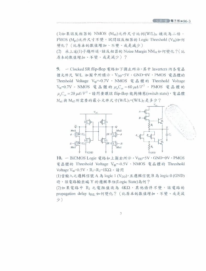
( 1 Ho *-~ .&.;f!'l ~ fi-J NMOS (Mnl) 7t 14 JZ -t ~t.17'1(W /L )N it ?5( 1.9 ..::..1% ' PMOS (Mp 1 )7t14JZ-t:.f~ o ~~M~.&.;f!'l~fi-J Logic Threshold (V 1h)~o1iiJ
~1t.? C ~t.~.t--fi-JttiRtw!Jcr, /F ff , ~kifi&jl')
(2) .if._J:_:i!_(l )-f-it! .PIT .i!' ~ .&.;f!'l ~ fi-J Noise Margin NM1-do 1iiJ ~ 1t. ? ( ~t.
~;f..fi-Jtt~~~-/Fff-~k*~)?
9. - Clocked SR flip-flop it ~~o TIll !L. .PIT 7G ' -1t 4' Inverters pq ~it a8s
M.7t14JZ W/L ~ &!] tf .PITt~iG o Voo=5V' GND=OV 'PMOS it s8s1ltfi-J
Threshold Voltage Vtp=-0.7V ' NMOS it Is 1lt fi-J Threshold Voltage
Vtn=0.7V 0 NMOS it Is 1Jt ffJ f-LnCox = 60 ,uA/V2
' PMOS it s8s ·Jtll ffJ
f-l pcox = 20 ,uA I V 2 o tt r,, -t:-tl ~ flip-flop 1J5~{;; ~ M (switch state) , itt Is 1lt
Mn, ~ Mn2 PIT 1#; -1- fi-J J!l,J, Jt14 JZ -t(W/L),=(W/L)2 k} j' ?
10. - BiCMOS Logic itt~~oJ:..IIJ.E.PITiG 'Voo=5V' GND=OV 'PMOS
't Ia -H. fi-J Threshold Voltage V tp=-0.5V ' NMOS it s8s 1lt fi-J Threshold
Voltage Vtn=0.5V ' R1 =R2= lKD o tt M
(1)~ #:) A~3i.f!f-1t Mt, A 1.9 logic 1 (V oo)' li3i.f!f-1t ~t B 1.9 logic 0 (GND)
s-t ' tt itt~#:! ill Mit, Y fi-J 1i.f!f-i1-1.IL(Logic State)i.91'PJ?
(2)~ *-it~ tf R2 ~itt ~Ji-lt ?.t i9 4KD ' $ ~1;}14 /F ff ' tt it~ fi-J propagation delay tPHL~o1UJff1t.? ( ~t.~;f..fi-JitiRtw!Jcr '/F ~ ' ~k1A
~)
3

11. ~t~r't~~?JfiG o 1~1.-t~ VsE=0.7V' fJ=oo ' kT =25mV' ¥+ q
v 1fl~t:t£J'3 ~ Av =; o
I
+15V
lOOkQ
~~ v~ ---
= lOOkQ
12. ~{Jfr~E..:t.JE1/Jtf't~ o ;¥: MI ,2,3,4 .:t.~~{i(Transconductance)
~§'~ lmAN, JLJ't.tf.Jt!Hll{li:.ra ~~fiR.MA o R1=R2=Rs=lOKQ o ti\ .. ,-~.jt.
1~:JY~+1t~JE1/J't£~~Adm =(Vo+-Vok+-V;-) o (:1f3ttit~ 31ft)
R,
13. ~{Jf J:.~ i1 .:t.lE1/J 1f't~ o ;¥: M 1,2,3,4 .:t.~~{i(Transconductance)
I§'~ lmAN ' JL.jt.tf.J ill ~ll{!i:. r0 I§'~ fiR. M A o R1=R2=Rs=lOKQ o t;\.;R_Jt.
1d- Jlol'i J 1~ .!!.!;> .:!±.. _p+ .;'W Tfi: Jiil ~ A - V oc~ J:t ,-h V *- !A ill 1~ ~b -->? .:1±.. -!_,_,_ .;'W ~"~~ 1 '·15 ~iL ,, -1~ ~ 1::£:.. a :Dn- em - V ,., , T ocm_ q -'ffl1 iLt -Iii JJiL..<._ ,, 'T~ ~ ICm
Jl ' Vicm ~tf.J A 11: ~.:t.#{~ 't Jl: o ( :1f 3itJ!t :f 3 1ft) 14. ~{Jfr ~E..:t. 't!l:&A~ o ;¥: M1 ~ M2 .:t.~~{i(transconductance)
4

€f~'D11::r-Pfi .. 96-5 ·--~-··························-······· •••• ·····················-···· •••••••••••••••• • •••••••••••••••• - ~ --- •• ••••••••••••• •••••••••••• ••• •••• 40000 •••••••••••••••••••••••••••••• • ••••••••• • ••••• • •
~ ll; lmA/V ' ll~~ tl:l ~lL;J!i:.r0 1r 1!.;~~ A o Cgs=lOpF ' Cgd=2pF o t~_,~
i[~pg ~ A(s) = (Vo+- Vok+ _ V;-) -Z...$-.~(fz)~t~~.!;~~ ;f.(fp) o ( JF-1ft :
lli·~~-~3~·A~tt$-~~~~k~~~-~~_z_~~~~~ VDD
iJ~-'f~)
c
,: I'
-~· ' ...
v, --l
R,
15. 1};fff_t_~;t--Z...it~ o *" M1 ~ M2 -Z...ff¥}-ta(transco ductance)1r,ll;
lmA/V' ll~-t;fu-tl:l~li{!i:.ro 1rl.!.;~~A. o Ri=lOKQ 'Rs=lKQ 'C=lpF o
v t~_,~Jl:c it~.z...1~~+1t~ it~~~ , ____£_ o c :1f~±•~ 31ft)
V; 16. 0-;fffT ~ ~-Z... it~ o *" M 1 ~ M2 -Z...~ ¥}-Ul.(transconductance) ~~ ib lmAN' JLft--t;fu-tl:l~li{!i:.r0 1rl.!.;~~A. o Ri=lOKQ 'Rs=lKQ' C=lpF o
v t~_,~Jl:c it~.z...+1t~~ ~ , ____£_ .z...-3dB ~~ Jt o c ~ ~±•~ 31ft)
V;
R,
5

17. ~;f!f J:_li];fJ.Z.. ~~ 0 ~~~;k~.Z..+1t~t:t~J'Jf~~ 1000' iff]_]_
::1i~100t!i!.W.5 '~JU¥~Ji'l~ fpt ~ fp2' Jt<f fp1=lMHz' Ji.
f p2> > f p 1 o 1{ ~ ~ ;k ~ .Z..tfu-A ~il{Ji:. ~ $.¥; ~ ;k ' iff] tfu- tf:: ~il{Ji:. ~ $ ' fp 1 fot f
p2 .Z..~~ $-~ x @J#:~~~_z_;f_;~ o ;¥:-t-T li] ~~.Z..;ff:l1Jti!$(Phase Margin)
4 60°' ti:.:,-j(_ fp2 .Z..~~$ii o ( JP--1ft: Hz' ~~ilk+ 31ft)
18. ~ ;f!f T IE li. .z.. ~ ~ o _:¥: Mt,2,3 ~ .ti 11 :¥--if!, ;fu !& ' Ji. ~ ¥f m (Transconductance)~~ lmAN ' Jt1t-.z..tfu- t1:: ~il;J;t r 0 ~ ~ $.¥; ~ ;k o ti:.-R
v Jt-1~&~~+1tWL ~~:tw ~; o
I
"·
5V
···--it· "· 1oon
:]V
t•,~lV
. \ :(
' '
-.,
·· .. ..
19. ~u ):...( J:_ ~ ~ lil t1 ?IT 7G 0 w :¥-- vi tJ:J A 1ft. We. a~ {if J;IJ ' v 0 ~ tl:: 1ft. ~Lt k-100-it. 1 V .&. 3V .z_ M ;Jijt:tiJ a~ 50% Duty Cycle ~JiJl ·t± 7f ilt , ~~ $ ~ 1kHz ,
:J(u IE o tt t~ tl:: .1! B:f M 1 it Ia It ~ti :f-t ~ f Jsp.fJ $- ' PM 1 o .1-J.. m W ~ JP--1ft o
20. ~u;:...(Ti!t~lil.P!T7f- o Jt<f R=lOkD~C=lOpF o ~a8aH'..Z..g111 ~;f§
~·iffJJi.~~4Jt~7t#*iko#~~;k~·~~~·~-o-aili
ifdi~~$-fosc o ):...(Hz ~JP--1ft '$~~Y-t-~ 31ft~~ilkef o
6
.......................................................................................................................................... ~.!!:!.!!..~~.9..?..::-.! ..
ffi8~ : ~f- PJT
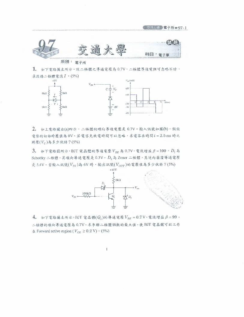
1. -!toT't~~£.f!T7G • 1& . ...::..;f.~'At.:t.ifi!! 'tiM.~ 0.7V' ...::..;f.~ 'At ifi!! itfli or .~-~/Ftt '
;Ji.J"~t:i&...::..;f.Ht'ti"~tl o (5%) +9V
Bkn I 3kn -- v +
5f t(ms)
3kn 6kQ
-BV ---------------·----
= -
2. -{to.l..'t~~;G(a)fiT:;F '...::..t~fitf/.JJ'I~foJifi!!it£k 0.7V o ~A.tfl3it~o~(b) • 1~Hi
it Z.a':J:fJJM;Ift£1Ri9 ov o * 1: Z.Jf.;JP:.. 't a;t M or.~-:;,.~-~ · ¥it Z--1£.8;} M t = 2.5 ms a;t.:t.
~£(Vc ):1.9 >f }'11-di-? (5%)
3. ~oT 't~~f!T;;F 'BJT 1: Jla:lltf/.J ifi!! it£ VEE~ 0.7V' 'ti"~t;f;>g ~ ,B = 100 o D 1 lJ,
Schottky ...::..;f.}. fit' $,-J'I~ foJ ~i!!. 't£k 0.3V o D 2 ~Zener ...::..;f.}. :lit' .ft:iifoJ iffl ~f¥}1!! it£
7t_ 5.4V o 't ~ A.tf1.3t( VIN )is 6V a;} ' ~ tl:l-m. 3t( V0 ur )a':] it£ 1R~ >f Y 11di- ? (5%) +lOV
2lill
''·.i
4. -!toT it~~ £.f!f7G 'BJT it a~ :lit( Q1 )fi-J ¥}1!! it£ VEE = 0. 7 V' it )~t:!:'N ~ ,B = 99 o
...::..;f~ :lit f/.J Jil~ foJ if i!! it£~ 0. 7V o ..;R * ll~ ...::..;f~ 'At 100 it a':] lit A 1R • 1~ BJT it Jla :lit Of.~-:;, .:r..1t
1±. Forward active region (VeE ~ 0.2 V) o (5%)
97-2 ~ A4il.tJdML'}11i'flt oOOOOOo o•o ••"'''•oO UO OO < O O OO Ooo oooo ooooo oo OOOooooOooHH000<000000<0<000000.oo o ooooooooooooooo o oOoo~oo oo ooooo oooo o .. o oo o 0 000 0000000# 00o OOOOH Oo 00 00 0 000 00 00#00#0000 0 00o000•0 0 0••00o ooo ooOOo O O O UOo
5 . .j(o_l:_'t~~;;GfiT:;F' ~100 BJT 'ilta8a:llti§".:r..1"f-ff.£~l&(Forwardactiveregion)' 1Fi
t9:.:Jt~i!'ilt£1 VBE I~~ 0.7V' fl~{t(Transconductance) gm ~~ lO(mAN)o 'tifrt~~
fJ ~~ 4, ~tl:: 'tr.liro ~~oo o ;R+-m.~'i[£:J:>g.M.Av =Vout /vin o (5%)
6 . .j(oTi[~Jm)J:.JS!f:;F • BJT il!:a8a..ttfi-J~i!i!t£V8£ =0.7V • 'tiF,tJ':~/]=100'
f;jj tl:: 't r.li ro = 00 ° ~l-i..:i iRt ~~ i!1: ifrt I Cl = 5 mA ' 1& 't ~A iRtltl-i. 'ilt £(VB) i:.1t BJT
1: J'a:llt.:L1"f-ff_ Forward active region o .;J<..+tft.~~A 'il!: ~.li (R;J o -fri~ kT I q = 25 mV o
(~&~A-~~~~~~·*)0~
+9V
15
7. .j(o J:_ 't ~ &iJ .:6 Pff :;F : (1 0%)
(1) 1fi~ Q1 ~# ~Pb~1t(gm)~ lrnAN' ;R~A'tr.liRin o (5%)
(2) %' VDD = 5 V • NMOS ~k~(W I L) = 0.2mAN2 • Vt = 1 V • r0 = oo o 't 1; ~h'a" · "' · ··
fl) ~-~.k+ at • Q ~\}:i!A triode region • ;RJl:cBt~ Vo o (5%)
2

....................................................................................................................................... ~~~-~:!:!!. .~ ... 9..?..~;3.
(I) ~t differential-mode
(V0'- V
0- )I(V/- vi- ) o (5%)
(2) ~t common-mode it ~ :l:W ~ (Vocm I Vicm) o
VOCnt : ~ill common-mode i!t ~ ; vicm : ~A
common-mode it~ o (5%)
20KQ 20KQ
120KQ
9. ~mm~•~*s•&~~T~~~-4:~~-~~c~~. ~. ~·&~ ~:;Fi:_)o(5o/o)
c
10. -)(oJ:..'t400iJ?if:;F • 111-t~~~~ABi.bJ!.~. • t~ttR1 • Rz • &Cm • 1t~AB
't 411-% .~-:;,. T fflA% : ~A fllttL 1 KD · DC 't ~ :J:iW ~ 20dB • l- - :l:W ~ (unity-gain WJ;t Jt lJ; I 000 rad/sec o ( R 1 • R2 • lit C 11i ~i't ;f tt 0'-) (5%)
11. -)(oT IE~~AB 't4 · R 1 I R 2 = 9 o %-~l.~A B i:. 't~:l:W ~(A) 1.9~ f!U.t · t."\
3kD
3
.. -.. .
'~\~,..,_I f~ ',,_!,
97- 4~~ Gt;ifi&iridMmlttiii) .......... ~-. ............. ····-·······-·········· ············ ······-····· -··-··-- ·-· ···-· ·-·-· ................... ···-·-···· ......... ········---~---- .................. --··· ....... ····- .... ·····
A'i!t/2t vi tiij ov o 1t vi ~ ov ~-Jt ~ 6V a:f , tl::.a:f~ ill 't/2t vo ij1;;y? (5%)
13. l-:J.l.f~-~J}ffi:.}d~4:lt-*-:koT~li...W.Ji:~'t4, R=l KQ, L=JmH, .,f_.ft-.W.Ji:%J-!iji_
!f- aJ (rad/sec) o (5%)
14. 7i-t!f 1-:J.J::. liD ;;5 't4 o ;6-ffi:..:k. ~(G) .Zftt,11!!4Jib ~ A 0 = 103 , llft- ~3i'Jiz -3 dB 3l>!i:
v J[.(aJ _3d8 ) ~ 108 rad/sec o ~*- Vo z (l)1~3i'Ji -3 dB ~Ji!fs.' aJL (rad/sec)(5%); (2)~-!iji_
s
-3 dB ~!i: !fs. , aJu (rad/sec) (5%) ; (3) 4' ~!i:~W ~(5%) o
15. 7i-i!fTigjli..z't~ o ;6-p!j-~ MOSFET ~1fH'f-{dg;fof&, ft-#~;t\W~(g".) ~~
lOmAN , R1 + R2 = lOOkQ , R 3 = 2MQ , C1 = 0.5 pF, C2 = 100 pF ll.ft-;fEJ1ir.:i!~
(phase margin)~ 45· o %- .~-~.7t1t-z~ ill El'I.t!L (r0
) '
(1) ;-~~J:.:?•J11},1t- , R1 ;W; ~ § j'? (5%)
(2) if<__Lfl!' Ji:I::.B:fz1MJi~ill~.!it!LR0 i\\;§j' ?(5%)
~ - -
' ,; . ' ~- '- ""~
V,-j
4

fll;ltl tltlt8 JRlBJI!fiHijf-, lltl. 11-=f. 11~. 11~. J'tll. IH!1l!*a. I!J.::bt!ltlit. HIPJT~98-1 •'" ' ••• ••••••••••••••••••••••••••••••••••••••·••••••••••••••••••••••••••••••••••••••••••••••••••••••••••••••••••• • ••••••• • •• • ••••••• • •••• • • •••• •••••••••• • ••••••o•ooOuooo•••••••-'••••••••••••·••
~~ ~ ~~~! ~.~m~t::J fngtl : ~:*:!t«IIJI!liHijf-f-UHJT ( Z:*H). ~liPJT ( 11-T. ~~ill). X.:*:
~-rm < ftl. z:~ ~ ~rim< z:. ~m ~ ~~m ( z:~ ~ 5!* ~~ffi(~. Z:.~.Tm~*~PJT.t-Tffi.IW~*~~~ PJT ( Ttdl ). tii.Jli~PJT ( Z:ifi ). ~IIJIIIIPJT ( II!J'Crill )
1. :tt -1m ~;f.}.·~i:fi Wi it 888 -u:(BJT) ' ~I c ~I 8 7i- liHz :iF~ ;f.}.(Collector)it ;1,t~£+~
(Base)i[;1,t ' ~ r,, T 71l·JJJI~ ~{{ i.'.t ~ ar pg jja it ;1,t:Vg ~ (,8 =I c I I B) :
(A) JWJ'Jat-J-;f.}.(Emitter)fi-J$'jf~$51t&; (B)i~Y£-f§.fi-JMi.Jf~Mt-5.!&;
(C) JiWJ'Ja~;f.}.fi-JMi.Jf-i~Mt-5-t&Nc ; (D)i~jt·£_;t.}.fl-]j[li_ o .:fii! o
2. ~T~£.fi-JiiP~'f, vsig~-_iEjt;,t+-m.~JL-f-J.~-(t~~ o 1~H~'tJa#A*1"F~i
ftJ !&(Active region) ' t-k r .. j T 71]·JJJI~ i.'.t ~ i'-1?.A!f- 't J~Uw ~ v 0 I v Slg Ph jja :
(A)i~+ Rs,g (B)pgJ'Ja Rc (C)P,t 7'Ja RL (D)i~+ RE :fli! o
+l5V
Rc v3 2R R
v2 vo
v,
' - 15V
3. ~a J.:_ ~ .:6 't lit ' Jt 'f fi-J ~~M:. 7dHOperational Amplifier)~ J1'. !'-!} o 4- ~ = 2 V '
V2 = 2 V, V3 = 4 V o *-ft-~lli 't~ V0
(V) o
4. ~" -"J. T &il £..PIT :iF ~ 1.h1t it ~ ' 1~H9:. ..:::-;f..}.1Jt ~ ¥?- i! ilt ~ il, 0. 7V , ..::::.- ;f.}.1Jt ¥} i! 't Jlli ~
0 o %-f;l1A 'tiL?. V; il,~~$ 60Hz· #di 4V ~5Ufit it~ , ~t-ilt~ V0 (V) o ·
R,
5. -Y,u f). J::_ i!t ~ li ii fiT ~ o .ft- 4' {I] if .J} ffi:. A ~ (Operational Amplifier) P.a l!. ~- Jl
R1 =50 kD , R2 = 100 kD o D1 , D2 Ff,;J1~ -=-~-mt(Diode)i;' J11f'! foJ1,%~(Forward Bias)
Bt ' Jt VD(on) = 0.7 Y o tt ~f- t!:l '&' Vs = -2 V Bi- ' V 0 {I] 't~ o
6.-:ituJ-:.Z T't~!Eil£ 0 it a8a1tit fJF k#.t-ffl..:k, VBE(ON) = 0.7 Vo tt.J} ill v" fi:J'tll-ii (V) 0
+12V
7. -Y.ofJ.J::.i!t~~ii oMOSTFETzV: =lY, JlnCox =100~LA/V 2 , r0
=oo, ;;r:,;lj
J.t Body effect o ~ = L2 = L3 = L4 = 1 urn , ~ = 8 urn , W2 = W3 = W4 = 3 2 urn o tt
.t~ ill V3 fiJ it~ o
8. -Y.u fJ. T i!t~li£F1f~, nMOS .tf/<1-f;Y:-~fu QL!i..ft-+tMt.$-tHuT: gm = 1 mAIV,
ro = 00 ' gmb = O.lgm (Body Effect)' fuRL = 10 kQ 0 tt ~t-ill i!t~.J:w j,i A. = vo IV; ff.J
11 o ~ ~ tt 1!9 #-li. A .f_ +it.~ T ~ .::..1iL o
+DV
Voo
V;-j
vo RL
- -
9. -Y.u 1-:.ZJ::. i!t~li ii fiT~ o BJT i!t s8s1tit {I] fJF k#.t- fltA ' ro k~ flt:k o C1 &. C2 Jtf¥1,
f!t;k_o Vr=kT/q=25rnVotf~illv0 /Vsig o
2
~-:Z ~BJHTiH!iV.f-, 71~, ~-1'-, itrl, t~, ;/611, I~~UU7L !bil-~, UIPJT~98-3 .. ~-.......................... ·······-··········· ···-·-······· ·· ··-··. ·····------~---···. --- ........... ····· ····· ........................... -........ ·-·····-·· .. ····-·-·-···· ···--· ··-··· ........ .
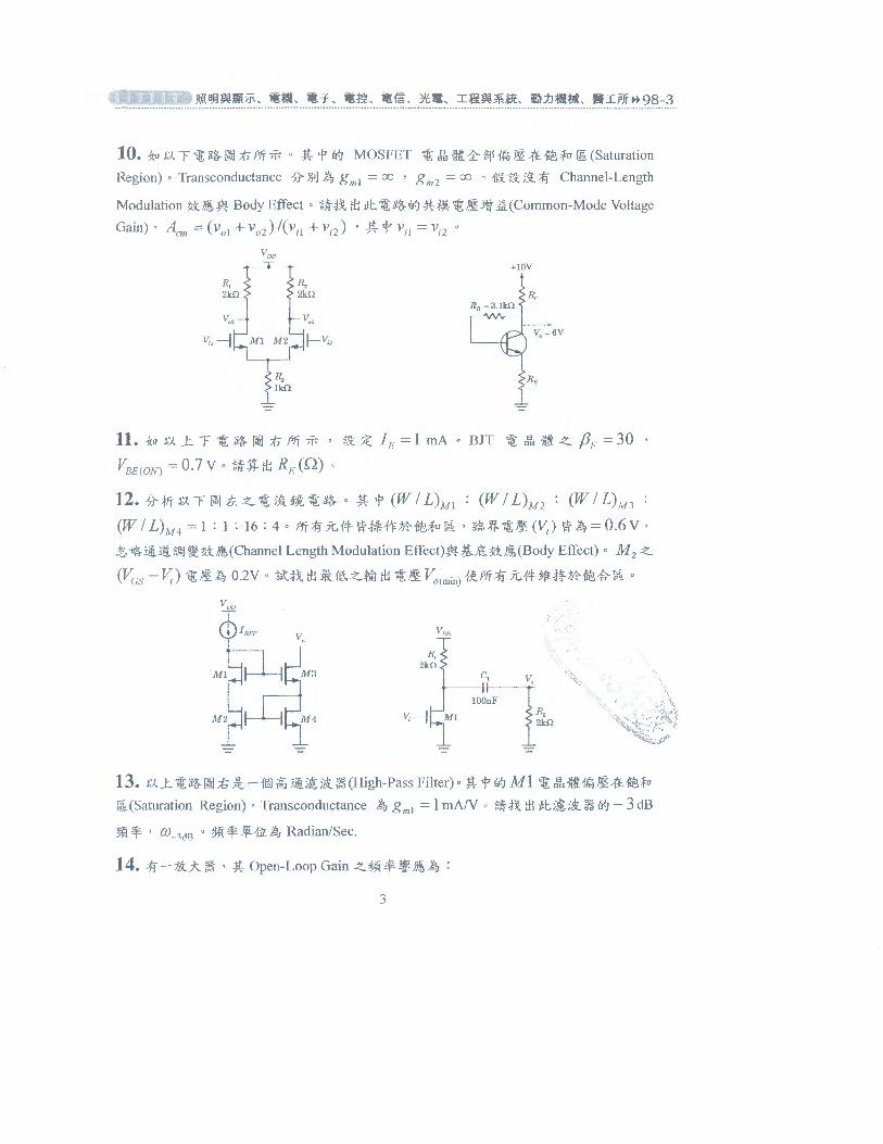
10. -l;,o ,~:;_Tit iifr 00 ;(:]fiT 7G o ~ 'f {(.] MOSFET it .!"a -tt 1::- -1}~ {~ lJI 1£ ~:fo !& (Saturation
Region) o Transconductance ~Jj1] :!q g 1111 = oo ' gm 2 = oo o 1R"t)t&1f Channel-Length
Modulation ~X. ft.!~ Body Effect o t}ft)(. tl:l.J:l:. itiifr€8 #{~it /t:!tW ~(Common-Mode Voltage
Gain), Acm =(val +vo2)1(v;l +v;2), ~'fv;J =vi2 o
R, 21ill
=
R, lkn
R, 21ill
+!OV
=
11. -i;,o r;_ _t_ T it 1ifr 00 ;(:]fiT 7G ' "t~ Jt 1 E = 1 rnA o BJT it J'a -tt .:t.. fJF = 30 '
V8EcoN) = 0.7v o ttJi:.tl:l RE(Q.) o
12. ~tiT j.), T 00£. .:t_ it )Jit i.t it iifr 0 ~ <f (WI L)M! : (WI L)M2 : (WI L)M3 :
(WI L)M 4 =I : 1 : 16 : 4 o f!T;ff Jt14 '§='~;f-1tt:'-~"fo I& , !IJi,~it/t (~) '§=' :tq = 0.6 V ,
.t:-~~.1!tfoli2t~ft.!(Channel Length Modulation Effect)~£.M.S<±fi.!(Body Effect) o M 2 .Z..
Wcs- ~) it/tjq 0.2V 0 t~#. tl:l :/&1l3..:t..ffi tl:l it& vo(min) HU!T1f Jt1Ht£~~t:'-~%~ 0
= = =
13. f),_t_ itiifrOO ;(:];it -1~ ~ [email protected] ~(High-Pass Filter) o ~ 'f {(.] Ml it .l"a~1~~1±. ~f'o I& (Saturation Region) ' Transconductance :!q g ml = 1 mA!V o t}fJ~ tl:l .J:b! ili ~ a0- 3 dB
:im$ ' UJ_3dB o JJ;Ji:$-'{trlq Radian/Sec.
14.;ff-:&A~ '~Open-LoopGain.:t..JJ;Ji:.:flJ¥ft.!lq:
3

A" =( X IO' .)( ) ·JC'l'!+Ud!\$(Hz)•lt>&~Sft~All 1+;·~ l+j-~ 1+;·~
1 05 . 1 06 10 7
Bi-• ~ ~ ~k~' iffJ Feedback Factor j3 > 0 :it. if it o 4<. j31ti.HifBi-• ~tmftffi:.fd~ ;1f 45'
~Phase Margin o .$. ~ .;b ~ k -:ko r;, T E01f3 i( : jJ = 1.234 X 10⁻² '
15. -:ko T 't 4 ~£FIT 7G o ~ <f E8 .1! .1} ffi:. :f:... ~ ~ ft_ 1JJ ~A. f.H. .f!L (Differential Input
lmpedance)i.l; 1 OOkQ '~ tl:l f.H..fiL~ OQ' iffJ JL.ft. f~t, 4ft- 1JJ 'tJ~V't .tl(Open-Loop Differential
Gain)i.l; 10 o ~ R1 = R2 =50 kQ ' -'R-ft llt,i@4(close-1oop)'t£.J:W .11 Av = v0 I Vs o
~~ -=rct----wv---+- 1 ·" I lOOiill
R,. '------1
16. -0-;f!fJ.:Z...l[Wi];6'~ffi:.:f:...~ilt4 o %-J'tf;1f MOSFET 1,Hf-+'F~~;foQk 'n¥?:t't.111ti.l;
g 1111 = g 1112 = 1 mAIV o ~;:if ;.t Channel-Length Modulation :0:.J.11!, o ~~I>:Rffi:.:f:... ~ ~~ Af_g_
;/!L ' Rin (Q) o
17. -:ko J.:Z T 't 4 ~ £PIT 7G o ~ <f E8 MOSFET 't Ia ~ ~ .g~ ~ £ 1±. 1fg ;fa Qk (Saturation
Region) o Transconductance -51- J}l] i.l; g 1111 = 2 rnA IV • g 1112 = 2 rnA IV •
g 111 3 = 1 mAN • g"' 4 = 2 rnA IV o 1R~&.;1r Channel-Length Modulation ~{.J.11!,~ Body
Effect o ~w ~ tl:l 11:1:. it 4 ft-J ft_ 1h it £ .l:W .11 (Differential-Mode Voltage Gain) •
VDJJ
Vo
vB-j
v,-j R2 1H2
_L _L - -
4
~
' '· ~ .~

(!lililil il le @BJJ~m;r-, ••• ~-f-. -~- 11~, %11, If¥~.¥t7t, ll!JJ:d~, RIPJf~98-5 oo•Oooo•oooOooOoOOoooooooooOooooOO•ooooooOOooooooooo00000''000ooooooooooooooooOOoO•OOOOOoOoOoooOoooooooooooooo'-OoooooOOOOoOoOoOOoo•OO•OOOOOOoooooOooooooo O ooH .. OooOoOOOoooooOoOooooooOOOO•oooo O o
18 . .j(a .r;, __!:_ i!t ~ ~ ;;6" PIT 7G o Jt t a9 MOSFET i!t .!'a 1l:lt ~ ~~ 1~ /!f: 4 ~ ;;fo r& (Saturation
Region) o Transconductance 1t Ji•l 1.!; g 1111 = 1 rnA IV ' g 1112 = 1 rnA IV o 111 "t~ & ;1f
Channel-Length Modulation 5&.fi.11 ~ Body Effect o ~it n tl:l Jl:l:. i!t ~ SiJ i!t fM_ pt ~(Voltage
Gain) , A = v I v o V 0 I
5V
+2V +4V
- 5V
20 . .j(aJ..:l.J:..'t~;;G"OOt!TJ'G o 1~H~ BJT z¥f-i!i!t/!f:V8E(on) =0.7V' fJ=oo '~;i/j-J.t
Early Effect' VT = kT I q = 25mV o v81 = vd 12 ..!i v 82 = -vd 12 ' vd k-1!§l+ ~ft~
A~~i!t&A~'*i!t~:l:W~~~~o
'-
-'·
•.. : ;:-'1
5

.... $t#P.~.~~~-~---~-T..~.~---~-~~-~---~-~~-~---~-~~-~---~-~~-~-~.t~~!.!i.' .... ~~!.!i.~.9..9..~.~--
~ a TIM ~ Jl- a ··:::1~ ~ f~ ~ ~ ~ ~ fll§ :t-1-!f!
······························-······················-···························-··-·····················~-~-----------~'::-.. ~-:::::-~~::: ...................... .
1. ~T~iL.ff.litt~'f 'Jt'fff.l.i{Jf-;&J;.~(Operational Amplifier)~J!.;IJ!. o _,f-it\:~.:!:'$
~~=u0 /uio(5%)
R1 = 3Iffi
2. -!{o J:. ~ tJ Pff 7G .Z itt~ ' .:::. :f!id$. (Dl' D 2 ) .Z :if faJ iE::fo itt )f,t (15
) ~ 5 X 10-16 A.&.
Vr = kT lq = 0.026 Volt ' tkM R 1 it\:F.li~10JOJ1~i@.~Jl:(.itl;~Ji.Z itl;if,U! 0.5 rnA? (5%)
3. t.:> J.:J. T &iJ £..PIT 7G -Z tl il,t itt~ ' 1~H9:. i8 1@ .:::.;f.-3! :lit -Z ~ 1@. itt J!. ~ ~ 0. 7 V , JL r.f..J 1gJ.:::.
t!i 1lt ~ ii! ilt ~Ji~ OQ , _,j<_ ilt J!. Vo (V) o (5%)
l5V
4kn · ..
' .
3kD
- l5V
4. ~ J:. ~ tJ fiJ it\:~ tf ' 1" VBE(on) = 0. 7 V, VCE(sat) = 0.2 V o V 1 ti=J OV ~)fJr.:l:'$ /Jo ' tk
Milt s8a·JIUtH~:ii!AiEfo !&(saturation region)Hi- ' V1 ff.I{K~? (V) (5%)

5.. ~o it~~ fiT :iG o tt ..:::..;f..Jdlt(Diodes)~J£ ~ o 1; t = 0 a;t ' V0
= 0 V o ~ V, ff.; ilt 7fHo
T~f!T:iG o tit~t±: V0 -tf_t = 2 B;ff1Jit~1A(V) o (5%)
v,
BV- j_ ____ I II
* + +
~C( vo 2V
Time t=O l=l t = 2
6. ~o .~.-:;.Tit~~ iLf!T:iG ' MOSFET z V, = 1 V, f-lnCox = 100 ~A/V2 , L = 1 ~m,
W = 10 ~m o .t:-~i!i!tlll~~i.J,i!(Channel Length Modulation Effect)~ls.M;.:iii.h!(Body
Effect) o *{\ t±: V0
ff.; it~ o (5%)
5V lOkn
8k0 5k0
vo
~ 5k0 --
7. J:..itl!t~;;t",Pff;;'G 'MOSgm =1mA/V o .t1~i!i!tf.J~?ttfi.!(Channel Length
Modulation Effect)~ls.~?tt~(Body Effect) o tit .;R t±: ill: ~JW.@. ~ = V0
IV, ff.; 1ft o (5%)
8. ~11 .~.-:;. T it lit ~ £ fiT :iG ' MOSFET z V, = 1 V , f-lnCox = 100 ~A /V2 ,
L1 =L2 =1~m, ~ =W2 =2~m o .t:-~i!i!tlll~~i.J,i!(Channel Length Modulation
Effect)~~~:ii±J.i!(Body Effect) o tit{\ t±: V0
ff.; it~ o (5%) - . ...
= 2
9. -J(u J..:l. J:_ 't 4@] .:5 fiT~ , $,- 'f i'f.J MOSFETs -1*11 :¥2-~;fu l& JL$,- + 1fl.lJit $-tHo T :
gm =lmAIV 'T0 = lOkQ 'gmb =0. lgm(BodyEffect) o1tJ\tl::'tJ!Vi$Ja.A,, =Vol~
!A -3dB -#i-f'. ' m_3dB o !t~$1J11.tr%.9 Radian/sec o (5%)
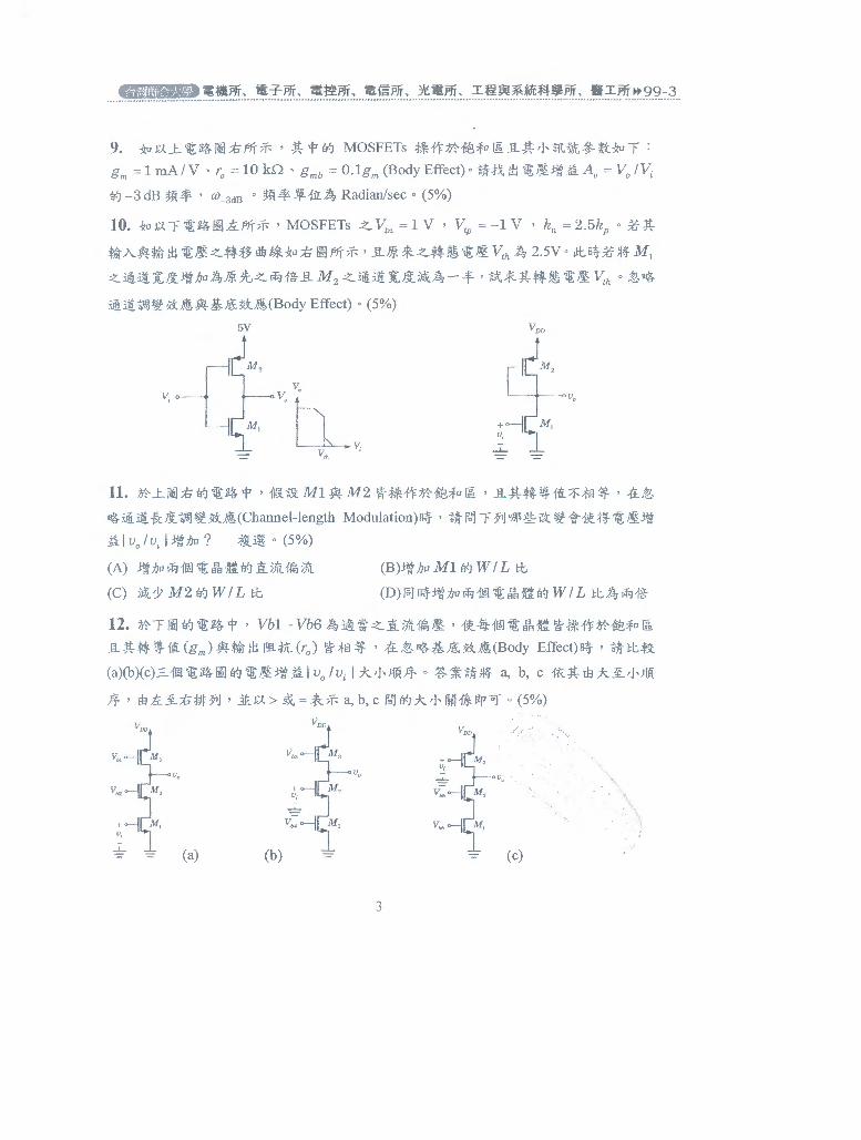
10. -JiuJ..:l.T'it4ml£.P!T~, MOSFETs ~~" =1 V, ~P =-l V, l?.n =2.5 /?.P o %-$.
t,f,]Affi!.t,f,J tl:l 't~~#:f~ aa f#.·lt:a.E m).Pff~ • ll~ *-.~fl.~ i!t;~ Vth ~ 2.5Vo 11:\:.H;lf-_%-~;t lvf1
~ ii! J.! Jt & :li$ /JU 1.9 ~ .7t ~ R91% JL M 2 ~if! J.! Jt & ;~ 1.9 - .f- , 1.>1:. .>f- $,- $H1 't ~ v; h o .~-~
ii!:ilttfol~JitJ.i!f,~£.~3(iJ.i!f, (Body Effect) o (5%)
5V
11. ~ J:. 1@1 .:5 i'f.J i!t4 tf , 1~H9:. Ml ~ M2 i§"~*1"F~~;fu r& , JL.$.--'14 ¥?1a)f:::{El ~ , ~.~.
~ii!J.! -&& 1J!l ~3(ifi.1f,(Channel-length Modulation)B;lf • ~ M T :9 1]·JJ~'l'? ?k ~ -t-1~1-lt- i!tf!1U't ~ I u0 I ui I :1': /Ju? .:ti:il! o (5%)
(A) :l>g /Jo ~ 100 i!t a8a ')Jt i'f.J A iffd~ ;1,t
(C) ;~y M2 i'f.J WI L ~t.
(B):IW /Ja Ml !A WI L ~t.
(D)~ B;lf:l>g /;a ~100 i!t Jla tt !'f.] WI L ~t. ~ ~1%
12. ~TI@lf/.Ji!t~tf' Vbl-Vb6J.93.@'t~Jtiffd~& '1~~100i!t.fla-Jtti§"i*1"f~~;fof& JL$,-#lJ?.-!A(gn,)~t,f,Jtl::~.ll..JJL.(rJ i§";fEJ~ '~.~-~£.M;.3(ifi.1f,(Body Effect)s;lf, 1~~t.~x
(a)(b)(c)~100 i!t4ml !'f.] i!t ~:IW ~I V0 I u; I A+ J11Ji.Jf o ~ ~1~ ~<t a, b, c 1-K.:ft lfJ A.i. +JII~
ff · tb £. .i..E~~ :9'1 , JEJ.:l. > ~ = $z ~ a, b, c M i'f.J A+ ijruf% l'!pOf o (5%)
v.
= (a) (b) = = (c)
3

9 9-4 ~~ GWiUJ.i!!dWtii!!.!ii&f» ...................................... ···············-·-··········-··················-········ ... -- .......... ·-········ ·····- ·······-···· .. ,. ............... -···· .. .. ........................ · -- ~-
13. ~ ;i/f Jt TIE i£ EJiJ it~ · Vb!, Vbz , Vb3 :/;?, 1i ifrt 1~ ~ • -if. it J'a :!It~ .:t#fdt :tiHt!.=fo l& EJiJ
·Mb!L T ' 1H."t~ vo I vi {:(.] :!);~ $- Pf fl.if,:;t_ ~ !Ui 3dB (fH) £-* m M! {:(.] r.,H~Jiit; X ~r ,\f.,l; A±{:(.] ;t~,\f.,l;
(pole);J;-Jt, tifMrJ']"JIII'l!?c.t~i"-1~1-¥-fH.J:',W;I;o? 4~ o (5%)
(A) .l:\W ;/}o !'IT ;1f ift J'a :!It{:(.] A iffd~ iftL (B).J:',W ;l;o M 1 {:(.] [email protected]!Jtlft (W1)
(C) .J:\W;/}o M~ {:([email protected]_Jtlft (W3) (D)t}±it a8a:llt M 4 M~ VDD #-X. M 3 {:(.J)),~i_;t~
uo
+~ u,
14. -1ru.£fJJ4t.k~icu_l:_~;G!'JTif;" o %' MOSFET '/ta8aflt~i;f-11:¥:'-ie;fol& • Jt-~if1~
(gm) ~il; 10 rnA!V • Ji.tR.~i!i!tJ!J~(channel length modulation).&.£~3i.tfi.5(body
effect) o t~.;"j(_ A, = (V01 - V0 z) !(vi! -Viz) :<t.. 113-:!J;~.J:',W ~ o (5%)
15. -1~iU!tJ4t.k~-)(aT~£.!'!Tif;" o ;¥' MOS Jt-~li?W.(g111 ) ~il; l mAN • Ji.~-~i!
i! tJ!J ~ (Channel-Length Modulation) .&. £ ~ 3/.t fl.!!, (Body Effect) o t~ .,"J(_
Au= (V01 -V0 z)l(vi1 -Viz) :<t...-3 dB~$ ' IV_3dB o :!J;~!f-_._1Il.:/;?, Radian/sec o (5%)
',
,· ~
4

16. :{(a J:_ &ij ;6 ?!f:;'G .{£ -100 -¥-:lit 4-.t& 1tr ~(unity-gain buffer) tf • ~A~ A tA fij:j- A.~Jl.:f!L;it
oo • fij:j- t1:: ~llJ!i:.lt 0 o tA:i:R: ft [email protected] it ~J:jW 4- A t1-J :!&. +1H- · 1R.1-lf-1±--{- [email protected] 't4 tf EfJ M
1@4:!:1W 4-llRll'. ~-it (V0 I vi = 1);tl'l.$X:<:.. T"f i'J.:jf +:;¥:- 0.02%Efl* ft.-it o (5%)
17. :!taT &il£.?!f7Gfi.Jl@ft't4 • 1~U~ 't .l'edl!ti-J#-!tlt Vin = 2 V, K, = 0.20 mA/V 2
JL.~-~i!i!m~(Channei-LengthModulation) o ~I:R:ftr\ =v0
IV5
o (5%)
Rs
VDD = lOV
Rd 8kil
r-"'VV\r--+- v.
v.~ --'V\I'v----l f--_._----1
10kil C =co
vo
18. -Jta J:.. &II ;6 PIT-7G o Ql 't .!'a~ g"' = oo o B1 k -11!1&.;fUtA ~ • 't~J:jW 4-lt -1 • f,l:J
A~J!Jit;!t oo • fij:j- tl:: ~J!.:f!L;it 0 o *- 't~J:jW 4_ ~ = V0
I vi o (5%)
19. -JtaT&iJ£.'it4..PIT7G o Q1 gm =oo o B17t.-11!1&.;f!'l~A~ • itl~V1W4-k-1 • f,l:J
A.~Jl.:f!L}t oo • fij:j- tl:: ~J!Jitlt 0 o *- 'tl!Vw 4-~ = V0 I vi tl-] -3 dB -Jj;Ji. Jt • UJ0
(rad/sec) o (5%)
v.
v:
v, =
4 (Transfer Function) o $,. 'f a(s) = ---
1 +sf p 1
p 2 = lx106 rad/sec • fJ = 0.5 o .;JUtt111p1 .3UOJ"11Bi- • Jl:!:.~M,:jf 45° tl-] Phase Margin o
tij-Jfi Bode Plot ti-J:liii:-o"RJW. o (5%)
5