ekv3.0 mos transistor model for advanced analog … users’ meeting/workshop, epfl, november 4-5,...
TRANSCRIPT

EKV Users’ Meeting/Workshop, EPFL, November 4-5, 2004
EKV3.0 MOS Transistor Modelfor Advanced Analog IC Design
Matthias Bucher, TUCFrançois Krummenacher, EPFL
Antonios Bazigos, NTUA
[email protected] & Computer Engineering Department
Technical University of Crete (TUC)GR-73100 Chania, Crete, Greece

M. Bucher TUC 2004 2EKV3.0 Workshop, EPFL, Nov. 4-5, 2004
EKV team & contributors to EKV3.0
Team of universities contributing to EKV model R&D: EPFL, TUC/NTUA, U. Strasbourg
François Krummenacher, Christian Enz, Eric VittozJean-Michel Sallese, Wladek Grabinski, Ananda RoyMatthias Bucher, Antonios BazigosAlain-Serge PorretChristophe Lallement, Fabien Pregaldiny
Code development: TUC/NTUACoordination with EPFL

M. Bucher TUC 2004 3EKV3.0 Workshop, EPFL, Nov. 4-5, 2004
The EKV2.6 model
Developed at EPFL, 1997 [PhD M. Bucher]Same physical basis as EKV3.0-- first widely used “charge linearization” model< 20 parameters, many “analog” featuresAvailable in many circuit simulators
ADS, AMI-Spice, Antrim-A/MS, APLAC, ELDO, IntuSoft, HSIM, LTspice/SwitcherCAD, Star-Hspice, MacSpice, Micro-CapV, MINIMOS-NT, MI-SUGAR, NanoSpice, Nexxim, NG-Spice, PSpice, SABER, SANCAD, SIMetrix, SmartSpice, SMASH, Spectre, SpectreRF, SPICE3, Spice-Opus, Synopsys, TopSPICE, TRANZ-TRAN, T-Spice, WinSpice …
http://legwww.epfl.ch/ekv/model.html#availabilityMainly used by analog IC design teams
Fabless companiesNokia, Xemics, Tektronix, Microen, CSEM, Advanced Silicon, …
Foundries/vertically integratedToshiba, Atmel, Microchip, Microelectronic Marin, NEC, …
Many universities & research institutesEPFL, ETHZ, UNCC, CERN, LETI …

M. Bucher TUC 2004 4EKV3.0 Workshop, EPFL, Nov. 4-5, 2004
EKV3.0 outline – basis & motivation
Motivation: Efficient, truly compact model including for sub-100nm CMOSPhysical basis, predictivity & dependable behaviourLow number of parameters, scalable, non-binnedAddressing design needs in advanced analog IC designCo-development of design methodologies and characterization methods
EKV3.0 MOST model for next generation CMOS Evolution from EKV2.6, address known shortcomings High level of code standardizationNext generation model standard evaluation (CMC procedure)

M. Bucher TUC 2004 5EKV3.0 Workshop, EPFL, Nov. 4-5, 2004
Outline
EKV3.0 model structureCharge model basicsLocal/integral charge modelPolydepletion & quantum effects [François Krummenacher]
Short-channel capacitance modelCharge-based mobility modelShort-channel effectsBenchmarking
Level-of inversion-centered view of the MOSTSummary
M. Bucher TUC 2004 6EKV3.0 Workshop, EPFL, Nov. 4-5, 2004
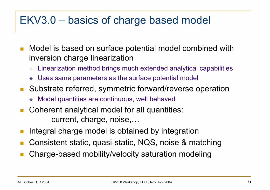
EKV3.0 – basics of charge based model
Model is based on surface potential model combined with inversion charge linearization
Linearization method brings much extended analytical capabilitiesUses same parameters as the surface potential model
Substrate referred, symmetric forward/reverse operationModel quantities are continuous, well behaved
Coherent analytical model for all quantities:current, charge, noise,…
Integral charge model is obtained by integrationConsistent static, quasi-static, NQS, noise & matchingCharge-based mobility/velocity saturation modeling

M. Bucher TUC 2004 7EKV3.0 Workshop, EPFL, Nov. 4-5, 2004
Surface potential in MOS structure
60
40
20
0
ΨS /
UT
[-]
200150100500-50-100
(VG- VFB) / UT [-]
n-channel2*ΦF = 0.9 V
γ = 0.5 V1/2
2*ΦF / UT
ΦF / UT
Acc
umul
atio
n
Dep
letio
n
Wea
k
Mod
erat
e
S
tron
g In
vers
ion
Vch / UT = 0
Charge & voltage balance:
ox
ibSFBG C
QQVV′+′
−Ψ=−
100
50
0
-50
-100
Tota
l Cha
rges
Q /
(UTC
oxW
L)
3.02.52.01.51.00.50.0-0.5-1.0-1.5
VG [V]
VD=VS=0V
VTO=0.5V γ=0.6V1/2
Ψ0=1V
QS=QD
QG
QB
QI

M. Bucher TUC 2004 8EKV3.0 Workshop, EPFL, Nov. 4-5, 2004
Inversion charge linearization (I)
Inversion charge vs. surface potential (fixed VG) is essentially linearExplicit use of linearization defines charge linearization factor nq
Intersection with x-axis defines pinch-off surface potential ΨΨΨΨp
Related concepts of pinch-off voltage Vp = ΨΨΨΨp – ΨΨΨΨ0 and slope factor nvUse the same parameters (TOX, NSUB, VFB) as surface potential model
ox
subsisFBG
sssFBGP C
NqwhereVVVV
′=
−+−⋅+−=Ψ
εγγγγ
2)
2(
22
PΨ
M. Bucher TUC 2004 9EKV3.0 Workshop, EPFL, Nov. 4-5, 2004
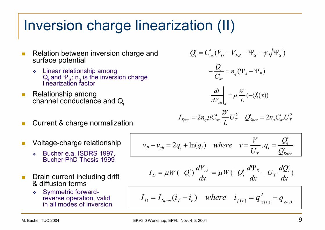
Inversion charge linearization (II)
Relation between inversion charge and surface potential
Linear relationship amongQi and ΨS: nq is the inversion charge linearization factor
Relationship amongchannel conductance and Qi
Current & charge normalization
Voltage-charge relationshipBucher e.a. ISDRS 1997,Bucher PhD Thesis 1999
Drain current including drift& diffusion terms
Symmetric forward-reverse operation, validin all modes of inversion
)( SSFBGoxi VVCQ Ψ−Ψ−−′=′ γ
)( PSqox
i nCQ
Ψ−Ψ=′′
−
)()(dxQdU
dxdQW
dxdVQWI i
TS
ich
iD′
+Ψ′−=′−= µµ
22 22 ToxqSpecToxqSpec UCnQULWCnI ′=′′= µ
)()(
2)()(
DiSDiSqqiwhereiiII rfrfSpecD +=−=
))(( xQLW
dVdI
ixch
′−= µ
Spec
ii
TiichP Q
QqUVvwhereqqvv
′′
==+=− ,)ln(2

M. Bucher TUC 2004 10EKV3.0 Workshop, EPFL, Nov. 4-5, 2004
EKV3.0 outline – higher-order effects
Non-uniform doping effects: Vertical/lateral non-uniform doping effectsRSCE, pocket/halo doping related effects
High-field effects, advanced technology:Polydepletion & quantum effectsGate tunnelling current, GISDL, substrate current
Charge-based mobility modelling:Vertical field mobility based on effective fieldVelocity saturation/channel length modulation
Short-channel effects:DIBL, charge-sharingINWE, combined short&narrow-channel effects
Bias-dependent parasitics modelling:Overlap charge/capacitance modelBias-dependent series resistance model
Temperature effects

M. Bucher TUC 2004 11EKV3.0 Workshop, EPFL, Nov. 4-5, 2004
EKV3.0 outline – additional features
2nd-order scaling of parameters:Includes length-dependence of mobilitySTI-stress related effects
Non-quasistatic AC modelCompanion model for transient under development
Noise:1/f noiseShort-channel thermal noiseInduced noise in gate and substrate
More analog-design oriented features:Local mismatch models built-inFeedback to designer w.r.t. level-of-inversion, tef, GBW, ....
Choice of use: physical OR electrical parameters

M. Bucher TUC 2004 12EKV3.0 Workshop, EPFL, Nov. 4-5, 2004
EKV3.0 charge model – higher-order effects
Polydepletion & quantum effects (PDE & QME)Modeling of short-channel effects in charge/capacitances
Basic channel/gate doping (RSCE), ….…. & 2D effects (DIBL, CS) propagate into the charges modelEffective channel length for charges/capacitances:
LeffC = L + XL + DL + DLCAccounting for CLM & VSAT also in transcapacitances
Bias-dependent overlap charge modelInner fringing charge/capacitance

M. Bucher TUC 2004 13EKV3.0 Workshop, EPFL, Nov. 4-5, 2004
MOS capacitor/varactor modeling
0.0E+00
5.0E-11
1.0E-10
1.5E-10
2.0E-10
-5 -4 -3 -2 -1 0 1 2 3 4 5
VG
CG
Model can be used to model MOS varactorsPDE may occur in accumulation for opposite type of gate
Choice of the type of gate with a model parameter TGOnly change is for NGATE, VFB
P-WELL
N-GATEP-GATE

M. Bucher TUC 2004 14EKV3.0 Workshop, EPFL, Nov. 4-5, 2004
Long-channel CV – 0.12um CMOS
C11n NM OS L ong-W ide
0,0E+00
5,0E-11
1,0E-10
1,5E-10
2,0E-10
2,5E-10
3,0E-10
3,5E-10
-1,5 -1 -0,5 0 0,5 1 1,5VG [V]
C [F
]
CGGEKV3.0CGCEKV3.0CGBEKV3.0
L = 10um
= 7 V-1/2+GAMMAG= 200m V-1/2+GAMMA= 250m V+VTO= 12m F/m2+COX= 400m V+PHIF

M. Bucher TUC 2004 15EKV3.0 Workshop, EPFL, Nov. 4-5, 2004
Overlap charge/capacitance
Model of (direct) Gate-to-S/D overlapLocal charge model w. depletion/accumulationSimilar as for varactor modelingHigher-order effects: QME, PDEOverlap parameters:
VFBOV – Flat-band voltage of Gate-S/D overlap NOV [GAMMAOV] – Overlap region doping conc.LOV – Gate-S/D overlap region length

M. Bucher TUC 2004 16EKV3.0 Workshop, EPFL, Nov. 4-5, 2004
Short-channel CV – 0.12um CMOS
C11n PMOS Short-Wide
0,0E+00
5,0E-12
1,0E-11
1,5E-11
2,0E-11
2,5E-11
3,0E-11
3,5E-11
-1,5 -1 -0,5 0 0,5 1 1,5-VG [V]
C [F
] CGGEKV3.0CGCEKV3.0CGBEKV3.0
Short-channel CV (L=0.12um) with example parametersNeed to add inner fringing term
L = 0.12um= 2.5 V-1/2+GAMMAOV= 20n m+LOV= 0 V+VFBOV

M. Bucher TUC 2004 17EKV3.0 Workshop, EPFL, Nov. 4-5, 2004
Inner fringing capacitance
Charge-based model, empirically based but essentially related to surface potential at source/drain
G. Gildenblat e.a., IEDM Tech. Digest 2003
2 empirical fitting parameters, AIF, BIF
( )
DIFSIFG
SXXbiXIFIFXIF
QQQDSXwhere
VVVBAQ
,,
,
,1
∆−∆−=∆=
Ψ−+⋅+⋅=∆

M. Bucher TUC 2004 18EKV3.0 Workshop, EPFL, Nov. 4-5, 2004
Capacitance benchmarks (I)
Smooth, well-behaved CV modelFrom accumulation to depletion and inversionFrom linear to saturation

M. Bucher TUC 2004 19EKV3.0 Workshop, EPFL, Nov. 4-5, 2004
Capacitance benchmarks (II)
0.0E+00
2.0E-10
4.0E-10
6.0E-10
8.0E-10
1.0E-09
1.2E-09
-1.5 -1 -0.5 0 0.5 1 1.5
VGB [V]
CG
G [F
]
-2.0E-09
-1.0E-09
0.0E+00
1.0E-09
2.0E-09
3.0E-09
4.0E-09
-1.5 -1 -0.5 0 0.5 1 1.5
VGB (V)
dCG
G/d
VGB
(F/V
)

M. Bucher TUC 2004 20EKV3.0 Workshop, EPFL, Nov. 4-5, 2004
EKV3.0 mobility modeling (I)
Mobility versus VG, VD – EKV3.0 simulationCoulomb scattering (low Eeff), surface roughness scattering (high Eeff)Saturation behaviour is included naturally

M. Bucher TUC 2004 21EKV3.0 Workshop, EPFL, Nov. 4-5, 2004
EKV3.0 mobility modeling (II)Effective-field based mobility modeling
Surface-roughness scattering (high vertical field)
Phonon-scattering intermediate field strengths
Coulomb scattering effects(low vertical field; particularly at very high Nsub, low T)
Local mobility is integrated along the channel
5 parameters in all:E0, E1, ETA, THC, ZC
ibeff QQE ⋅+∝ η

M. Bucher TUC 2004 22EKV3.0 Workshop, EPFL, Nov. 4-5, 2004
Velocity saturation modelingConsider a variable-order (1st-2nd) velocity-field relationship
Requires 2 parameters:
UCRIT, DELTA [1..2]
New charge-based channel length modulation (CLM) model.
Continuous at VD=VS
LAMBDA

M. Bucher TUC 2004 23EKV3.0 Workshop, EPFL, Nov. 4-5, 2004
Gummel symmetry test
EKV3.0 fulfills Gummel symmetry testAll model aspects (mobility, velocity saturation, CLM, DIBL, CS,…) are formulated symmetrically
-0.2 -0.1 0 0.1 0.2VDS (V)
dID
/dVD
S (A
/V)
-0.2 -0.1 0 0.1 0.2VDS [V]
ID (l
og. a
xis)
M. Bucher TUC 2004 24EKV3.0 Workshop, EPFL, Nov. 4-5, 2004
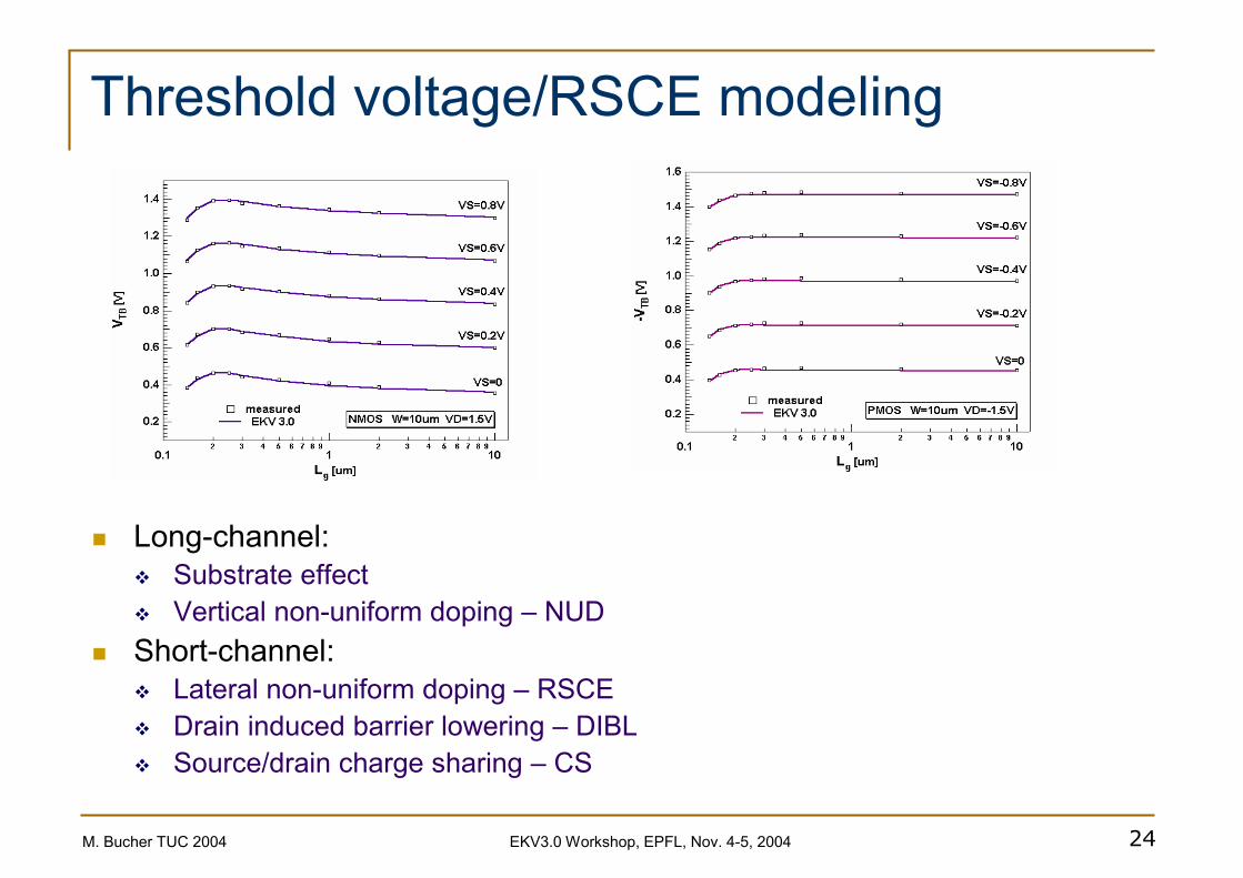
Threshold voltage/RSCE modeling
Long-channel: Substrate effectVertical non-uniform doping – NUD
Short-channel: Lateral non-uniform doping – RSCEDrain induced barrier lowering – DIBLSource/drain charge sharing – CS

M. Bucher TUC 2004 25EKV3.0 Workshop, EPFL, Nov. 4-5, 2004
Drain induced barrier lowering
Drain Induced Barrier Lowering
0
10
20
30
40
50
60
70
80
90
100
0 0.1 0.2 0.3 0.4 0.5 0.6 0.7 0.8 0.9 1
Channel Coordinate x/L [-]
Surf
ace
Pote
ntia
l V/U
T [-]
L=90nm APPROX.L=90nm EXACTL=10um
Quasi-2D solution for Surface potential, Liu e.a. IEEE TED’93Symmetric wrt. VD, VSApproximation uses one single exponential -- no bias dependence in exponential
DIBL model scales with Tox, Nsub, T!2 Parameters ETAD
00 Ψ∝sub
siqNL γε

M. Bucher TUC 2004 26EKV3.0 Workshop, EPFL, Nov. 4-5, 2004
EKV3.0 – short-channel characteristics
Correct weak & moderate inversion behaviorSmoothness and correct asymptotic behaviorCorrect weak inversion slope and DIBL modeling
Transconductance-to-current ratio vs. drain current (log. axis)
L=70nm VD=1.5V
0.0E+00
1.0E-01
2.0E-01
3.0E-01
4.0E-01
5.0E-01
6.0E-01
7.0E-01
8.0E-01
1.00E-08 1.00E-07 1.00E-06 1.00E-05 1.00E-04 1.00E-03 1.00E-02
ID [A]
GM
*UT/
ID [-
]
measuredEKV3.0
L=70nm VD=1.5V
1.0E-10
1.0E-09
1.0E-08
1.0E-07
1.0E-06
1.0E-05
1.0E-04
1.0E-03
1.0E-02
0 0.2 0.4 0.6 0.8 1 1.2 1.4 1.6 1.8
VG [V]
ID [A
]
measuredEKV3.0
L = 70nm

M. Bucher TUC 2004 27EKV3.0 Workshop, EPFL, Nov. 4-5, 2004
EKV3.0 output characteristics modeling
L=70nm VB=0V
0.0E+00
1.0E-03
2.0E-03
3.0E-03
4.0E-03
5.0E-03
6.0E-03
7.0E-03
8.0E-03
9.0E-03
0 0.2 0.4 0.6 0.8 1 1.2 1.4 1.6 1.8
VD [V]
ID [A
]
measuredEKV3.0
L=70nm VB=-1V
0.0E+00
1.0E-03
2.0E-03
3.0E-03
4.0E-03
5.0E-03
6.0E-03
7.0E-03
8.0E-03
0 0.2 0.4 0.6 0.8 1 1.2 1.4 1.6 1.8
VD [V]
ID [A
]
measuredEKV3.0
L=70nm VB=0V
1.0E-04
1.0E-03
1.0E-02
1.0E-01
0 0.2 0.4 0.6 0.8 1 1.2 1.4 1.6 1.8
VD [V]
gds
[A/V
]
measuredEKV3.0
L=70nm VB=-1V
1.0E-05
1.0E-04
1.0E-03
1.0E-02
1.0E-01
0 0.2 0.4 0.6 0.8 1 1.2 1.4 1.6 1.8
VD [V]
gds
[A/V
]
measuredEKV3.0
L = 70nm

M. Bucher TUC 2004 28EKV3.0 Workshop, EPFL, Nov. 4-5, 2004
Ongoing R&D for EKV
Noise modeling:Short-channel thermal noise modelingNQS noise modeling: induced noise in gate and substrate
NQS effects in transient analysisModeling of generation/recombination effects in PD SOIDouble-gate MOSFETDegradation of output conductance in long-channel MOSFETs due to pocket implant

M. Bucher TUC 2004 29EKV3.0 Workshop, EPFL, Nov. 4-5, 2004
Inversion-level centered design method
Transconductance to current ratio is a central design variableDedicated measurement method has been developed to measure all transconductances vs. normalized drain currentMethod is useful for:
Understanding of CMOS process complexityDirect input to designDevelopment of hand-calculation modelParameter extractionVerification of circuit simulation model
Method to be complemented with HF gain, linearity, matching, noise,….

M. Bucher TUC 2004 30EKV3.0 Workshop, EPFL, Nov. 4-5, 2004
EKV3.0 -- normalized transconductances in 0.25um CMOS
0
0.1
0.2
0.3
0.4
0.5
0.6
0.7
0.8
1E-06 0.00001 0.0001 0.001 0.01 0.1 1 10 100 1000
IC
gmg
* UT
/ ID
L=5umL=0.28um
IC – Inversion Coefficient (in saturation)Source-, gate, substrate transconductance vs. IC
G(IC) function and slope factor n allow to easily express normalized transconductance vs. Level of inversion
Exception in strong inversion/short channel (due to vel. Sat.)
0
0.1
0.2
0.3
0.4
0.5
0.6
0.7
0.8
0.9
1
1E-06 0.00001 0.0001 0.001 0.01 0.1 1 10 100 1000
IC
gms
* U
T / I
D
L=5umL=0.28um
0
0.1
0.2
0.3
0.4
1E-06 0.00001 0.0001 0.001 0.01 0.1 1 10 100 1000
IC
gmb
* UT
/ ID
L=5umL=0.28um
ICICG
++=
41
21
1)(nICG
IUg
D
Tm )(= )(1 ICG
nn
IUg
D
Tmb −=)(ICG
IUg
D
Tms =

M. Bucher TUC 2004 31EKV3.0 Workshop, EPFL, Nov. 4-5, 2004
EKV3.0 -- output conductance & self-gain in 0.25um CMOS
10
100
1000
10000
1E-06 1E-05 0.0001 0.001 0.01 0.1 1 10 100 1000
IC
gmg
/ gm
d
0.00001
0.0001
0.001
0.01
0.1
1E-06 1E-05 1E-04 0.001 0.01 0.1 1 10 100 1000IC
gmd
* UT
/ ID
EKV3.0 shows excellent gmd*UT/ID modelling with IC, L
L ranges from 0.28um to 5um
DC self-gain is maximum in weak inversion, long-channel!
D
T
D
P
D
Tds
Vn
nU
VVICG
IUg
∂∂
+∂∂
≅ )(
M. Bucher TUC 2004 32EKV3.0 Workshop, EPFL, Nov. 4-5, 2004
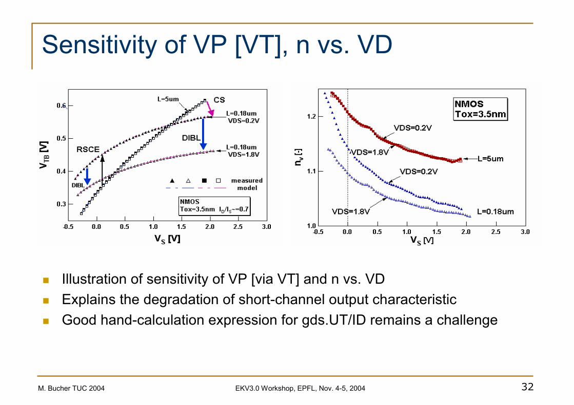
Sensitivity of VP [VT], n vs. VD
Illustration of sensitivity of VP [via VT] and n vs. VDExplains the degradation of short-channel output characteristicGood hand-calculation expression for gds.UT/ID remains a challenge

M. Bucher TUC 2004 33EKV3.0 Workshop, EPFL, Nov. 4-5, 2004
EKV3.0 – normalized transconductance 0.13um CMOS

M. Bucher TUC 2004 34EKV3.0 Workshop, EPFL, Nov. 4-5, 2004
Shallow-trench isoloation (STI) effect
Narrow devices are affected by stress due to vicinity of ST IsolationDegrades G(IC) function in moderate inversionSTI stress is an important effect in CMOS <0.18um generations

M. Bucher TUC 2004 35EKV3.0 Workshop, EPFL, Nov. 4-5, 2004
Halo/pocket implant effect on norm. gds, 0.13um CMOS
Anomalous scaling of output conductance [gds*UT/ID] at fixed level of inversion vs. channel length (meas. only)
A dedicated characterization technique has been developed Scaling: L-3 (short-channel, weak inversion), L-0.6 (long-channel)Pocket/halo implants degrade medium-long channel gds scaling-- severe issue for analog. New model under development.
Weak inversion: IC<0.1Moderate inversion: 0.1< IC<10
Strong inversion: IC>10
M. Bucher, D. Kazazis, F. Krummenacher,WCM-NANOTECH, Boston, March 2004

M. Bucher TUC 2004 36EKV3.0 Workshop, EPFL, Nov. 4-5, 2004
EKV3.0 summary (I)
EKV3.0, a physics-based, design-oriented compact modelCharge linearization principleCoherent framework for static-dynamic model, NQS, noise, matchingContinuous, symmetric forward-reverse operationSupports advanced analog IC design practice
EKV3.0 validated for 0.11um CMOSIncludes all major physical effects for present CMOS technologiesFavorable efficiency/complexity trade-offNumber of parameters: ~ 50 (basic intrinsic) + 20 (2nd order scaling)90nm CMOS validation underway

M. Bucher TUC 2004 37EKV3.0 Workshop, EPFL, Nov. 4-5, 2004
EKV3.0 summary (II)
EKV3.0 for next generation CMOSExtension of EKV formalism to SOI, double gate, FinFETs, ballistic MOSFET under developmentHVMOS MOSFET model under investigation
EKV3.0 for public-domainCode standardization using Verilog-AMSImplementations being tested in several simulatorsEKV3.0 model release: “Light Edition” (2004)
ELDO beta release Jan. 2005
M. Bucher TUC 2004 38EKV3.0 Workshop, EPFL, Nov. 4-5, 2004
Acknowledgments
Infineon, Toshiba, Mentor Graphics
All EKV team
Isabelle Buzzi

M. Bucher TUC 2004 39EKV3.0 Workshop, EPFL, Nov. 4-5, 2004
Selected references on EKV3.0 (I)
Online References [admin. W. Grabinski]: http://legwww.epfl.ch/ekv
J.-M. Sallese, F. Krummenacher, P. Fazan, “Derivation of Shockley-Read-Hall Recombination Rates in Bulk and PD SOI MOSFET’s Channels Valid in All Modes of Operation, Solid State Electronics, Vol. 48, (in press) 2004.A. Bazigos, M. Bucher, S. Yoshitomi, “Benchmarking the EKV3.0 MOSFET Model in Verilog-A with 0.14µm CMOS, 11th Int. Conf. on Mixed Design (MIXDES 2004), pp. 104-109, Scezcin, Poland, June 24-26, 2004.A. S. Roy, C. Enz, “Compact Modeling of Thermal Noise in the MOS Transistor”, 11th Int. Conf. on Mixed Design (MIXDES 2004), pp. 71-78, Scezcin, Poland, June 24-26, 2004.P. Martin, M. Bucher, “Comparison of 0.35 and 0.21 µm CMOS Technologies for Low Temperature Operation (77 K-200 K) and Analog Circuit Design”, Workshop on Low-Temperature Electronics (WOLTE 6), ESA/ESTEC, Noordwijk, The Netherlands, June 2004.C. Enz, A. S. Roy, “A Comprehensive Study of Thermal Noise in the MOS Transistor”, SPIE Symp. on Fluctuation & Noise, Maspalomas, Spain, May 2004.A.-S. Porret, C. C. Enz, “Non-Quasi-Static (NQS) Thermal Noise Modeling of the MOS Transistor”, IEE Proc. Circuits, Devices and Syst., 2004.______, SPIE Int. Symp. on Fluctuation and Noise, Santa Fe, USA, June 2003.M. Bucher, D. Kazazis, F. Krummenacher, “Geometry- and Bias-Dependence of Normalized Transconductances in Deep Submicron CMOS”, Workshop on Compact Models, NANOTECH 2004, Boston, March 2004. [Available Online: http://www.ntu.edu.sg/home/exzhou/WCM/WCM2004/wcm04.htm#Slides]C. Lallement, J.-M. Sallese, M. Bucher, W. Grabinski, P. Fazan, "Accounting for Quantum Effects and Polysilicon Depletion from Weak to Strong Inversion in a Charge-Based Design-Oriented MOSFET Model", IEEE Trans. Electron Devices , Vol. 50, N° 2, pp. 406-417, February 2003.

M. Bucher TUC 2004 40EKV3.0 Workshop, EPFL, Nov. 4-5, 2004
Selected references on EKV3.0 (II)
J.-M. Sallese, M. Bucher, F. Krummenacher, P. Fazan, "Inversion Charge Linearization in MOSFET Modeling and Rigorous Derivation of the EKV Compact Model", Solid-State Electronics, Vol. 47, pp. 677-683, 2003.M. Bucher, D. Kazazis, F. Krummenacher, D. Binkley, D. Foty, Y. Papananos, “Analysis of Transconductances at All Levels of Inversion in Deep Submicron CMOS”, 9th IEEE Conf. on Electronics, Circuits and Systems (ICECS 2002), pp. 1183-1186, Dubrovnik, Croatia, September 2002.M. Bucher, J.-M. Sallese, F. Krummenacher, D. Kazazis, C. Lallement, W. Grabinski, C. Enz, “EKV3.0: An Analog Design-Oriented MOS Transistor Model” 9th Int. Conf. on Mixed Design (MIXDES 2002), Wroclaw, Poland, June 2002.P. Martin, M. Bucher, C. Enz, “MOSFET Modeling and Parameter Extraction for Low Temperature AnalogCircuit Design”, Journal de Physique IV, N° 12, 2002, Pr. 3, pp. 51-56, Les Editions de Physique, Les Ulis, France.M. Bucher, C. Enz, F. Krummenacher, J.-M. Sallese, C. Lallement, A.-S. Porret, “The EKV3.0 Compact MOS Transistor Model: Accounting for Deep Submicron Aspects”, Workshop on Compact Models-MSM 2002, pp. 670-673, Puerto Rico, April 2002.C. Enz, M. Bucher, A.-S. Porret, J.-M. Sallese, F. Krummenacher, “The Foundations of the EKV MOS Transistor Charge Based Model”, Workshop on Compact Models-MSM 2002, pp. 666-669, Puerto Rico, April 2002.C. Enz, “An MOS Transistor Model for RF IC Design Valid in All Regions of Operation”, IEEE Trans. Microwave Theory and Tech., Vol. 50, N° 1, pp. 342-359, January 2002.M. Bucher, J.-M. Sallese, C. Lallement, “Accounting for Quantum Effects and Polydepletion in an Analytical Design-Oriented MOSFET Model”, Simulation of Semiconductor Processes and Devices (SISPAD 2001),pp. 296-299, Ed. D. Tsoukalas, C. Tsamis, Springer, ISBN 3-211-83708-6, 2001.A.-S. Porret, J.-M. Sallese, C. Enz, “A Compact Non Quasi-Static Extension of a Charge-Based MOS Model”, IEEE Trans. Electron Devices, Vol. 48, N° 8, pp. 1647-1654, August 2001.

M. Bucher TUC 2004 41EKV3.0 Workshop, EPFL, Nov. 4-5, 2004
Selected references on EKV3.0 (III)
J.-M. Sallese, M. Bucher, C. Lallement, “Improved Analytical Modeling of Polysilicon Depletion in MOSFETs for Circuit Simulation”, Solid-State Electronics, Vol. 44, N° 6, pp. 905-912, June 2000.J.-M. Sallese, A.-S. Porret, “A Novel Approach to Non-Quasi-Static Model of the MOS Transistor Valid in All Modes of Operation”, Solid-State Electronics, Vol. 44, N° 6, pp. 887-894, June 2000.C. Enz, Y. Cheng, “MOS Transistor Modeling for RF IC Design”, IEEE Trans. Solid-State Circuits, Vol. 35, N° 2, pp 186-201, February 2000.M. Bucher, "Analytical MOS Transistor Modelling for Analog Circuit Simulation", Ph. D. Thesis N° 2114,Swiss Federal Institute of Technology (EPFL), Lausanne, Switzerland, 1999.M. Bucher, C. Enz, C. Lallement, F. Theodoloz, F. Krummenacher, “Scalable GM/I Based MOSFET Model”, Int. Semicond. Dev. Res. Symp. (ISDRS’97), pp. 615-618, Charlottesville, Virginia, December 1997.M. Bucher, C. Lallement, C. Enz, “An Efficient Parameter Extraction Methodology for the EKV MOST Model”, Proc. IEEE ICMTS, Vol. 9, pp. 145-150, March 1996.C. C. Enz, F. Krummenacher, E. A. Vittoz, “An analytical MOS Transistor Model Valid in All Regions of Operation and Dedicated to Low-Voltage and Low-Current Applications”, J. AICSP, Vol. 8, pp. 83-114, 1995.

M. Bucher TUC 2004 42EKV3.0 Workshop, EPFL, Nov. 4-5, 2004
Contact
Matthias BucherAssistant Professor
Technical University of CreteDept. of Electronics & Comp. Eng.73100 Chania, Crete, Greece
phone: +30 28210 37210fax: +30 28210 [email protected]