efficient partitioning for the batch-fabricated fourth ... · efficient partitioning for the...
TRANSCRIPT
Efficient partitioning for the batch-fabricated fourth generation computer
by N. CSERHALMI, O. LOWENSCHUSS and B. SCHEFF
Raytheon Company Bedford, Massachusetts
INTRODUCTION
The computer industry is on the verge of an upheaval, due to drastically new hardware and modern computational concepts. Read-only memories which operate near 0.1 microseconds are available, while large-scale integration (LSI) offers the promise of inexpensive, batch fabricated processing of logic and storage elements. The problem which confronts the computer designer is how to use these elements in an efficient manner to take full advantage of their speed and flexibility. Many approaches have been proposed, but none have shown a clear solution to the problem. The concept presented in this paper is the result 'Of extensive development activities.
The partitioning problem
A study of both general and special purpose digital hardware indicates that certain basic arithmetic and Boolean functions are repeated in various combinations throughout a given computer system. Presently available c'Omplex logic arrays such as adders, shift registers, and counters perform many of these tasks, and reduce logic cost, compared to the use of simple gates. At the same time they create a serious logistics problem to the hardware product engineer, because stock and maintenance parts increase. In a rapidly growing technology, where labor is so costly, the design, procurement, fabrication, and test cycles are all lengthened by the needs for many different types of parts. By. combining several related operations into a single array, significant improvements in logistics, interconnect ratios, powerspeed merit figures, and component l'Ogic efficiency are realized.
An array can be fabricated with dIscretionary wiring methods (slice technology) or with the hcell approach" (chip technology), or with hybrid technology. From the component point of view, bipolar or MOS devices may be used.
The size and the complexity of the array is determined by the logic partitioning. The proper selection of the components 'and interconnection method is dictated by packaging, power consumption, performance, and economic considerations.
How can one tell whether the partitioning is right? Two numeric criteria provide a measure for any given partitioning design;
857
a) Maximum Gate/Pin Ratio-This ratio is generally between 0.1 to 0.6 in present integrated circuit (IC) systems. A ratio near 1 is considered outstanding. With the LSI building blocks described below, a ratio of 3 to 10 can be achieved. The requirement for increased gate/pin ratio is a basic reason for the existence of LSI arrays, because interconnections on the microelectronics level are less expensive and more reliable than at the package level.
b) Minimum Number 0/ Array Types (Partnumbers ) -This is the best criterion of the logic partitioning, and demonstrates the level of coordination between semicond.uctor, logic and, system designers. Most IC systems employ from 50 to 100 types of printed-circuit modules. Minimum "part-numbers" is one of the primary requirements in all military systems, and is an economics requirement for commercial and low-volume production sys-
From the collection of the Computer History Museum (www.computerhistory.org)
858 Fall Joint Computer Conference, 1968
tems. Several digital IC systems (including general purpose computers) have been built that contain 3 to 15 types of printedcircuit plug-in boards at 40 or more gates per board.
The penalty paid for maximum gate-pin ratio and minimum part numbers is an inefficiency in the use of silicon (gates) and hence of power. Thus, in "tight" applications such as space vehicles, the designer might prefer to forego the economic advantages of this type of partitioning in favor of minimum power.
Directions in LSI computer architecture
Current developments
With LSI technology progressing toward maturity, more useful documents are being published in the field of LSI system architecture. Most assume the unlimited success of the semiconductor process, but only a few cite documented hardware development. LSI development projects, either completed or near completion, differ in their partitioning concepts; all are designed to replace third generation computers in whole or in part. Some of these development projects are briefly described to supply a background to this paper.
1) The sole producer of discretionary wiring (or slice technology), Texas Instruments, has designed and built an LSI airborne computer, the Model 2502. This generalpurpose 16-bit word computer consists of a Central Processing Unit (CPU) and a 3-channel Input/Output Unit. The single address CPU is controlled by a 2 MHz clock, and the 36-instruction set is executed through four general purpose registers. (Reference 1)
From the partitioning point of view, the most significant feature is that the CPU is implemented with 16 identical arrays, which include all arithmetic and register functions except for the control logic. The elimination of "special-purpose" registers (index, accumulator, etc.) must also be emphasized. While the GPU is partitioned on a bit basis, the three I/O channels are implemented by six arrays of another type, partitioned on a functional basis. A gate-to-pin ratio of two was achieved on both arrays.
Although automated design was used to assist in the implementation of the control logic, the use of ten different arrays with low gate-to-pin ratios was required. Another disadvantage is that the industrywide claims of LSI speed improvements do not appear; the computer is three to five times slower than is attainable using currently mass-produced TTL circuits.
2) A larger and more powerful general.,.purpose aerospace computer has been designed (hardware near completion) at Raytheon Company. This parallel 32-bit word computer offers 94 instructions, in-
. definite chaining of Index and Indirect Addressing, and Multiprocessor capability. The seven full-length registers of the CPU are partitioned into eight identical arrays. Each array contains four stages of all seven registers, including the transfer gate structure. These eight LSI Arrays of one type contain 56 percent of the entire CPU logic.
The control logic is temporarily implemented with 14-lead TTL circuits. Some further work is being done to replace the majority of control with a Read-Only Memory (ROM), leaving only less than five percent non-LSI hardware.
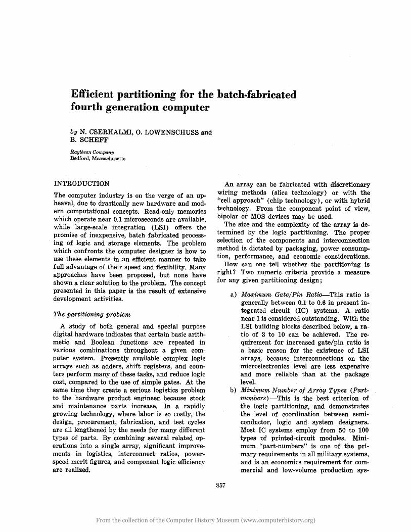
3) In another Raytheon development program, a CPU is under construction which utilizes 25 "Raytheon AS-80" arrays. This multi-purpose 4-bit Counter/Register is used as a building block to form the eleven working registers which are 4, 8, or 16 bits long. The block diagram of this ar-
3-BIT FUNCTION CODE
SERIAL DATA INPUT (SHIFT RIGHT)
COUNT IN
CARRY OUT
CLOCK ENABLE MASTER RESET
PARALLEL DATA INPUTS
X Y L
COUNTER/REGISTER CONTENTS
SERIAL DATA INPUT
(SHIFT LEFT)
FIGURE l-Multi-purpose counter/register
From the collection of the Computer History Museum (www.computerhistory.org)
Efficient Partiti'Oning f'Or· Batch-Fabricated C'Omputer 859
ray is sh'Own in Figure 1; it will be described in detail in a later part 'Of this paper.
The pr'Ocess'Or is a 16-bit, parallel, singleaddress, high-speed unit. Operating with a· s'Olid-state, read/write mem'Ory, it can execute an add instructi'On in less than 1f2 ~sec, and a 16-bit multiply in less than 2 fJsec average.
Fr'Om a partiti'Oning P'Oint 'Of view, the CPU is 'Organized as f'Oll'OWS :~O percent 'Of the I'Ogic is implemented by tW'O types 'Of arrays (Raythe'On AS-80 and Signetics 8260) and the remaining 20 percent is implemented by high-speed TTL circuits. The majority 'Of the c'Ontr'OI I'Ogic will be eventually replaced with ROM.
4) A classical example 'Of functional partiti'Oning is the LIMAC (Large Integrated Mon'Olithic Array C'Omputer) c'Oncept being implemented by RCA. The hardware 'Of this 16-bit machine is gr'Ouped int'O functi'Onal executi'On units, each 'Of which c'Ontain the c'Ontr'OI and the 'Operand registers. A simple centralized c'Ontr'OI directs the data fl'Ow, g'Overned by micro-instructi'Ons. (Reference 2)
This c'Oncept fav'Ors large arrays, but it is n'Ot restricted t'O any specific size. As semic'Onduct'Or techn'Ology impr'Oves, m'Ore circuits can be included in a package which leads t'O increased gate-t'O-pin rati'O and decreased unique parts in this particular system 'Organizati'On; e.g., with 100 gate bl'Ocks, a gate-t'O-pin rati'O 'Of 2.5 can be achieved; with 1000 gate bl'Ocks, a gatet'O-pin rati'O of better than seven can be realized.
Efficient partitioning with building blocks
In the f'Oll'Owing paragraphs tW'O building bl'Ock appr'Oaches will be presented. The first utilizes an 80 gate array with 3 t'O 1 gate-t'O-pin rati'O, the sec'Ond c'Oncept is based 'On a mQre c'Omplex array with gate-tQ-pin rati'O 'Of ten, and Read-Only Mem'Ories.
1) AS-BO Processor-A basic register array with built-in micr'Opr'Ogrammable functi'Ons can be fabricated with 4, 8, 16 'Or
even 32-bit elements. A 4-bit array was designed and fabricated t'O pr'Ove the feasibility of this appr'Oach. The bl'Ock diagram 'Of this Raythe'On AS-80 (Patent pending) is sh'Own in Figure 1. Simultane'Ously, a pr'Ocessing unit was designed ar'Ound 25 'Of the AS-80 arrays t'O dem'Onstrate its usefulness.
The Raythe'On AS-80 is an example 'Of a highspeed, pr'Ogrammable, 4-bit register cQntained in a single 28-lead flat-pack. As shQwn in Figure 2, eighty N AN.D gates are interc'Onnected tQ pr'Ovide a prQgrammable c'Ounter/register, capable 'Of 'Operating in any 'One of the f'OllQwing eight mutually exclusive m'Odes by entering a 3-bit functi'On c'Ode:
• Clear-Als'O enter data int'O selected bit positi'Ons
• Shift-left-• Shift-right-• L'Oad-Enter 4 bit parallel data • H'Old • C'Omplement • C'Ount-d'Own-straight-binary cQunter, dec
rementing • Count-up-straight-binary c'Ounter, incre
menting
The RaytheQn Register cQmprises f'Our flip-fl'OPs, each c'Onsisting 'Of six NAND gates. Additi'Onal I'Ogic circuits are included t'O enable st'Orage elements tQ be pr'Ogrammed and used as either a st'Orage register, binary c'Ounter (up 'Or dQwn), shift register (left 'Or right) and t'O be c'Omplemented (change state).
TABLE 1
AS-80 Array
Number of Packs PC Board Connections 28 Wire Bonds 56 Clock Interval and
Power 60 ns 0.75W . Speed. Power Product 45
Equivalent Logic Built, of Standard
TTL IC's
28 292 584
125 ns lAW 175
Several B'O'Olean operati'Ons are perf'Ormed with'Out the additi'On 'Of external I'Ogic, by c'Ombining c'Oded c'Ommands with the "L" data input. F'Or example, the executi'On 'Of b'Oth h'Old and IQad (L)
From the collection of the Computer History Museum (www.computerhistory.org)
860 Fall Joint Computer Conference, 1968
yields the logic "OR" function (A+L). Table 1 compares the AS-SO array with equiva
lent logic, constructed by means of present-day standard TTL integrated circuits.
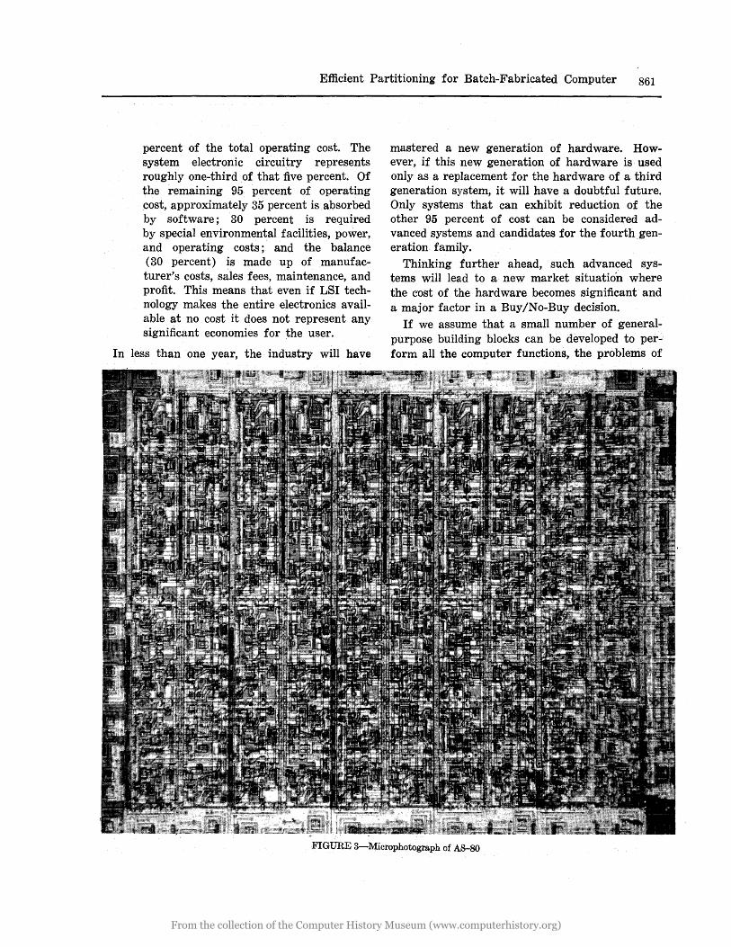
Interface with the AS-SO is at standard Transistor-Transistor-Logic (TTL) levels. Input and output characteristics are identical to those published for high level TTL circuits. Gate outputs designed to be used internally on the chip can be c'Onnected t'Ogether t'O form wired OR functi'Ons. The AS-SO array is currently fabricated by Sylvania 'On a single monolithic "chip" with three levels 'Of metallization f'Or the internal connecti'Ons. Figure 3 is the microphotograph of an area of a silicon slice where an AS-SO is formed. On the periphery the b'Onding pads are also visible.
Arithmetic operations require the use of an'Other logic element. A highly c'Omplex f'Our-bit array was designed which perf'Orms most arithmetic and logic combinations 'Of two operands, and can be implemented with 70 gates and 24 pins. H'Owever, it functi'Onally 'Overlaps the AS-SO register array, and its usage is limited; theref'Ore, its building block usefulness is questionable.
Examination of the AS-SO array shows that many of the functions of a general arithmetic unit are included in the array (shift, complements, count, etc.). All that is necessary in the arithmetic unit are the pure add (and therefore subtract) 'Operations associated with a central processor. Selection gating provided at one of the operand inputs 'Of the register array enables c'Onvenient implementation of subtraction. In addition to the r,egister and adder arrays, control logic is required to provide synchronization, gating . signals, and a sequence. of I'Ogic instructions in order t'O be operated as a homogene'Ous system.
2) Register Array Concept for the Fourth Generation (RAGON-h-) Every system previ'Ously described had t'O carry the burden 'Of third generation computer 'Operation, such as specialized hardware, high applicati'On programming cost, and excessive processing time for internal scheduling (Reference 3).
Users 'Of third generation systems have found that in the case 'Of leased equipment, the cost of hardware is only about five
....,
"I FZ F'I o 0 0 C.t..~""R o 0 I "Hln u:JC"T
o I 0 S",'F'T R\~"''T o , '\.O""t) 1&0.
I 0 0 HO\..O I , 0 c.ou ... .,. t::IC)y,(W
I \ I COUNT VP I 0 , CQMP\.SMs,,,,,'T
\.. t..N-4 8E."CQ~D WIT", 1IfrroN"( 0'- "'8C)"" TO \..0""0 -:v c::A ~ IIt.\..()N£J ~C\.u..R C.ODE
~£RO DETECT c::Jtoo4 F'1:Q1 A."f ON" Dl.T~c.."T O ..... ~I)t.ou'T
FIGURE 2-Logic schematic of AS-SO
From the collection of the Computer History Museum (www.computerhistory.org)
Efficient Partitioning for Batch-Fabricated Computer 861
percent of the total operating cost. The system electronic circuitry represents roughly one-third of that five percent. Of the remaining 95 percent of operating cost, approximately 35 percent is absorbed by software; 30 percent is required by special environmental facilities, power, and operating costs; and the balance (30 percent) is made up of manufacturer's costs, sales fees, maintenance, and profit. This means that even if LSI technology makes the entire electronics available at no cost it does not represent any significant economies for the user.
In less than one year, the industry will have
mastered a new generation of hardware. However, if this new generation of hardware is used only as a replacement for the hardware of a third generation system, it will have a doubtful future. Only systems that can exhibit reduction of the other 95 percent of cost can be considered advanced systems and candidates for the fourthgeneration family.
Thinking further ahead, such advanced systems will lead to a new market situation where the cost of the hardware becomes significant and a major factor in a Buy/No-Buy decision.
If we assume that a small number of generalpurpose building blocks can be developed to perform all the computer functions, the problems of
FIGURE 3-Microphotogra.ph of A8-80
From the collection of the Computer History Museum (www.computerhistory.org)
862 Fall Joint Computer Conference, 1968
specialized hardware, of general-purpose capabilities where only specialized functions are required, of excessive programming costs, and of prohibi~ tive processing times would be solved for both user and manufacturer. The producer of computing machines would build up an inventory of these basic blocks and assemble them to the size and configuration of the user's requirements with a minimum of system design effort. Computing systems will then be defined by the total number of bits of all working registers, rather than by the number and the size of registers. Fixed hardware implemented blocks will "personalize" the system. The user, on the other hand, will not be forced to buy capacity and features he does not need and the cost would become linearly proportional to the size and computing power required.
With this concept in mind, the current and future computing systems can be characterized as: .
• Third generation: Specialized hardware, General-purpose systems
• Fourth generation: Specialized systems, General-purpose hardware
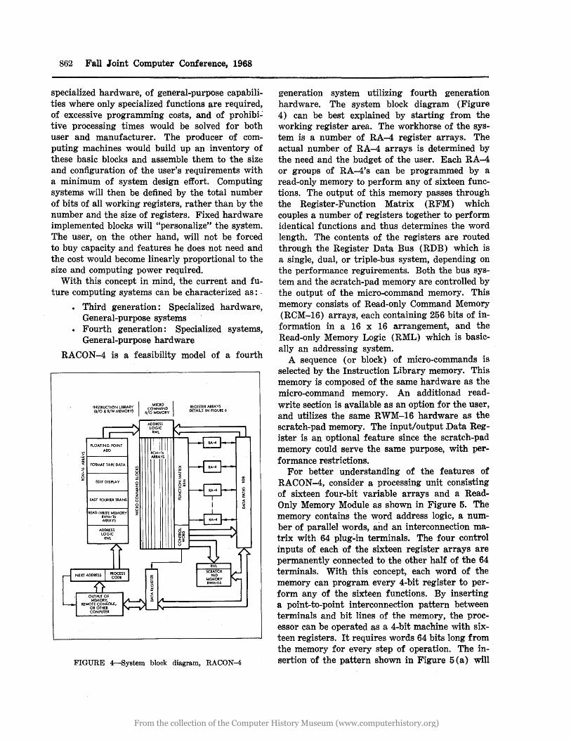
RACON-4 is a feasibility model of a fourth
INSTRUCTION LIBRARY MICRO I (R!O & R/W MEMORy) Jg~~~~y
~
'i ~F-OR-MA-T T-APE-D-ATA-I
~I------I ~
EDIT DISPlAY
FAST FOURIER TRANS
READ-WRITE MEMORY RWM-16 ARRAYS
REGISTER ARRAYS DETAILS IN FIGURE 6
FIGURE 4-System block diagram, RACON-4
generation system utilizing fourth generation hardware. The system block diagram (Figure 4) can be best explained by starting from the working register area. The workhorse of the system is a number of RA-4 register arrays. The actual number of RA-4 arrays is determined by the need and the budget of the user. Each RA-4 or groups of RA-4's can be programmed by a read-only memory to perform any of sixteen functions. The output of this memory passes through the Register-Function Matrix (RFM) which couples a number of registers together to perform identical functions and thus determines the word length. The contents of the registers are routed through the Register Data Bus (RDB) which is a single, dual, or triple-bus system, depending on the performance regriirements. Both the bus system and the scratch-pad memory are controlled by the output of the micro-command memory. This memory consists of Read-only Command Memory (RCM-16) arrays, each containing 256 bits of information in a 16 x 16 arrangement, and the Read-only Memory Logic (RML) which is basically an addressing system.
A sequence (or block) of micro-commands is selected by the Instruction Library memory. This memory is composed of the same hardware as the micro-command memory. An additionad readwrite section is available as an option for the user, and utilizes the same RWM-16 hardware as the scratch-pad memory. The input/output .Data Register is an optional feature since the scratch-pad memory could serve the same purpose, with performance restrictions.
For better understanding of the features of RACON-4, consider a processing unit consisting of sixteen four-bit variable arrays and a ReadOnly Memory Module as shown in Figure 5. The memory contains the word address logic, a number of parallel words, and an interconnection matrix with 64 plug':'in terminals. The four control inputs of each of the sixteen register arrays are permanently connected to the other half of the 64 terminals. With this concept, each word of the memory can program. every 4-hit register to perform any of the sixteen functions. By inserting a point-to-point interconnection pattern between terminals and bit lines of the memory, the processor can be operated as a 4-bit machine with sixteen registers. It requires words 64 bits long from the memory for every step of operation. The insertion of the pattern shown in Figure 5 (a) will
From the collection of the Computer History Museum (www.computerhistory.org)
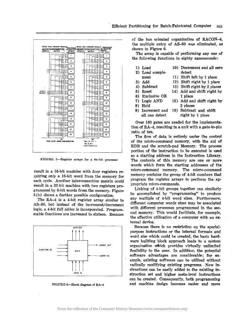
Efficient Partitioning for Batch-Fabricated Computer 863
MEMORY ARRAYS
6 BIT I W ORDS
INTERCONNECTION MATRIX
~ I--C
1--=
~ I--l=~ I--t:::~
m r--l=~ - r=~
~ r--- ~ !-
~
(A)
~ ~~~
FOUl 16 BIT -WORD CONFIGlI!ATION (B)
TWO 24 BIT + TWO B BIT CONFIGURATION
FIGURE 5-Register arrays for. a 64-bit processor
result in a 16-bit machine with four registers requiring only a 16-bit word from the memory for each cycle. Another interconnection matrix could result in a 32-bit machine with two registers programmed by 6-bit words from the memory. Figure 5 (b) shows a further possible configuration.
The RA-4 is a 4-bit register array similar to AS-80, but instead of the increment/decrement logic, a 4-bit full adder is incorporated. Programmable functions' are increased to sixteen. Because
DATA OUT
CARRY OUT
FUNCTION IN RA-4
CARRY 'IN
DATA !N
FIGURE 6-Block diagram of RA-4
of the bus 'Oriented organization of RACON-4, the multiple entry of AS-80 was eliminated, as shown in Figure 6.
The array is capable of performing anyone of the following functions in eighty nanoseconds:
1) Load 10) Decrement and all zero 2) Load comple- detect
ment 11) Shift left by 1 place 3) Add 12) Shift right by 1 place 4) Subtract 13) Shift right by 2 places 5) Reset 14) Add and shift right by 6) Exclusive OR 1 place 7) Logic AND 15) Add and shift right by· 8) Hold 2 places 9) Increment and 16) Subtract and shift
all one detect right by 1 place
Over 160 gates are needed for the implementation of RA-4, resulting in a unit with a gate-to-pin ratio of ten.
The flow of data is entirely under the control 'Of the micro-command memory, with the aid of RDB and the scratch-pad Memory. The process portion of the instruction to be executed is used as a starting address in the Instruction Library. The contents of this memory are one or more words which f'Orm the starting addresses of the micro-command memory. The micro-command memory contains the group of 4-bit numbers that program the register arrays to perform the ap~ propriate micro-c'Ommands.
Linking of 4-bit groups together can similarly be accomplished by "programming" to produce any multiple of 4-bit word sizes. Furtherm'Ore, different computer words sizes may be associated with different processes programmed in the second memory. This would facilitate, for example, the effective utilization of a computer with an external device.
Because there is no restricti'on on the specialpurpose instructions or the internal formats and word size which could be created, the basic hardware building block approach leads to a system organization Which provides virtually unlimited flexibility to the user. In addition, the p'Otential software advantages are considerable; for example, ·existing software can be utilized without radically modifying existing pragrams. New instructions can be easily added to the existing instruction set and higher meta-level instructions can be created. Consequently, both programming and machine design bec'Omes easier and more
From the collection of the Computer History Museum (www.computerhistory.org)
.864 Fall Joint Computer Conference, 1968
adaptable to any application. without any loss in generality .
The entire control system, consisting of all control algorithms and computer instructions, can be represented by programmed blocks 'Of fundamental machine operations placed in the microcommand memory. This approach differs from the micro-programmed computers in which specific computer functions are prpgrammed, or from a standard computer in which specifi<} functions are hardwired. Instead of d~~ignating special registers (accumulators, count~rs, index registers, etc.) and parameters (transfets, invert, etc.) in each of these blocks of machine 'operation, a variable representation is used. Consequently, the blocks are general, so that each block can, with different register and parameter ~ designations, perform the functions of a large number of specific instructions.
Creating the entire set of computer instructions with these general micro-command blocks may be contrasted with present-day digital computer control memory techniques. In today's computers, the instruction complement consists of a. collection 'Of special-purpose instructions which differ slightly in terms of processes; there are many different instructions, but only a few unique operations. U sing the general micro-command blocks as a basis, any desired set of instructions can be defined.
In fact, different sets of blocks can. be specified to effect different system characteristics, depending upon the application. A representative ~et of blocks forming a complete (and powerful) instruction complement is listed below, together with the· specific instructions accomplished within the block:
1) Transfer: This block implements the operations of transfer, enter, execute, singlebit tests, etc.
2) Count: This block implements the count (increment or decreme,nt).
3) Shift: This block implements all forms 'Of single . precision/double precision left/ right, open/closed, algebraic/logical shifts.
4) Exchange: This block implements swaps between any two registers.
5) Logical: This block implements the logical operations such as "and", "or".
6) Sign and Magnitude Add-Subtracts: This block implements all 'Of the variations of
sign and magnitude addition and subtracti'On.
7) Mask test : This block implements the on/ off tests of fields, tests of any collection of bits, and indicator resets.
8) Three-way comparison: This block implements all three-way comparisons 'as well as two-way logical comparison tests.
9) Multiply Divide Iteration step: This block implements the basic process for fixed/ floating multiplication/division of fixed or variable length.
Because any register can be used by the microcommand block, arbitrary names for different registers are unnecessary. Because a register, such as an accumulator, has a definiti'On in terms of its use, it may be convenient to give a name to a register in which a specific function or pr~cess is generally performed.
As a direct consequence of the fact that the general forms define basic processes, they are independent of normal c'Omputer word characteristics, such as word size and internal field definitions. Registers, in application, may have different word sizes. Consider, for example~ the general form for a shift operation. A general shift operation is typically a set of the f'Ollowing operations:
1) Shift A n places and store in A. 2) Shift B n places and store in B. 3) Repeat steps 1 and 2 m times.
·4) Shift sign of A to sign of B.
In this routine, A and B represent registers, the parameter n represents the hardwired shift algorithm, and the parameter m represents the number of times the shift algorithm is used. Obviously Steps 1 and 2, used together, represent a double precision shift; Step 1 alone is a single precisi'On shift.
It should be observed that A and B could be different length registers.
As a result of being able to program the basic control sequences in terms of primitive forms, only a small percentage of control logic remains to be implemented. Part of this logic, primarily the creation of more complex instructions, and the control logic required toestabIish internal formats, can also be handled by programming techniques.
Specialized processes consist of collections of the basic forms. The program to implement these
From the collection of the Computer History Museum (www.computerhistory.org)
Efficient Partitioning for Batch-Fabricated Computer 865
processes utilizes the "language" of the basic general forms. Consider the floating point operations; these are programmed by combining the basic forms. A "floating add" is a collection of "transfer," "logical," "exchange," "shift," and "sign and magnitude" subroutines. "Floating subtract" is the same as "floating add" after the first subroutine, a sign change. This is analogous to the manner in which the control of complex computer instructions is presently achieved in computer design (built-in subroutines with specialized suborders). For example, the standard multiply instruction consists of 1) determining the sign of the answer, 2) the multipliS!ation process of add, shift, and iterate, and 3) the final adjustment of the answer.
The programming of these specialized processes is performed in a second read-only memory called the instruction library. The ability to program this memory, using the general building block forms in the micro-command memory as a source language, allows functions normally ascribed to the software to be built into the hardware by being programmed in the instruction library. Thus specialized instructions can be created and special-
. i~ed routines for which high processing speed is required, such as input/output mechanizations (reading and writing data, editing procedures, input/output buffer control) or a Fast Fourier Transform algorithm, can be implemented in add i-
tional to normal computer instructions. This approach permits the computer to be tai
lored for many specific applications within the mass-produced standard computer design without the need for specialized software. Much of the complexity of a higher order language is bypassed.
CONCLUSION
Recent developments in batch fabrication of logic and memories have made it necessary to reconsider the interrelations between design effort, hardware cost, and partitioning. It is possible to achieve a low "part-number" count by making use of multipurpose register array packages that include control logic inputs. These control inputs are supplied from read-only memories. The control inputs cause th~ data in the package to undergo microprogrammed operations to form the instructions of the computer.
REFERENCES
1 R C JENNINGS Design and fabrication oj a general-purpose. airborne computer using LSI arrays Digest of IEEE Computer Group Conference June 1968
2 H R BEELITZ et al System architecture for large-scale integration Proceedings of Fall Joint Computer Conference 1967
3 CJWALTER Impact offourth generation software on hardware design IEEE Computer Group News July 1968
From the collection of the Computer History Museum (www.computerhistory.org)

From the collection of the Computer History Museum (www.computerhistory.org)