efficient handling of operating range and...
TRANSCRIPT

IEEE TRANSACTIONS ON COMPUTER AIDED DESIGN OF INTEGRATRATED CIRCUITS AND SYSTEMS, VOL. 19, NO. 8, AUGUST 2000 825
Efficient Handling of Operating Range andManufacturing Line Variations in Analog Cell
SynthesisTamal Mukherjee, Member, IEEE, L. Richard Carley, Fellow, IEEE, and Rob A. Rutenbar, Fellow, IEEE
Abstract—We describe a synthesis system that takes operatingrange constraints and inter and intracircuit parametric manufac-turing variations into account while designing a sized and biasedanalog circuit. Previous approaches to computer-aided design foranalog circuit synthesis have concentrated on nominal analog cir-cuit design, and subsequent optimization of these circuits for sta-tistical fluctuations and operating point ranges. Our approach si-multaneously synthesizes and optimizes for operating and manu-facturing variations by mapping the circuit design problem into anInfinite Programming problem and solving it using an annealingwithin annealing formulation. We present circuits designed by thisintegrated synthesis system, and show that they indeed meet theiroperating range and parametric manufacturing constraints. Andfinally, we show that our consideration of variations during theinitial optimization-based circuit synthesis leads to better startingpoints for post-synthesis yield optimization than a classical nom-inal synthesis approach.
I. INTRODUCTION
A LTHOUGH one-fifth the size of the digital integratedcircuit (IC) market, mixed-signal IC’s represent one of the
fastest-growing segments of the semiconductor industry. Thiscontinuing integration of analog functionality into traditionallydigital application-specific ICs (ASIC’s) coupled with thetime-to-market pressures in this segment of the semiconductorindustry has demanded increasing amounts of support fromdesign automation tools and methodologies. While digitalcomputer-aided design tools have supported the rapid transitionof design ideas into silicon for a generation of designers, theanalog portion of the mixed-signal IC, although small in size,is still typically designed by hand [1], [2].
A wide range of methodologies has emerged to design thesecircuits [3]. These methodologies start withcircuit synthesisfol-lowed bycircuit layout. This paper focuses on thecircuit syn-thesisportion, in which performance specifications are trans-lated into a schematic with sized transistors, a process involvingtopology selection as well as device sizing and biasing. Existingapproaches tend to synthesize circuits considering only a nom-inal operating point and a nominal process point. At best, ex-isting approaches allow the expert synthesis tool creator to pres-
Manuscript received July 22, 1998; revised August 23, 1999. This work wassupported in part by the Semiconductor Research Corporation (SRC) underContract DC 068. This paper was recommended by Associate Editor M. Sar-rafzadeh.
The authors are with the Electrical and Computer Engineering Department,Carnegie Mellon University, Pittsburgh, PA 15213 USA.
Publisher Item Identifier S 0278-0070(00)06421-6.
Fig. 1. Variation of dc gain of manual and synthesized design withV .
elect specific operating and process points for performance eval-uation.
Because ICs are sensitive to parametric fluctuations inthe manufacturing process, design with a nominal set ofmanufacturing process parameters is insufficient. In addition,all circuits are sensitive to fluctuations in their operatingconditions (e.g., power supply voltages and temperature). Theimportance of these variations leads to the two phase approachcommon in manual design: first, generate a nominal designusing topologies known to be relatively tolerant of operatingrange and parametric manufacturing variations, then improvethe design’s manufacturablility using worst case methods.
An automated circuit design flow that combines analog cir-cuit synthesis for nominal design and yield optimization formanufacturability can mimic this manual approach. The goalof analog circuit synthesis tools is to decrease design time. Thegoal of yield optimization tools is to improve the manufactura-bility of an already well-designed circuit. While both sets oftools are aimed at helping the designer, they both solve half theproblem. Synthesis tools often create designs that are at the edgeof the performance space, whereas a good human designer usinga familiar topology can conservatively over-design to ensure ad-equate yield. We have empirically observed that yield optimiza-tion tools can improve the yields of good manual designs, butautomatically synthesized circuits are often a bad starting pointfor gradient-based post-synthesis yield optimization.
Two examples make these issues concrete. Fig. 1 shows theimpact of variation in a single environmental operating pointvariable on a small CMOS amplifier design. The variable is thesupply voltage, , which has a nominal value of 5.0 V. Fig. 1plots the dc gain performance over varying supply voltage for
0278–0070/00$10.00 © 2000 IEEE

826 IEEE TRANSACTIONS ON COMPUTER AIDED DESIGN OF INTEGRATRATED CIRCUITS AND SYSTEMS, VOL. 19, NO. 8, AUGUST 2000
Fig. 2. Effect of manufacturing variation on circuit performance.
Fig. 3. Post-design yield optimization on manual and nominal designs.
two designs: one done manually, one done using synthesis [4].Both designs meet the nominal specification of 70 dB of gainat 5.0 V, but the synthetic design shows large sensitivity to evensmall changes in . (One reason in this particular design istoo many devices biased too close to the edge of saturation.)Fig. 2 shows the impact of manufacturing variation on a secondsmall CMOS circuit. We consider here statistical variation injust one parameter: , the PMOS flat-band voltage, rangingover variation. Fig. 2 plots two performance parameters, dcgain (on left -axis) and output swing (on right-axis), and alsoshows curves for both a manual, and a synthesized [4] design.Again, both designs meet nominal specifications in the pres-ence of no variation, but the synthesized design showslarge sensitivities to any variation. Fig. 3 illustrates an attemptto use post-design statistical yield maximization on the two de-signs from Fig. 2. The figure plots circuit yield, determined viaMonte Carlo analysis, after each iteration of a gradient-basedyield optimization algorithm [5]. It can be seen that the manualdesign ramps quickly from 75% to near 100% estimated yield.However, the synthetic design makes no progress at all; its yieldgradients are all essentially zero, locating this design in an in-escapable local minimum.
Our goal in this paper is to address this specific problem: howto avoid nominal analog synthesis solutions that are so sensitiveto operating/manufacturing variation that they defeat subsequentoptimization attempts. To do this, we add simplified models ofoperating point and manufacturing variation to the nominal syn-thesis process. It is worth noting explicitly that we do not proposeto obsolete post-design statistical optimization techniques. Ouraimisnottocreate, inasinglenumericalsearch,a“perfect”circuitwhich meets all specifications and is immune to all variation.Rather, the goal is the practical one ofmanagingthe sensitivity tovariationof thesesynthesizedcircuits,so that theyarecompatiblewithexistingpost-designyieldoptimization.
We achieve this goal by developing a unified framework inwhich interchip and intrachip parametric fluctuations in the fab-rication process, environmental operating point fluctuations, andthebasicnumericalsearchprocessofsizingandbiasingananalogcell are all dealt withconcurrently.We show how the problemcanbe formulated by adapting ideas from Infinite Programming [6],and solved practically for analog cells using simulated annealing[7] for the required nonlinear optimizations. An early versionof these ideas appeared in [8]. As far as we are aware, this is thefirst full circuit synthesis formulationwhich treats bothoperatingand manufacturing variations, and the first application of infiniteprogrammingtothissynthesis task.
The remainder of the paper is organized as follows. Sec-tion II reviews prior analog circuit synthesis approaches, withemphasis on the nominal synthesis approach that is our ownnumerical starting point. Section III shows how operating andmanufacturing variations can be simplified so as to allow aunified treatment of these as constraints using a basic infiniteprogramming formulation. Section IV introduces a highlysimplified, idealized infinite programming algorithm, whichallows us to highlight critical points of concern in problemsof this type. Section V then develops a practical algorithmfor application to analog synthesis, and also highlights theheuristics we employ when the assumptions that underlythe idealized infinite programming algorithm are no longervalid. Section VI offers a variety of experimental synthesisresults from a working implementation of these ideas. Finally,Section VII offers concluding remarks.

MUKHERJEEet al.: EFFICIENT HANDLING OF OPERATING RANGE AND MANUFACTURING LINE VARIATIONS 827
II. REVIEW OF ANALOG CIRCUIT SYNTHESIS
The advent of computer-based circuit simulation led to thefirst studies of computer-based circuit design, e.g., [9]. Sincethen, a variety of circuit synthesis approaches have been devel-oped that range from solving both the topology selection anddevice sizing/biasing problems simultaneously [10] to solvingthem in tandem; from using circuit simulators for evaluating cir-cuit performance [11], to behavioral equations predicting cir-cuit performance [12], [13]; from searching the design spacewith optimization [14], [15], to using a set of inverted behav-ioral equations with a restricted search space [1]. See [3] for arecent survey of analog circuit synthesis.
The system presented in this paper is based onASTRX/OBLX [4], which first translates the design probleminto a cost function whose minimum is carefully crafted to bethe best solution to the design problem, and then minimizesthis cost function to synthesize the required circuit. It has beensuccessful at designing the widest range of analog circuitsto date [4], [16]–[18]. The key ideas in the ASTRX/OBLXsynthesis strategy are summarized below:
• Automatic Compilation: ASTRX compiles the inputcircuit design into a performance prediction module thatmaps the circuit component parameters (such as devicelengths and widths) to the performance metrics (suchas the circuit’s dc gain) specified by the designer. If thedesigner specifies an equation for the circuit performancemetric as a function of the component parameters, themapping is trivial. For the remaining performance met-rics, ASTRX links to the device modeling and circuitevaluation approaches below to create a cost function,or single metric that indicates how well the currentcomponent parameters can meet the circuit design goalsand specifications.
• Synthesis via Optimization: The circuit synthesisproblem is mapped onto a constrained optimizationformulation that is solved in an unconstrained fashion, aswill be detailed below.
• Device Modeling via Encapsulation:A compiled data-base of industrial models for active devices is used to pro-vide the accuracy of a general-purpose circuit simulator,while making the synthesis tool independent of low-levelmodeling concerns [4], [19]. The results presented in thispaper use the BSIM1 model from this library.
• Circuit Evaluation by Model Order Reduction:Asymptotic waveform evaluation (AWE) [20] is aug-mented with some simple, automatically generatedanalytical analyses to convert AWE transfer functionsinto circuit performances. AWE is a robust, efficient ap-proach to analysis of arbitrary linear RLC circuits that formany applications is several orders of magnitude fasterthan SPICE. The circuit being synthesized is linearized,and AWE is used for all linear circuit performanceevaluation.
• Efficiency via Relaxed-dc numerical formulation: Ef-ficiency is gained by avoiding a CPU-intensive dc oper-ating point solution after each perturbation of the circuitdesign variables [4], [19]. Since encapsulated models must
be treated numerically, as in circuit simulation, an iterativealgorithm such as Newton Raphson is required to solvefor the nodal voltages required to ensure the circuit obeysKirchhoff’s Current Law. For synthesis, Kirchhoff’s Cur-rent Law is implicitly solved as an optimization goal byadding the list of nodal variables to the list of circuit designvariables. Just as optimization goals are formulated, suchas meeting gain or bandwidth constraints, now dc-correct-ness is formulated as yet another goal that needs to be met.
• Solution by Simulated Annealing:The optimization en-gine which drives the search for a circuit solution is sim-ulated annealing [7]; it provides robustness and the po-tential for global optimization in the face of many localminima. Because annealing incorporates controlledhill-climbing it can escape local minima and is essentiallystarting-point independent. Annealing also has other ap-pealing properties including: the inherent robustness of thealgorithm in the face of discontinuous cost functions, andthe ability to optimize without derivatives, both of whichare taken advantage of later in this paper.
Two of these ideas are particularly pertinent to our implemen-tation (which will be described in Section V), and are reviewedin more detail. They include the optimization formulation, andthe use of simulated annealing for solving the optimizationproblem. Our work extends thissynthesis-via-optimizationformulation. In ASTRX/OBLX, the synthesis problem ismapped onto a constrained optimization formulation that issolved in an unconstrained fashion. As in [10], [11], and[14], the circuit design problem is mapped to the nonlinearconstrained optimization problem (NLP) of (1), where isthevector of independent variables—geometries of semiconductordevices or values of passive circuit components—that arechanged to determine circuit performance; is a set ofobjective functions that codify performance specifications thedesigner wishes to optimize, e.g., area or power; andis a set of constraint functions that codify specifications thatmust be beyond a specific goal, e.g., 60 dB- .Scalar weights, , balance competing objectives. The decisionvariables can be described as a set , where is the setof allowable values for
NLP (1)
To allow the use of simulated annealing, in ASTRX/OBLXthis constrained optimization problem is converted to an uncon-strained optimization problem with the use of additional scalarweights (assumingconstraint functions)
(2)
As a result, the goal becomes minimization of a scalar costfunction, , defined by (2). The key to this formulation isthat the minimum of corresponds to the circuit design that

828 IEEE TRANSACTIONS ON COMPUTER AIDED DESIGN OF INTEGRATRATED CIRCUITS AND SYSTEMS, VOL. 19, NO. 8, AUGUST 2000
best matches the given specifications. Thus, the synthesis taskis divided into two subtasks: evaluating and searching forits minimum.
In the next section, we will revisit the general NLP optimiza-tion formulation of (1) with the aim of extending it to handleoperating range and manufacturing line variations. Then, in Sec-tion V we will revisit the unconstrained formulation of (2) usedin ASTRX/OBLX, when we discuss our annealing-based im-plementation.
III. I NFINITE PROGRAMMING APPROACH TOANALOG CIRCUIT
SYNTHESIS
In this section we will expand the nonlinear constrained opti-mization formulation in ASTRX/OBLX to a nonlinear infiniteprogramming formulation that considers operating range andparametric manufacturing variations. Our goal for this formula-tion is a complete model of the design problem, thereby solvingthe operating point and manufacturing variations in a unifiedmanner. A complete model is required in order to use an op-timization-based synthesis algorithm; partially modeled prob-lems ignore practical constraints, hence, they let the optimiza-tion have freedom to search in areas that lead to impractical de-signs. The resulting unified formulation simultaneously synthe-sizes a circuit while handling the two independent variations.
IC designers often guess worst case range limits from expe-rience for use during the initial design phase. Once they havegenerated a sized schematic for the nominal operating point (i.e.,bias, temperature) and process parameters, they test their designacross a wide range of process and operating points (worst caseset). Typically, the initial design meets specifications at severalworst case points, but needs to be modified to ensure that thespecifications are met at the rest of the worst case points. Wewill now first consider the types of worst case points found incircuits before proposing a representation that mathematicallymodels them.
Let us begin with a typical example of an environmental oper-ating point specification: the circuit power supply voltage,.Most designs have a 10% range specification on the powersupply voltage, leading to an operating rangeV in a 5-V process. Graphs similar to the one shown in Fig. 1for the performances in many analog circuits (from simulation,as well as from data books) show the following.
• Low designs are the ones most likely to fail to meet theperformance specifications, so there is a need to considerthe additional worst case point of 4.5 V in themathematical program used to design the circuit.
• Not all of the performance parameters are monotonicfunctions of the operating point. Therefore, a mechanismto find the worst case point in the operating range foreach performance function is needed. Even when theperformance parameters are monotonic functions of theoperating point, a mechanism to determine the worst casecorner is needed since this corner may not bea prioriknown.
To investigate the effect of introducing operating ranges tothe NLP model of (1), let us consider the example of dc gain,acircuit performance metric, and the power supply voltage range,
anoperating range: the dc gain needs to be larger than 60 dB forevery power supply voltage value in the range .This can be written as in (1), whereis the vector of designableparameters, and is a new variable (in this example only ascalar), to represent the operating range
(3)
where is considered to be arange variable.Since every single voltage in the given range needs to be
investigated, this single operating range constraint adds aninfinite number of constraints to the mathematical program.Heittich, Fiacco, and Kortanek present several papers in [6],[21] which discuss nonlinear optimization problems wheresome constraints need to hold for a given range of an operatingrange variable. These problems, and the one just presented,are calledsemi-infinite programsdue to their finite number ofobjectives and infinite number of constraints. When there is aninfinite number of objective functions (due to the presence ofa range variable in the objective function), the mathematicalprogram is called aninfinite program. The complete mathe-matical program can now be re-written as thenonlinear infiniteprogram(NLIP) shown in (4) where is the vector set of op-erating point ranges and statistical manufacturing fluctuations
NLIP (4)
Equation (4) reduces into the NLP formulation of (1) if the rangevariables are considered to be fixed at their nominal values (thisis how ASTRX/OBLX solves the nominal synthesis problem).
So, we can see that environmental operating point variablesthat can vary over a continuous range can be incorporateddirectly into this nonlinear infinite programming formulation.However, for statistical fluctuations, such as those character-izing the manufacturing process, this formulation cannot beused directly. We need some suitable transformation of thesestatistical variations to treat them as in (4).
Consider how designers empirically deal with statisticalprocess variations in manual circuit design. Once the circuitmeets the performance specifications at a few token worstcase points, the designer begins improving the circuit’s yieldby statistical design techniques [22]–[25]. Some of thesetechniques also include operating ranges [26], [27]. Such yieldmaximization algorithms can be used to determine the bestdesign for a given set of specifications and a joint probabilitydistribution of the fluctuations in the fabrication line. Ourunified formulation attacks the problem of manufacturing linefluctuations, but in a different way than the yield maximizationapproach. Specifically, we convert the statistical variationproblem into a range problem. This critical simplificationallows us to treat both operating range variation and statisticalmanufacturing variation in a unified fashion.

MUKHERJEEet al.: EFFICIENT HANDLING OF OPERATING RANGE AND MANUFACTURING LINE VARIATIONS 829
Fig. 4. Contours of jpdf of fabrication line model.
It has been shown that relatively few device model variablescapture the bulk of the variations in a MOS manufacturingline [28], [29], with the most significant ones being thresholdvoltage, oxide thickness and the length and width lithographicvariations. In practice, the oxide thickness variation is verytightly controlled in modern processes. In addition, for analogcells, the devices widths are much larger than the lengths.Therefore, the circuit performances will be more sensitiveto length variations than to width variations. Therefore, twosources of variation, intrachip threshold voltage variation,and intrachip length reduction variation, dominate mostanalog designs. is the difference in the threshold voltagebetween two identical devices on the same chip. is thedifference in the lengths of the identical devices on the samechip. This limited number of range variables is crucial to therun times of our approach, as we shall see later. To explainour modeling approach, let us consider an example where theremaining parameters do not vary.
What we want is a model of the fabrication line that allowsus to determine sensible ranges for the constraints on and
. While a simple strategy is to use the wafer acceptance spec-ifications provided by the process engineers, we will considera joint-probability distribution function (jpdf) that a fabricatedchip has an intrachip threshold voltage difference of andan intrachip length difference of : . This willhelp in comparing and contrasting with the approaches previ-ously used for yield optimization. This jpdf can be determinedusing measurements from test-circuits fabricated in the manu-facturing line or via statistical process and device simulation[30]. We can draw the contours of as shown inFig. 4 with the contour highlighted. In our model of the fab-rication line variations, we will treat this contour in exactly thesame way as a range variable. We, therefore, specify that thecircuit being designed should work for every possible value of
and within the contour. More exactly, we are con-straining the yield to be at least .
Stepping back from this specific example to consider the gen-eral approach, we see that this isnot a statistical IC design for-mulation of the synthesis problem. Instead it is a unified formu-lation that converts the problem of manufacturing line variationsinto the same numerical form as the operating range variations.We do this by converting these statistical fluctuations into a
range variable which spans asufficiently probablerange of thesestatistical distributions. Our formulation in (4) reduces to thefixed tolerance problem (FTP) of [31] if we only consider onlythe design objectives (and ignore the design constraints), and ifwe replace each objective with the maximum in the range space.An alternative approach, followed by [32] considers the integralof the objective over the jpdf (a metric for yield) by discretizingit into a summation, and approximating the continuous jpdf withdiscrete probabilities. Such an approach more correctly weightsthe objective with the correct probabilities of the range variablecapturing the manufacturing variation, but prevents the develop-ment of the unified approach. A unified approach is pursued inthis work to let the optimization simultaneously handle all theconstraints, thereby having a full model of the design problem.However, the price here is the simplified range model we mustuse for statistical variation.
We have shown how we can represent both operatingrange variation and (with some simplification) statisticalmanufacturing variation as constraints in a nonlinear infiniteprogramming formulation for circuit synthesis. The nextproblem is how we might numerically solve such a formulation.This is discussed next.
IV. A CONCEPTUAL INFINITE PROGRAMMING ALGORITHM
In this section, we will review the solution of a simple non-linear infinite program. We begin with a simplified form of thenonlinear infinite program to illustrate all the critical points ofconcern. Only a single design variable, and a single range vari-able are considered. Also, only a single objective, and a singleconstraint are considered, and functionsand are assumed tobe convex and continuous and the setis assumed to be convex.So, the problem is
(5)
In this problem, a point is feasible if (as a functionof ) is less or equal to zero on thewholeof . If is a finiteset, then , represents a finite number of in-equalities, and represents a finite number of objectives,the problem reduces to a common multiobjective nonlinear pro-gramming problem. On the other hand, ifis an infinite set (asin the case of a continuous variable), this problem is consid-ered to be aninfinite program.
Three existing approaches to solving this problem are nowoutlined. The first approach uses nondifferentiable optimiza-tion, while the second and third both use some discretizing ap-proximation of the initial infinite set , based on gridding andcutting planes.
In the first approach, thefor all term in the objective andconstraint are re-written into a nondifferentiable optimizationproblem. The infinite number of objectives can be replacedwith a single objective function as determined by the problem
. The objective now minimizes, in -space,the worst case value of the objective function (which is in-space). This approach is akin to the one followed for solving
multiobjective optimization problems. Similarly, the infinitenumber of constraints can be replaced by a single constraint

830 IEEE TRANSACTIONS ON COMPUTER AIDED DESIGN OF INTEGRATRATED CIRCUITS AND SYSTEMS, VOL. 19, NO. 8, AUGUST 2000
function as determined by the problem . Notethat the worst case value for is the maximum value in-space due to the direction of the inequality (a greater-than
inequality would lead to a minimization in-space). In essence,the infinite constraints have been replaced by a single worstcase constraint. Thus, the problem in (5) is equivalent to
(6)
The resulting objective and constraint are both no longer differ-entiable and can be solved by applying methods of nondifferen-tiable optimization [33].
A second approach to solving the original problem, (5), is toovercome the infinite nature of the setby discretizing it tocreate a finite, approximate set via gridding. The simplest ap-proach is to create a fine grid and, therefore, a large but finitenumber of objectives and constraints, and solve for the optimumusing standard nonlinear programming approaches. A more el-egant method is to create a coarse grid and solve a nonlinearprogram with a few constraints and objectives. Then, the infor-mation gained from this solution can be used to further refinethe grid in the region of -space where this is necessary [34].
Our solution approach is a derivative of the cutting plane-based discretization originally proposed by [35]. The startingpoint is, for simplicity, a semi-infinite program, as shown in(7). In addition to the assumptions leading to (5), only a single(finite) objective is considered. We call thisProblem , and willrefer back to this as we develop the conceptual algorithm
(7)
A more detailed discussion of the cutting plane-based dis-cretization is presented to introduce notation needed for the an-nealing-within-annealing formulation that will be described inSection V. The infinite set is replaced with a worst case con-straint. Since we are trying to ensure that ,theworst caseor critical point is the maximum value of withrespect to , as shown in Fig. 5. If the constraint value at the crit-ical point is less than zero, then all points in-space will be lessthan zero, and the constraint due to the critical point is satisfiedfor the entire infinite set. Using this observation, we now breakthe infinite programming problem into two subproblems.
Let denote the problem
(8)
A simple conceptual algorithm begins with a andsolves
(9)
to obtain . Then, is computed by solving . Iffor , we are done. Note that since was
computed with the constraint , this constraint istrivially satisfied. Also, the critical point for is at ,
Fig. 5. The worst case point.
Fig. 6. Flow of conceptual cutting plane algorithm.
and if we meet the constraint at the critical point, we meetit within the entire range . So, if the inequality constraint
is met, we have met the constraint, and are atthe minimum value of the objective, implying we have solvedthe optimization problem, . If then we havenot met the constraint, and we have to go on to solve anothersubproblem
(10)
for , etc. The reason we consider both of the critical pointsand in is to ensure eventual convergence. The subscript inthe problem label indicates the iteration number. We can gener-alize this sequence of problems, labeled as, in which thereare only constraints; they can be written as
(11)
This sequence is interspersed with the problems with. The flow of this conceptual algorithm is, there-
fore, a sequence of two alternating optimization problems asshown in Fig. 6. Note that only has a finite number of con-straints. Therefore, we have been able to convert the semi-infi-nite programming problem into a sequence of finite nonlinearoptimization problems.
Each optimization, , adds a critical point, , resultingin a cutting plane , which reduces the feasible de-sign space to that of Problem, at which point the algorithmconverges to determine
(12)
where is any solution to Problem and is the objectivevalue of the problem .
This overall approach, alternating anouter optimizationwhich drives the basic design variables, with aninneroptimiza-tion, which adds critical points to approximating the infinite
MUKHERJEEet al.: EFFICIENT HANDLING OF OPERATING RANGE AND MANUFACTURING LINE VARIATIONS 831
Fig. 7. Complete conceptual algorithm for solving NLIP.
set . The above conceptual solution can be generalized tohandle more range variables and constraints, as well as to anobjective that is a function of range variables. Pseudocode forthe general algorithm appears in Fig. 7 where the setcontainsall the critical points determined by prior inner optimizations,
is identically (8) with the subscriptsince there are nowconstraints, and problem is a generalization
of (11) for multiple objective and constraint functions, which,for completeness, is
(13)
One of the problems of using this approach, like any other dis-cretization approach, is that asincreases, the number of con-straints in Problem increases, therefore, we need to considerremoving or pruning constraints for efficiency. This is often re-ferred to asconstraint-dropping. Eaves and Zangwill, in [35]show that under assumptions of convexity of the objective andconstraint functions and , the constraint can bedropped from Problem if:
• for the current solution , is larger than;
• ;• the next solution satisfies .
Intuitively, implies that an operating pointother than is contributing more significantly to the objectivethan which had led to the optimum . Also,means that the problem is feasible with thecritical point.Finally ensures that the feasible set isa subset of , satisfying (12). This constraint-droppingscheme suggests that the growth of complexity of Problemcan be slowed if the objective is nondecreasing.
This study of the conceptual algorithm has shown that a so-lution to the nonlinear infinite program is possible using a se-quence of alternating subproblems. These subproblems are fi-nite and can be solved by traditional optimization techniques.We have also seen that in the case of nondecreasing , thealgorithm will converge, and constraint dropping may be usedto improve the computational complexity of the algorithm.
Unfortunately, in our circuit synthesis application, the as-sumptions of convexity of either the objective function or thefeasibility region do not hold, thus, the convergence results suchas those in [6], [21], and [35] also cannot be guaranteed here.Nevertheless, we can still employ the basic algorithm of Fig. 7
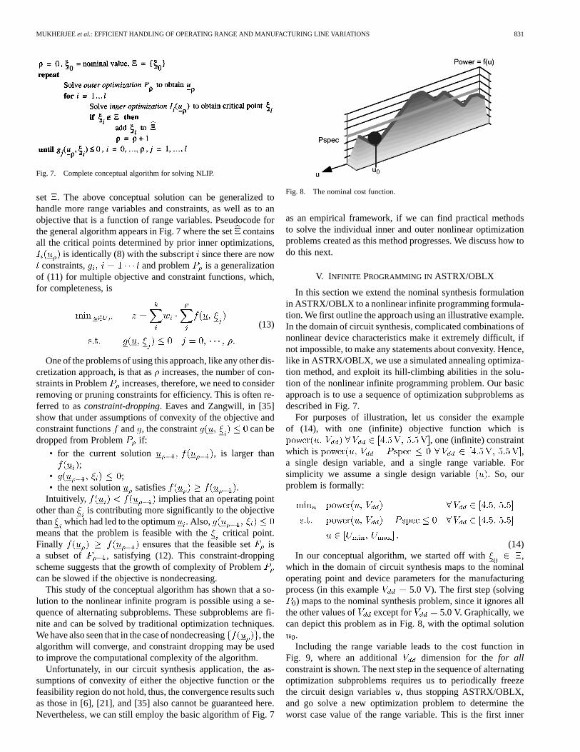
Fig. 8. The nominal cost function.
as an empirical framework, if we can find practical methodsto solve the individual inner and outer nonlinear optimizationproblems created as this method progresses. We discuss how todo this next.
V. INFINITE PROGRAMMING IN ASTRX/OBLX
In this section we extend the nominal synthesis formulationin ASTRX/OBLX to a nonlinear infinite programming formula-tion. We first outline the approach using an illustrative example.In the domain of circuit synthesis, complicated combinations ofnonlinear device characteristics make it extremely difficult, ifnot impossible, to make any statements about convexity. Hence,like in ASTRX/OBLX, we use a simulated annealing optimiza-tion method, and exploit its hill-climbing abilities in the solu-tion of the nonlinear infinite programming problem. Our basicapproach is to use a sequence of optimization subproblems asdescribed in Fig. 7.
For purposes of illustration, let us consider the exampleof (14), with one (infinite) objective function which is
, one (infinite) constraintwhich is ,a single design variable, and a single range variable. Forsimplicity we assume a single design variable . So, ourproblem is formally:
(14)In our conceptual algorithm, we started off with ,
which in the domain of circuit synthesis maps to the nominaloperating point and device parameters for the manufacturingprocess (in this example 5.0 V). The first step (solving
) maps to the nominal synthesis problem, since it ignores allthe other values of except for 5.0 V. Graphically, wecan depict this problem as in Fig. 8, with the optimal solution
.Including the range variable leads to the cost function in
Fig. 9, where an additional dimension for thefor allconstraint is shown. The next step in the sequence of alternatingoptimization subproblems requires us to periodically freezethe circuit design variables, thus stopping ASTRX/OBLX,and go solve a new optimization problem to determine theworst case value of the range variable. This is the first inner

832 IEEE TRANSACTIONS ON COMPUTER AIDED DESIGN OF INTEGRATRATED CIRCUITS AND SYSTEMS, VOL. 19, NO. 8, AUGUST 2000
Fig. 9. The meaning of8V 2 [4:5; 5:5].
Fig. 10. Inner optimization cost function.
optimization problem, whose cost function is describedin Fig. 10. The original outer optimization problem, , hadfound the minimum . We freeze the design variables at
and take the slice of ( as the costfunction for the inner optimization. Since we want to ensure that
, this corresponds to a maximization problem.If the maximum value of power in thecost function meets the specification, then all points across the
axis will meet the specification. Thus, the responsibility ofthe first inner optimization is to find the critical point, asin Fig. 11.
In the conceptual algorithm, the link back to the secondouter optimization involves adding another constraint tothe finite problem to create another finite optimizationproblem . Since ASTRX/OBLX solves the constrainedoptimization problem by converting it to an unconstrainedoptimization problem, the addition of is handled byaltering the ASTRX/OBLX cost function. The effect of addingthis information must modify the cost function of the outeroptimization in such a way to prevent it from searching aroundthe areas that are optimal in thenominalsense, but not in thefor all sense implied by the range variables. Fig. 12 shows thiseffect of adding the result of the inner optimization to the outeroptimization cost function for our simple example about circuitpower. The effect of this critical point is to make the originalouter optimization result suboptimal. Thus, we need tore-run the outer optimization on this new cost function. If the
Fig. 11. Solution of the inner optimization.
Fig. 12. Effect of inner optimization on outer optimization cost function.
inner optimization does not add any new critical points, thenthe outer optimization cost function remains the same, hence,no further outer optimizations are necessary.
We generate the second outer optimization cost functionshown on the right graph of Fig. 12 using the critical pointscollected so far: and . This cost function can bewritten as
(15)
The first term in the outer optimization cost function relates tothe discretization of the infinite objective. In the nominal case,we were trying to minimize , and now we are min-imizing the worst case value of the power at the discretizedpoints. The second and third terms relate to the discretizationof the infinite constraint. In the nominal cost function we haveonly one term for the constraint; now we have a term for everydiscretized value of . Solving this cost function, in terms ofASTRX/OBLX, is like designing a single circuit that is simul-taneously working at two different operating points,and . Equation (15) reduces to the nominal synthesis formu-lation in ASTRX/OBLX described in (2) if we assume that theonly possible value can take is .
Now let us consider implementing the inner/outer opti-mization approach in the ASTRX/OBLX framework. First,let us consider the direct approach. OBLX currently solvesthe problem , and can easily be extended to solve the outeroptimization problems . Each OBLX run takes from a fewminutes to a few hours, making it prohibitive to consider thisalternative. A possible second approach would be to iterateon the range space during every iteration of the designspace . In other words, after each perturbation in the current

MUKHERJEEet al.: EFFICIENT HANDLING OF OPERATING RANGE AND MANUFACTURING LINE VARIATIONS 833
Fig. 13. Annealing-within-annealing algorithm.
ASTRX/OBLX annealing-based approach, the inner optimiza-tions for each of the constraints, , will belaunched to update the list of critical points. Such a fine grainedinteraction between the inner and outer optimizations is alsonot reasonable. Note that each inner optimization involvesseveral iterations, or perturbations of therange variables;thus, we would have one nominal perturbation followed byseveral perturbations of the range variables, which is clearlyunbalanced. The circuit design variable space is the largerand more complicated space, hence, more effort should beexpended in determining the optimum in that space rather thandetermining more and more critical points.
Instead, we solve for the critical points in the middle of the an-nealing run, specifically, at each point when the annealing tem-perature related to the outer problem is reduced. This leads to asingle annealing run to solve all the outer optimization prob-lems (albeit slightly longer than simply solving the nom-inal synthesis problem, ). Inside this single annealing run, atevery change in the annealing temperature, the number of crit-ical points increases depending on the inner optimizations. Thisheuristic approach is the middle ground between solving theinner optimization problems at each per-turbation of the outer annealing problem , and solving theinner optimization between each annealing run as suggested bythe direct implementation of the conceptual scheme presented inthe previous section. Furthermore, empirical testing shows thatthis scheme tends to converge in a reasonable time period.
Given this overview, we can specify more precisely theoverall algorithm we employ. Fig. 13 gives pseudocode forthis annealing-in-annealing approach, in which the inner-op-timizations are performed at each temperature decrement inthe outer-optimization. The functionsfrozen, done_at_tem-perature, generate, acceptand update_tempare required forthe annealing algorithm and are detailed in [4] and [7]. Wefind empirically that these temperature decrement steps form anatural set of discrete stopping points in the outer optimizationswhich are numerous enough to update the critical points fre-
quently, but not so numerous as to overwhelm the actual circuitsynthesis process with critical-point-finding optimizations.
Although Fig. 13 gives the overall algorithm in its generalform, there are several practical observations which we canapply to reduce the overall amount of computation required.For example, Fig. 1 shows that it is not always necessary to doan inner optimization, since the function is often inpractice a one-dimensionally monotonic function of. Thus,the first part of the solution of should involve a test formonotonicity. We use a large-scale sensitivity computation todetermine monotonicity, and pick the appropriate corner of theoperating point and/or manufacturing range from there. Thistest can be applied to operating point variables which havebox constraints on them , where is thelower bound and is the upper bound for the dimensionin which is one dimensionally monotonic). Applyingsuch bounds to the statistical variables will lead to conservativedesigns. It will be left up to the user to tradeoff between ap-plying these bounds and getting conservative designs quickly,or actually doing an inner optimization over the space ofstatistical design variables to get a more aggressive design.
Constraint pruning or constraint dropping can also be em-ployed to reduce the total run times of the combined outer/inneroptimization. Recall that each inner optimization has the effectof indicating to the outer optimization that it should simultane-ously design the circuit for another value of the range variables.For the outer optimization, this means that each configurationperturbation (change in the design variables,) needs one morecomplete circuit simulation for each additional critical point.This is the primary source of growth in terms of run-time forthis approach. To control this growth in run-time, a critical pointpruning method can be applied. Unfortunately, in our nonconvexdomain, the Eaves and Zangwill [35] approach cannot work.
Instead, we consider dropping critical points using aleastrecentlyinactive heuristic. (Note in our conceptual discussionthere was a single inequality, so additional critical points addedjust one constraint, which is why it was calledconstraint drop-

834 IEEE TRANSACTIONS ON COMPUTER AIDED DESIGN OF INTEGRATRATED CIRCUITS AND SYSTEMS, VOL. 19, NO. 8, AUGUST 2000
ping by Eaves and Zangwill; in our problems the NLIP formu-lation has more than one constraint, so we prefer to use the termcritical point droppinginstead). During the early stages of theannealing, the Metropolis criterion encourages search across theentire design space, leading to the addition of several criticalpoints that are not useful during the later stages of more focusedsearching. Our approach is to collect statistics for each criticalpoint (each time the outer annealing decrements temperature) toindicate how often it is active. A critical point is considered to beactive if a constraint evaluated at the critical point for the currentdesign is violated. In the example of power minimization, wecan look at (15). Each time a critical point is active, itsfunction will return a positive number to increase the cost at thatdesign point. If the critical point is inactive, its functionreturns a zero, leaving the cost unaffected by that term. A criticalpoint becomes inactive when one of two situations occurs. Ei-ther another critical point has been added that is more strict thanthe inactive critical point, or the search in-space has evolvedto a region in this space where this critical point is no longeractive.
In either case, we can drop this inactive critical point withoutaffecting the cost function. There is a danger to doing this: thecritical point may become active at a later point. We, therefore,need to regularly check for this, which we do during each pertemperature iteration of the outer annealing. Therefore, our ap-proach is not to drop a critical pointcompletely, but rather tosuppressthe evaluation of the circuit at that critical point (hence,the critical point effectively does not contribute to the cost func-tion). This saves us the time-consuming component of the eachworst case point, the performance evaluation needed in eachouter perturbation. In addition, late in the annealing, we unsup-press all evaluations ensuring that the final answer will meet allthe critical points generated and will, therefore, be a synthesizedmanufacturable analog cell.
When the number of design constraints is large, critical pointstend to always remain active, since at least one of the design con-straints is active at each critical point. To overcome this, the totalcost function contribution of each critical point is computed ateach outer annealing temperature decrement. Critical points thatcontribute more than 15% (determined empirically) of the totalcost function are always evaluated, while those contributing lessare marked as inactive.
While various convergence proofs for the mathematical for-mulation of the infinite programming problem exist [6], [21],most require strict assumptions (e.g., linear constraint, convexobjective). The analog circuit synthesis problem, on the otherhand, tends to be highly nonlinear because of the mixture of dis-crete and continuous variables, our use of a penalty function forhandling the constraints in the annealing formulation, and theinherent nonlinearities in the transistor models. The example setof cross sections of an OBLX cost surface showing a myriad ofsharp peaks and valleys from [36] confirms that we cannot relyon any convexity assumptions.
Practical implementations of nondeterministic algorithmstend to have control parameters that are tuned to ensure qualitysolutions in the shortest amount of time. Our implementationof annealing uses the parameters determined in [4], with therun times for both the inner and outer annealing growing as
Fig. 14. An operational transconductance amplifier.
where is the number of synthesis variables for theouter annealer, and the number of range variables for the innerannealer. Of course, each of the evaluations of our costfunction is proportional to the number of critical points that areactive during the optimization, which can be an exponentialfunction of the number of range variables. As the number ofrange variables tends to be small, this exponential nature hasnot been observed to be a critical issue in our experiments.Furthermore, the constraint dropping scheme can control thisgrowth, as is shown in the results presented in Section VI.
VI. RESULTS
We applied the above annealing approach to solving the non-linear infinite programming formulation of the analog circuitsynthesis problem to a small operational transconductance am-plifier (OTA) cell, and to a large folded cascode amplifier cell.We compare these results with the original ASTRX/OBLX [4]designs to show that it is indeed important to take parametricmanufacturing variations and operating point variations into ac-count during analog circuit synthesis. In both circuits, we firstadded the operating range as the only worst case variableto consider. In addition, we also considered global variations intransistor geometries, global parametric variations in thresholdvoltages, and intrachip parametric variations in the thresholdvoltages of matched devices on the OTA to show that the NLIPformulation can incorporate both inter and intrachip statisticalfluctuations in the form of yield as a constraint.
Fig. 14 shows the Simple OTA circuit and the test-jig usedto simulate the circuit in HSPICE [37] for the results presentedbelow. There are six design variables: the width and length of thedifferential-pair transistors (M1 and M2), the width and lengthof the current mirror transistors (M3 and M4), the width andlength of the tail current source transistor (M5), and thevoltage. For the NLIP formulation, we added the operatingpoint variable as a worst case variable. We compare the de-signs generated by looking at the performance graphs across

MUKHERJEEet al.: EFFICIENT HANDLING OF OPERATING RANGE AND MANUFACTURING LINE VARIATIONS 835
Fig. 15. OTA dc gain performance.
the operating range. Fig. 15 shows the dcgain performance of the ASTRX/OBLX and NLIP formula-tion design, simulated at 2.5 V (labeled Nominal) and
, the specified output high voltage (3.75 V). Notethat at the nominal operating point 5.0 V, 2.5V) the dc gain of the ASTRX/OBLX design is no more sensi-tive to the operating point than is the nominal NLIP design. Thisillustrates that even adding small-change sensitivity constraintsat the nominal operating point would not improve the design.The actual worst case gain of this circuit will occur when thecommon mode of the input voltage (called here) is at itshighest specified value, in this case the highest output voltage
since the test-jig is configured for unity-gain feedback,and is at its lowest value. It is clear from the graph that it isnecessary to use the NLIP formulation to ensure that the dc gainis relatively insensitive to the operating range. Since the criticalpoint is an operating range corner, the designer can actually askASTRX/OBLX to design for that corner by prespecifying4.5 V, and instead of their nominal values. How-ever, it is not always possiblea priori to identify the worst casecorner in a larger example (with more worst case variables), andin some cases, the critical point can occur within the operatingrange.
The same experiment was repeated with the folded cas-code amplifier shown in Fig. 16. In this design, there are 12designable widths and lengths, a designable compensation ca-pacitance and two dc bias voltages. Again the single operatingpoint variable was used. We simulated the ASTRX/OBLXand the NLIP designs’ output swing across the operatingrange (shown in Fig. 17). The output swing of the amplifier isa strong function of the region of operation of the output tran-sistors (M3, M4, M5, and M6). The output swing is obtainedby using a large-signal ac input, and determining the outputvoltage at which the output transistors move out of saturation(which will cause clipping in the output waveform). Comparedto the OTA, this is a much more difficult design, hence, theoutput swing specification of 2.0 V is just met by both theASTRX/OBLX design (at the nominal power supply voltage of5.0 V) and the NLIP design (across the entire operating range).
Fig. 16. The folded cascode amplifier.
Fig. 17. Folded cascode output swing acrossV .
The ASTRX/OBLX design fails to meet the output swingspecification for the lower half of the operating range5.0 V). This is a common problem of nominal synthesis tools.For an optimal design, it biased the circuit so that the outputtransistors were at the edge of saturation, and a slight decrease inthe voltage resulted in their moving out of saturation, hence,the output swing falls below the 2.0-V specification. Again theNLIP formulation overcomes this by more completely modelingthe design problem.
Stable voltage and current references are required in prac-tically every analog circuit. A common approach to providingsuch a reference is the bandgap reference circuit. Bandgapreference circuits are some of the most difficult circuits todesign. Precision bandgap circuits are still solely designed by

836 IEEE TRANSACTIONS ON COMPUTER AIDED DESIGN OF INTEGRATRATED CIRCUITS AND SYSTEMS, VOL. 19, NO. 8, AUGUST 2000
Fig. 18. Simple bandgap reference circuit.
Fig. 19. Temperature sensitivity of bandgap reference.
highly experienced expert designers in industry. In comparison,the circuit we have chosen for our next experiment is a simplefirst-order bandgap reference circuit.
Fig. 18 shows the schematic of the bandgap reference circuitwe synthesized for this experiment. It is based on the CMOSvoltage reference described in [38], but has been modified togenerate a bias current instead. Analyzing this circuit using theKirchhoff’s Voltage Law equation set by the op-amp feedbackloop indicated by the dotted loop in Fig. 18, and first-order equa-tions for the base-emitter and gate-source voltages as a functionof bias current we can solve for the bias current
(16)
when the emitter ratio of to is 1 : 20, the device widthand lengths so that M3, M4, and M5 are identical, that is, M3and M4 share the same current that M5 sees. In this equation,
, and where , thus theoutput current varies as , which is the best we’llbe able to achieve if we synthesize this circuit.
In our bandgap synthesis experiment, we started off with theschematic shown in Fig. 18. While the schematic shows hier-archy, with an op-amp to control the feedback, we flattened theentire schematic in our input to the synthesis system, replacingthe op-amp with the simple OTA shown in Fig. 14. The matchingconsiderations described above were used to determine whichsubset of the device geometries (MOS width and length and
Fig. 20. OTA random offset voltage.
TABLE IDEVICE SIZES (IN MICRONMETERS) OF THE OTA AND PARAMETRIC
MANUFACTURING VARIATIONS
bipolar emitter areas) were the design variables. The output cur-rent was specified to be 25A, and a test-jig was placed aroundthe op-amp devices to code gain, unity gain frequency and phasemargin specifications to ensure those devices behaved like anop-amp. It took about 10 min to synthesize a circuit to thesespecifications on a 133-MHz PowerPC 604-based machine.
Fig. 19 shows the graph of the output current with respect totemperature. As can be seen from the ASTRX/OBLX design, anominal synthesis of this circuit is extremely unstable with re-spect to temperature. In comparison, the NLIP formulation has agentle slope with respect to temperature. As we have seen fromthe analysis above, this slope is to be expected (curve-fittingthe data shows that the exponent is0.42). We would need toexpand the circuit topology to include curvature compensationresistors to ensure that has zero slope at room tem-perature.
In our next experiment we reconsider the OTA circuit ofFig. 14. This time we introduce global variations in transistorgeometries (e.g., of the p and n devices); global parametricvariations in threshold voltages ( , the flat-band voltageof the p and n devices); and intrachip parametric variationsin the threshold voltages of matched devices ( of the

MUKHERJEEet al.: EFFICIENT HANDLING OF OPERATING RANGE AND MANUFACTURING LINE VARIATIONS 837
Fig. 21. Post-design yield optimization.
p and n devices, using a simple mismatch model proposedby [39]). Note, the intrachip parametric variations are par-ticularly challenging because their amplitude depends on thedesign variables—these variations are roughly proportional to
.In this run there were six circuit design variables, and six
worst case variables. We expect to see that the device sizes willbe larger to minimize the effect of the mismatch in geometry andthreshold voltage. It should be obvious that larger geometries re-duce the sensitivity to the variation. In addition, larger de-vices are less sensitive to the mismatch than are smallerdevices [39], again pushing for larger designs.
Fig. 20 shows the random component of the input referredoffset voltage (the systematic component of both designs is lessthan 0.5 mV), at the 64 worst case corners of the six variablesused in the design. The ASTRX/OBLX design can have arandom offset voltage of up to 4 mV. The nonlinear infiniteprogramming formulation of the analog circuit synthesisproblem was set up with a random offset voltage specificationof 2 mV. In the graph we have sorted the corners by the sizeof the random offset voltage in the ASTRX/OBLX design.From the graph it is clear that about half of the 64 cornersneed to be considered by the formulation. It is also clear thatthe optimization has reduced the random offset voltage only asmuch as was needed to meet the specification. For the half ofthe worst case corners that are not active constraints, the NLIPoptimization returns a design whose random offsets are actuallygreater than that of the ASTRX/OBLX design for that corner.While these corners are currently inactive, at a different sizingand biasing for the circuit, those corners can easily becomeactive. This prevents the designer using ASTRX/OBLX froma priori defining the list of critical points. In an incompletelyspecified problem, the optimization will find a solution thatmight violate a constraint that had not been specified.
Our approach can dynamically determine the actual criticalpoints, using the inner annealing and the large-scale sensitivityof the cost function terms to the worst case variables, hence, itlimits the designer’s responsibility to just providing the worstcase ranges. As expected, the device sizes from the NLIP for-mulation are larger to reduce sensitivity to mismatch. This isshown in Table I, with execution times of both runs. Note that
the execution time of this run for this prototype implementa-tion is only eight times more than the nominal design done byASTRX/OBLX. The total number of critical points determinedduring this run was 12, thus, the outer optimization was evalu-ating 12 circuits simultaneously for each perturbation it madeduring the last stages of the synthesis. In addition, since thesearch space is more complicated due to the additional con-straints, the annealer for the outer optimization has to do moretotal perturbations to ensure that it properly searches the designspace. The least recently active critical point pruning approachaccounts for the less than 12run-time degradation when the 12critical points are added. Without the use of the runtime selec-tion of critical points, all 64 “known” corners of the range-spacecan be searched exhaustively, which is unnecessarily conserva-tive. Alternatively, a designer specified list of limited criticalpoints would have been much less than 12—some of the pointswere added by the annealing due to the sequence of designs thesynthesis tool considered.
Fig. 21 shows the effect of the inclusion of the simplifiedmanufacturing variations into the synthesis process. We use thesame metric used in Section I for this comparison, namely, post-design yield optimization. More precisely, we start off with twonominal designs: one synthesized by ASTRX/OBLX and onesynthesized by the NLIP formulation. We use yield optimiza-tion to improve the yield of both these circuits. Instead of thetraditional yield optimization algorithms, we pursue an indi-rect method detailed in [5]. The actual yield optimization ap-proach used was a penalty function method that penalizes de-signs that do not meet the desired circuit performances, whileat the same time trying to improve the circuit’s immunity tomanufacturing line variations. At every iteration in this gra-dient-based approach we evaluate the yield using a Monte Carloanalysis, and this yield is plotted on the graph in Fig. 21. Thenonlinear infinite programming formulation provides a goodstarting point for the yield optimization, much like the manualdesign did in our earlier example. As in the previous case, thenominally synthesized design is a difficult starting point foryield optimization. The run with the nominal synthesis startingpoint terminates due to an inability to find a direction of im-provement. Therefore, the sequence of NLIP-based synthesisand yield optimization truly leads to an automated environment

838 IEEE TRANSACTIONS ON COMPUTER AIDED DESIGN OF INTEGRATRATED CIRCUITS AND SYSTEMS, VOL. 19, NO. 8, AUGUST 2000
for circuit synthesis with optimal yield, while the combinationof nominal synthesis and yield optimization is inadequate in ad-dressing the needs of automated analog cell-level design.
VII. CONCLUSION
In this paper, we have integrated analog circuit synthesis withworst case analysis of both parametric manufacturing and oper-ating point variations. This unified approach maps the circuitdesign task into an infinite programming problem, and solvesit using an annealing within annealing formulation. This inte-gration has been used to design several manufacturable circuitswith a reasonable CPU expenditure. By showing that an auto-mated system can generate circuits that can meet some of thecritical concerns of designers (operating range variations andparametric manufacturing variations), we believe that we havetaken a significant step toward the routine use of analog syn-thesis tools in an industrial environment.
ACKNOWLEDGMENT
The authors would like to acknowledge Dr. E. Ochotta for ex-tending ASTRX/OBLX to allow for an efficient implementationof NLIP within ASTRX/OBLX. The authors would also like toacknowledge Prof. S. W. Director for his direction in the earlystages of this work.
REFERENCES
[1] R. Harjani, R. A. Rutenbar, and L. R. Carley, “OASYS: A frameworkfor analog circuit synthesis,”IEEE Trans. Computer-Aided Design, vol.8, pp. 1247–1266, Dec. 1989.
[2] P. R. Gray, “Possible analog IC scenarios for the 90’s,” inVLSI Symp.,1995.
[3] L. R. Carley, G. G. E. Gielen, R. A. Rutenbar, and W. M. C. Sansen,“Synthesis tools for mixed-signal ICs: Progress on frontend and backendstrategies,” inProc. IEEE/ACM Design Automation Conf., June 1996,pp. 298–303.
[4] E. S. Ochotta, R. A. Rutenbar, and L. R. Carley, “Synthesis of high per-formance analog circuits in ASTRX/OBLX,”IEEE Trans. Computer-Aided Design, vol. 15, pp. 273–294, Mar. 1996.
[5] K. Krishna and S. W. Director, “The linearized performance penalty(LPP) method for optimization of parametric yield and its reliability,”IEEE Trans. Computer-Aided Design, vol. 14, pp. 1557–1568, Dec.1995.
[6] A. V. Fiacco and K. O. Kortanek, Eds.,Semi-Infinite Programming andApplications. ser. Lecture Notes in Economics and Mathematical Sys-tems 215. Berlin, Germany: Springer-Verlag, 1983.
[7] S. Kirkpatrick, C. D. Gelatt, and M. P. Vecchi, “Optimization by simu-lated annealing,”Science, vol. 220, no. 4598, pp. 671–680, May 1983.
[8] T. Mukherjee, L. R. Carley, and R. A. Rutenbar, “Synthesis of manufac-turable analog circuits,” inProc. IEEE/ACM Int. Conf. Computer-AidedDesign, Nov. 1994, pp. 586–593.
[9] R. A. Rohrer, “Fully automated network design by digital computer,preliminary considerations,”Proc. IEEE, vol. 55, pp. 1929–1939, Dec.1967.
[10] P. C. Maulik, L. R. Carley, and R. A. Rutenbar, “Integer program-ming-based topology selection of cell-level analog circuits,”IEEETrans. Computer-Aided Design, vol. 14, pp. 401–412, Apr. 1995.
[11] W. Nye, D. C. Riley, A. Sangiovanni-Vincentelli, and A. L. Tits, “DE-LIGHT.SPICE: An optimization-based system for design of integratedcircuits,” IEEE Trans. Computer-Aided Design, vol. 7, pp. 501–518,Apr. 1988.
[12] M. G. R. DeGrauwe, B. L. A. G. Goffart, C. Meixenberger, M. L. A.Pierre, J. B. Litsios, J. Rijmenants, O. J. A. P. Nys, E. Dijkstra, B. Joss,M. K. C. M. Meyvaert, T. R. Schwarz, and M. D. Pardoen, “Toward ananalog system design environment,”IEEE J. Solid-State Circuits, vol.24, pp. 659–672, June 1989.
[13] G. E. Gielen, H. C. Walscharts, and W. C. Sansen, “Analog circuit designoptimization based on symbolic simulation and simulated annealing,”IEEE J. Solid-State Circuits, vol. 25, pp. 707–713, June 1990.
[14] H. Y. Koh, C. H. Sequin, and P. R. Gray, “OPASYN: A compiler forMOS operational amplifiers,”IEEE Trans. Computer-Aided Design, vol.9, Feb. 1990.
[15] J. P. Harvey, M. I. Elmasry, and B. Leung, “STAIC: An interactiveframework for synthesizing CMOS and BiCMOS analog circuits,”IEEE Trans. Computer-Aided Design, vol. 11, pp. 1402–1418, Nov.1992.
[16] E. S. Ochotta, R. A. Rutenbar, and L. R. Carley, “Equation-free synthesisof high-performance linear analog circuits,” inProc. Joint Brown/MITConf. Advanced Research in VLSI and Parallel Systems, Providence, RI,Mar. 1992, pp. 129–143.
[17] , “ASTRX/OBLX: Tools for rapid synthesis of high-performanceanalog circuits,” inProc. IEEE/ACM Design Automation Conf., June1994, pp. 24–30.
[18] , “Analog circuit synthesis for large, realistic cells: Designing apipelined A/D convert with ASTRX/OBLX,” inProc. IEEE Custom In-tegrated Circuit Conf., May 1994, pp. 15.4/1–4..
[19] P. C. Maulik and L. R. Carley, “Automating analog circuit design usingconstrained optimization techniques,” inProc. IEEE/ACM Int. Conf.Computer-Aided Design, Nov. 1991, pp. 390–393.
[20] V. Raghavan, R. A. Rohrer, M. M. Alaybeyi, J. E. Bracken, J. Y. Lee, andL. T. Pillage, “AWE inspired,” inProc. IEEE Custom Integrated CircuitConf., May 1993, pp. 18.1/1–8.
[21] R. Heittich, Ed.,Semi-Infinite Programming. ser. Lecture Notes in Con-trol and Information Sciences 15. Berlin, Germany: Springer-Verlag,1979.
[22] S. W. Director, P. Feldmann, and K. Krishna, “Optimization of para-metric yield: A tutorial,”Proc. IEEE Custom Integrated Circuit Conf.,pp. 3.1/1–8, May 1992.
[23] P. Feldmann and S. W. Director, “Integrated circuit quality optimizationusing surface integrals,”IEEE Trans. Computer-Aided Design, vol. 12,pp. 1868–1879, Dec. 1993.
[24] D. E. Hocevar, P. F. Cox, and P. Yang, “Parametric yield optimizationfor MOS circuit blocks,”IEEE Trans. Computer-Aided Design, vol. 7,pp. 645–658, June 1988.
[25] M. A. Styblinski and L. J. Opalski, “Algorithms and software tools of ICyield optimization based on fundamental fabrication parameters,”IEEETrans. Computer-Aided Design, vol. 5, Jan. 1996.
[26] K. J. Antriech, H. E. Graeb, and C. U. Wieser, “Circuit analysis andoptimization driven by worst case distances,”IEEE Trans. Computer-Aided Design, vol. 13, pp. 57–71, Jan. 1994.
[27] A. Dharchoudhury and S. M. Kang, “Performance-constrained worstcase variability minimization of VLSI circuits,” inProc. IEEE/ACM De-sign Automation Conf., June 1993, pp. 154–158.w.
[28] P. Cox, P. Yang, S. S. Mahant-Shetti, and P. Chatterjee, “Statistical mod-eling for efficient parametric yield estimation of MOS VLSI circuits,”IEEE Trans. Electron Devices, vol. ED-32, pp. 471–478, Feb. 1985.
[29] K. Krishna and S. W. Director, “A novel methodology for statistical pa-rameter extraction,” inProc. IEEE/ACM Int. Conf. Computer-Aided De-sign, 1995, pp. 696–699.
[30] S. R. Nassif, A. J. Strojwas, and S. W. Director, “FABRICS II: A sta-tistically based IC fabrication process simulator,”IEEE Trans. Com-puter-Aided Design, vol. CAD-3, pp. 20–46, Jan. 1984.
[31] K. Madsen and H. Schjaer-Jacobsen, “Algorithms for worst case toler-ance optimization,”IEEE Trans. Circuits Syst., vol. CAS-26, Sept. 1979.
[32] I. E. Grossmann and D. A. Straub, “Recent developments in theevaluation and optimization of flexible chemical processes,” inProc.COPE-91, 1991, pp. 49–59.
[33] E. Polak, “On mathematical foundations of nondifferentiable optimiza-tion in engineering design,”SIAM Rev., vol. 29, pp. 21–89, 1987.
[34] H. Parsa and A. L. Tits, “Nonuniform, dynamically adapted discretiza-tion for functional constraints in engineering design problems,” inProc.22nd IEEE Conf. Decision and Control, Dec. 1983, pp. 410–411.
[35] B. C. Eaves and W. I. Zangwill, “Generalized cutting plane algorithms,”SIAM J. Control, vol. 9, pp. 529–542, 1971.
[36] M. Krasnicki, R. Phelps, R. A. Rutenbar, and L. R. Carley, “MAEL-STROM: Efficient simulation-based synthesis for custom analog cells,”in Proc. IEEE/ACM Design Automation Conf., June 1999, pp. 945–950.
[37] Avant! Star-HSPICE User’s Manual. Sunnyvale, CA: Avant! Corp.,1996.
[38] K.-M. Tham and K. Nagaraj, “A low supply voltage high PSRR voltagereference in CMOS process,”IEEE J. Solid-State Circuits, vol. 30, pp.586–590, May 1995.

MUKHERJEEet al.: EFFICIENT HANDLING OF OPERATING RANGE AND MANUFACTURING LINE VARIATIONS 839
[39] M. J. M. Pelgrom, A. C. J. Duinmaijer, and A. P. G. Welbers, “Matchingproperties of MOS transistors,”IEEE J Solid-State Circuits, vol. 24, pp.1433–1439, Oct. 1989.
Tamal Mukherjee (S’89–M’95) received the B.S.,M.S., and Ph.D. degrees in electrical and computerengineering from Carnegie Mellon University, Pitts-burgh, PA, in 1987, 1990, and 1995 respectively.
Currently he is a Research Engineer and AssistantDirector of the Center for Electronic Design Au-tomation in Electrical and Computer EngineeringDepartment at Carnegie Mellon University. Hisresearch interests include automating the designof analog circuits and microelectromechanicalsystems. His current work focuses on the developing
computer-aided design methodologies and techniques for integrated microelec-tromechanical systems, and is involved in modeling, simulation, extraction,and synthesis of microelectromechanical systems.
L. Richard Carley (S’77–M’81–SM’90–F’97)received the S.B. degree in 1976, the M.S. degreein 1978, and the Ph.D. degree in 1984, all fromthe Massachusetts Institute of Technology (MIT),Cambridge.
He joined Carnegie Mellon University, Pittsburgh,PA, in 1984. In 1992, he was promoted to Full Pro-fessor of Electrical and Computer Engineering. Hewas the Associate Director for Electronic Subsystemsfor the Data Storage Systems Center [a National Sci-ence Foundation (NSF) Engineering Research Center
at CMU] from 1990–1999. He has worked for MIT’s Lincoln Laboratories andhas acted as a Consultant in the areas of analog and mixed analog/digital circuitdesign, analog circuit design automation, and signal processing for data storagefor numerous companies; e.g., Hughes, Analog Devices, Texas Instruments,Northrop Grumman, Cadence, Sony, Fairchild, Teradyne, Ampex, Quantum,Seagate, and Maxtor. He was the principal Circuit Design Methodology Archi-tect of the CMU ACA-CIA analog CAD tool suite, one of the first top-to-bottomtool flows aimed specifically at design of analog and mixed-signal IC’s. He wasa co-founder of NeoLinear, a Pittsburgh, PA-based analog design automationtool provider; and, he is currently their Chief Analog Designer. He holds tenpatents. He has authored or co-authored over 120 technical papers, and authoredor co-authored over 20 books and/or book chapters.
Dr. Carley was awarded the Guillemin Prize for best Undergraduate Thesisfrom the Electrical Engineering Department, MIT. He has won several awards,the most noteworthy of which is the Presidential Young Investigator Award fromthe NSF in 1985 He won a Best Technical Paper Award at the 1987 DesignAutomation Conference (DAC). This DAC paper on automating analog circuitdesign was also selected for inclusion in 25 years of Electronic Design Au-tomation: A Compendium of Papers from the Design Automation Conference,a special volume, published in June of 1988, including the 77 papers (out of over1600) deemed most influential over the first 25 years of the Design AutomationConference.
Rob A. Rutenbar (S’77–M’84–SM‘90–F’98)received the Ph.D. degree from the University ofMichigan, Ann Arbor, in 1984.
He joined the faculty of Carnegie Mellon Univer-sity (CMU), Pittsburgh, PA, where he is currentlyProfessor of Electrical and Computer Engineering,and (by courtesy) of Computer Science. From 1993to 1998, he was Director of the CMU Center forElectronic Design Automation. He is a cofounder ofNeoLinear, Inc., and served as its Chief Technologiston a 1998 leave from CMU. His research interests
focus on circuit and layout synthesis algorithms for mixed-signal ASIC’s, forhigh-speed digital systems, and for FPGA’s.
In 1987, Dr. Rutenbar received a Presidential Young Investigator Award fromthe National Science Foundation. He has won Best/Distinguished paper awardsfrom the Design Automation Conference (1987) and the International Confer-ence on CAD (1991). He has been on the program committees for the IEEEInternational Conference on CAD, the ACM/IEEE Design Automation Confer-ence, the ACM International Symposium on FPGA’s, and the ACM Interna-tional Symposium on Physical Design. He also served on the Editorial Boardof IEEE SPECTRUM. He was General Chair of the 1996 ICCAD. He chairedthe Analog Technical Advisory Board for Cadence Design Systems from 1992through 1996. He is a member of the ACM and Eta Kappa Nu.