effi cient and uniform planar-type perovskite solar cells by simple sequential vacuum deposition
DESCRIPTION
aaaaaaaaaTRANSCRIPT

© 2014 WILEY-VCH Verlag GmbH & Co. KGaA, Weinheim 6647wileyonlinelibrary.com
CO
MM
UN
ICATIO
N
Effi cient and Uniform Planar-Type Perovskite Solar Cells by Simple Sequential Vacuum Deposition
Chang-Wen Chen , Hao-Wei Kang , Sheng-Yi Hsiao , Po-Fan Yang , Kai-Ming Chiang , and Hao-Wu Lin *
C.-W. Chang, H.-W. Kang, S.-Y. Hsiao, P.-F. Yang, K.-M. Chiang, Prof. H.-W. Lin Department of Materials Science and Engineering National Tsing Hua University Hsinchu 30013 , Taiwan E-mail: [email protected]
DOI: 10.1002/adma.201402461
a simple device structure attain effi ciencies as high as 15.4% under simulated 1-Sun illumination. Because the devices are free of high-temperature-prepared metal oxide layers and the substrates are maintained under 100 °C throughout the fabri-cation, the deposition method is suitable for a wide variety of rigid and fl exible applications.
The procedure of layer-by-layer sequential vacuum deposi-tion is illustrated in Scheme 1 . A simple one-material-at-a-time deposition was used. First, PbCl 2 fi lms were thermally sub-limed onto PEDOT:PSS-coated indium tin oxide (ITO) glass. The surface morphology of the vacuum-deposited PbCl 2 was investigated by atomic force microscopy (AFM) and scanning electron microscopy (SEM). The PbCl 2 fi lms were extremely smooth with a root mean square roughness ( R rms ) of 7.8 nm. As illustrated in Figure 1 a and Figure S1 in the Supporting Infor-mation, a nanocrystalline structure with 100 to 200 nm domain sizes and full surface coverage can be observed. CH 3 NH 3 I was then sublimed onto the PbCl 2 layers. Upon CH 3 NH 3 I deposi-tion, PbCl 2 reacted with CH 3 NH 3 I in situ and formed perov-skite thin fi lms (CH 3 NH 3 PbI 3− x Cl x ). The color of the thin fi lm gradually changed from transparent to a dark reddish-brown appearance, as shown in Figure 1 b. The thickness of the perov-skite thin fi lm was observed to be proportional to the thickness of the PbCl 2 layer with a ratio of ca. 2.9:1. A post-annealing pro-cess at 100 °C in vacuum was applied for a short period (several minutes) to fully crystallize the perovskite fi lm and remove the residual CH 3 NH 3 I on the surface.
The prepared perovskite layers were further capped with layer-by-layer vacuum deposition of C 60 /Bphen ETLs and a Ca/Ag cathode to complete the devices. [ 21 ] Note that we not only utilized a simple device structure but also low-cost pris-tine organic compounds (C 60 , Bphen) to demonstrate their commercial potential. All the layers (PbCl 2 , C 60 , Bphen, Ca, and Ag) were fabricated with constant deposition rates, which were monitored by quartz microbalance sensors, except for CH 3 NH 3 I layer. The small-molecular-weight CH 3 NH 3 I makes it diffi cult to accumulate the material onto the sensor head, and random pulsation of the deposition rate was observed. This observation partially explains the diffi culty of controlling co-deposition of PbCl 2 (PbI 2 ) and CH 3 NH 3 I to form a perovskite fi lm. Consequently, the CH 3 NH 3 I layers were deposited with a constant source temperature of 85 °C. Figure S2 in the Sup-porting Information shows the current–voltage ( J – V ) charac-teristics of perovskite solar cells of different PbCl 2 thicknesses. The samples were maintained at room temperature during the entire vacuum sublimation process. It is clear that only the devices with PbCl 2 of less than 25 nm exhibit reasonable photo-voltaic behavior. This result indicates that the reaction interface area of PbCl 2 and CH 3 NH 3 I is limited by the smooth surface of
Organometal halide perovskites (CH 3 NH 3 PbI 3− x Cl x and CH 3 NH 3 PbI 3 ) have recently attracted tremendous attention as promising materials for solar energy conversion. The pioneer devices demonstrated a power conversion effi ciency (PCE) of 4%, as reported by Miyasaka and co-workers in 2009. [ 1 ] The PCEs soon evolved to exceed 12% in a few years both in meso-superstructure-type and planar-type cells. [ 2–12 ] The planar-type device architecture is particularly interesting due to the simple cell confi guration and possible low-temperature fabrication on fl exible substrates. However, unlike meso-superstructure-type devices, in which perovskite can be scaffolded by mesoporous matrices, incomplete and non-uniform coverage of perovskite fi lms was usually observed in planar-type perovskite solar cells and has been regarded as the major factor resulting in decreased device performance. [ 13–15 ] Many efforts have been made to con-trol the morphology of perovskite thin fi lms including optimi-zation of the annealing time and temperature, [ 13,16 ] selection of the under-layer material and thickness, [ 4,11,17–19 ] and the use of alternative deposition methods such as two-step deposition and vacuum sublimation. [ 9,10,18,20 ] Among these methods, the vacuum thermal co-evaporation of CH 3 NH 3 I and PbCl 2 (or PbI 2 ) and the resulting perovskite thin fi lms exhibited the most homogeneous morphology and the highest thin-fi lm coverage, leading to a high performance of 12–15% PCE. [ 6,8 ] Despite the promising results, however, to date, only limited reports have utilized this vacuum sublimation technique to fabricate per-ovskite layers. [ 6,8 ] The main reason could be due to the small molecular weight of CH 3 NH 3 I, which results in a random dif-fusion of molecules inside the vacuum chamber and causes diffi culty with the monitoring and control of the CH 3 NH 3 I dep-osition rate using quartz microbalance sensors. [ 6,8 ]
In this paper, we demonstrate a novel method of perovskite thin-fi lm deposition via a layer-by-layer sequential vacuum sub-limation. The process is relatively simpler than the co-evapora-tion technique; however, surprisingly, very uniform perovskite thin fi lms with high coverage can be produced. By incorpo-rating these perovskite thin fi lms with a poly(3,4-ethylenedioxythiophene):poly(styrene sulfonate) (PEDOT:PSS) hole trans-porting layer and thermal evaporated C 60 /Bathophenanthro-line (Bphen) electron transporting layers (ETLs), the cells with
Adv. Mater. 2014, 26, 6647–6652
www.advmat.dewww.MaterialsViews.com

6648 wileyonlinelibrary.com © 2014 WILEY-VCH Verlag GmbH & Co. KGaA, Weinheim
CO
MM
UN
ICATI
ON
the vacuum-sublimed PbCl 2 layer, leading to a reaction penetra-tion depth equal to or less than 25 nm.
Intriguingly, we observed that the reaction penetration depth can be extended by simply increasing the substrate temperature while evaporating the CH 3 NH 3 I layer. Figure 2 and Figure S3 in the Supporting Information show the morphology of per-ovskite thin fi lms prepared from 150 nm PbCl 2 seed layers at higher substrate temperatures (65–85 °C). Similar to the vac-uum-deposited PbCl 2 , full surface coverage can be observed in all the perovskite fi lms prepared at different substrate tempera-tures. All the fi lms have smooth surfaces with R rms values of 24.1 nm, 22.7 nm and 23.3 nm for substrate temperatures of 65 °C, 75 °C and 85 °C, respectively. The surface roughness is much lower than that of the previously reported solution pro-cessed fi lms. [ 22 ] The smooth perovskite thin fi lms can be attrib-uted to the ultra-smooth starting PbCl 2 layer. Notably, even with the same low surface roughness and full surface coverage characteristics in all the perovskite thin fi lms prepared at various substrate temperatures, we observe divergent
crystalline morphologies in these fi lms. The sample with the substrate tempera-ture of 65 °C exhibits a large domain size of ca. 1 µm, which is 10 times larger than the crystal domain size of the seed PbCl 2 layer. Two distinct layer structures are also observed in the cross-sectional SEM image. Only the upper part of the PbCl 2 thin fi lm reacted with CH 3 NH 3 I to form the perovskite fi lm, and the lower part of ca. 50 nm PbCl 2 did not fully convert to the highly crystalline perovskite. More intriguing is that when the perovskite thin fi lms were prepared at the 75 °C substrate temperature, the crystalline structure fused together, and fuzzy domain boundaries were observed. The tilt-angle SEM image clearly illustrates the long-range fusion of the perovskite crystal domains all over the fi lm (Figure 2 g) and Figure S4 in the Supporting Informa-tion). When the perovskite fi lms were fab-ricated at a substrate temperature of 85 °C, vivid crystal domains reappeared but with much smaller domain sizes of ca. 200 nm.
The fi lms were further characterized by X-ray diffraction (XRD) ( Figure 3 a). For the sample with a substrate temperature of 65 °C, CH 3 NH 3 PbI 3− x Cl x signals were observed, while the signal intensities were weak. In addition, the pattern contains a small diffraction peak at approximately 15.7°, which indi-cates the presence of CH 3 NH 3 PbCl 3 (the CH 3 NH 3 PbCl 3 (110) diffraction peak). [ 8 ] However, for the substrate temperature of 75 °C, a highly oriented pure orthorhombic CH 3 NH 3 PbI 3− x Cl x crystal was obtained. Four clear diffraction signals are identi-fi ed at 14.35°, 28.70°, 43.45° and 59.05°, which can be assigned to the 110, 220, 330, and 440 peaks, respectively. [ 8 ] Interesting, if the fi lms were sublimed at a higher temperature (85 °C), regardless of the highly crystallized appearance observed in SEM images, the crystallization was not as pure as the fi lms with substrate temperatures of 75 °C. This fi nding could due to the violent reaction of CH 3 NH 3 I and PbCl 2 at the 85 °C hot sample surface, which may impair the crystal quality, which is not observed in the surface morphology but is clearly exhib-ited in the XRD patterns. The absorption spectra of these fi lms
Adv. Mater. 2014, 26, 6647–6652
www.advmat.dewww.MaterialsViews.com
Scheme 1. Schematic illustration of perovskite solar cells fabricated by sequential layer-by-layer vacuum deposition.
Figure 1. a) AFM image (30 µm by 30 µm) of the vacuum-deposited PbCl 2 thin fi lm. b) Photographs of the vacuum deposited PbCl 2 (left) and perovskite (right) thin fi lms.

6649wileyonlinelibrary.com© 2014 WILEY-VCH Verlag GmbH & Co. KGaA, Weinheim
CO
MM
UN
ICATIO
N
are presented in Figure 3 b. The 430 nm-thick 75 °C and 85 °C samples exhibit a similar high absorption in the entire ultra-violet to 750 nm wavelength range with absorbance values as high as 0.74–5. The extremely high absorbance of >4 in the blue to green wavelength range indicates a pinhole-free fi lm quality. The 65 °C thin fi lm exhibits a much lower absorption, which again confi rms the incomplete formation of the perovs-kite layer. With the combination of encouraging characteristics including full surface coverage, a large grain size, long-range continuous and homogeneous thin-fi lm morphology and a high level of crystallization phase purity, one can anticipate
promising photovoltaic performance by incorporating the 75 °C perovskite thin fi lms in the devices.
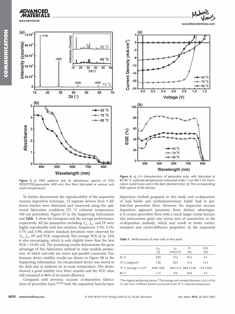
Figure 4 shows the J – V characteristics of 150 nm PbCl 2 (430 nm perovskite) devices. The fabrication condition was kept the same as for the above-mentioned cells. The only control variables were the substrate tempera-ture when the CH 3 NH 3 I layer deposition was performed. The highest-performing device was, as expected, fabricated at a 75 °C sub-strate temperature. The cell delivered a short-circuit current density ( J sc ) of 20.9 mA/cm 2 , an open-circuit voltage ( V oc ) of 1.02 V and a high fi ll factor (FF) of 72.2%, leading to a very high PCE of 15.4%. The effi ciency is among one of the highest PCE values reported in vacuum-deposited perovskite solar cells, which is particularly remarkable given the simple layer-by-layer sequential fabrication and the complete omission of costly organic compounds and high-temperature processes. The sample with the substrate temperature of 65 °C exhibits a kink in the J – V curve and a lower J sc of 14.4 mA/cm 2 , which is caused by the incompletely converted PbCl 2 fi lm near the PEDOT:PSS interface. In contrast, the device with the substrate temperature of 85 °C device exhibits kink-free charac-teristics but the lowest J sc of 9.0 mA/cm 2 and PCE of 4.5%. This result is quite sur-prising because the fi lm exhibits similar absorbance as the 75 °C substrate tempera-ture fi lms. The poor crystallization could be the main reason for the low effi ciency. The external quantum effi ciency (EQE) spec-trum of the 75 °C sample exhibits a high value of 80% across the entire 450 to 750 nm wavelength range, indicating full absorp-tion and effi cient carrier extraction in the 430 nm-thick perovskite fi lm. The smaller EQE value of 60–70% observed at ca. 400 nm is due to the combination effect of the higher refl ection of the glass/air interface and the higher absorption of ITO and PEDOT:PSS at this wavelength. The integrated EQE over AM 1.5G solar photon fl ux estimates a J sc of 20.3 mA/cm 2 , which is consistent with
the measured value obtained from solar simulators. Negli-gible hysteresis of the J – V characteristics was observed for the reverse and forward scan directions (see Figure S5, Sup-porting Information). [ 23–27 ] The J sc of cells with and without a mask has been examined, and the difference was always less than 3% (see Figure S6, Supporting Information). The high performance of champion devices can be attributed to the continuous low-contamination vacuum deposition process throughout the device fabrication, the good crystallinity, and the unusual continuous, homogeneous, and pinhole-free per-ovskite thin fi lms.
Adv. Mater. 2014, 26, 6647–6652
www.advmat.dewww.MaterialsViews.com
Figure 2. a–c) Cross-sectional and d–f) top view SEM images of the perovskite thin fi lms fabricated at substrate temperatures of 65 °C (a,d); 75 °C (b,e); and 85 °C (c,f). g) Tilt-angle SEM image of the perovskite thin fi lm fabricated at 75 °C substrate temperature (magnifi ca-tion: 4500×).
6650 wileyonlinelibrary.com © 2014 WILEY-VCH Verlag GmbH & Co. KGaA, Weinheim
CO
MM
UN
ICATI
ON
To further demonstrate the reproducibility of the sequential vacuum deposition technique, 12 separate devices from 3 dif-ferent batches were fabricated and measured using the opti-mized fabrication conditions (75 °C substrate temperature, 430 nm perovskite). Figure S7 in the Supporting Information and Table 1 show the histogram and the average performance, respectively. All the parameters including V oc , J sc , and FF were highly reproducible with low variation. Impressive 3.5%, 2.1%, 5.7% and 5.9% relative standard deviations were observed for V oc , J sc , FF and PCE, respectively. The average PCE of ca. 14% is also encouraging, which is only slightly lower than the best PCE = 15.4% cell. The promising results demonstrate the great advantage of this fabrication method in solar module produc-tion, of which sub-cells are series and parallel connected. Pre-liminary device stability results are shown in Figure S8 in the Supporting Information. An encapsulated device was stored in the dark and in ambient air at room temperature. The device showed a good stability over three months and the PCE value still remained at 86% of its initial effi ciency.
Compared with previous vacuum co-deposition fabrica-tions of perovskite layer, [ 6,8,28 ] both the sequential layer-by-layer
deposition method proposed in this study and co-deposition of lead halide and methylammonium halide lead to pin-hole-free perovskite fi lms. However, the sequential vacuum deposition approach possesses three distinct advantages: i) It creates perovskite fi lms with a much larger crystal domain size (micrometer grain size versus tens of nanometers in the co-deposition method), which may result in better carrier-transport and carrier-diffusion properties; ii) the sequential
Adv. Mater. 2014, 26, 6647–6652
www.advmat.dewww.MaterialsViews.com
10 20 30 40 50 60 70
0
2x10⁴
4x10⁴
6x10⁴
8x10⁴
1x10⁵
10 20 30 40 50 60
65 oC
85 oC
75 oC(440)(330)
(220)
**
*
Inte
nsi
ty (
cou
nts
)
2θ (°
°
)
* (110)
Inte
nsi
ty (
Co
un
ts)
2θ ( )
(a)
400 500 600 700 8000
1
2
3
4
5
Ab
sorb
ance
Wavelength (nm)
65 oC
75 oC
85 oC
(b)
Figure 3. a) XRD patterns and b) absorbance spectra of ITO/PEDOT:PSS/perovskite (430 nm) thin fi lms fabricated at various sub-strate temperatures.
0.0 0.2 0.4 0.6 0.8 1.0 1.2-24
-20
-16
-12
-8
-4
0
4
65 oC
75 oC
85 oC
(a)
Cu
rren
t D
ensi
ty (
mA
/cm
2 )
Voltage (V)
400 500 600 700 8000
20
40
60
80
100(b)
65 oC
75 oC
85 oC
EQ
E (
%)
Wavelength (nm)
Figure 4. a) J – V characteristics of perovskite solar cells fabricated at 65–85 °C substrate temperatures measured under 1 sun AM 1.5G illumi-nation (solid lines) and in the dark (dashed lines). b) The corresponding EQE spectra of the devices.
Table 1. Performance of solar cells in this work.
V OC [V]
J SC [mA/cm 2 ]
FF [%]
PCE [%]
65 °C 0.93 14.4 45.4 6.1
75 °C (highest) a) 1.02 20.9 72.2 15.4
75 °C (average ± s.d.) b) 0.98 ± 0.03 20.8 ± 0.4 68.6 ± 0.04 13.9 ± 0.82
85 °C 1.13 9.0 44.6 4.5
a) The highest performing device; b) The average and standard deviation (s.d.) of the 12 cells from 3 different batches processed at the 75 °C substrate temperature.

6651wileyonlinelibrary.com© 2014 WILEY-VCH Verlag GmbH & Co. KGaA, Weinheim
CO
MM
UN
ICATIO
N
Adv. Mater. 2014, 26, 6647–6652
www.advmat.dewww.MaterialsViews.com
vacuum deposition method can be analogous to a two-step solution process: [ 10,18,29 ] both sequential vacuum evaporation and the two-step solution process decouple the disposition of the reagent salts and offer an enhanced control over the perovskite morphology by individual manipulation of the lead halide and methylammonium halide deposition parameters; iii) the sublimation temperature of CH 3 NH 3 I in high vacuum (75 °C) is much lower than that of lead halides, C 60 , organic carrier transporting layers, and metals (all >250 °C). Sequen-tial layer-by-layer vacuum deposition offers the possibility of dedicated chambers for each layer, which can minimize the contamination issue of CH 3 NH 3 I resublimation when higher-evaporation-temperature materials are evaporated.
In conclusion, we have developed a novel sequential layer-by-layer vacuum sublimation method to fabricate planar-type organometal halide perovskite solar cells. A clear fabrication-condition-morphology-device-performance correlation was observed. The sublimed PbCl 2 converted to perovskite in situ upon CH 3 NH 3 I deposition, resulting in a uniform thin fi lm with unusual large-scale homogeneous crystalline structures at an optimized substrate temperature. By sandwiching these vacuum-deposited perovskite fi lms between the anode and vacuum sublimed electron-transporting layers and the cathode, the simple device architecture delivered a remarkable perfor-mance of V oc = 1.02 V, J sc = 20.89 mA/cm 2 , FF = 72.2% and PCE as high as 15.4%. The cells also exhibited a promising reproducibility with an average PCE of ca. 14% and a relative standard deviation as small as 6%. We envision that the inte-gration of a simplifi ed device structure, simple layer-by-layer fabrication, a low-contamination and highly homogeneous sub-100 °C vacuum process, low-cost raw materials and the compat-ibility of a matured mass-production infrastructure will make this particular method a promising technology that brings per-ovskite solar cells a large step closer to commercial production.
Experimental Section Device and Thin-Film Preparation : The devices were prepared on
cleaned ITO substrates by spin coating a PEDOT:PSS (Clevios AI 4083) thin fi lm. Then, the substrates were loaded into a high vacuum chamber (base pressure < 1 × 10 −6 Torr) to evaporate PbCl 2 , CH 3 NH 3 I, C 60 , Bphen, Ca, Ag thin fi lms layer-by-layer. The substrates were kept at room temperature, and all the layers (PbCl 2 , C 60 , Bphen, Ca, and Ag) were fabricated with constant deposition rates except the CH 3 NH 3 I layer. The substrates were controlled at specifi c temperatures (room temperature, 65 °C, 75 °C and 85 °C), while the CH 3 NH 3 I layers were deposited with a constant source temperature of 85 °C. The devices were confi gured as: glass substrate/ITO (145 nm)/PEDOT:PSS (30 nm)/CH 3 NH 3 PbI 3− x Cl x /C 60 (100 nm)/Bphen (6 nm)/Ca (1 nm)/Ag (120 nm). The devices were encapsulated using a UV-cured sealant (Everwide Chemical Co., Epowide EX) and a cover glass under an anhydrous nitrogen atmosphere after fabrication and subsequently characterized in air.
Characterization : Perovskite thin fi lms for SEM, AFM, XRD and absorption measurements were prepared using the same fabrication conditions as for the solar cells with layer structures confi gured as: glass substrate/ITO (145 nm)/PEDOT:PSS (30 nm)/CH 3 NH 3 PbI 3− x Cl x . The SEM images were obtained using a Japan Electron Optics Laboratory Co., Ltd. (JEOL) JSM-7000F scanning electron microscope. The AFM images were acquired using a Bruker Dimension Icon atomic force microscope. The X-ray diffraction was performed using a Rigaku TTRAX III instrument with Cu K α radiation. The absorption spectra were
acquired using a SHIMADZU UV-2600 UV–vis spectrophotometer. The current density versus voltage ( J – V ) characteristics of the devices were measured using a Keithley SourceMeter 2636A in the dark and under AM 1.5G simulated solar illumination with an intensity of 100 mW/cm 2 (1 sun, calibrated by a NREL-traceable KG5 fi ltered silicon reference cell). The ITO anode and the metal cathode were arranged in a cross-bar geometry and the device area was determined by the overlap of the ITO and the metal electrodes. Accurate device areas (ca. 0.05 cm 2 ) were measured device-by-device using a calibrated optical microscope. The EQE spectra were acquired by illuminating a chopped monochromatic light with a continuous-wave bias white light (from halogen lamp) on the solar cells. The monochromatic light intensities were measured with a NIST-traceable power meter (Ophir). The photocurrent signals were then extracted using the lock-in technique using a current preamplifi er (Stanford Research System) followed by a lock-in amplifi er (AMETEK).
Supporting Information Supporting Information is available from the Wiley Online Library or from the author.
Acknowledgements The authors would like to acknowledge the fi nancial support from the Ministry of Science and Technology of Taiwan (102–2221-E-007–125-MY3, 101–2112-M-007–017-MY3, 102–2633-M-007–002, 103-3113-E-007-004) and the Low Carbon Energy Research Center, National Tsing Hua University.
Received: June 3, 2014 Revised: July 18, 2014
Published online: September 1, 2014
[1] A. Kojima , K. Teshima , Y. Shirai , T. Miyasaka , J. Am. Chem. Soc. 2009 , 131 , 6050 .
[2] J. H. Noh , S. H. Im , J. H. Heo , T. N. Mandal , S. I. Seok , Nano Lett. 2013 , 13 , 1764 .
[3] P. Qin , S. Tanaka , S. Ito , N. Tetreault , K. Manabe , H. Nishino , M. K. Nazeeruddin , M. Grätzel , Nat. Commun. 2014 , 5 , 3834 .
[4] A. Yella , L. P. Heiniger , P. Gao , M. K. Nazeeruddin , M. Grätzel , Nano Lett. 2014 , 14 , 2591 .
[5] S. Ryu , J. H. Noh , N. J. Jeon , Y. C. Kim , W. S. Yang , J. W. Seo , S. I. Seok , Energy Environ. Sci. 2014 , 7 , 2614 .
[6] O. Malinkiewicz , A. Yella , Y. H. Lee , G. M. Esoallargas , M. Grätzal , M. K. Nazeeruddin , H. J. Bolink , Nat. Photonics 2014 , 8 , 128 .
[7] N. Pellet , P. Gao , G. Gregori , T. Y. Yang , M. K. Nazeeruddin , J. Maier , M. Grätzel , Angew. Chem. Int. Ed. Engl. 2014 , 53 , 3151 .
[8] M. Liu , M. B. Johnston , H. J. Snaith , Nature 2013 , 501 , 395 . [9] Q. Chen , H. Zhou , Z. Hong , S. Luo , H. S. Duan , H. H. Wang , Y. Liu ,
G. Li , Y. Yang , J. Am. Chem. Soc. 2014 , 136 , 622 . [10] J. Burschka , N. Pellet , S. J. Moon , R. Humphry-Baker , P. Gao ,
M. K. Nazeeruddin , M. Grätzel , Nature 2013 , 499 , 316 . [11] J. M. Ball , M. M. Lee , A. Hey , H. J. Snaith , Energy Environ. Sci. 2013 ,
6 , 1739 . [12] Y. H. Hu , Adv. Mater. 2014 , 26 , 2102 . [13] G. E. Eperon , V. M. Burlakov , P. Docampo , A. Goriely , H. J. Snaith ,
Adv. Funct. Mater. 2014 , 24 , 151 . [14] B. Conings , L. Baeten , C. De Dobbelaere , J. D'Haen , J. Manca ,
H. G. Boyen , Adv. Mater. 2014 , 26 , 2041 . [15] P. W. Liang , C. Y. Liao , C. C. Chueh , F. Zuo , S. T. Williams , X. K. Xin ,
J. Lin , A. K. Jen , Adv. Mater. 2014 , 26 , 3748 . [16] J. Y. Jeng , Y. F. Chiang , M. H. Lee , S. R. Peng , T. F. Guo , P. Chen ,
T. C. Wen , Adv. Mater. 2013 , 25 , 3727 .

6652 wileyonlinelibrary.com © 2014 WILEY-VCH Verlag GmbH & Co. KGaA, Weinheim
CO
MM
UN
ICATI
ON [17] J. Y. Jeng , K. C. Chen , T. Y. Chiang , P. Y. Lin , T. D. Tsai , Y. C. Chang ,
T. F. Guo , P. Chen , T. C. Wen , Y. J. Hsu , Adv. Mater. 2014 , 26 , 4107 .
[18] D. Bi , S.-J. Moon , L. Häggman , G. Boschloo , L. Yang , E. M. J. Johansson , M. K. Nazeeruddin , M. Grätzel , A. Hagfeldt , RSC Adv. 2013 , 3 , 18762 .
[19] H. S. Kim , C. R. Lee , J. H. Im , K. B. Lee , T. Moehl , A. Marchioro , S. J. Moon , R. Humphry-Baker , J. H. Yum , J. E. Moser , M. Grätzel , N. G. Park , Sci. Rep. 2012 , 2 , 591 .
[20] Y. Ma , L. Zheng , Y. H. Chung , S. Chu , L. Xiao , Z. Chen , S. Wang , B. Qu , Q. Gong , Z. Wu , X. Hou , Chem. Commun. 2014 , DOI: 10.1039/c4cc01962h .
[21] H.-W. Lin , H.-W. Kang , Z.-Y. Huang , C.-W. Chen , Y.-H. Chen , L.-Y. Lin , F. Lin , K.-T. Wong , Org. Electron. 2012 , 13 , 1925 .
[22] K. Liang , D. B. Mitzi , M. T. Prikas , Chem. Mater. 1998 , 10 , 403 .
[23] H. J. Snaith , A. Abate , J. M. Ball , G. E. Eperon , T. Leijtens , N. K. Noel , S. D. Stranks , J. T. -W. Wang , K. Wojciechowski , W. Zhang , J. Phys. Chem. Lett. 2014 , 5 , 1511 .
[24] Z. Xiao , C. Bi , Y. Shao , Q. Dong , Q. Wang , Y. Yuan , C. Wang , Y. Gao , J. Huang , Energy Environ. Sci. 2014 , 7 , 2619 .
[25] J.-W. Lee , D.-J. Seol , A.-N. Cho , N.-G. Park , Adv. Mater. 2014 , DOI: 10.1002/adma.201401137 .
[26] Q. Wang , Y. Shao , Q. Dong , Z. Xiao , Y. Yuan , J. Huang , Energy Environ. Sci. 2014 , 7 , 2359 .
[27] O. Malinkiewicz , C. Roldán-Carmona , A. Soriano , E. Bandiello , L. Camacho , M. K. Nazeeruddin , H. J. Bolink , Adv. Energy Mater. 2014 , DOI: 10.1002/aenm.201400345 .
[28] C. Roldan-Carmona , O. Malinkiewicz , A. Soriano , G. Minguez Espallargas , A. Garcia , P. Reinecke , T. Kroyer , M. I. Dar , M. K. Nazeeruddin , H. J. Bolink , Energy Environ. Sci. 2014 , 7 , 994 .
[29] D. Liu , T. L. Kelly , Nat. Photonics 2014 , 8 , 133 .
Adv. Mater. 2014, 26, 6647–6652
www.advmat.dewww.MaterialsViews.com