effect of argon-oxygen flow rate ratio in magnetron
TRANSCRIPT

Int. J. Electrochem. Sci., 11 (2016) 6886 – 6901, doi: 10.20964/2016.08.45
International Journal of
ELECTROCHEMICAL SCIENCE
www.electrochemsci.org
Effect of Argon-Oxygen Flow Rate Ratio in Magnetron
Sputtering on Morphology and Hygroscopic Property of SnO2
Thin Film
M. Faris Shahin Shahidan and R. Awang*
School of Applied Physics, Faculty of Science and Technology, Universiti Kebangsaan Malaysia,
43600 UKM Bangi, Selangor, Malaysia. *E-mail: [email protected]
Received: 31 March 2016 / Accepted: 11 May 2016 / Published: 7 July 2016
Thin films of tin dioxide (SnO2) were deposited by DC magnetron sputtering on quartz substrate at
room temperature in different argon-oxygen gas flow rate ratio i.e. Ar:O2 = 100:20 sccm, 90:30 sccm,
80:40 sccm, 70:50 sccm and 60:60 sccm. X-ray diffraction (XRD) patterns show that as-deposited
SnO2 thin films are amorphous. Post-annealing process in air at 500˚C for 1 h resulted in
semicrystalline SnO2 that has tetragonal structure with spatial group of P42/mnm (136). Transmission
electron microscope (TEM) analysis confirmed that the semicrystalline nature of the films after
annealing was due to crystal growth. The surface morphology studied by field emission scanning
electron microscope (FESEM) shows that the increase of argon flow rate lead to increment of the
thickness and the crack size on the films surface. From the humidity response test, SnO2 thin film that
was deposited at maximum argon flow and minimum oxygen flow rate i.e Ar:O2 = 100:20 showed
negative sensitivity gradient. This shows that it has an opposing behaviour from n-type semiconductor
due to its non-stoichiometric state caused by high oxygen vacancies. While SnO2 thin film that was
deposited at minimum argon flow and maximum oxygen flow rate i.e. Ar:O2 = 60:60 showed the
highest sensitivity (positive gradient) with slight fluctuation of repeatability. It was determined that at
argon-oxygen flow rate ratio of Ar:O2 = 70:50 yielded a SnO2 thin film with high sensitivity (positive
gradient) and good repeatability towards relative humidity showing it is environmentally stable.
Keywords: Cracks, FESEM, Humidity, TEM, Thickness.
1. INTRODUCTION
Tin dioxide (SnO2) is a wide band gap n-type semiconductor (Eg= 3.6-4.0 eV) with many
interesting properties. Optically, an undoped SnO2 thin film is highly transparent with an optical

Int. J. Electrochem. Sci., Vol. 11, 2016
6887
transmittance of >80% in visible range. The film also has low resistivity ranging from ρ = 10-3
- 100
Ωcm. SnO2 thin films are low cost, chemically stable, mechanically hard and can resist high
temperature [5]. Therefore, SnO2 thin films are versatile for various applications such as solar cells,
optoelectronic devices, photocatalyst and sensors.
The use of SnO2 as material in chemical sensor especially gas sensors has wide applications in
industries. Since SnO2 was introduced and patented as gas sensor in 1962 [8], it has undergone various
research and development to improve its quality as gas sensor. In the form of thin films, it has growing
popularity among researchers due to its flexibility and unique properties compared to bulk form.
Besides, the hygroscopic property of SnO2 has also been reported. An n-type semiconductor like SnO2
would increase in conductivity when interacting with water molecules [6]. Moreover SnO2 exhibits
electronic conductivity at low temperature, thus SnO2 based humidity sensor is expected [6]. However,
the hygroscopic properties of SnO2 in the form of thin films are seldom reported and discussed.
There are various deposition techniques used to prepare SnO2 films such as spray pyrolysis,
spin coating, thermal evaporation, chemical vapour deposition and sputtering. Among of the
techniques, magnetron sputtering is known for its simplicity, provides controllable critical process
parameters [9], high deposition rate, competitive costs, good reproducibility [10] and has wide range of
materials that can be deposited [4]. In magnetron sputtering, the process parameters are very important
to produce thin films with desired qualities. Parameters such as supplied power, type of reactive gas,
partial gas pressure, gas flow rate, substrate temperature and deposition temperature can be tuned to
deposit thin films of different properties.
In this paper, magnetron sputtered SnO2 thin films were deposited at different flow rate ratio of
reactive and sputerring gas i.e. oxygen and argon. Its effect on the films morphology was examined.
Then, the response of the produced SnO2 thin films towards relative humidity was also tested to
determine optimum parameter in producing SnO2 thin films with good hygroscopic properties.
2. MATERIALS AND METHOD
SnO2 thin films were deposited on an unheated quartz substrate from a 3.2 cm diameter tin (Sn)
target with 99.999% purity using DC magnetron sputtering technique.
Table 1. Parameters used in magnetron sputtering during SnO2 films deposition
Parameters Details
Target Tin, Sn (99.999% purity)
DC power 30 W
Deposition duration 40 min
Flow rate ratio of Ar:O2 (sccm) 60:60, 70:50, 80:40, 90:30, 100:20
Deposition temperature Room temperature (~27˚C)

Int. J. Electrochem. Sci., Vol. 11, 2016
6888
The magnetron sputtering system used was Kurt J. Lesker’s PVD 75 model. DC power of 30 W
was supplied and the films were deposited at different argon-oxygen gas flow rate ratio, Ar:O2 of
100:20 sccm, 90:30 sccm, 80:40 sccm, 70:50 sccm and 60:60 sccm, for 40 min at room temperature.
The SnO2 films were then annealed at 500˚C in air for 1 h. Table 1 shows the summary of the
deposition parameters used.
Both as-deposited and annealed SnO2 thin films were characterized for their crystal structure
using Bruker D8 Advance X-ray diffractometer which is equipped with CuKα radiation source. The
surface morphology and thickness of the films deposited at Ar:O2 = 100:20, 80:40 and 60:60 were
analysed using field emission scanning electron microscopy (FESEM) (Supra 55 VP). The details of
the morphology for the samples were analysed using transmission electron microscope (TEM) using
JEOL USA’s JEM-2100F.
Figure 1. (a) Block diagram of humidity sensing test system. (b) Component of the voltage divider
circuit in the test chamber.
(a)
(b)
Int. J. Electrochem. Sci., Vol. 11, 2016
6889
Before the humidity response tests were carried out, interdigitated silver (Ag) electrodes were
deposited on top of the SnO2 films which method has been described elsewhere [2]. A home-built
humidity sensing test system (Fig. 1(a)) was used to test the films for their sensitivity and repeatability
in changing humid environment at room temperature. The test chamber is consist of commercially
available humidity sensor to measure %RH and a voltage divider circuit (Fig. 1(b)) to measure voltage
change (V) of the thin film in dry and humid condition. R0 is a resistant with known resistance act as a
control while Vin is the voltage supplied by the DC source. The resistance of thin films (RRH) was then
calculated from Eq. 1 shown below.
(1)
Both measurements are then acquired by the data acquisition system. To establish both dry and
humid conditions, the system has three valves labeled 1, 2 and 3. N2 gas which act as dry air was made
to flow through valve 1 in direction of (A) directly to the test chamber, thus create dry condition.
Valve 2 and valve 3 on the other hand, allow N2 gas to flow through water-filled conical flask, creating
humid air to flow in (B) direction towards the test chamber. Both path (A) and (B) were alternately
opened to test for thin film repeatability. The sensitivity, S was determined using the Eq. 2 below:
(2)
where RRH is resistance of thin film at any %RH while RRHmax is maximum resistance achieved
by the thin film at particular %RH.
3. RESULTS AND DISCUSSION
A

Int. J. Electrochem. Sci., Vol. 11, 2016
6890
B
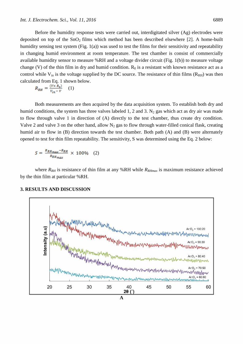
Figure 2. XRD diffractograms for (a) as-deposited and (b) post-annealed SnO2 thin films deposited at
different Ar:O2 flow rate ratio. The diffraction peaks appeared due to annealing process.
Fig. 2 shows the XRD diffractograms of the as-deposited and annealed SnO2 thin films. The
absence of diffraction peak in Fig. 2(a) indicates that the as-deposited thin film is amorphous in nature.
In Fig. 2(b), the appearance of major peaks at 2θ = 26.5˚, 33.8˚, 37.9˚ and 51.7˚ which correspond to
(110), (101), (200) and (211) plane [11] shows crystallinity of the thin films improved after annealing
process.

Int. J. Electrochem. Sci., Vol. 11, 2016
6891
Figure 3. Micrograph of topography of (a) as-deposited and (b) post-annealed SnO2 thin film
deposited at Ar:O2 = 100:20
However, the slight displacement at 2θ = 20˚ - 25˚ suggested that the post-annealed SnO2 thin
films are composed of semicrystalline SnO2 with tetragonal structure and spatial group of P42/mnm
(136). The increase in peak intensity with increasing argon flow rate indicated that the films have
increasing number of SnO2 particles deposited on the substrate. The formation of (110) plane is very
important for sensor application because it helps to increase the oxygen vacancies at low temperature
[12]. This is because the formation of oxygen vacancies on the surface of SnO2 thin films can enhance
the process of adsorption and desorption [6]. Thus the increase in peak intensity corresponding to
(110) plane shows increment of oxygen vacancies on the films. The d-spacing for the (110) plane
calculated from the XRD diagram is 0.351 nm.

Int. J. Electrochem. Sci., Vol. 11, 2016
6892
Figure 4. FESEM micrograph showing topography of SnO2 thin films deposited at Ar:O2 (a) 100:20,
(b) 80:40 and (c) 60:60 sccm.
The surface morphology of the SnO2 thin films was obtained from the FESEM, as shown in
Fig. 3 and Fig. 4. From the Fig. 3, the inhomogeneity of the surface of the as-deposited film was due to
agglomeration of SnO2 particles during film deposition. However, the homogeneity of the film was
improved and no agglomeration was observed after the annealing process. There was also slight
increase in the crack size due to the heat treatment. Table 2 shows the deposition rate and thickness of
the films deposited at Ar:O2 = 100:20, 80:40 and 60:60 sccm that were obtained from FESEM. The
thickness of the films increased with argon flow rate. An increase in argon content during deposition
can increase the thickness of the films [13]. This is because when more argon ions were formed during
deposition, the sputtering rate and deposition rate of SnO2 were also increased and thus caused
thickness of the films to increase.

Int. J. Electrochem. Sci., Vol. 11, 2016
6893
Table 2. Thickness and deposition rate for SnO2 thin film deposited at different Ar:O2
Ar (sccm) O2 (sccm) Thickness
(nm)
Deposition rate
(nm/min)
100 20 118.4 2.96
80 40 29.03 0.72
60 60 21.21 0.53
Int. J. Electrochem. Sci., Vol. 11, 2016
6894
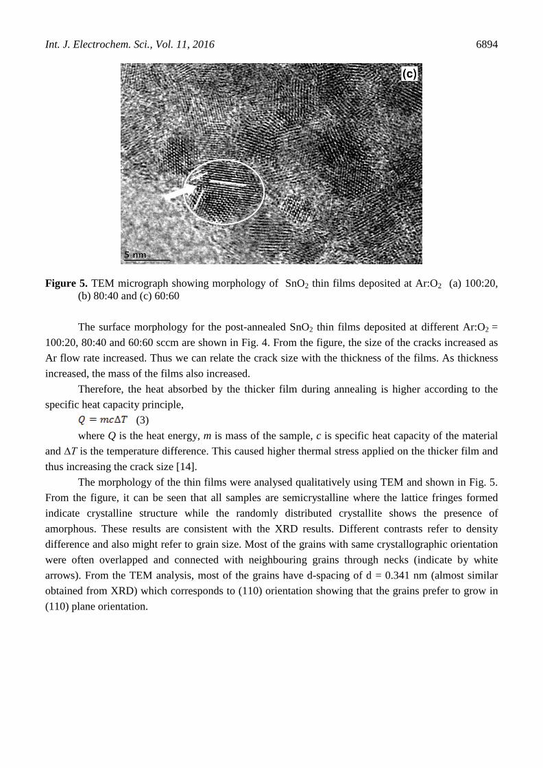
Figure 5. TEM micrograph showing morphology of SnO2 thin films deposited at Ar:O2 (a) 100:20,
(b) 80:40 and (c) 60:60
The surface morphology for the post-annealed SnO2 thin films deposited at different Ar:O2 =
100:20, 80:40 and 60:60 sccm are shown in Fig. 4. From the figure, the size of the cracks increased as
Ar flow rate increased. Thus we can relate the crack size with the thickness of the films. As thickness
increased, the mass of the films also increased.
Therefore, the heat absorbed by the thicker film during annealing is higher according to the
specific heat capacity principle,
(3)
where Q is the heat energy, m is mass of the sample, c is specific heat capacity of the material
and ∆T is the temperature difference. This caused higher thermal stress applied on the thicker film and
thus increasing the crack size [14].
The morphology of the thin films were analysed qualitatively using TEM and shown in Fig. 5.
From the figure, it can be seen that all samples are semicrystalline where the lattice fringes formed
indicate crystalline structure while the randomly distributed crystallite shows the presence of
amorphous. These results are consistent with the XRD results. Different contrasts refer to density
difference and also might refer to grain size. Most of the grains with same crystallographic orientation
were often overlapped and connected with neighbouring grains through necks (indicate by white
arrows). From the TEM analysis, most of the grains have d-spacing of d = 0.341 nm (almost similar
obtained from XRD) which corresponds to (110) orientation showing that the grains prefer to grow in
(110) plane orientation.

Int. J. Electrochem. Sci., Vol. 11, 2016
6895
Figure 6. TEM micrograph showing the formation of nanocluster during crystal growth process in
post-annealed SnO2 thin films
The presence of nanoclusters made by overlapped and connected neighbouring grains
suggested that the grain growth process occurred during annealing. According to Chen et al. [6], there
are four phases of grain growth process in SnO2 thin films which starts with nucleation, followed by
grain rotation, coalescence and finally the growth of nanoclusters. These phases can be shown in TEM
micrograph in Fig. 6.
Int. J. Electrochem. Sci., Vol. 11, 2016
6896
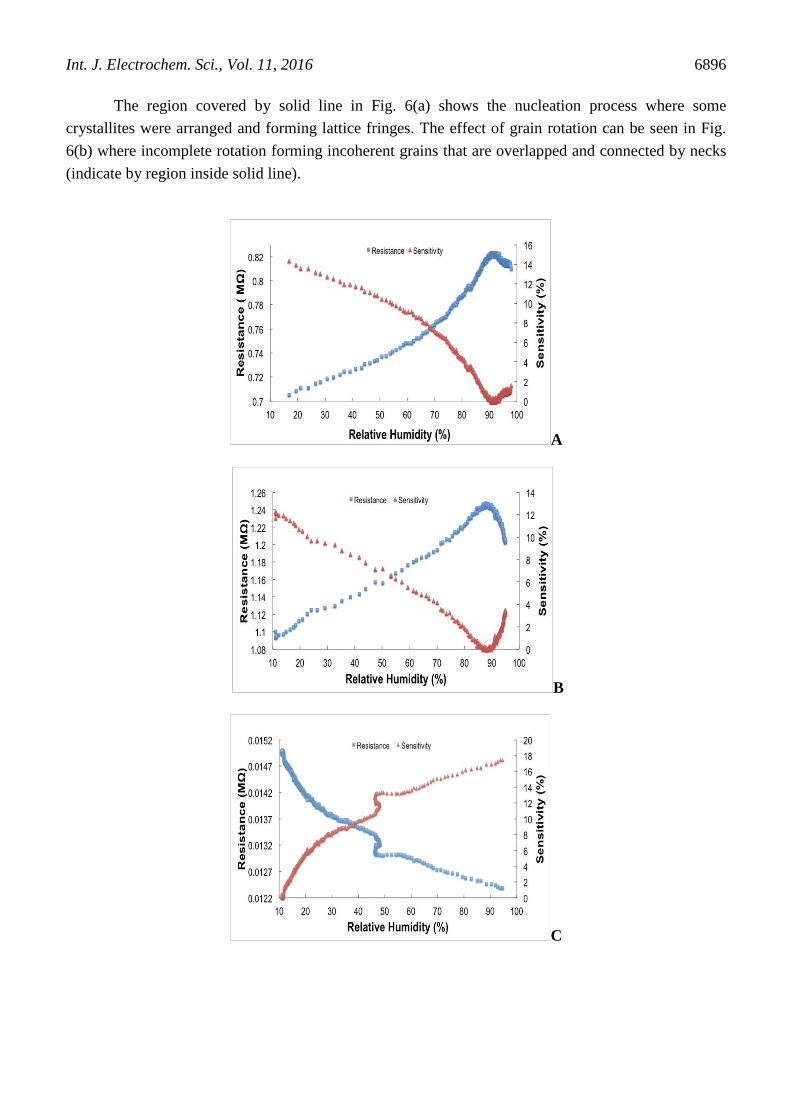
The region covered by solid line in Fig. 6(a) shows the nucleation process where some
crystallites were arranged and forming lattice fringes. The effect of grain rotation can be seen in Fig.
6(b) where incomplete rotation forming incoherent grains that are overlapped and connected by necks
(indicate by region inside solid line).
A
B
C
Int. J. Electrochem. Sci., Vol. 11, 2016
6897
D
E
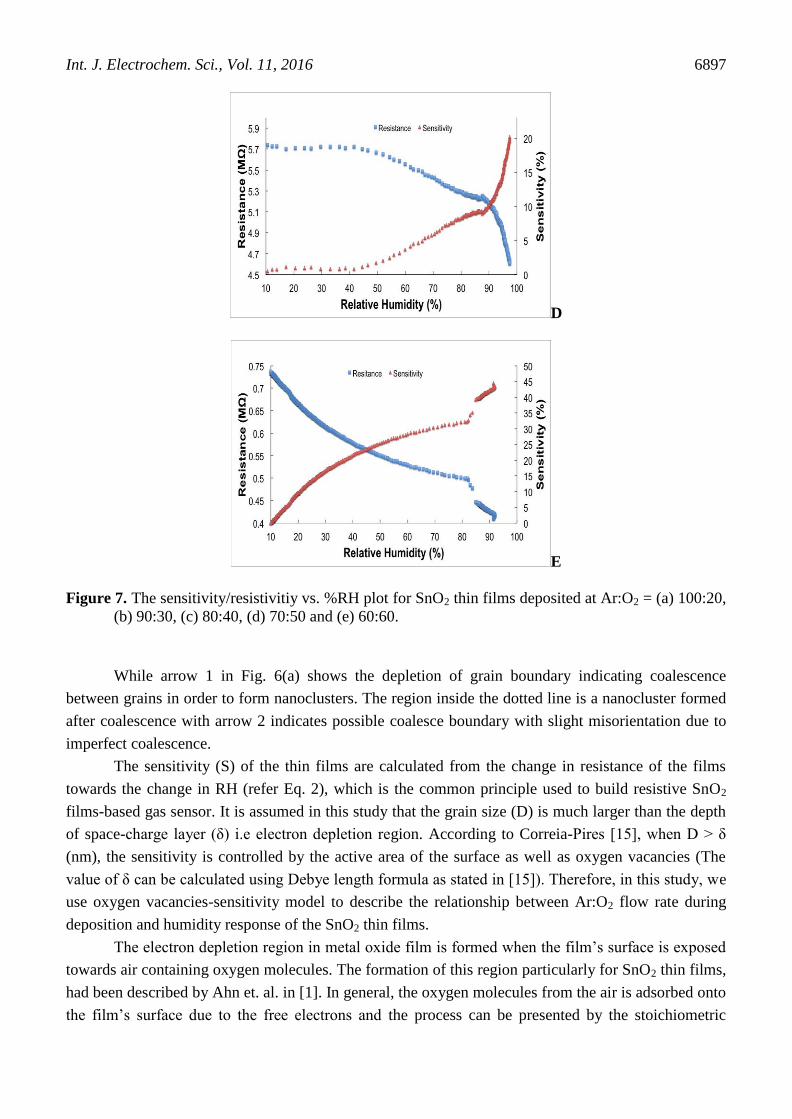
Figure 7. The sensitivity/resistivitiy vs. %RH plot for SnO2 thin films deposited at Ar:O2 = (a) 100:20,
(b) 90:30, (c) 80:40, (d) 70:50 and (e) 60:60.
While arrow 1 in Fig. 6(a) shows the depletion of grain boundary indicating coalescence
between grains in order to form nanoclusters. The region inside the dotted line is a nanocluster formed
after coalescence with arrow 2 indicates possible coalesce boundary with slight misorientation due to
imperfect coalescence.
The sensitivity (S) of the thin films are calculated from the change in resistance of the films
towards the change in RH (refer Eq. 2), which is the common principle used to build resistive SnO2
films-based gas sensor. It is assumed in this study that the grain size (D) is much larger than the depth
of space-charge layer (δ) i.e electron depletion region. According to Correia-Pires [15], when D > δ
(nm), the sensitivity is controlled by the active area of the surface as well as oxygen vacancies (The
value of δ can be calculated using Debye length formula as stated in [15]). Therefore, in this study, we
use oxygen vacancies-sensitivity model to describe the relationship between Ar:O2 flow rate during
deposition and humidity response of the SnO2 thin films.
The electron depletion region in metal oxide film is formed when the film’s surface is exposed
towards air containing oxygen molecules. The formation of this region particularly for SnO2 thin films,
had been described by Ahn et. al. in [1]. In general, the oxygen molecules from the air is adsorbed onto
the film’s surface due to the free electrons and the process can be presented by the stoichiometric
Int. J. Electrochem. Sci., Vol. 11, 2016
6898
formula below. Higher oxygen vacancies lead to a higher density of free electron thus increase the
thickness of the adsorbed oxygen ion layer formed at the film’s surface. In this study, oxygen
vacancies of the films are highly dependent on the Ar:O2 flow rate.
When the surface is exposed to humid air with a significant amount of water molecules (H2O),
the oxygen ions were replaced by the H2O which is adsorbed on the oxide surface in the hydroxyl
forms [6]. This is caused by the competitive adsorption between oxygen ions and H2O molecules and
thus desorption of O- by releasing electrons (which process is the reverse of above stoichiometric
formula). This will neutralize the electron depletion region. According to Chen & Lu [6], the H2O
molecules behaves as electron donors to the film’s surface and deduced that for the n-type metal oxide
thin film like SnO2, the competitive adsorption will increase the conductivity of the surface (lower
resistivity) and thus increases sensitivity.
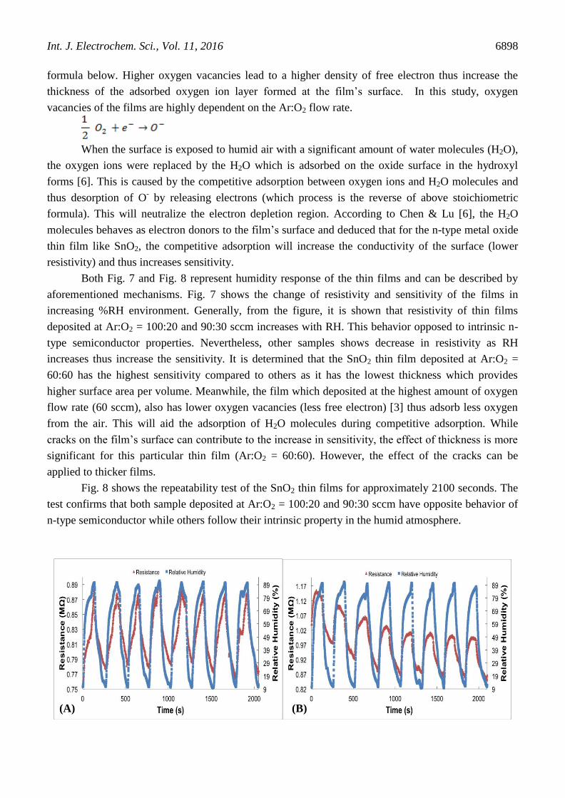
Both Fig. 7 and Fig. 8 represent humidity response of the thin films and can be described by
aforementioned mechanisms. Fig. 7 shows the change of resistivity and sensitivity of the films in
increasing %RH environment. Generally, from the figure, it is shown that resistivity of thin films
deposited at Ar:O2 = 100:20 and 90:30 sccm increases with RH. This behavior opposed to intrinsic n-
type semiconductor properties. Nevertheless, other samples shows decrease in resistivity as RH
increases thus increase the sensitivity. It is determined that the SnO2 thin film deposited at Ar:O2 =
60:60 has the highest sensitivity compared to others as it has the lowest thickness which provides
higher surface area per volume. Meanwhile, the film which deposited at the highest amount of oxygen
flow rate (60 sccm), also has lower oxygen vacancies (less free electron) [3] thus adsorb less oxygen
from the air. This will aid the adsorption of H2O molecules during competitive adsorption. While
cracks on the film’s surface can contribute to the increase in sensitivity, the effect of thickness is more
significant for this particular thin film (Ar:O2 = 60:60). However, the effect of the cracks can be
applied to thicker films.
Fig. 8 shows the repeatability test of the SnO2 thin films for approximately 2100 seconds. The
test confirms that both sample deposited at Ar:O2 = 100:20 and 90:30 sccm have opposite behavior of
n-type semiconductor while others follow their intrinsic property in the humid atmosphere.
(B) (A)
Int. J. Electrochem. Sci., Vol. 11, 2016
6899
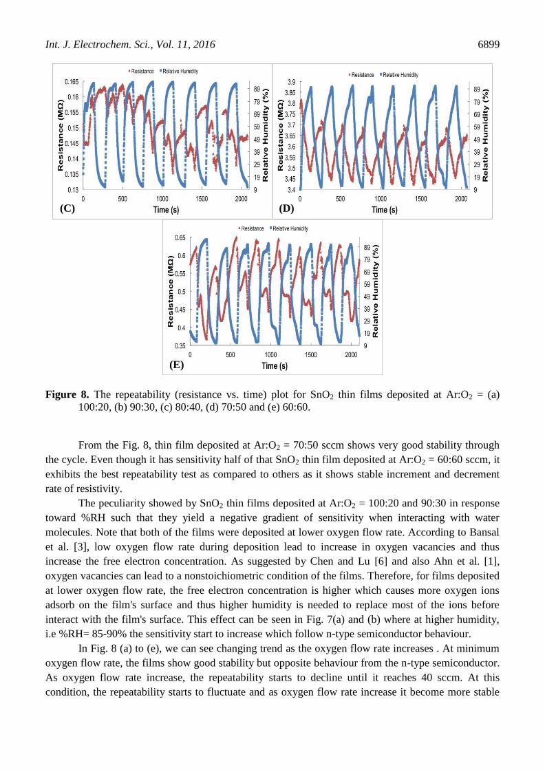
Figure 8. The repeatability (resistance vs. time) plot for SnO2 thin films deposited at Ar:O2 = (a)
100:20, (b) 90:30, (c) 80:40, (d) 70:50 and (e) 60:60.
From the Fig. 8, thin film deposited at Ar:O2 = 70:50 sccm shows very good stability through
the cycle. Even though it has sensitivity half of that SnO2 thin film deposited at Ar:O2 = 60:60 sccm, it
exhibits the best repeatability test as compared to others as it shows stable increment and decrement
rate of resistivity.
The peculiarity showed by SnO2 thin films deposited at Ar:O2 = 100:20 and 90:30 in response
toward %RH such that they yield a negative gradient of sensitivity when interacting with water
molecules. Note that both of the films were deposited at lower oxygen flow rate. According to Bansal
et al. [3], low oxygen flow rate during deposition lead to increase in oxygen vacancies and thus
increase the free electron concentration. As suggested by Chen and Lu [6] and also Ahn et al. [1],
oxygen vacancies can lead to a nonstoichiometric condition of the films. Therefore, for films deposited
at lower oxygen flow rate, the free electron concentration is higher which causes more oxygen ions
adsorb on the film's surface and thus higher humidity is needed to replace most of the ions before
interact with the film's surface. This effect can be seen in Fig. 7(a) and (b) where at higher humidity,
i.e %RH= 85-90% the sensitivity start to increase which follow n-type semiconductor behaviour.
In Fig. 8 (a) to (e), we can see changing trend as the oxygen flow rate increases . At minimum
oxygen flow rate, the films show good stability but opposite behaviour from the n-type semiconductor.
As oxygen flow rate increase, the repeatability starts to decline until it reaches 40 sccm. At this
condition, the repeatability starts to fluctuate and as oxygen flow rate increase it become more stable
(E)
(D) (C)
Int. J. Electrochem. Sci., Vol. 11, 2016
6900
until eventually follow n-type semiconductor behaviour. This response shows that oxygen flow rate of
40 sccm as the turning point of the films’ behavior from opposing n-type semiconductor towards its
intrinsic property. Thus, we can say that both SnO2 thin films deposited at Ar:O2 of 100:20 and 90:30
are not environmentally stable due to nonstoichiometric condition and tend to oppose its intrinsic
behavior.
4. CONCLUSION
From this study, it can be concluded that the as-deposited SnO2 thin films are amorphous.
Annealing process aids the crystal growth and thus crystallizes the SnO2 thin films. Therefore,
semicrystalline SnO2 thin films with tetragonal structure and spatial group of P42/mnm (136) were
successfully obtained. The simultaneous increase of argon flow rate and decrease of oxygen flow rate
influenced the morphology of the films and their response towards humidity. The SnO2 thin film
deposited at maximum argon flow rate but minimum oxygen flow rate i.e Ar:O2 = 100:20, has opposite
behaviour from n-type semiconductor due to high oxygen vacancies which lead to its non-
stoichiometric state. Apparently, SnO2 thin film deposited at minimum argon flow rate but maximum
oxygen flow rate i.e. Ar:O2 = 60:60, has highest sensitivity with positive gradient which dominantly
due to its low thickness. It also has good repeatability and environmentally stable. Finally, in
intermediate deposition condition i.e., Ar:O2 = 70:50, SnO2 thin film with high sensitivity towards
humidity, better repeatability and environmentally stable, was yielded. Therefore, argon-oxygen flow
rate ratio, Ar:O2 of 70:50 is the best parameter to deposit a SnO2 thin film with good hygroscopic
property. The results also show that SnO2 thin film can operate at room temperature which makes it
suitable for humidity sensor. The sensitivity of the magnetron sputtered SnO2 thin films could be
enhanced by increasing the chamber pressure during the deposition process while maintaining the
same Ar:O2 ratio at 70:50 sccm. This is because at higher pressure, thin films produced will have lower
oxygen vacancies and thus could increase its sensitivity [15]. As oxygen vacancy is low, the charge
carrier density i.e free electron is also decreased thus attracts less oxygen from air. This established a
lower competitive adsorption between water molecules and the pre-adsorbed oxygen molecules from
air thus subsequently aid the rate of physisorption of water molecules.
While sensitivity of single crystal SnO2 thin film can be enhanced through deposition
condition, doping is another effective method that could be approached to achieve higher sensitivity.
Single crystal thin films are usually lack of exposing surface area which lead to lower sensitivity as
compared to doped thin films [16]. Previous research done [17] shows that the sol-gel prepared Zn-
doped SnO2 thin film comprises of cubic structured crystallites. Higher amount of Zn dopant leads to
more pronounced cubic shape yet smaller in size. This increases the surface area per volume of the thin
film which allows higher adsorption of water molecules thus increases the sensitivity.
ACKNOWLEDGEMENT
The authors gratefully acknowledge the support in the form of a Fundamental Research Grant
Scheme FRGS/2/2013/SG02/UKM/02/1 by Ministry of Higher Education, Malaysia.

Int. J. Electrochem. Sci., Vol. 11, 2016
6901
References
1. H. Ahn, J.H. Noh, ,S.-B. Kim, R.A.Overfelt, Y.S. Yoon, D.-J. Kim, Materials Chemistry and
Physics, 124 (2010) 563-568.
2. N.F.H. Aziz, R. Ritikos, S.A.A Kamal, N.S. Mohamed Hussain, R. Awang, AIP Conference
Proceedings, 1571 (2013) 125-131.
3. S. Bansal, D.K. Pandya, S.C. Kashyap, D. Haranath, Journal of Alloys and Compounds, 583
(2014) 186-190.
4. G. Bräuer, B. Szyszka, M. Vergöhl, R. Bandorf, Vacuum 84 (2010) 1354-1359.
5. M. A. Camacho-López, J. R. Galeana-Camacho, A. Esparza-García, C. Sánchez-Pérez, C. M.
Julien, Surface and Vacuum, Mexican Society of Science and Technology of Surfaces and
Materials, 26 (2013) 95-99.
6. Z. Chen, C. Lu, Humidity Sensor: A Review of Material and Mechanisms, Sensor Letter, (2005)
274-295.
7. Z.W. Chen, Z. Jiao, M.H. Wu, C.H. Shek, C.M.L. Wu, J.K.L. Lai, Progress in Materials Science,
56 (2011) 901-1029.
8. J. Fraden, Handbook Of Modern Sensors: Physics, Designs and Applications, fourth ed., Springer,
New York, 2010.
9. M.A. Gubbins, V. Casey, S.B. Newcomb, Thin Solid Films, 405 (2002) 270-275.
10. D. Leng, L. Wu, H. Jiang, Y. Zhao, J. Zhang, W. Li, L. Feng, International Journal of
Photoenergy, (2012) 1-6.
11. W. Z. Samad, M. S. Muhamad, A. Shafiee and A. A. Yarmo, Sains Malaysiana, 40(3) (2011) 251–
257.
12. F. R. Sensato, R. Custódio, M. Calatayud, A. Beltrán, J. Andrés, J. R. Sambrano, E. Longo,
Surface Science, 511 (2002) 408- 420.
13. S. Saipriya, M. Sultan, R. Singh, Physica B, 406 (2011) 812-817.
14. Z. Tang, P.C.H. Chan, R.K. Sharma, G. Yan, I-M. Hsing, J.K.O. Sin, Sensors and Actuators B, 79
(2001) 39-47.
15. J. M. Correia-Pires, J. B. Almeida, V. Teixeira, Key Engineering Materials, Vols. 230-232 (2002)
388-391.
16. N. D. Md Sin, Mohamad Fadzil Tahar, M. H. Mamat, M. Rusop, Enhancement of Nanocomposite
for Humidity Sensor Application, Recent Trends in Nanotechnology and Materials Science:
Selected Review Papers from the 2013 International Conference on Manufacturing, Optimization,
Industrial and Material Engineering (MOIME 2013), Springer International Publishing (2014): 15-
30.
17. N.D. Md Sin, Noorlaily Samsudin, S. Ahmad, M.H. Mamat, M. Rusop, Procedia Engineering 56 (
2013 ): 801 – 806.
© 2016 The Authors. Published by ESG (www.electrochemsci.org). This article is an open access
article distributed under the terms and conditions of the Creative Commons Attribution license
(http://creativecommons.org/licenses/by/4.0/).