effect of annealing on microstructural development and grain orientation...
TRANSCRIPT

Effect of annealing on microstructural development and
grain orientation in electrodeposited nickel
by
Christos Oikonomou
Diploma work No. 51/2011
at Department of Materials and Manufacturing Technology
CHALMERS UNIVERSITY OF TECHNOLOGY
Gothenburg, Sweden 2011
Diploma work in the master program Applied Physics No. 51/2011
Performed at: Department of Materials and Manufacturing Technology
Chalmers University of Technology
SE-41296 Gothenburg
Examiner and Supervisor: Professor Uta Klement
Department of Materials and Manufacturing Technology
Chalmers University of Technology
SE-41296 Gothenburg

Effect of annealing on microstructural development and grain orientation in electrodeposited nickel
Christos Oikonomou
© Christos Oikonomou 2011
Diploma work No. 51/2011
Department of Materials and Manufacturing Technology
Chalmers University of Technology
SE – 412 96 Gothenburg
Sweden
Telephone +46 (0)31-772 1000
[CHALMERS Reproservice]
Gothenburg, Sweden 2011

ABSTRACT
Pulsed electrodeposition (PED) of nano- and submicrocrystalline materials is a
technologically and economically viable production route for metals, alloys and metal-
matrix composites both in the form of bulk samples and as coatings. Hence,
commercialization of nanomaterials has become attractive and new products for various
applications are being researched and developed. To retain the exceptional macroscopic
properties of nanomaterials also at elevated temperatures, it is essential that the
microstructure of these materials is sufficiently stable upon annealing. Solute additions
have shown to improve the thermal stability of PED materials. But also grain morphology
and texture play an important role for the stability of the material.
Nanocrystalline Ni and Ni alloys electrodeposits have been analyzed in much detail over
the last years. All materials contained additives for more effective grain refinement. In
the present work, submicrocrystalline Ni electrodeposit prepared without additives was
investigated. Results have shown that the microstructure is thermally stable up to at least
325°C, i.e. has a substantially higher thermal stability than Ni with 10 and 20 nm grain
size (stable up to 85°C).
Microstructure and texture development upon annealing of the submicrocrystalline PED-
Ni were analyzed using different microscopical techniques: Electron Backscatter
Diffraction (EBSD), in-situ annealing experiments in TEM and high resolution imaging
in SEM. Texture in as-plated state is different in the submicrocrystalline material as
compared to the nanocrystalline Ni. Instead of a <411> texture, a <110> fibre texture is
found in the growth direction. That texture remains stable at annealing treatment up to
600°C instead evolving to a <111> texture which is frequently observed at
nanocrystalline Ni upon annealing.
The microstructure exhibits a bimodal character with nanometer sized grains surrounding
larger columnar grains of the order of submicrometer. The latter are engaged in group
formations of five folded symmetries around common zone axis having a twin boundary
relationship. These colonies of grains exhibit a <110> texture parallel to the growth
direction of the electrodeposit and appear to be stable both in structure and texture upon
annealing.
Keywords: Nickel electrodeposition, texture, microstructure, annealing, EBSD, TEM

CONTENTS
Introduction
o Electrodeposition
o Texture of Electrodeposits
o Microstructure of Electrodeposits
Aim and Scope
Material under investigation
Experimental procedure
o DSC
o Heat treatment
o EBSD
o Sample preparation
Results
o SEM imaging
o Orientation maps
o Grain size and area determination
o Grain boundary and misorientation analysis
o Texture analysis
o Subset / anti-subset analysis
Discussion
Conclusions and future work
References
Acknowledgments
Appendix
1
Introduction
o Electrodeposition
In the field of advanced materials, electrodeposition technique, also known as
electroplating or electrochemical deposition, holds great interest and has received
significant attention over the years. It has been widely used in industrial production
routes for the last century. Electrodeposition offers the possibility to produce nano- and
submicro- crystalline metals and alloys in either bulk or coating form. This sort of
versatility along with the fact that it is an economical viable production route, are its key
features that make it extremely appealing [1, 2]. A great variety of applications from
electroformed products such as CD stampers, coatings for corrosion or wear resistance,
salvage rework of worn components, power supply and motor applications, decorative
applications and more are accomplishable with electrodeposition [2, 3].
Their enhanced properties in comparison to their conventional polycrystalline
counterparts, is one of the reasons that electrodeposited products have such a broad range
of applications [1, 2]. It is possible to create porous-free products with grain size down to
<10 nm [4]. The unique properties of nano- and submicro-crystalline products are a result
of their increased intercrystalline volume fraction. The latter is the outcome of their
extremely small grain size [5, 6]. Thus, it is of great importance that the initial
microstructure can be retained at elevated temperatures. Studies have shown that by
alloying and/or adding solutes it is possible to improve the thermal stability of the
electrodeposits (EDs) through solute segregation, allotropic phase transformation, as well
as triple junctions and Zener pinning [7, 8]. Also a broader grain size distribution is
considered to be responsible for abnormal grain growth at lower temperatures, but that
was not been observed for Ni EDs with broad and narrow distributions and low impurity
content [7, 9].
Electrodeposition involves the creation of the product through an electrolytic process.
The elements that will form the electrodeposit are dissolved in an electrolytic solution
and with the use of current they are being deposited on a substrate (cathode) [4]. Under
the influence of current, redox reactions are taking place which lead to desorption and
absorption of the material. Those redox reactions are taking place in an aqueous acidic
solution which contains ions of the material to be deposited. For different materials of
interest there are different solutions. Furthermore an electrolyte could contain a stress
reliever and grain refining agent, a grain size inhibitor and a buffering agent. The most
common electrolytes used for the plating of Ni are the Watts solution and the Nickel
sulphamate solution. The first contains Nickel sulphate (NiSO4·6H2O), Nickel chloride
(NiCl2·6H2O) and Boric acid (H3BO3) while the later instead of Nickel sulphate contains
Nickel sulphamate (Ni(SO3N2)·4H2O) as main ingredient.

2
The microstructure and texture of the final product, and subsequently its properties, are
affected by many parameters such as the pH and the temperature of the electrolyte, the
current density, the overvoltage and the presence or absence of additives in the
electrolyte. There is no general rule of how these effect the final product, as they
influence each other. Despite the fact that many efforts have been made to decode the
effect of each parameter in the microstructure and texture, direct comparison is not
always feasible due to the fact that most measurements vary in conditions that they were
performed in.
o Texture of EDs
Many theoretical interpretations have been proposed over time, aiming at explaining the
texture formation of EDs. Two of the most important hypothesis, were assuming either
that texture was a result of competitive nucleation or a result of a growth competition.
Both of these theories were countered and sufficiently disproved through experimental
data from J. Amblard et al [10]. Furthermore he proposed a theory in which he is
explaining the texture formation, supporting the idea of electrodeposition being a strongly
inhibited process [10, 11]. In this theory it is suggested that Ni electrodeposition is
hindered due to reasons of strong interactions between the metallic surface and chemical
species that are capable of being absorbed on it. More specific it is assumed that the
effect of these various inhibitors (Ni(OH)2, gaseous H2, Hads) near the cathode result from
hydrogen codeposition. Amblard et al. also ascribed different inhibitors to different
textures. The [100] fibre texture parallel to the growth direction (GD), which is regarded
as the free mode growth of Ni electrodeposits, is associated with the absorbance of
intermediate (NiOH)ads. Three other textures that are present in Ni electrodeposits <110>,
[210] and <211>, are affected by the presence of Hads, gaseous H2, and Ni(OH)2 inside
the cathodic layer respectively. The difference between the crystallographic directions in
the different brackets is that the ones denoted with [hkl] always represent single crystals
while the ones denoted with <hkl> are three-dimensional crystal clusters. The
aforementioned cases account for deposition of Ni in an additive-free electrolyte. In the
case of severe inhibition, when for instance an organic additive consumes more cathodic
hydrogen, <211> texture is replaced by <111>.
The majority of experimental results, conducted in determining the effect of different
parameters on the final microstructure and texture of the EDs, cite the inhibition theory
and are in agreement with its arguments. Amblard et al [10, 11] tried to present the
significance of the pH value and current density for d.c. conditions by holding the
temperature of the electrolyte constant. For high values of pH and low values of current
density a double fiber texture of <110> and <211> // GD was present while for low
current density and low pH a <110> was dominating. For high values of current density
and low pH values [210] is present, while the free mode growth of [100] was dominating
for medium values for both pH and current density (Figure 1). By holding also all the

3
other parameters constant and changing the temperature of the electrolyte, a change in
texture was noticed from [100] at temperatures above 40°C to [210] at temperatures
below 40°C. The presence of additives in the electrolyte had also significant effect on
texture, changing it to <111> at higher values of pH and current density. At lower and
intermediate values of both pH and current density, the texture changed depending on the
additive used (Figure 2).
Figure 1: Stability of the various fibre textures of nickel electrodeposits versus pH of the
Watts bath and nickel current density (based on figure in [11]).
Figure 2: Stability of various fibre textures of nickel electrodeposits versus nickel current
density and concentration of a) butyne-2-diol 1,4 as inhibitor and b) sodium benzene
sulphonate as inhibitor (based on reference [11]).
a)
b)

4
In order to examine the effect of pulse reversed current on the texture of the EDs, C.
Kollia et al [12] started from well known electrolytic conditions that would lead to known
textures in the d.c. regime, which were close to the ones observed by Amblard et al [10,
11]. Taking into account the argument of inhibition of different chemical species on the
cathode, it was expected that the application of pulse reversed current technique would
have a stronger influence on texture due to the larger influence on the composition on the
catholyte. The results confirmed the idea of inhibition of different chemical species and
concluded that this happens by reinforcing the selective inhibition phenomena.
Further studies aiming at investigating the effect of pulse current on the texture of the
EDs were conducted by El-Sherik et al [13]. In this experimental work, the influence of
pulse on-time, off-time and current density was monitored. The texture of the EDs
changed from a random distribution to a strong (200) fibre texture with increasing on-
time and peak current density, while the off-time seemed to have no effect at all.
Furthermore, the effect of the organic additives such as saccharin on texture was
demonstrated, The texture of the EDs changed from an initial fibre (200) texture to a
(100)(200) double fibre texture parallel to the GD [14].
C. Nielsen et al [15] investigated Ni EDs of <110> // GD fibre texture in TEM. Assuming
the inhibition theory of texture growth by the absorption of hydrogen or amorphous
organic species, such species should be tracable in the deposit’s microstructure in these
analyses. However, no incorporated species were found through the EDs microstructure.
Thus an assumption was made that these must be sufficiently stable on certain crystal
faces to modify growth while at the same time sufficiently unstable so as to allow
decomposition and /or release so as not to be codeposited.
In the examination of different parameters that affect the texture evolution of the EDs,
Goods et al [16] conducted an investigation regarding the temperature change. Nickel
EDs were made by use of the LIGA process. Filtration was also performed on the
electrolytic solution using activated Carbon, removing organic and other electrolyte
species such as borate ion that may act as weak deposition inhibitors. Using an unfiltered
electrolyte and low current densities (3 mA/cm2), EDs exhibited a temperature dependent
instability. At low temperatures (≤ 32°C) an <100> uninhibited growth is observed, while
at 50°C EDs exhibit an <110> inhibited growth, similar to their filtered counterparts. At
high current density (15 mA/cm2) the texture is unaffected by the particle filtering.
Another observation concerns the effect of the substrate on the texture evolution of the
EDs. It has been reported that at the first stage of deposition, the deposit follows the
structure and texture of the substrate [10, 11]. Further away from the near substrate
region, texture and microstructure of the deposit is only governed by the electrochemical
parameters. More experimental work conducted by Ebrahimi. et al [17], supported this

5
argument by using substrates of different crystallographic orientation that proved to have
no effect on the final orientation of the EDs. Kozlov et al [18] claimed that fcc EDs up to
0,5 μm from the substrate, have always an initial <111> texture independent of the
electrochemical parameters. In addition, the usage of amorphous Sb and stainless steel as
substrates, lead them to the suggestion that due to the inert nature of the surfaces any
epitaxial influence of the substrate on the texture can be excluded.
o Microstructure of EDs
Some of the key characteristics of the Ni EDs, which are directly related to their
mechanical properties, are the presence of long columnar grain along the growth
direction, usually surrounded by clusters of coarse and fine grains, and a high fraction of
twin boundaries [11, 19, 20, 21, 22, 23, 24, 25]. A surface roughness due to the difference
in grow rates between some crystals is argued to cause a local changes in electrolytic
conditions and thus conditions for nucleation and appearance of those distinct fine grains
[27]. The presence of the long elongated grains is eliminated in strongly inhibited
conditions, such as the presence of high concentrations of additives in the electrolyte
solution, or by alloying [7, 8, 9, 14, 22, 25, 30]. In the case of Cobalt EDs it has also been
reported that a transition from a columnar structure to an assembly of dihedrals occurs by
reducing the value of the pH of the electrolyte under 3 at 50°C [31]. Also the importance
of temperature in the development of microstructure was noted for Nickel EDs [16]. In an
unfiltered electrolyte at low current densities, the microstructure is fine at the low
temperature of 28°C while it becomes coarser at a high temperature of 50°C. At an
intermediate temperature of 40°C, the microstructure contains a mixture of coarse and
fine grains. Rasmussen et al [19] also observed the effect of temperature on the
microstructure and noted that at lower temperatures smaller grain size was achieved.
Generally it is expected that with increasing current density the grain size should
decrease. Increasing the current density and thus increasing the overvoltage, is
anticipated to lead to grain refinement. Some experimental studies on Nickel and Cobalt
EDs [13, 28, 29] have shown exactly that. However, other studies have shown that the
width of those columnar grains increases not only with the increasing thickness of the
sample, but also with increasing current density [19, 25, 26]. In addition, a correlation
between the decrease in the crystalline size and the loss of texture was mentioned,
attributed to the continuous nucleation of new gains which influence the size and the
severity of the texture [26].
In the microstructure of as-plated Ni and Ni alloys, grain colonies exhibiting symmetries
of uneven numbers are met in twin junctions, parallel or inclined to the growth direction
[11, 23, 27]. Those grains exhibiting the same texture in growth direction are formed
during electrodeposition and share a common zone axis. In addition to low-angle grain
boundaries and general high-angle grain boundaries, these colonies are often related
through {111} twin planes, parallel to the GD. Furthermore it is noted that these colonies

6
of grains frequently exhibit a curvature. It is argued that the presence of defects in the
crystal lattice due to co-deposition of hydrogen or other impurities, rotate the columnar
crystals away from the fast growing direction and thus inhibit their further growth [27].
Aim and scope
Retaining the initial microstructure at elevated temperatures is essential for the
application of EDs. The demise of that initial microstructure leads to the degradation of
their tailored-made properties of the material. Hence, studying possible microstructural
changes in EDs is of extreme importance. Any information obtained will contribute to a
better understanding of the evolution of EDs upon annealing, and can be used for further
improvement. In that context, the aim of the present work is the characterization of
microstructure and texture development upon annealing of Ni pulsed electrodeposit. For
that task, well established microscopic techniques such as Scanning Electron Microscopy,
Electron Backscatter Diffraction and Transmission Electron Microscopy were used. The
observed results were compared and evaluated with respect to previous results from
literature.
Material under investigation
The material studied in this project is high purity Ni produced through pulsed
electrodeposition synthesis (PED) method. No additives were used for more effective
grain refinement. The electrolyte bath used was based on Ni-sulphamate
(Ni(SO3N2)2·4H2) and stabilized with boric acid (H3BO3). The pH value was kept
constant during the deposition process at 4.2 and the bath was stirred mechanically using
a propeller. An 1,5 litre electrolyte bath was which was used kept at constant temperature
of 65°C. Electrodeposition was carried out using a square-wave pulsed current with a
time-on (ton) of 5 ms, time-off (toff) of 45 ms and a pulse current of 2A/dm2. Ni pellets
were contained in a titanium basket that was used as the soluble anode, while the cathode
was a polished steel plate (70x40 mm2). The distance in between the electrodes was set to
6 cm and the whole procedure of deposition lasted 6 months producing an approximately
5 mm thick Ni deposit. The measured impurity content in the final product was 80 ppm
of Sulfur and 110 ppm of Carbon.
7
Experimental procedure
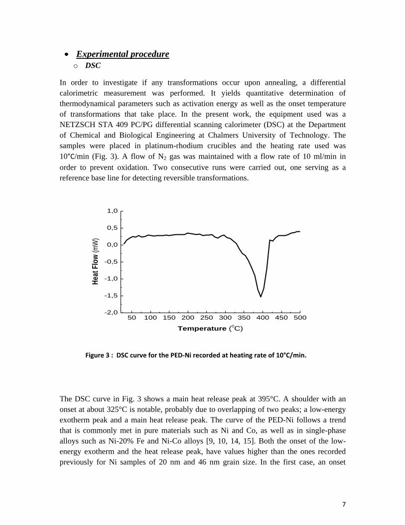
o DSC
In order to investigate if any transformations occur upon annealing, a differential
calorimetric measurement was performed. It yields quantitative determination of
thermodynamical parameters such as activation energy as well as the onset temperature
of transformations that take place. In the present work, the equipment used was a
NETZSCH STA 409 PC/PG differential scanning calorimeter (DSC) at the Department
of Chemical and Biological Engineering at Chalmers University of Technology. The
samples were placed in platinum-rhodium crucibles and the heating rate used was
10°C/min (Fig. 3). A flow of N2 gas was maintained with a flow rate of 10 ml/min in
order to prevent oxidation. Two consecutive runs were carried out, one serving as a
reference base line for detecting reversible transformations.
The DSC curve in Fig. 3 shows a main heat release peak at 395°C. A shoulder with an
onset at about 325°C is notable, probably due to overlapping of two peaks; a low-energy
exotherm peak and a main heat release peak. The curve of the PED-Ni follows a trend
that is commonly met in pure materials such as Ni and Co, as well as in single-phase
alloys such as Ni-20% Fe and Ni-Co alloys [9, 10, 14, 15]. Both the onset of the low-
energy exotherm and the heat release peak, have values higher than the ones recorded
previously for Ni samples of 20 nm and 46 nm grain size. In the first case, an onset
Figure 3 : DSC curve for the PED-Ni recorded at heating rate of 10°C/min.
50 100 150 200 250 300 350 400 450 500-2,0
-1,5
-1,0
-0,5
0,0
0,5
1,0
Hea
t F
low
(m
W)
Temperature (0C)
8
temperature of 84°C was determined, followed by a main peak at 289°C, while for the 46
nm material an onset temperature of 60°C and a main peak at 285°C was observed [7].
o Heat treatment
From the DSC curve alone it is not clear what type of transformations take place in the
temperature range of the low exotherm. Hence, complementary methods must be applied.
For that matter, heat treatments in a vacuum furnace were carried out on bulk samples
combined with an in-situ TEM annealing treatment on a thin foil. Furnace heat treatments
were performed at 350, 400, 450, 500, 550 and 650°C for 20 min. Then the samples were
left at room temperature for about 1 hour to cool down. For the in-situ TEM annealing, a
Gatan double-tilt heating holder with a tantalum furnace was used, which allows heating
up the sample to 1000°C. This technique allows the direct monitoring of transformations.
During the in-situ experiment, the temperature was raised in steps of 50 degrees from
200°C up to 600°C.
o EBSD
Electron Backscatter Diffraction (EBSD) is a technique which allows obtaining
crystallographic information from samples in the scanning electron microscope (SEM).
Both bulk samples and TEM foil were investigated. All measurements were performed
over an area of 22,6 x 17,2 μm (565 x 430 = 242950 pixels) (see appendix for details),
with step size of 0,040 μm. The electron beam scanned the samples at a direction parallel
to the growth direction (GD) of the electrodeposit. The Kikuchi diffraction patterns
acquired for each pixel are stored through a software application into a dataset file. Once
that is completed, it is possible to obtain information about local texture, grain boundary
misorientation and distribution, grain morphology and phase distribution. In this work, a
LEO Gemini 1550 FEG-SEM and a HKL Channel 5 EBSD system with Nordlys II
detector were used. Measurements were carried out at an acceleration voltage of 20 kV
and at a working distance of 17 mm.
o Sample preparation
All samples were prepared with respect to the cross-section of the material, i.e. parallel to
the growth direction of the electrodeposit. The bulk specimens were mechanically
polished with SiC papers down to grid size 4000 and subsequently electropolished using
a Struers Lectropol-5 with a Struers A2 electrolyte consisting of perchloric acid 60%, 2-
butoxyethanol, ethanol and distilled water. The TEM samples were prepared via dimple
grinding and ion milling. Discs of 3 mm in diameter were punched from thin (<150 μm in
thickness) sheets and then polished down to ~70 μm in thickness using 3 μm diamond
paste. Afterwards, a dimple was created in the center of the discs through mechanical
polishing on both sides using a Gatan model 656 dimple grinder with 3 μm and 1 μm
9
diamond pastes. Finally, ion milling was carried out with a Gatan precision ion polishing
system (PIPS) using an angle of incidence of 4°, until a hole was created in the middle.
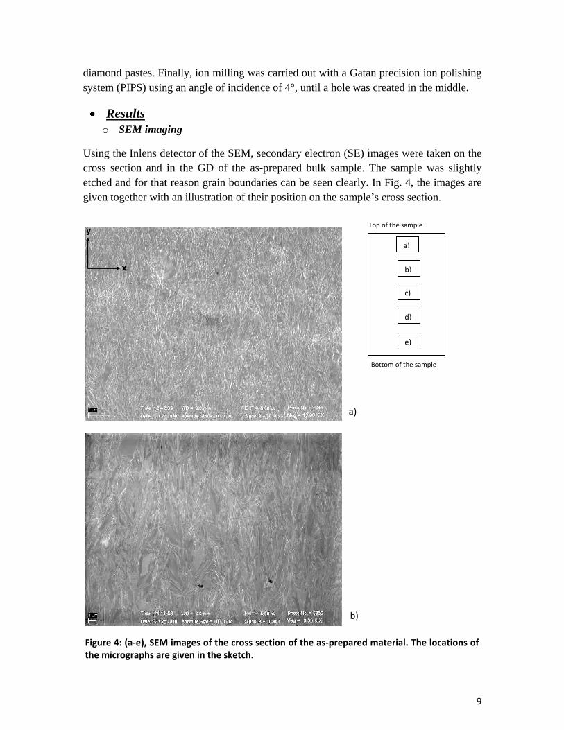
Results
o SEM imaging
Using the Inlens detector of the SEM, secondary electron (SE) images were taken on the
cross section and in the GD of the as-prepared bulk sample. The sample was slightly
etched and for that reason grain boundaries can be seen clearly. In Fig. 4, the images are
given together with an illustration of their position on the sample’s cross section.
Figure 4: (a-e), SEM images of the cross section of the as-prepared material. The locations of the micrographs are given in the sketch.
a)
b)
a)
b)
Bottom of the sample
Top of the sample
c)
d)
e)

10
c)
d)
e)
Figure 4: (a-e), SEM images of the cross section of the as-prepared material. The locations of the micrographs are given in the sketch.

11
SE images reveal the microstructure of the sample in the as-prepared state. From the
bottom to the top of the sample there is a notable change in the microstructure. At the
bottom of the sample (substrate side), few distinct elongated grains of approximately 2
μm in length are present (not taking into account the presence of any twin boundaries at
this point). These grains are oriented parallel to the GD of the sample, surrounded by
grains which are smaller in size. Away from the substrate the structure progressively
changes. That bimodal grain structure is becoming more apparent. The area fraction of
the elongated grains increases as they increase in number and in average length from the
bottom to the top of the sample. It can be noticed, more specifically in Figs. 2a, b and c,
that at the center and especially near the top of the sample the elongated grains have
maximum size and completely dominate the microstructure. The sample thus exhibits an
overall inhomogeneous structure.
o Orientation maps
In order to follow the development of the microstructure during the annealing sequence,
orientation maps were taken at each temperature. Inverse pole figure coloring was used
with respect to the three sample directions; the colour key which illustrates the grain
orientations in the respective crystallographic directions is given in Fig. 5. For all
orientation maps (Figs. 6 to 8) noise reduction was performed in order to increase the
hit rate of the measurements. First so-called wild spikes were removed. That is when the
adjacent 8 pixels of an indexed point are all not indexed or all indexed differently. Then,
orientation information was assigned to un-indexed points based on the orientation of 4
closest neighbor points which are equally indexed (see appendix for percentages).
Figure 5: Colour key for the different crystallographic orientations.

12
a)
Figure 6: Orientation maps with respect to the GD (parallel to Y axis) for a) as-prepared, b) 350°C, c) 400°C, d) 450°C, e) 500°C, f) 550°C, g) 600°C and h) 650°C (scale bar length equals to 10 μm).
b)
c) d)
e)
f)
g) h)
d)
h)
13
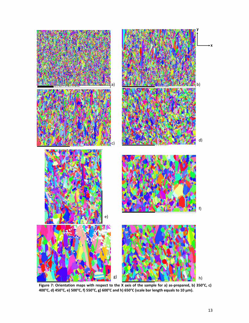
Figure 7: Orientation maps with respect to the X axis of the sample for a) as-prepared, b) 350°C, c) 400°C, d) 450°C, e) 500°C, f) 550°C, g) 600°C and h) 650°C (scale bar length equals to 10 μm).
b)
c) d)
e)
f)
g)
a) b)
h)
14
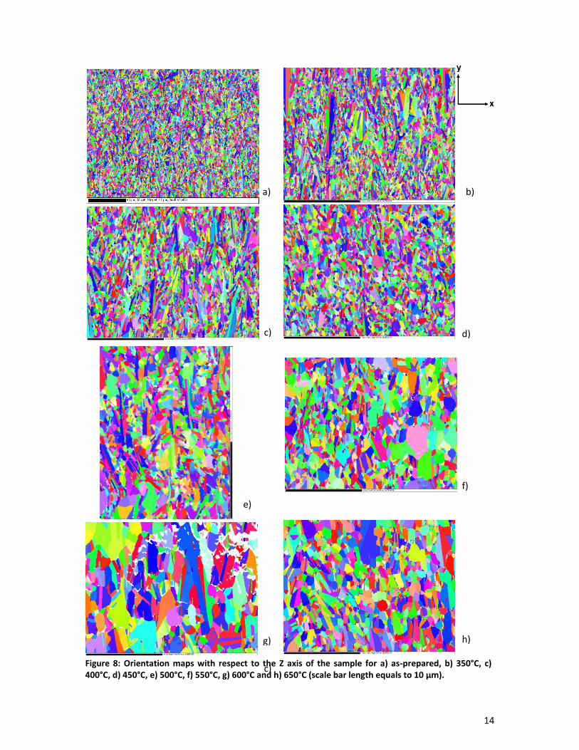
Figure 8: Orientation maps with respect to the Z axis of the sample for a) as-prepared, b) 350°C, c) 400°C, d) 450°C, e) 500°C, f) 550°C, g) 600°C and h) 650°C (scale bar length equals to 10 μm).
f)
h)
a)
b)
c)
d)
e)
g)
b)
c)
15
In all following analyses/discussions, the 650°C sample is excluded. During the
measurement of that sample, an effect due to pseudosymmetry occurred, altering the
information obtained. Thus, the measured data is not taken into account.
The orientation maps performed after annealing reveal in all cases a bimodal
inhomogeneous structure. The elongated grains that were already present from the
initial state are present throughout the whole annealing process. Those grains are in
their majority <110> oriented parallel to the GD of the sample. With increasing
annealing temperature, the elongated grains become more dominant as they increase in
area size and elongation. These elongated grains are surrounded by smaller grains of
different shapes and orientations. As the annealing temperature increases the small
grains grow and tend to keep a more round shape, as it can best be seen in the sample
annealed at 600°C.
In the following curves, the values between initial state of the material (i.e. 65°C) and
the different heat treatment temperatures (i.e. 350, 400, 450, 500, 550 and 600°C) are
extrapolated and not actually measured for that temperature interval.
o Grain size and area determination
Regarding the average size and area of grains, the calculations were performed based on
a minimum misorientation angle between the boundaries of neighbor grains. Incomplete
grains that exist at the borders of the map were excluded from the analysis. Average
grain size was obtained by two methods: with the “equivalent circle diameter” method
which calculates the diameter of a circle of the same size (Fig. 9) and “line intercept”
method which measures distances (i.e. grain diameters) both parallel and perpendicular
directions to the GD (Fig. 10). The area size of the grains is then calculated by
multiplying the number of pixels in each grain with the pixel size (Fig. 11). In these
analyses, both high angle grain boundaries (HAGBs) with θ above 15° and low angle
grain boundaries (LAGBs) with θ between 3° and 15° were taken into account.
An average grain size of 145 nm is measured with the “equivalent circle diameter”
method in the initial state that progressively increases to 195 nm at 400°C. Between
400°C and 600°C, the grain size is more rapidly increasing and reaches a maximum
value of 347 nm at 600°C (Fig. 9).

16
Figure 9: Average grain size obtained with “equivalent circle diameter” method
Using the “line intercept” method the average size of the grains in the GD is increasing
from 170 nm in the initial state to 248 nm at 400°C. Perpendicular to the GD the average
grain size increases from 120 nm at the initial state to 143 nm at 400°C. Between 400°C
and 600°C, a more rapid increase in the average grain size with temperature is noticed.
The average size increases from 248 nm to a maximum of 761 nm when measured
parallel to the GD. Measuring perpendicular to the GD, an increase to the average grain
size from 143 nm at 400°C to 484 nm at 600°C is observed (Fig. 10).
Figure 10: Average grain size obtained with “line intercept” method both in parallel and perpendicular to GD
0
0,05
0,1
0,15
0,2
0,25
0,3
0,35
0,4
65 350 400 450 500 550 600
Minimum boundary angle misorientation of 3 degrees
Temperature °C
Gra
in s
ize
aver
age
(μm
)
0
0,1
0,2
0,3
0,4
0,5
0,6
0,7
0,8
65 350 400 450 500 550 600
Perpendicular to the GD
Parallel to the GD
Temperature °C
Gra
insi
ze a
vera
ge (μ
m)
17
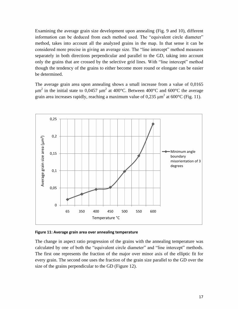
Examining the average grain size development upon annealing (Fig. 9 and 10), different
information can be deduced from each method used. The “equivalent circle diameter”
method, takes into account all the analyzed grains in the map. In that sense it can be
considered more precise in giving an average size. The “line intercept” method measures
separately in both directions perpendicular and parallel to the GD, taking into account
only the grains that are crossed by the selective grid lines. With “line intercept” method
though the tendency of the grains to either become more round or elongate can be easier
be determined.
The average grain area upon annealing shows a small increase from a value of 0,0165
μm2 in the initial state to 0,0457 μm
2 at 400°C. Between 400°C and 600°C the average
grain area increases rapidly, reaching a maximum value of 0,235 μm2 at 600°C (Fig. 11).
Figure 11: Average grain area over annealing temperature
The change in aspect ratio progression of the grains with the annealing temperature was
calculated by one of both the “equivalent circle diameter” and “line intercept” methods.
The first one represents the fraction of the major over minor axis of the elliptic fit for
every grain. The second one uses the fraction of the grain size parallel to the GD over the
size of the grains perpendicular to the GD (Figure 12).
0
0,05
0,1
0,15
0,2
0,25
65 350 400 450 500 550 600
Minimum angle boundary misorientation of 3 degrees
Temperature °C
Ave
rage
grai
n s
ize
area
(μ
m²)

18
Figure 32: Aspect ratio of grains upon annealing temperature
The cause of the discrepancy in values (Fig. 12) is due to the fact that each curve is
calculated based on different methods. In one case we have the ratio calculated based on
the “elliptic fit” method while on the other is done based on “line intercept” method. As
explained earlier these two methods differ in the number of grains measure and the way
grain size is measured.
Figure 43: In-situ TEM annealing at a) 550°C for 20 min and b) 600°C for 20min.
0
0,5
1
1,5
2
2,5
3
65 350 400 450 500 550 600
Aspect ratio with elliptic fit
Aspect ratio with line intercept
Temperature °C
Asp
ect
rati
o

19
Using in-situ annealing in TEM, it was possible to isolate grains and monitor their
evolution with increasing temperature. Two typical examples of grown grains are given
in Figs. 13 and 14 where the same location is seen at different annealing temperatures
(500°C and 600°C).
Figure 54: In-situ TEM annealing at a) 550°C for 20 min and b) 600°C for 20 min.
a) b)
1 μm
20
From the average grain size and average grain area curves (Figs. 9 - 11) it is obvious that
significant grain growth takes place between 400°C and 600°C. From 450°C to 500°C
(judging from Fig. 12) the grains seem to have gained more in width rather than in
elongation in the respective annealing steps. However, this also could be attributed to the
inhomogeneity of the microstructure. Another similar observation can be pointed out
between 400°C and 450°C (Figs 9 and 11). At these annealing temperatures, grains seem
to grow not as much as in the previous or in the following annealing steps.
Following the average aspect ratio progression of the grains with temperature (Fig. 12), it
appears as if the grains tend to become more round after 400°C. At 500°C the aspect ratio
assumes a relatively low value that appears different compared to the general trend of the
curve. This has already been mentioned to be attributed to the inhomogeneity of the
microstructure. At 550°C and 600°C, the aspect ratio again shows a minor increase in
value. This is due to the fact that at these temperatures grains have grown significantly in
size. Big elongated grains with high aspect ratio dominate now the microstructure. Thus,
when examining the same area upon annealing, an increase in the overall average aspect
ratio values is expected. The elongated grains as seen in the TEM (Fig. 14) appear stable
with increasing temperature and grew in length instead of width.
21
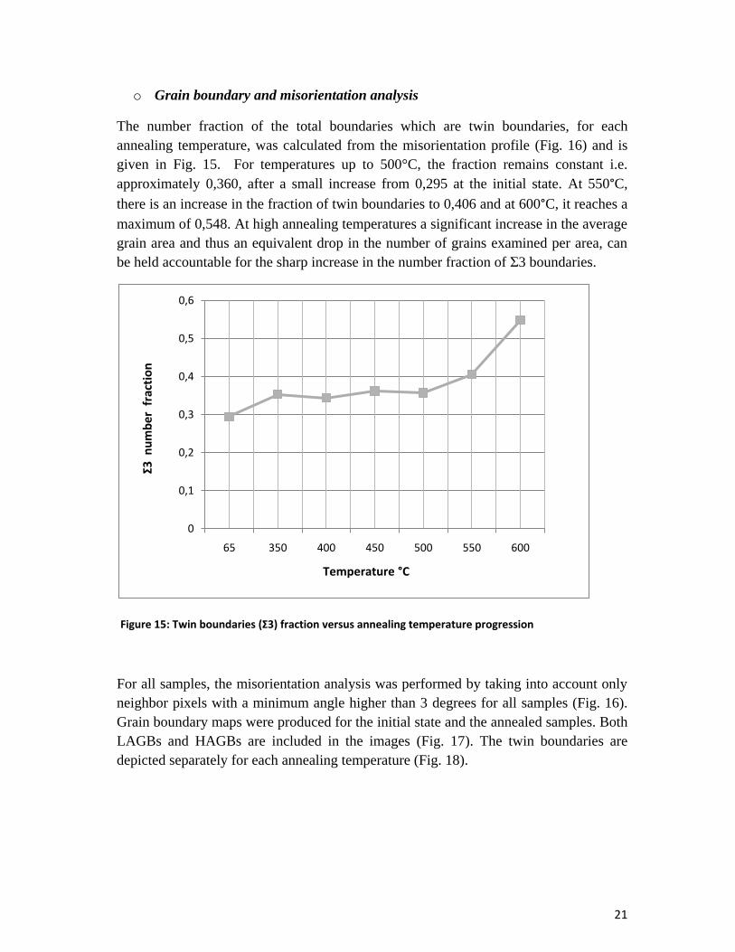
o Grain boundary and misorientation analysis
The number fraction of the total boundaries which are twin boundaries, for each
annealing temperature, was calculated from the misorientation profile (Fig. 16) and is
given in Fig. 15. For temperatures up to 500°C, the fraction remains constant i.e.
approximately 0,360, after a small increase from 0,295 at the initial state. At 550°C,
there is an increase in the fraction of twin boundaries to 0,406 and at 600°C, it reaches a
maximum of 0,548. At high annealing temperatures a significant increase in the average
grain area and thus an equivalent drop in the number of grains examined per area, can
be held accountable for the sharp increase in the number fraction of Σ3 boundaries.
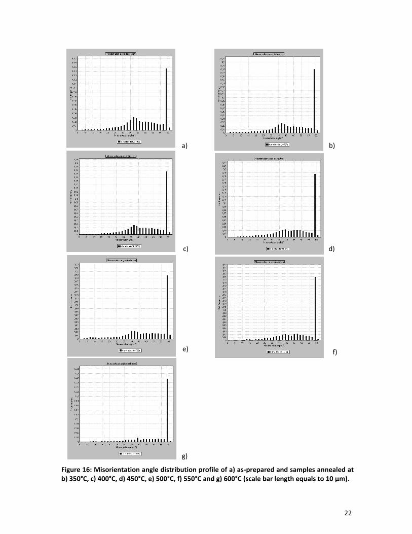
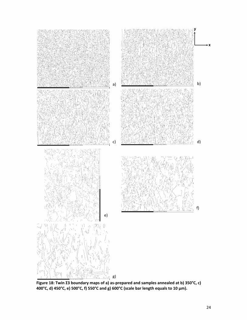
For all samples, the misorientation analysis was performed by taking into account only
neighbor pixels with a minimum angle higher than 3 degrees for all samples (Fig. 16).
Grain boundary maps were produced for the initial state and the annealed samples. Both
LAGBs and HAGBs are included in the images (Fig. 17). The twin boundaries are
depicted separately for each annealing temperature (Fig. 18).
0
0,1
0,2
0,3
0,4
0,5
0,6
65 350 400 450 500 550 600
Σ3 n
um
be
r f
ract
ion
Temperature °C
Figure 15: Twin boundaries (Σ3) fraction versus annealing temperature progression
22
Figure 16: Misorientation angle distribution profile of a) as-prepared and samples annealed at b) 350°C, c) 400°C, d) 450°C, e) 500°C, f) 550°C and g) 600°C (scale bar length equals to 10 μm).
a) b)
c) d)
e)
f)
g)
f)

23
Figure 17: GBs maps of a) as-prepared and samples annealed at b) 350°C, c) 400°C, d) 450°C, e) 500°C, f) 550°C and g) 600°C (scale bar length equals to 10 μm).
a) b)
c) d)
e)
f)
g)
24
c)
a)
b)
d)
e)
f)
g)
Figure 18: Twin Σ3 boundary maps of a) as-prepared and samples annealed at b) 350°C, c) 400°C, d) 450°C, e) 500°C, f) 550°C and g) 600°C (scale bar length equals to 10 μm).
b)
f)

25
o Texture analysis
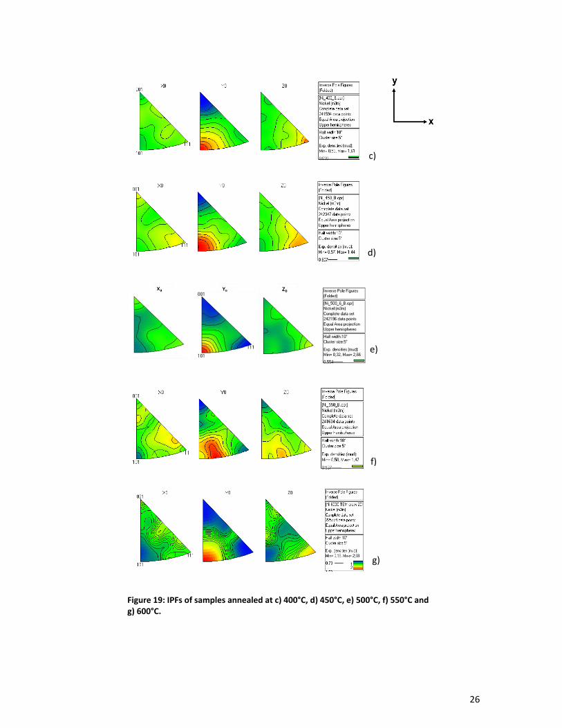
Inverse pole figures (IPF) were obtained for the different samples (Fig. 19). The GD for
all samples is parallel to the Y axis. During the whole annealing treatment sequence, the
texture remains <110> // GD but exhibits minor changes in intensity values throughout
the sequence. A minimum value of 1,3 is found in the as-prepared state while a
maximum value of 2,68 is reached at 600°C.
In the Z-direction, a weak <111> texture is present throughout the whole annealing
sequence. Again, intensity is changing in a similar manner to that parallel to the GD. At
the initial state, intesity it has the lowest value of 1,1 and reaches its maximum value of
2,04 at 600°C.
The minor fluctuations in intensity and the slight deviation from <100> // GD at 550°C
can be attributed to the inhomogeneity of the sample’s microstructure. Since the <110>
fibre texture parallel to the GD is present at all annealing steps before and after 550°C,
it is safe to assume that the reason for this deviation is due to the choice of the sample’s
location.
a)
b)
Figure 19: IPFs of a) as-prepared state and samples annealed at b) 350°C.
26
c)
d)
e)
f)
g)
Figure 19: IPFs of samples annealed at c) 400°C, d) 450°C, e) 500°C, f) 550°C and g) 600°C.

27
o Subset / anti-subset analysis
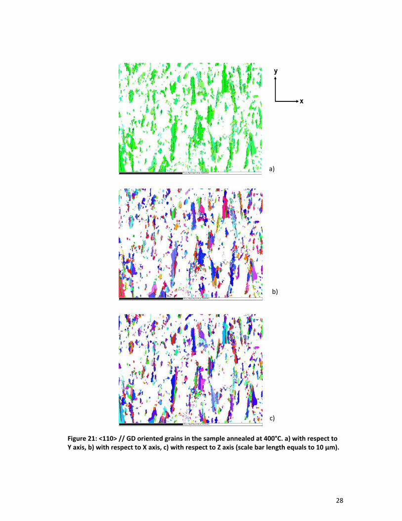
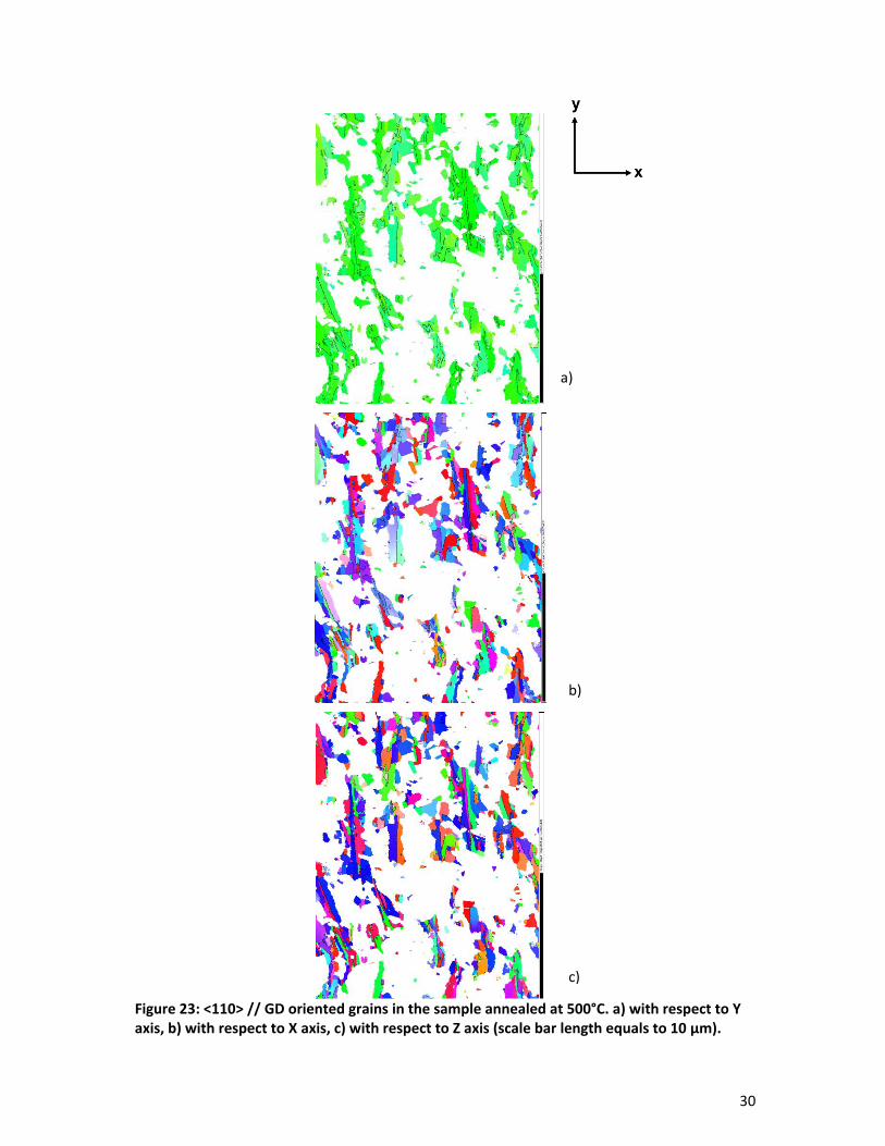
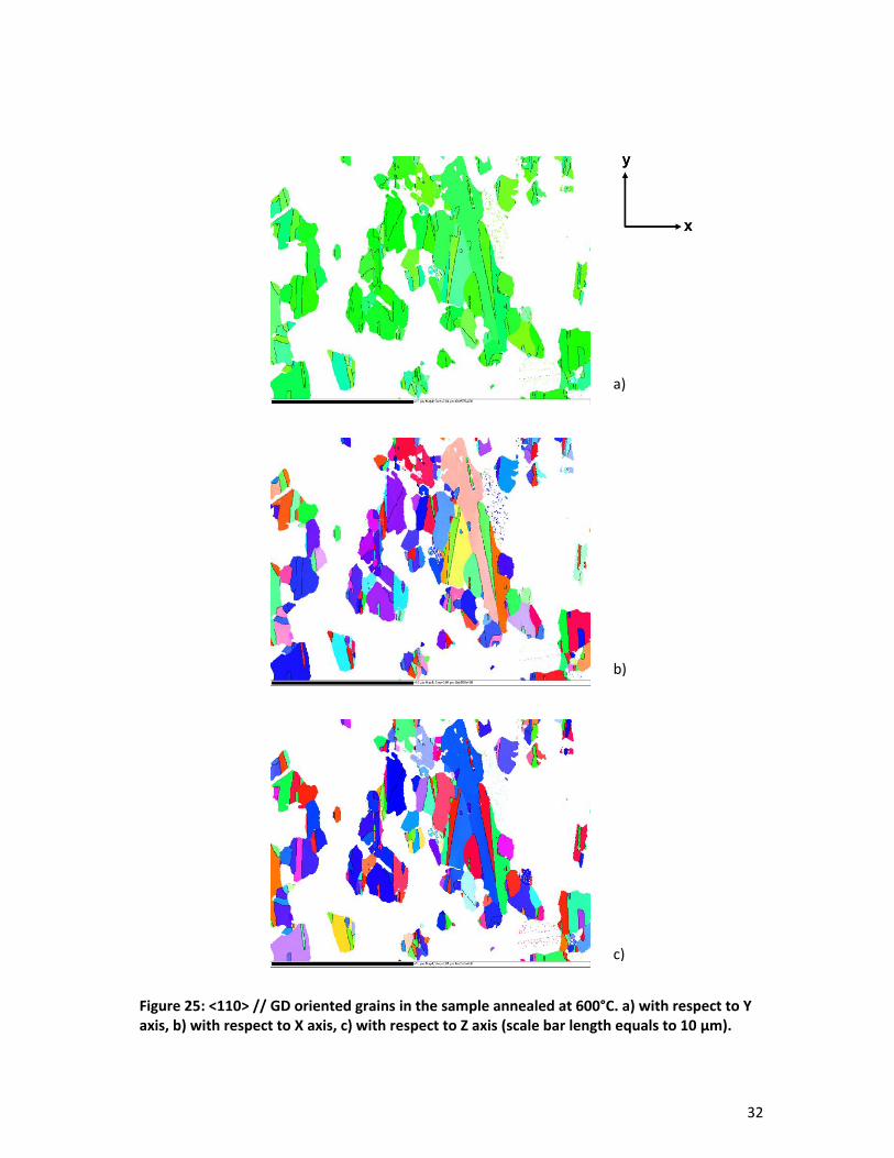
Subsets were created for all samples to examine the dominant <110> texture along the
GD axis. A minimum deviation angle of 15° from that axis was chosen. Each map is
depicted with IPF colour code with respect to the sample axes (Fig. 20 to 25). Twin
boundaries are also included in the images.
a)
b)
c)
Figure 20: <110> // GD oriented grains in the sample annealed at 350°C. a) with respect to Y axis, b) with respect to X axis, c) with respect to Z axis (scale bar length equals to 10 μm).
28
Figure 21: <110> // GD oriented grains in the sample annealed at 400°C. a) with respect to Y axis, b) with respect to X axis, c) with respect to Z axis (scale bar length equals to 10 μm).
a)
b)
c)

29
Figure 22: <110> // GD oriented grains in the samples annealed at 450°C. a) with respect to Y axis, b) with respect to X axis, c) with respect to Z axis (scale bar length equals to 10 μm).
a)
b)
c)
30
Figure 23: <110> // GD oriented grains in the sample annealed at 500°C. a) with respect to Y axis, b) with respect to X axis, c) with respect to Z axis (scale bar length equals to 10 μm).
a)
b)
c)

31
Figure 24: <110> // GD oriented grains in the sample annealed at 550°C. a) with respect to Y axis, b) with respect to X axis, c) with respect to Z axis (scale bar length equals to 10 μm).
a)
b)
c)
32
Figure 25: <110> // GD oriented grains in the sample annealed at 600°C. a) with respect to Y axis, b) with respect to X axis, c) with respect to Z axis (scale bar length equals to 10 μm).
a)
b)
c)

33
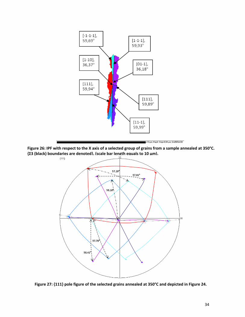
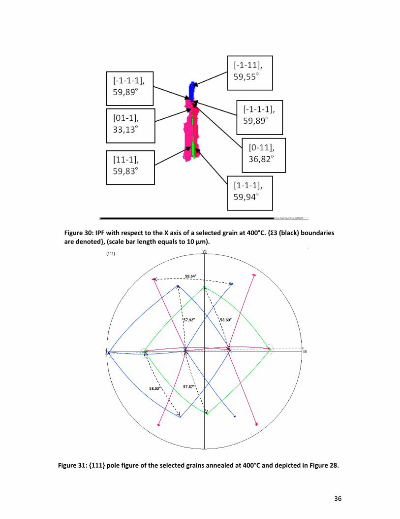
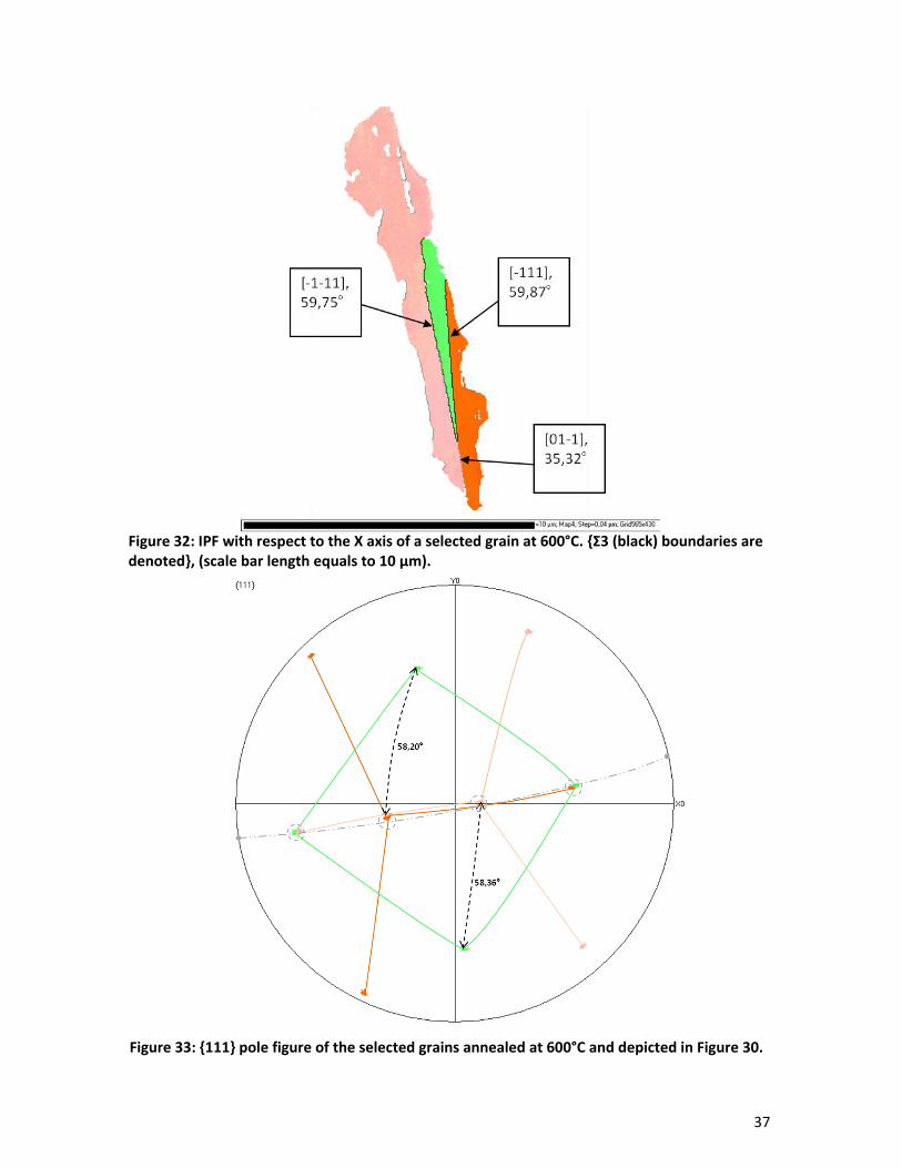
The importance of twin boundaries in the evolution of the microstructure and texture
during annealing treatment may be best seen with a more detailed investigation of
isolated grain groups. Thus, different subset groups from the IPF maps were created.
Among the <110> grains there are certain groups of grains that appear more frequently
throughout the annealing steps. Some of these points of interest are being isolated and
studied further. IPF orientation maps of these groups of grains and their respective pole
figures were acquired (Figs. 26 - 33).
The group of grains seen in Figs. 20 - 25 form patterns easily distinguishable
throughout the samples. With respect to the Y axis (parallel to the GD) the grouped
grains always have <110> // GD orientation. The groups of grains can be found in either
small or large size at all annealing temperatures. Twin relationships are always observed
between them. Upon twinning, a <110>//GD oriented grain can provide another
<110>//GD oriented grain. Hence, twinning and the formation of these distinct groups
of grains, which are in addition often occur as long, elongated grains, leads to the
dominant <110>//GD texture upon annealing. Also Σ9 boundaries are observed in
between junctions of Σ3 forming Σ3-Σ3-Σ9 patterns. When inspecting these groups of
grains in IPF orientation maps with respect to X axis, some distinct colour combinations
appear. These colour combinations are translated through the colour key code to defined
orientations. Most often, combinations of purple – blue – red, or orange – pink – green,
or pink – blue - green occur. The reason for these variations is because the groups of
grains have different misorientations with the GD of the sample. This can be seen in the
pole figures (Fig. 27, 29, 31, 33). The twin axes of the group of grains lie along the
equator or form a small angle with it. Hence, the twin boundaries are more or less
aligned with the GD.
34
Figure 26: IPF with respect to the X axis of a selected group of grains from a sample annealed at 350°C. {Σ3 (black) boundaries are denoted}, (scale bar length equals to 10 μm).
Figure 27: {111} pole figure of the selected grains annealed at 350°C and depicted in Figure 24.

35
Figure 28: IPF with respect to the X axis of a selected group of grains from a sample annealed at 350°C. {Σ3 (black) boundaries are denoted}, (scale bar length equals to 10 μm).
Figure 29: {111} pole figure of the selected grains annealed at 350°C and depicted in Figure 26.
36
Figure 30: IPF with respect to the X axis of a selected grain at 400°C. {Σ3 (black) boundaries are denoted}, (scale bar length equals to 10 μm).
Figure 31: {111} pole figure of the selected grains annealed at 400°C and depicted in Figure 28.
37
Figure 32: IPF with respect to the X axis of a selected grain at 600°C. {Σ3 (black) boundaries are denoted}, (scale bar length equals to 10 μm).
Figure 33: {111} pole figure of the selected grains annealed at 600°C and depicted in Figure 30.

38
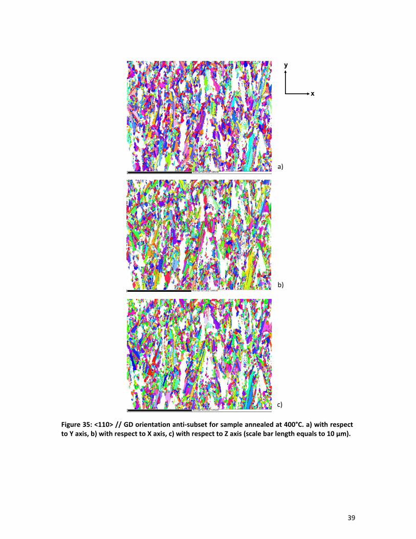
IPF orientation maps of the <110> anti-subsets with respect to the sample axes are
given in Figs. 34 - 39. Twin boundaries are also included in the images.
Figure 34: <110> // GD orientation anti-subset for sample annealed at 350°C. a) with respect to Y axis, b) with respect to X axis, c) with respect to Z axis (scale bar length equals to 10 μm).
a)
b)
c)
39
a)
b)
c)
Figure 35: <110> // GD orientation anti-subset for sample annealed at 400°C. a) with respect to Y axis, b) with respect to X axis, c) with respect to Z axis (scale bar length equals to 10 μm).

40
Figure 36: <110> // GD orientation anti-subset for sample annealed at 450°C. a) with respect to Y axis, b) with respect to X axis, c) with respect to Z axis (scale bar length equals to 10 μm).
a)
b)
c)

41
Figure 37: <110> // GD orientation anti-subset for samples annealed at 500°C. a) with respect to Y axis, b) with respect to X axis, c) with respect to Z axis (scale bar length equals to 10 μm).
a)
b)
c)
42
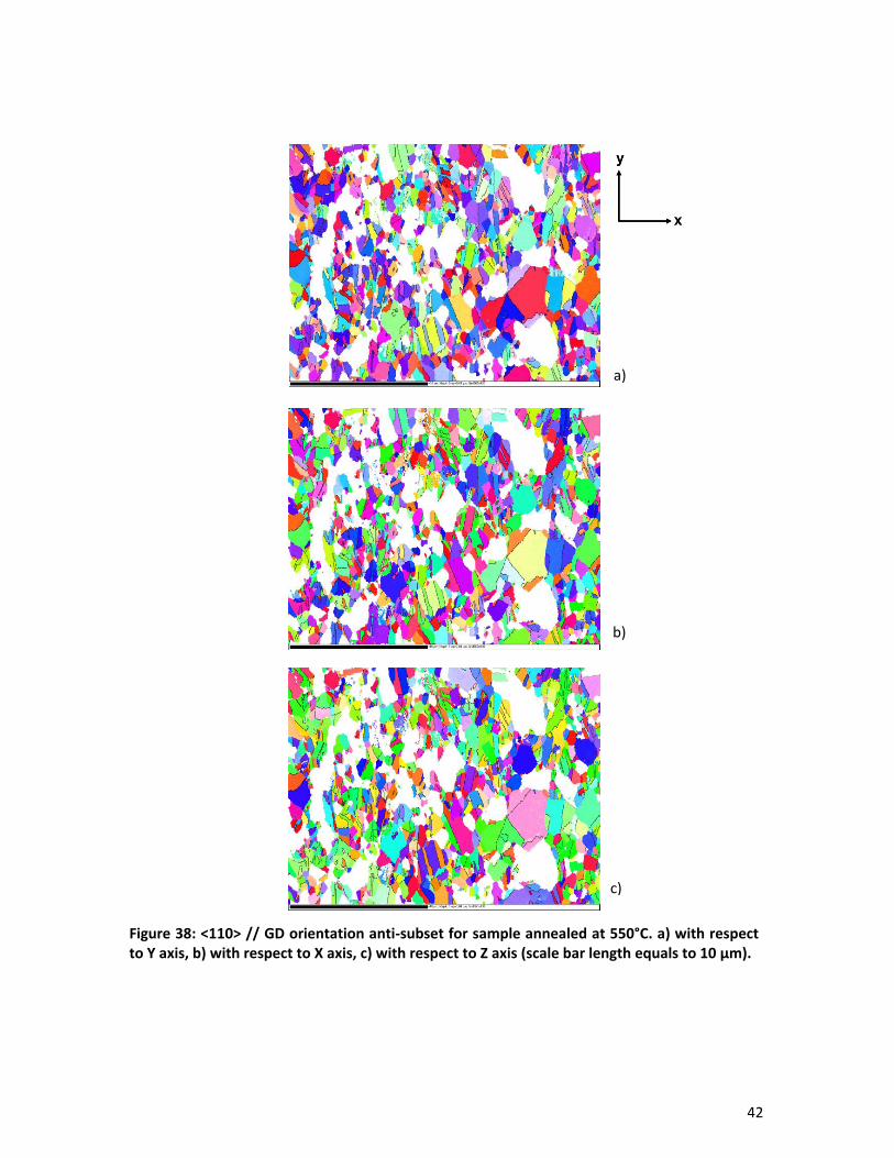
Figure 38: <110> // GD orientation anti-subset for sample annealed at 550°C. a) with respect to Y axis, b) with respect to X axis, c) with respect to Z axis (scale bar length equals to 10 μm).
a)
b)
c)
43
a)
b)
c)
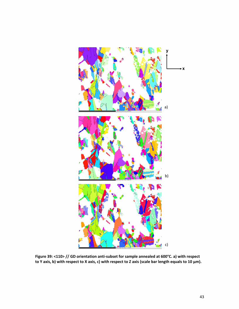
Figure 39: <110> // GD orientation anti-subset for sample annealed at 600°C. a) with respect to Y axis, b) with respect to X axis, c) with respect to Z axis (scale bar length equals to 10 μm).
44
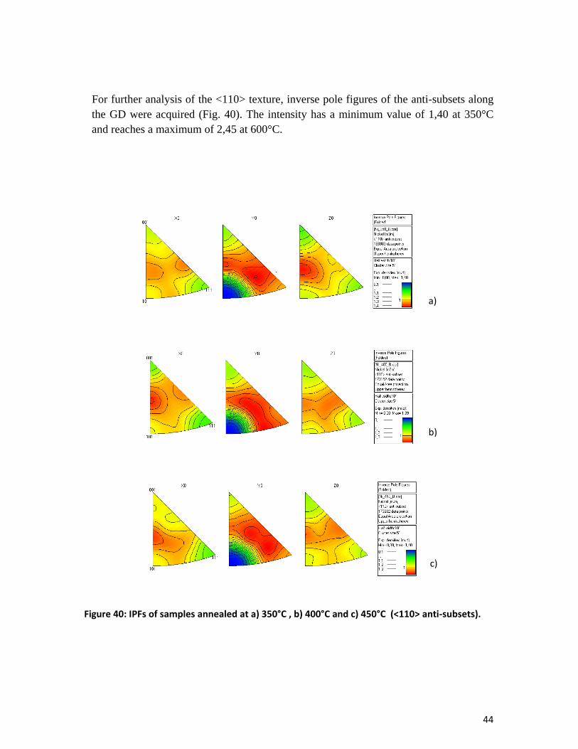
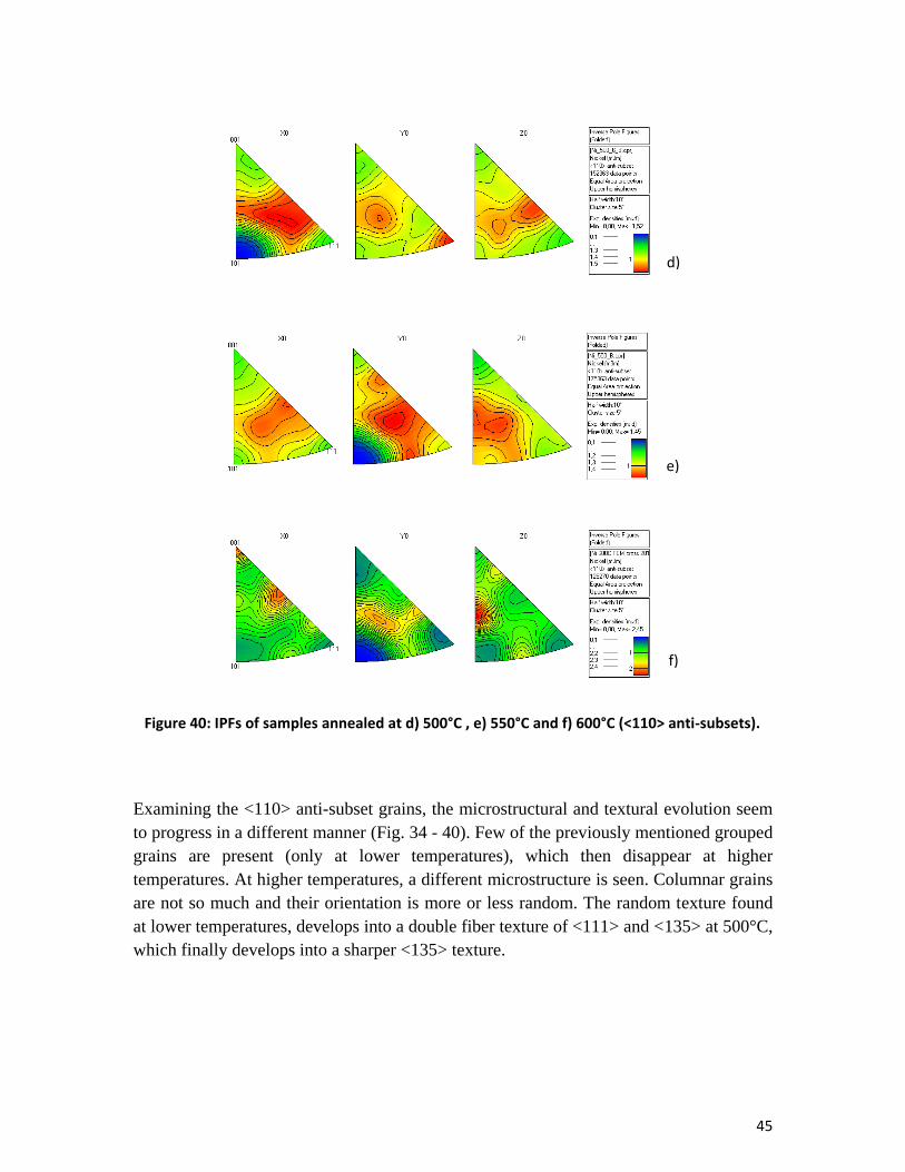
For further analysis of the <110> texture, inverse pole figures of the anti-subsets along
the GD were acquired (Fig. 40). The intensity has a minimum value of 1,40 at 350°C
and reaches a maximum of 2,45 at 600°C.
Figure 40: IPFs of samples annealed at a) 350°C , b) 400°C and c) 450°C (<110> anti-subsets).
a)
b)
c)
45
Examining the <110> anti-subset grains, the microstructural and textural evolution seem
to progress in a different manner (Fig. 34 - 40). Few of the previously mentioned grouped
grains are present (only at lower temperatures), which then disappear at higher
temperatures. At higher temperatures, a different microstructure is seen. Columnar grains
are not so much and their orientation is more or less random. The random texture found
at lower temperatures, develops into a double fiber texture of <111> and <135> at 500°C,
which finally develops into a sharper <135> texture.
Figure 40: IPFs of samples annealed at d) 500°C , e) 550°C and f) 600°C (<110> anti-subsets).
f)
d)
e)

46
Discussion
The findings regarding the microstructure of the PED Ni in the present work are in good
agreement with those mentioned in literature. Due to the absence of any kind of additives
and alloying additions, the presence of columnar grains is well expected. Also the
bimodal type of microstructure with small-sized grains dispersed in between the
elongated ones is in accordance with the literature [20, 24]. The size of the elongated
grains increases with plating thickness, a trend which also has been seen before on Ni
EDs [19, 25]. The temperature of the plating bath is influencing the microstructure and
the formation of elongated grains. The higher temperature of the electrolytic bath used for
plating the material analyzed in this work (65°C compared to what is found in the
literature e.g. 28°C, 30°C, 50°C [19, 16, 24]), is also a reason for the increased size of the
columnar grains. But the temperature of the electrolytic bath is not the sole parameter that
affects the grain size. However, it can be indicative. The low current density of 2 A/dm2
used is also contributing to the fact that the grains are not in the nanometer but rather in
the sub-micrometer range [19]. Finally, also the pH value of 4,2 is within the range in
which columnar grains develop.
In contrast to the microstructure, the <110> texture along the GD is not frequently
observed in nanocrystalline Ni EDs. Usually, a (200)/(111) double fibre texture is more
common [7, 8, 9, 13]. The <110> texture it is common for EDs of columnar structure and
grain size in the sub-micrometer range [11, 12, 15, 16, 20, 21, 22, 23, 24, 25]. The current
density value as shown can be hold responsible for the development of the texture [10,
11, 13]. For the Ni electrodeposit under investigation, the current density used should
yield <100> texture under d.c conditions [10, 11, 12]. Pulse current is proven though to
perturb the texture evolution away from what is expected under d.c. conditions,
depending on the wave form of the current [12, 13]. Thus, for the <110> texture observed
at the present work the square-wave current form can be hold responsible. Furthermore
the high temperature was noted as an important factor that changes an initially <100> to
<110> for Ni EDs [16].
Randle et al [32] studied the evolution of annealing twins as a function of annealing
temperature. Commercially pure Nickel (99,5% Ni) samples with equiaxed grain
structure and average grain size of 30.2 μm were used. The results indicated that after a
certain value of Σ3 length fraction was established it was not changed further by grain
growth, implying that twinning has its own kinetics and can take place independently of
grain growth. In the present work, a similar behavior is seen: the number fraction of twin
boundaries remains constant for different annealing temperatures. The length fraction
though appears to increase with annealing temperature. The grains tend to elongate

47
mostly parallel to the twinning plane, rather than assume an equiaxed shape that would
favor the stability of the length fraction.
Grains having a <110> texture with respect to the GD and forming small colonies with
twin relationships in-between them were reported in previous studies [11, 23, 27]. For
Co-Ni EDs, Bastos et al [27] described the combination of a coherent twin, an incoherent
twin and a conventional large-angle grain boundary, all of them related to each other by a
rotation around a <11-20> axis. In the present study, the grains are related to each other
by 60° <111> orientation relationships. The grain boundaries between the grains in the
colonies are Σ3, low-angle boundaries and other general high-angle boundaries, all
sharing a common zone axis perpendicular to the GD. In previous studies the zone axis of
such relationships between grain boundaries were shown to be parallel to the GD. The
difference lies to the fact that the present study was conducted at the cross section of the
material, while the previous ones on the planar section. TEM investigations revealed that
upon annealing, the twin related columnar grains keep the initially grain arrangement and
grow rather in length than in width.
The presence of the large columnar grains is very likely to be the reason for the higher
thermal stability of the material, which is visible as a shift of the heat release peak to
higher temperature in the DSC curve. Their increased length i.e. about 2μm in average
and their stable arrangement, lead to a reduction of the driving force for grain growth as
compared to nanocrystalline material. That the larger grain size are responsible for the
improved thermal stability is also supported by the fact that due to the high purity of the
material, no other stabilizing mechanisms are active such as solute drag, Zener drag or
segregation [7, 8].
The presence of additives or alloy elements has shown to change the texture of Ni EDs
upon annealing. Saccharin for instance has proven to change the texture into a <111>
fibre texture parallel to the GD [22, 33]. Ni-Fe EDs showed the same result, that means a
final texture of <111> upon annealing, while Ni-Mn EDs changed from an initial <110>
fibre texture parallel to the GD to a final <√310> texture upon annealing at 600°C [33,
24]. Nickel EDs though with columnar structure in the submicro-crystalline region, have
been reported to be more stable, i.e. they keep their initial texture.
In an in-situ TEM annealing treatment of the same material (the TEM foil prepared in
planar section was annealed up to 600°C [34]), a transition from the initial <110> fibre
texture to a <100> <111> double fibre textures parallel to the GD was observed. This
transition was not found in the present work. This is probably due to the different ways
the samples were prepared. In the present study, both bulk samples and thin foil agree
texture wise. The consistency of the texture throughout the whole annealing treatment
can be attributed to the presence of the twin boundaries between the long columnar
48
grains. From the TEM images it can be seen that the Σ3 boundaries inhibit further growth
in width and preserve the initial <110> texture parallel to the GD.
Conclusions and future work
In the present work, microstructure and texture of pulsed electrodeposited Nickel was
investigated in as-prepared state and after different annealing treatments. Results were
compared with other Nickel-based EDs from the literature. The material under
investigation exhibits a bimodal structure in which columnar grains of the order of sub-
micrometer dominate the otherwise nanometer-sized grain structure. This type of
microstructure is common among EDs and its appearance is strongly depended on the
electrodeposition parameters. The material exhibits a fibre texture of <110> parallel to
the GD which is preserved also at high annealing temperatures. A high number fraction
of Σ3 boundaries is present at all annealing temperatures. Columnar grains of the same
orientation parallel to the GD related to each other by twinning form stable colonies of
grains upon annealing. These twin colonies are responsible for the microstructure and
texture evolution of the EDs at elevated temperatures.
More dedicated microscopy could highlight the importance of these twin related grain
colonies upon annealing. EBSD investigations of the planar section of the material at
elevated temperatures would contribute to the fully description of the microstructural and
texture development. An EBSD map over the whole cross-section the sample and TEM
investigations in as-prepared state would also reveal more information on the
microstructural development and how it is affected by the plating parameters.
49
References
[1] U. Erb; NanoStructured Mat., Vol. 6, pp. 533-538, (1995).
[2] C. Suryanarayana and C.C. Koch; Hyperfine Interactions 130: 5–44, (2000).
[3] Don Baudrand; Metal Finishing, 94 (7), pp. 15 – 18, (1996).
[4] U. Erb, A. M. El-Sherik (1994) Patent: Nanocrystalline Metals and Process of
Producing the Same. US5352266.
[5] H. Gleiter, Prog. Mater. Sci. 33, 224 (1989).
[6] U. Erb, A.M. El-Sherik, G. Palumbo and K.T. Aust; NanoStructured Mat., Vol. 2,
pp. 383-390, (1993).
[7] M. da Silva and U. Klement; Z. Metallkd. Vol. 9, p. 1009, (2005).
[8] G.D. Hibbard, K.T. Aust, U. Erb; Materials Science and Eng., A 433, pp. 195-
202, (2006).
[9] U. Klement, U. Erb, A.M. El-Sherik, K.T. Aust; Materials Science and Eng., A
203, pp. 177-186, (1995).
[10] J. Amblard, M. Froment; Faraday Symposia of the Chemical Society 12, pp.
136-144, (1977).
[11] J. Amblard, I. Epelboin, M. Froment, G. Maurin; Journal of Applied
Electrochemistry 9 (2), pp. 233-242, (1979).
[12] C. Kollia, N. Spyrellis; Surface and Coatings Technology, 57, pp. 71-75, (1993).
[13] A.M. El-Sherik, U. Erb, J. Page; Surface and Coatings Technology 88, pp. 70-
78, (1996).
[14] A.M. El-Sherik, U. Erb; Journal of Materials Science 30, pp. 5743-5749, (1995).
[15] C. Bergenstof Nielsen, A. Horsewell, M. J. L. Østergård; Journal of Applied
Electrochemistry 27, pp. 839-845, (1997).
[16] S.H. Goods, J. J. Kelly, A.A. Talin, J. R. Michael, R. M. Watson; Journal of
Electrochemical Society, 153(5), C325-C331, (2006).
[17] F. Ebrahimi, Z. Ahmed; Materials Characterization 49, pp. 373-379, (2003).
[18] V.M. Kolzov, L. Peraldo Bicelli; Materials Chemistry and Physics 77, pp. 289-
293, (2002).
[19] A. A. Rasmussen, P. Møller, M. A. J. Somers; Surface and Coatings Technology
200, pp. 6037-6046, (2006).
[20] A. Bastos, S. Zaefferer, D. Raabe, C. Schuh; Acta Materialia 54, pp. 2451-2462,
(2006).
[21] A. Shibata, H. Noda, M. Sone, Y. Higo; Thin Solid Films 518, pp. 5153-5158,
(2010).
[22] J.J. Kelly and N.Y.C. Yang; SAND2001-8609, Unlimited release, Oct. 2001.
[23] G. Lucadamo, D.L. Meldin, N.Y.C. Yang, J.J. Kelly, A.A. Talin; Philosophical
Magazine, Vol. 85, No. 22, pp. 2549-2560, 1st August 2005.
50
[24] A.A. Talin, E.A. Marquis, S.H. Goods, J.J. Kelly, M.K. Miller; Acta Materialia
54, pp. 1935-1947, (2006).
[25] S.W. Banovic, K. Barmak, A.R. Marder; Journal of Materials Science 33, pp.
639-645, (1998).
[26] F. Ebrahimi, Z. Ahmed; Journal of Applied Electrochemistry 33, pp. 733-739,
(2003).
[27] A. Bastos, S. Zaefferer, D. Raabe; Journal of Microscopy, Vol. 230, Pt 3 2008,
pp. 487-498.
[28] Guan-Tai Lui, Delphic Chen, Jui-Chao Kuo; J. Phys. D: Appl. Phys. 42 (2009)
215410 (8pp).
[29] Stephan Armyanov; Electrochimica Acta 45 (2000) 3323-3335.
[30] Rolf Weil, Keith Sheppard; Mat. Characterization 28:103-112 (1992).
[31] J. Dille, J. Charlier, R. Winand; Journal of materials Science 32, pp. 2637-2646,
(1997).
[32] V. Randle, P.R. Rios, Y. Hu; Scripta Materialia 58 (2008), pp. 130-133.
[33] U. Klement, M. Da Silva & W. Skrotzki; Journal of Microscopy, Vol. 230, Pt 3
(2008), pp. 455-463.
[34] U. Klement, L. Hollang, R. Dey Suhash, M. Battabyal, O. V. Mishin, W.
Skrotzki; Diffusion and Defect Data Pt.B: Solid State Phenomena 160, pp. 235-
240 (2010).

51
ACKNOWLEDGEMENTS
This thesis has been a tremendously valuable experience and a great school for me. Many
important lessons learned and many tools I have gained that I know will prove to be
decisive in my future efforts. For those reasons I can only be grateful and I would like to
express my deeply gratitude and respect to all those who more or less helped me in
accomplishing this task. In particular I would like to thank the following:
My master program coordinator, Professor Jari Kinaret, is acknowledged for giving me
the opportunity to study in such high profile institute as Chalmers University of Sweden.
It was a life changing experience for me.
My supervisor and examiner of my master thesis, Professor Uta Klement, is
acknowledged from Department of Materials and Manufacturing Technology, for her
guidance and valuable comments.
All the people in Materials and Manufacturing Department for making me feel really
comfortable and helping me with any sorts of troubleshooting. Especially I would like to
thank Yiming Yao, Göran Fritze and Urban Jelvestam for helping me out a lot with the
experimental parts of my thesis.
Professor Werner Skrotzki, Dr. Lutz Hollang, Dr. Benoit Beausir and Robert Chulist
form Technische Universität Dresden, are all acknowledged for their great help with the
experimental measurements and valuable comments.
STINT (PPP exchange grant) is acknowledged for providing the opportunity to travel and
perform measurements at Technische Universität Dresden.
All my fellow students in the Applied Physics master program, my friends here in
Göteborg and back home in Greece.
Special thanks to Dimitris Chasoglou for being who he is, a good friend.
Last but of course not least I want to dedicate this effort of mine to my family, my two
sisters Olga and Eleni and my parents Nikos and Maria. My love and thoughts go out to
them always.

52
Appendix
o As-prepared state (bulk sample)
Number of pixels 567 x 442 = 250614
Map area (μm2) 400,98
Map size (μm) 22.680 x 17.680
Step size (μm) 0,040
Indexation rate (%) 63,3
Indexation after noise reduction (%) 100
Grain tolerance angle (degrees) 3
Number of grains 17029
Border grains included No
o Annealed state at 350°C (bulk sample)
Number of pixels 567 x 442 = 250614
Map area (μm2) 400,98
Map size (μm) 22.680 x 17.680
Step size (μm) 0,040
Indexation rate (%) 75,8
Indexation after noise reduction (%)
Grain tolerance angle (degrees) 3
Number of grains 10754
Border grains included No
o Annealed state at 400°C (bulk sample)
Number of pixels 567 x 442 = 250614
Map area (μm2) 400,98
Map size (μm) 22.680 x 17.680
Step size (μm) 0,040
Indexation rate (%) 71,6
Indexation after noise reduction (%)
Grain tolerance angle (degrees) 3
Number of grains 7320
Border grains included No
o Annealed state at 450°C (bulk sample)
Number of pixels 567 x 442 = 250614
Map area (μm2) 400,98
Map size (μm) 22.680 x 17.680
Step size (μm) 0,040
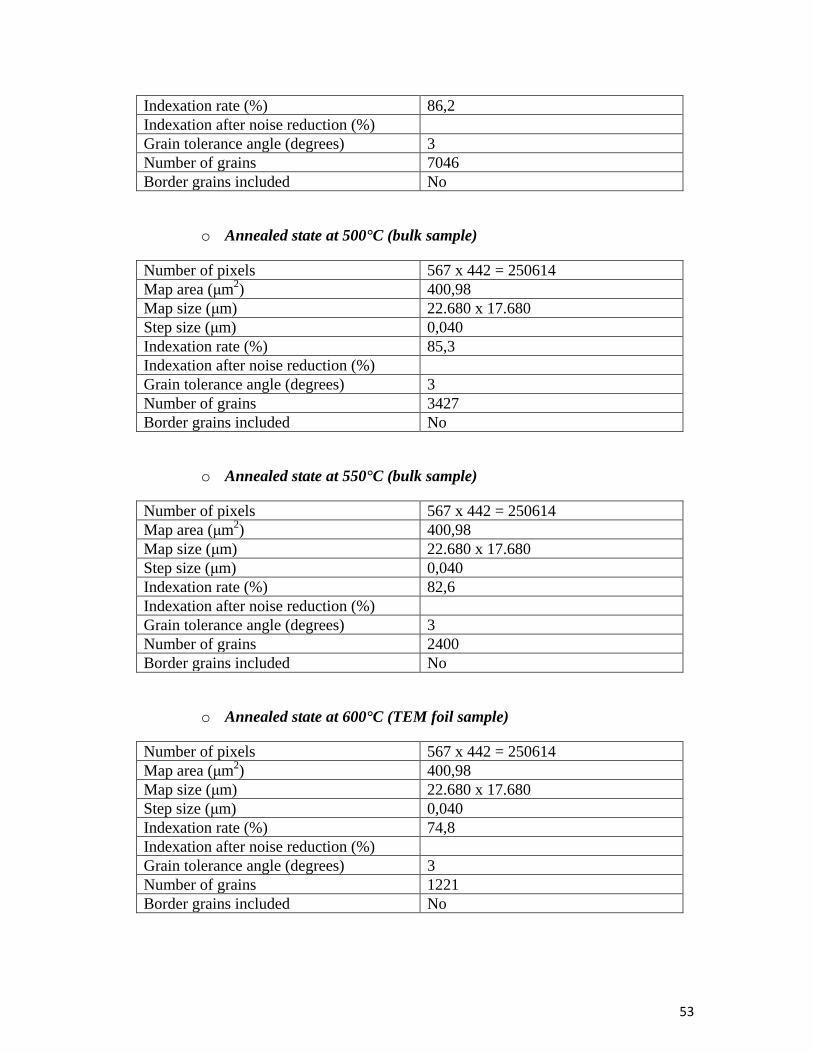
53
Indexation rate (%) 86,2
Indexation after noise reduction (%)
Grain tolerance angle (degrees) 3
Number of grains 7046
Border grains included No
o Annealed state at 500°C (bulk sample)
Number of pixels 567 x 442 = 250614
Map area (μm2) 400,98
Map size (μm) 22.680 x 17.680
Step size (μm) 0,040
Indexation rate (%) 85,3
Indexation after noise reduction (%)
Grain tolerance angle (degrees) 3
Number of grains 3427
Border grains included No
o Annealed state at 550°C (bulk sample)
Number of pixels 567 x 442 = 250614
Map area (μm2) 400,98
Map size (μm) 22.680 x 17.680
Step size (μm) 0,040
Indexation rate (%) 82,6
Indexation after noise reduction (%)
Grain tolerance angle (degrees) 3
Number of grains 2400
Border grains included No
o Annealed state at 600°C (TEM foil sample)
Number of pixels 567 x 442 = 250614
Map area (μm2) 400,98
Map size (μm) 22.680 x 17.680
Step size (μm) 0,040
Indexation rate (%) 74,8
Indexation after noise reduction (%)
Grain tolerance angle (degrees) 3
Number of grains 1221
Border grains included No