eem336 microprocessors i - ceng.eskisehir.edu.trceng.eskisehir.edu.tr/abilge/bim303/icerik/bim303 -...
TRANSCRIPT

EEM336 Microprocessors I
The Microprocessor and Its Architecture
EEM336 Microprocessors I 2The Microprocessor and Its Architecture
Introduction• This chapter presents the microprocessor as a
programmable device by first looking at its internal programming model and then how its memory space is addressed.
• The architecture of Intel microprocessors is presented, as are the ways that the family members address the memory system.
• Addressing modes for this powerful family of microprocessors are described for the real, protected, and flat modes of operation.

EEM336 Microprocessors I 3The Microprocessor and Its Architecture
Chapter Objectives
• Explain basic structure of Intel 8086 microprocessor, programming structure and software development flow
• Describe function and purpose of each program-visible register in the 8086-Core2 microprocessors, including 64-bit extensions.
• Detail the flag register and the purpose of each flag bit.
Upon completion of this chapter, you will be able to:

EEM336 Microprocessors I 4The Microprocessor and Its Architecture
Chapter Objectives
• Describe how memory is accessed using real mode memory-addressing techniques.
• Describe how memory is accessed using protected mode memory-addressing techniques.
• Describe how memory is accessed using the 64-bit flat memory model.
Upon completion of this chapter, you will be able to:(cont.)

EEM336 Microprocessors I 5The Microprocessor and Its Architecture
PROGRAMMING STRUCTURE• The lowest-level programming language is
the Machine language which is the only one understood by computers.
• While easily understood by computers, machine languages are almost impossible for humans to use because they consist entirely of numbers (e.g., 1s and 0s).

EEM336 Microprocessors I 6The Microprocessor and Its Architecture
PROGRAMMING STRUCTURE• Programmers, therefore, use either a high-
level programming language or an assembly language.
• An assembly language contains the same instructions as a machine language, but the instructions and variables have names instead of being just numbers.
EEM336 Microprocessors I 7The Microprocessor and Its Architecture
PROGRAMMING STRUCTURE• Every CPU has its own unique machine
language. Programs must be rewritten or recompiled to run on different types of computers.
• High-level languages are, however, platform independent. They can run on different types of computers.

EEM336 Microprocessors I 8The Microprocessor and Its Architecture
PROGRAMMING STRUCTURE

EEM336 Microprocessors I 9The Microprocessor and Its Architecture
SOFTWARE DEVELOPMENT FLOW

EEM336 Microprocessors I 10The Microprocessor and Its Architecture
SOFTWARE DEVELOPMENT FLOW• The following list describes sample tools that are
used for software development.• The compiler (e.g., C, C++, C#) translates source
code into assembly language source code.• The assembler translates assembly language
source files into machine language (object files). Source files contain numbers corresponding to instructions.

EEM336 Microprocessors I 11The Microprocessor and Its Architecture
SOFTWARE DEVELOPMENT FLOW• The linker combines object files created by the
assembler into a single executable object module. As it creates the executable module, it binds symbols to memory locations and resolves all references to those symbols. It also accepts library members and output modules created by a previous linker run.
• The cross-reference lister uses object files to produce a cross-reference listing showing variable and symbols, their definitions, memory locations and their references in the linked source files.

EEM336 Microprocessors I 12The Microprocessor and Its Architecture
Inside Intel 8086
• The 8086 is a 16-bit microprocessor chip designed by Intel in 1978, which gave rise to the x86 architecture.
• Intel 8088, released in 1979, was essentially the same chip, but with an external 8-bit data bus (allowing the use of cheaper and fewer supporting logic chips), and is notable as the processor used in the original IBM PC.

EEM336 Microprocessors I 13The Microprocessor and Its Architecture
Inside Intel 8086
8086 Pin Configuration

EEM336 Microprocessors I 14The Microprocessor and Its Architecture
Inside Intel 8086• All internal registers as well as internal and external
data buses of the 8086 are 16 bits wide, firmly establishing an actual "16-bit microprocessor".
• Clock rate of the first edition of 8086 was 5 MHz. Later, 8 and 10 MHz versions were also produced.
• A 20-bit external address bus gives a 1 MB (segmented) physical address space.
• 16-bit I/O addresses give 64 KB of separate I/O space.

EEM336 Microprocessors I 15The Microprocessor and Its Architecture
Inside Intel 8086• 8086 is internally divided
into two separate functional units.
1. Bus Interface Unit (BIU) 2. Execution Unit (EU).
• This concept of dividing work between two processors and processing it simultaneously (parallel processing) speeds up the execution.

EEM336 Microprocessors I 16The Microprocessor and Its Architecture
Inside Intel 8086
BUS INTERFACE UNIT
• The BIU sends out address, fetches instruction from memory, reads data from ports and memory and writes data to ports and memory. In other words the BIU handles all transfers of data and addresses on the buses for the execution unit.

EEM336 Microprocessors I 17The Microprocessor and Its Architecture
Inside Intel 8086INSTRUCTION QUEUE• To speed up the program execution BIU fetches as
many as 6 instruction bytes ahead of the memory. The pre fetch instruction bytes are held in Instruction Queue.The BIU can be fetching instruction bytes while EU is decoding or executing an instruction,which does not require the use of buses.
• When the EU is ready for its next instruction it simply reads the instruction from the queue in the BIU. This pre fetch and Queue scheme greatly speeds up processing. Fetching the next instruction while the current instruction executes is called Pipelining.

EEM336 Microprocessors I 18The Microprocessor and Its Architecture
Inside Intel 8086EXECUTION UNIT
• The EU of the 8086 tells the BIU, – where to fetch instructions or data from, – decodes instruction and executes instructions.
• The EU contains a 16 bit ALU which can add, subtract, AND, OR, XOR, increment, decrement, compliment or shift binary numbers.

EEM336 Microprocessors I 19The Microprocessor and Its Architecture
Inside Intel 8086

EEM336 Microprocessors I 20The Microprocessor and Its Architecture
INTERNAL MICROPROCESSOR ARCHITECTURE
• Before a program is written or instruction investigated, internal configuration of the microprocessor must be known.
• In a multiple core microprocessor each core contains the same programming model.
• Each core runs a separate task or thread simultaneously.

EEM336 Microprocessors I 21The Microprocessor and Its Architecture
The Programming Model• 8086 through Core2 considered program
visible.– particular registers are used during programming
and are specified by the instructions • Other registers considered to be program
invisible.– not addressable directly during applications
programming

EEM336 Microprocessors I 22The Microprocessor and Its Architecture
• 80286 and above contain program-invisible registers to control and operate protected memory. – and other features of the microprocessor
• 80386 through Core2 microprocessors contain full 32-bit internal architectures.
• 8086 through the 80286 are fully upward-compatible to the 80386 through Core2.
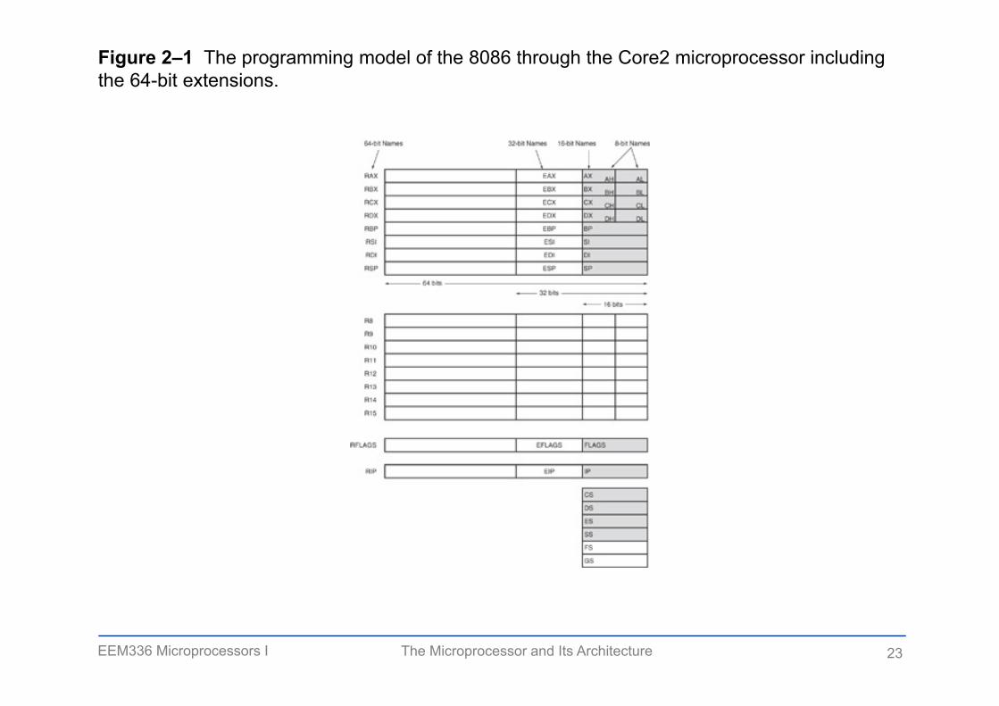
• Figure 2–1 illustrates the programming model 8086 through Core2 microprocessor.– including the 64-bit extensions
EEM336 Microprocessors I 23The Microprocessor and Its Architecture
Figure 2–1 The programming model of the 8086 through the Core2 microprocessor including the 64-bit extensions.
EEM336 Microprocessors I 24The Microprocessor and Its Architecture
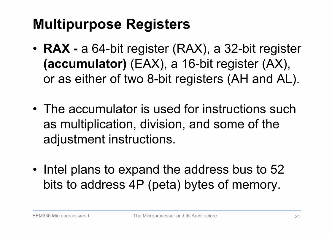
Multipurpose Registers• RAX - a 64-bit register (RAX), a 32-bit register
(accumulator) (EAX), a 16-bit register (AX), or as either of two 8-bit registers (AH and AL).
• The accumulator is used for instructions such as multiplication, division, and some of the adjustment instructions.
• Intel plans to expand the address bus to 52 bits to address 4P (peta) bytes of memory.

EEM336 Microprocessors I 25The Microprocessor and Its Architecture
• RBX, addressable as RBX, EBX, BX, BH, BL.– BX register (base index) sometimes holds offset
address of a location in the memory system in all versions of the microprocessor
• RCX, as RCX, ECX, CX, CH, or CL.– a (count) general-purpose register that also holds
the count for various instructions • RDX, as RDX, EDX, DX, DH, or DL.
– a (data) general-purpose register– holds a part of the result from a multiplication
or part of dividend before a division

EEM336 Microprocessors I 26The Microprocessor and Its Architecture
• RBP, as RBP, EBP, or BP.– points to a memory (base pointer) location
for memory data transfers• RDI addressable as RDI, EDI, or DI.
– often addresses (destination index) string destination data for the string instructions
• RSI used as RSI, ESI, or SI. – the (source index) register addresses source
string data for the string instructions– like RDI, RSI also functions as a general-
purpose register

EEM336 Microprocessors I 27The Microprocessor and Its Architecture
• R8 - R15 found in the Pentium 4 and Core2 if 64-bit extensions are enabled. – data are addressed as 64-, 32-, 16-, or 8-bit
sizes and are of general purpose• Most applications will not use these registers
until 64-bit processors are common. – the 8-bit portion is the rightmost 8-bit only– bits 8 to 15 are not directly addressable as
a byte

EEM336 Microprocessors I 28The Microprocessor and Its Architecture
Special-Purpose Registers• Include RIP, RSP, and RFLAGS
– segment registers include CS, DS, ES, SS, FS, and GS
• RIP addresses the next instruction in a section of memory.– defined as (instruction pointer) a code segment
• RSP addresses an area of memory called the stack. – the (stack pointer) stores data through this
pointer

EEM336 Microprocessors I 29The Microprocessor and Its Architecture
• RFLAGS indicate the condition of the microprocessor and control its operation.
• Figure 2–2 shows the flag registers of all versions of the microprocessor.
• Flags are upward-compatible from the 8086/8088 through Core2 .
• The rightmost five and the overflow flag are changed by most arithmetic and logic operations.– although data transfers do not affect them

EEM336 Microprocessors I 30The Microprocessor and Its Architecture
Figure 2–2 The EFLAG and FLAG register counts for the entire 8086 and Pentium microprocessor family.
• Flags never change for any data transfer or program control operation.
• Some of the flags are also used to control features found in the microprocessor.

EEM336 Microprocessors I 31The Microprocessor and Its Architecture
• Flag bits, with a brief description of function.• C (carry) holds the carry after addition or
borrow after subtraction. – also indicates error conditions
• P (parity) is the count of ones in a number expressed as even or odd. Logic 0 for odd parity; logic 1 for even parity. – if a number contains three binary one bits, it has
odd parity– if a number contains no one bits, it has even
parity

EEM336 Microprocessors I 32The Microprocessor and Its Architecture
List of Each Flag bit, with a brief description of function.
• C (carry) holds the carry after addition or borrow after subtraction. – also indicates error conditions
• P (parity) is the count of ones in a number expressed as even or odd. Logic 0 for odd parity; logic 1 for even parity. – if a number contains three binary one bits, it has
odd parity; If a number contains no one bits, ithas even parity

EEM336 Microprocessors I 33The Microprocessor and Its Architecture
• A (auxiliary carry) holds the carry (half-carry) after addition or the borrow after subtraction between bit positions 3 and 4 of the result.
• Z (zero) shows that the result of an arithmetic or logic operation is zero.
• S (sign) flag holds the arithmetic sign of the result after an arithmetic or logic instruction executes.
• T (trap) The trap flag enables trapping through an on-chip debugging feature.
EEM336 Microprocessors I 34The Microprocessor and Its Architecture
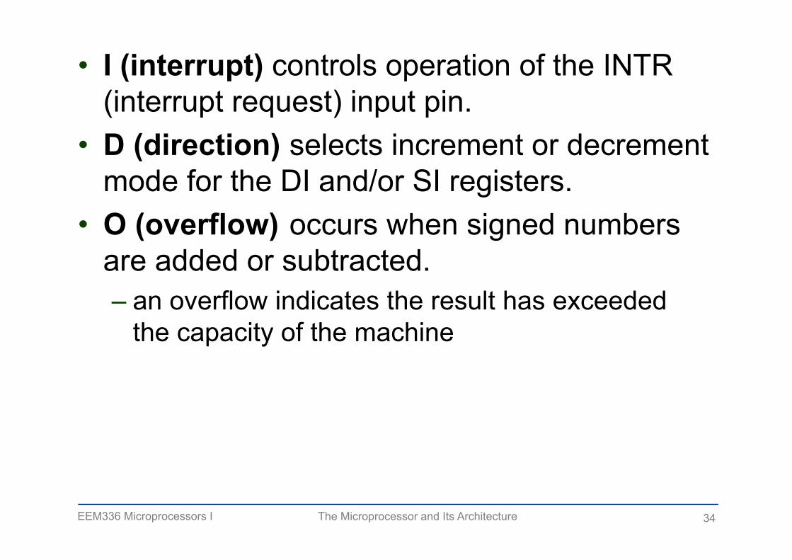
• I (interrupt) controls operation of the INTR (interrupt request) input pin.
• D (direction) selects increment or decrement mode for the DI and/or SI registers.
• O (overflow) occurs when signed numbers are added or subtracted. – an overflow indicates the result has exceeded
the capacity of the machine

EEM336 Microprocessors I 35The Microprocessor and Its Architecture
• IOPL used in protected mode operationto select the privilege level for I/O devices.
• NT (nested task) flag indicates the current task is nested within another task in protected mode operation.
• RF (resume) used with debugging to control resumption of execution after the next instruction.
• VM (virtual mode) flag bit selects virtual mode operation in a protected mode system.

EEM336 Microprocessors I 36The Microprocessor and Its Architecture
• AC, (alignment check) flag bit activates if a word or doubleword is addressed on a non-word or non-doubleword boundary.
• VIF is a copy of the interrupt flag bit available to the Pentium 4–(virtual interrupt)
• VIP (virtual) provides information about a virtual mode interrupt for (interrupt pending)Pentium. – used in multitasking environments to provide
virtual interrupt flags

EEM336 Microprocessors I 37The Microprocessor and Its Architecture
• ID (identification) flag indicates that the Pentium microprocessors support the CPUID instruction. – CPUID instruction provides the system with
information about the Pentium microprocessor

EEM336 Microprocessors I 38The Microprocessor and Its Architecture
Segment Registers• Generate memory addresses when combined
with other registers in the microprocessor.• Four or six segment registers in various
versions of the microprocessor.• A segment register functions differently in real
mode than in protected mode.• Following is a list of each segment register,
along with its function in the system.

EEM336 Microprocessors I 39The Microprocessor and Its Architecture
• CS (code) segment holds code (programs and procedures) used by the microprocessor.
• DS (data) contains most data used by a program. – Data are accessed by an offset address or
contents of other registers that hold the offset address
• ES (extra) an additional data segment used by some instructions to hold destination data.
EEM336 Microprocessors I 40The Microprocessor and Its Architecture
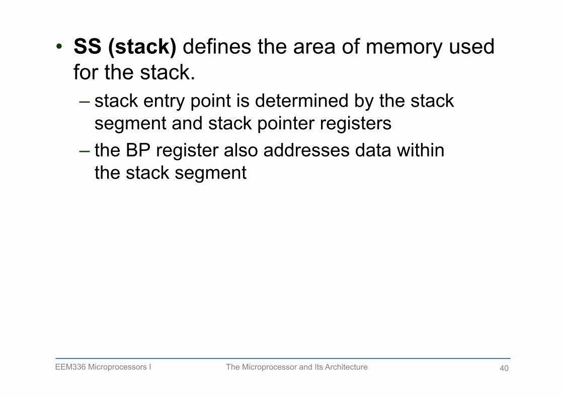
• SS (stack) defines the area of memory used for the stack. – stack entry point is determined by the stack
segment and stack pointer registers – the BP register also addresses data within
the stack segment

EEM336 Microprocessors I 41The Microprocessor and Its Architecture
• FS and GS segments are supplemental segment registers available in 80386–Core2 microprocessors.– allow two additional memory segments for
access by programs • Windows uses these segments for internal
operations, but no definition of their usageis available.

EEM336 Microprocessors I 42The Microprocessor and Its Architecture
REAL MODE MEMORY ADDRESSING
• 80286 and above operate in either the real or protected mode.
• Real mode operation allows addressing of only the first 1M byte of memory space—even in Pentium 4 or Core2 microprocessor. – the first 1M byte of memory is called the real
memory, conventional memory, or DOS memory system

EEM336 Microprocessors I 43The Microprocessor and Its Architecture
Segments and Offsets• All real mode memory addresses must consist
of a segment address plus an offset address. – segment address defines the beginning address
of any 64K-byte memory segment– offset address selects any location within the
64K byte memory segment• Figure 2–3 shows how the segment plus
offset addressing scheme selects a memory location.

EEM336 Microprocessors I 44The Microprocessor and Its Architecture
Figure 2–3 The real mode memory-addressing scheme, using a segment address plus an offset.
– this shows a memory segment beginning at 10000H, ending at location IFFFFH
• 64K bytes in length
– also shows how an offset address, called a displacement, of F000H selects location1F000H in the memory

EEM336 Microprocessors I 45The Microprocessor and Its Architecture
• Once the beginning address is known, the ending address is found by adding FFFFH.– because a real mode segment of memory is 64K
in length• The offset address is always added to the
segment starting address to locate the data.• Segment and offset address is sometimes
written as 1000:2000.– a segment address of 1000H; an offset of 2000H

EEM336 Microprocessors I 46The Microprocessor and Its Architecture
Default Segment and Offset Registers
• The microprocessor has rules that apply to segments whenever memory is addressed. – these define the segment and offset register
combination • The code segment register defines the start
of the code segment.• The instruction pointer locates the next
instruction within the code segment.

EEM336 Microprocessors I 47The Microprocessor and Its Architecture
• Another of the default combinations is the stack. – stack data are referenced through the stack
segment at the memory location addressed by either the stack pointer (SP/ESP) or the pointer (BP/EBP)
• Figure 2–4 shows a system that contains four memory segments.– a memory segment can touch or overlap if 64K
bytes of memory are not required for a segment

EEM336 Microprocessors I 48The Microprocessor and Its Architecture
Figure 2–4 A memory system showing the placement of four memory segments.
– think of segments as windows that can be moved over any areaof memory to access data or code
– a program can have more than four or six segments,
• but only access four or six segments at a time

EEM336 Microprocessors I 49The Microprocessor and Its Architecture
Figure 2–5 An application program containing a code, data, and stack segment loaded into a DOS system memory.
– a program placed in memory by DOS is loaded in the TPA at the first available area of memory above drivers and other TPA programs
– area is indicated by a free-pointer maintained by DOS
– program loading is handled automatically by the program loader within DOS

EEM336 Microprocessors I 50The Microprocessor and Its Architecture
Segment and Offset Addressing Scheme Allows Relocation
• Segment plus offset addressing allows DOS programs to be relocated in memory.
• A relocatable program is one that can be placed into any area of memory and executed without change.
• Relocatable data are data that can be placed in any area of memory and used without any change to the program.

EEM336 Microprocessors I 51The Microprocessor and Its Architecture
• Because memory is addressed within a segment by an offset address, the memory segment can be moved to any place in the memory system without changing any of the offset addresses.
• Only the contents of the segment register must be changed to address the programin the new area of memory.
• Windows programs are written assuming that the first 2G of memory are available for code and data.

EEM336 Microprocessors I 52The Microprocessor and Its Architecture
INTRO TO PROTECTED MODEMEMORY ADDRESSING
• Allows access to data and programs located within & above the first 1M byte of memory.
• Protected mode is where Windows operates.• In place of a segment address, the segment
register contains a selector that selects a descriptor from a descriptor table.
• The descriptor describes the memory segment’s location, length, and access rights.

EEM336 Microprocessors I 53The Microprocessor and Its Architecture
Selectors and Descriptors• The descriptor is located in the segment
register & describes the location, length, and access rights of the segment of memory. – it selects one of 8192 descriptors from one
of two tables of descriptors• In protected mode, this segment number can
address any memory location in the systemfor the code segment.
• Indirectly, the register still selects a memory segment, but not directly as in real mode.

EEM336 Microprocessors I 54The Microprocessor and Its Architecture
Flat Mode Memory• A flat mode memory system is one in which
there is no segmentation. – does not use a segment register to address a
location in the memory• First byte address is at 00 0000 0000H; the
last location is at FF FFFF FFFFH. – address is 40-bits
• The segment register still selects the privilege level of the software.

EEM336 Microprocessors I 55The Microprocessor and Its Architecture
• Real mode system is not available if the processor operates in the 64-bit mode.
• Protection and paging are allowed in the 64-bit mode.
• The CS register is still used in the protected mode operation in the 64-bit mode.
• Most programs today are operated in the IA32 compatible mode.– current software operates properly, but this will
change in a few years as memory becomeslarger and most people have 64-bit computers

EEM336 Microprocessors I 56The Microprocessor and Its Architecture
Figure 2–15 The 64-bit flat mode memory model.

EEM336 Microprocessors I 57The Microprocessor and Its Architecture
The Intel Microprocessors: 8086/8088, 80186/80188, 80286, 80386, 80486 Pentium, Pentium Pro Processor, Pentium II, Pentium, 4, and Core2 with 64-bit Extensions Architecture, Programming, and Interfacing, Eighth EditionBarry B. Brey
Copyright ©2009 by Pearson Education, Inc.Upper Saddle River, New Jersey 07458 • All rights reserved.