eem328 electronics laboratory - experiment 7 - jfet amplifiers
DESCRIPTION
This experiment will investigate the characteristics of the common-source and common-drain amplifiers.TRANSCRIPT

EEM 328 ELECTRONICS LABORATORY
EXPERIMENT 7 JFET AMPLIFIERS
PURPOSE This experiment will investigate the characteristics of the common-source and common-drain amplifiers. THEORY In this lab, two JFET amplifier configurations will be investigated; the common source, and the common-drain amplifier. The basic common-source (CS) circuit is shown in Figure 1. In comparison to the BJT common-emitter amplifier, the FET amplifier has much higher input impedance, but a lower voltage gain. The voltage gain of the circuit can be expressed as
Av ≈ - gmRD
Figure 1 Common source amplifier
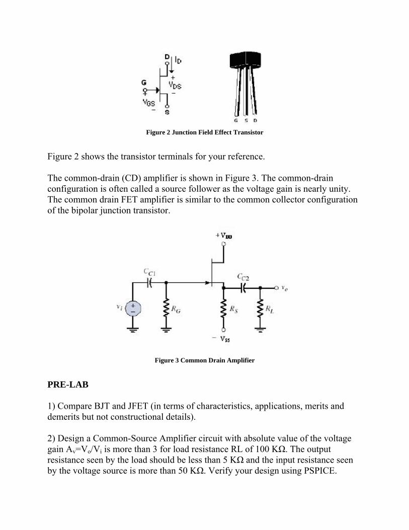
Figure 2 Junction Field Effect Transistor
Figure 2 shows the transistor terminals for your reference. The common-drain (CD) amplifier is shown in Figure 3. The common-drain configuration is often called a source follower as the voltage gain is nearly unity. The common drain FET amplifier is similar to the common collector configuration of the bipolar junction transistor.
Figure 3 Common Drain Amplifier
PRE-LAB 1) Compare BJT and JFET (in terms of characteristics, applications, merits and demerits but not constructional details). 2) Design a Common-Source Amplifier circuit with absolute value of the voltage gain Av=Vo/Vi is more than 3 for load resistance RL of 100 KΩ. The output resistance seen by the load should be less than 5 KΩ and the input resistance seen by the voltage source is more than 50 KΩ. Verify your design using PSPICE.
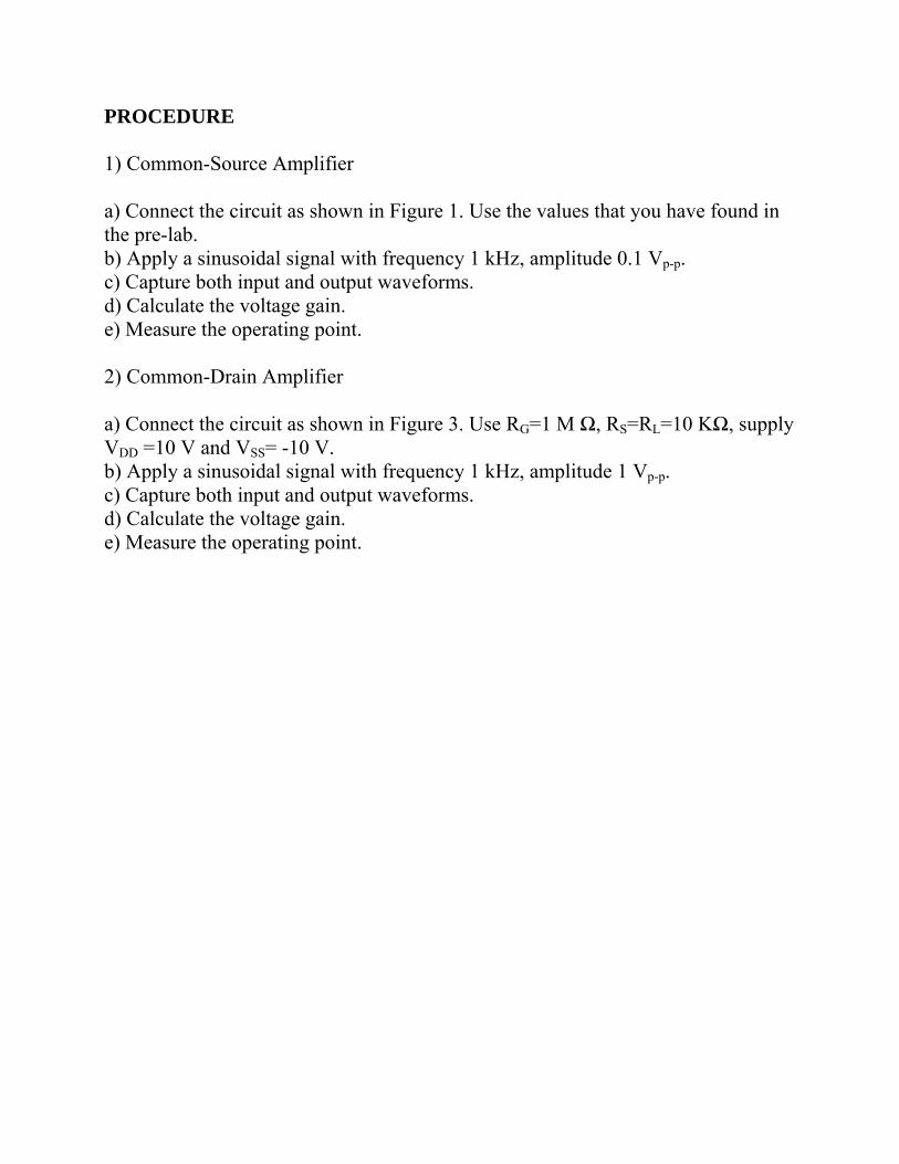
PROCEDURE 1) Common-Source Amplifier a) Connect the circuit as shown in Figure 1. Use the values that you have found in the pre-lab. b) Apply a sinusoidal signal with frequency 1 kHz, amplitude 0.1 Vp-p. c) Capture both input and output waveforms. d) Calculate the voltage gain. e) Measure the operating point. 2) Common-Drain Amplifier a) Connect the circuit as shown in Figure 3. Use RG=1 M Ω, RS=RL=10 KΩ, supply VDD =10 V and VSS= -10 V. b) Apply a sinusoidal signal with frequency 1 kHz, amplitude 1 Vp-p. c) Capture both input and output waveforms. d) Calculate the voltage gain. e) Measure the operating point.