eem328 electronics laboratory - experiment 5 - bjt amplifiers
DESCRIPTION
In this experiment, amplifiers with a BJT will be studied and an amplifier circuit will be designed and tested.TRANSCRIPT
ELECTRONICS LABORATORY EXPERIMENT 5
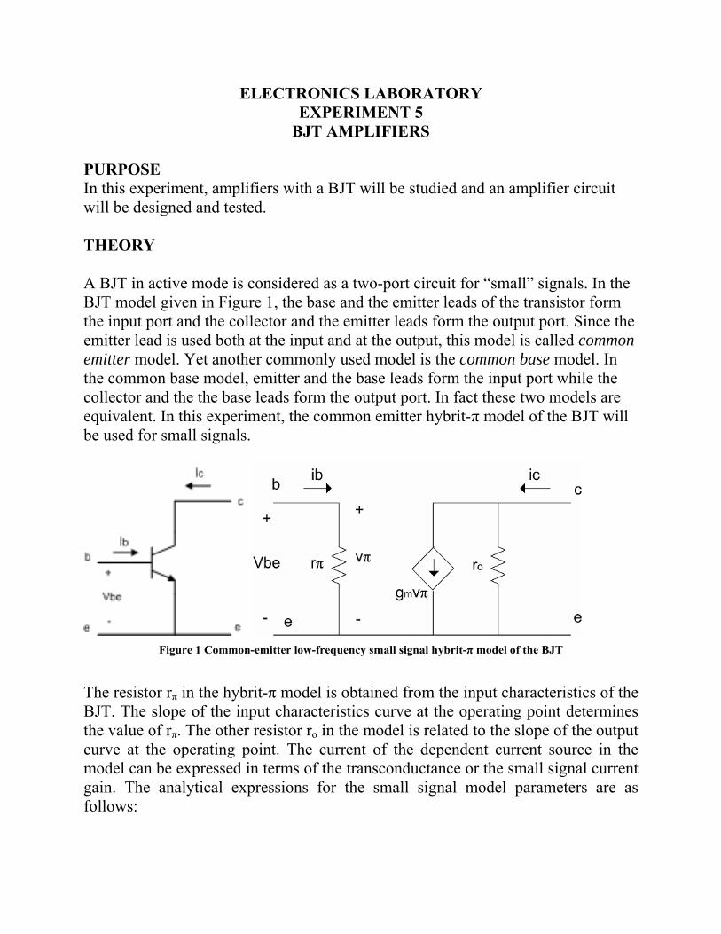
BJT AMPLIFIERS PURPOSE In this experiment, amplifiers with a BJT will be studied and an amplifier circuit will be designed and tested. THEORY A BJT in active mode is considered as a two-port circuit for “small” signals. In the BJT model given in Figure 1, the base and the emitter leads of the transistor form the input port and the collector and the emitter leads form the output port. Since the emitter lead is used both at the input and at the output, this model is called common emitter model. Yet another commonly used model is the common base model. In the common base model, emitter and the base leads form the input port while the collector and the the base leads form the output port. In fact these two models are equivalent. In this experiment, the common emitter hybrit-π model of the BJT will be used for small signals.
Figure 1 Common-emitter low-frequency small signal hybrit-π model of the BJT
The resistor rπ in the hybrit-π model is obtained from the input characteristics of the BJT. The slope of the input characteristics curve at the operating point determines the value of rπ. The other resistor ro in the model is related to the slope of the output curve at the operating point. The current of the dependent current source in the model can be expressed in terms of the transconductance or the small signal current gain. The analytical expressions for the small signal model parameters are as follows:
TVIQ
dvdig cc
mBE
== (1)
m
o
gQ
didvr
B
BE βπ == (2)
cIA
c
VQdidvr CE
o == (3)
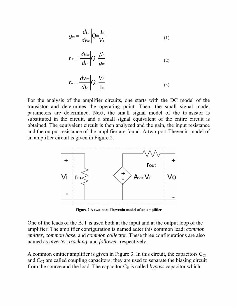
For the analysis of the amplifier circuits, one starts with the DC model of the transistor and determines the operating point. Then, the small signal model parameters are determined. Next, the small signal model of the transistor is substituted in the circuit, and a small signal equivalent of the entire circuit is obtained. The equivalent circuit is then analyzed and the gain, the input resistance and the output resistance of the amplifier are found. A two-port Thevenin model of an amplifier circuit is given in Figure 2.
Figure 2 A two-port Thevenin model of an amplifier
One of the leads of the BJT is used both at the input and at the output loop of the amplifier. The amplifier configuration is named adter this common lead: common emitter, common base, and common collector. These three configurations are also named as inverter, tracking, and follower, respectively. A common emitter amplifier is given in Figure 3. In this circuit, the capacitors CC1 and CC2 are called coupling capacitors; they are used to separate the biasing circuit from the source and the load. The capacitor CE is called bypass capacitor which
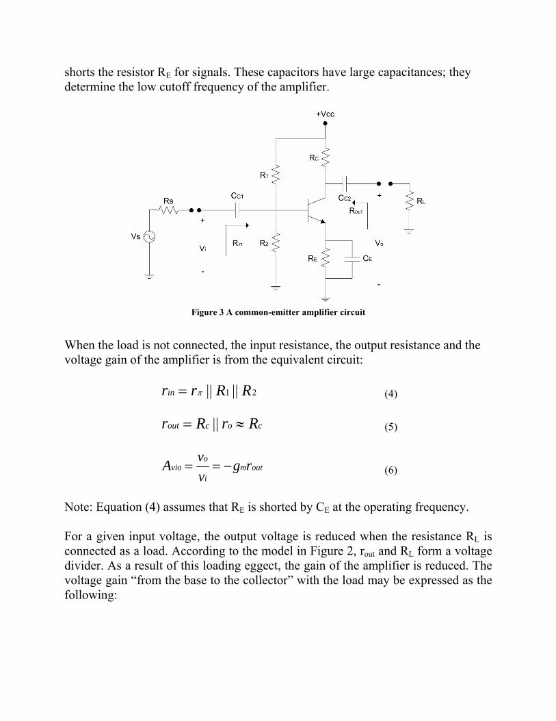
shorts the resistor RE for signals. These capacitors have large capacitances; they determine the low cutoff frequency of the amplifier.
Figure 3 A common-emitter amplifier circuit
When the load is not connected, the input resistance, the output resistance and the voltage gain of the amplifier is from the equivalent circuit:
21 |||| RRrrin π= (4)
cocout RrRr ≈= || (5)
outmi
ovio rg
vvA −== (6)
Note: Equation (4) assumes that RE is shorted by CE at the operating frequency. For a given input voltage, the output voltage is reduced when the resistance RL is connected as a load. According to the model in Figure 2, rout and RL form a voltage divider. As a result of this loading eggect, the gain of the amplifier is reduced. The voltage gain “from the base to the collector” with the load may be expressed as the following:
⎟⎠⎞⎜
⎝⎛−== Loutm
i
ovi Rrg
vvA || (7)
Similar to the loading effect at the output, the amplifier circuit loads the signal source. The output resistance of the source and the input resistance of the amplifier form a voltage divider. Hence, the voltage at the base of the BJT becomes
ins
insi
rrrvv+
= (8)
and the voltage gain “from the source to the load” is now
ins
inLoutm
s
ovs
rrrRrg
vvA
+−== ⎟
⎠⎞⎜
⎝⎛ || (9)
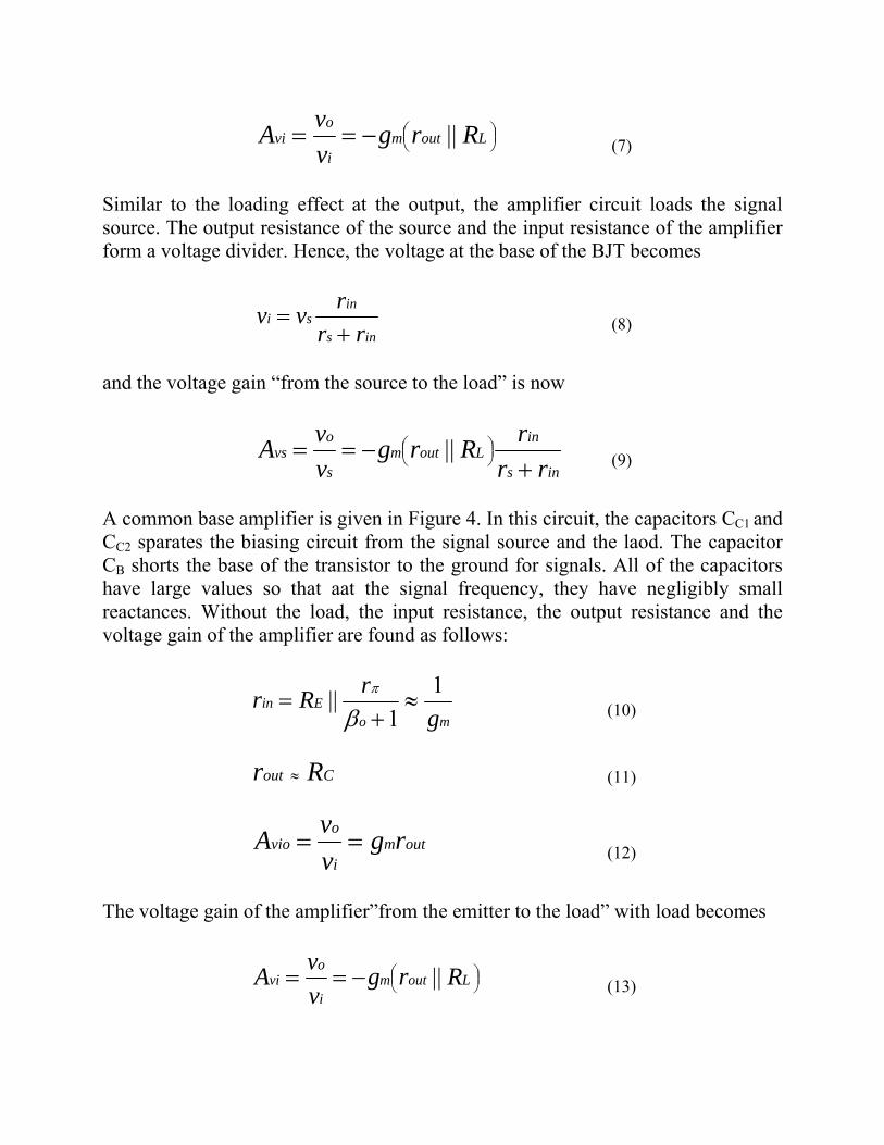
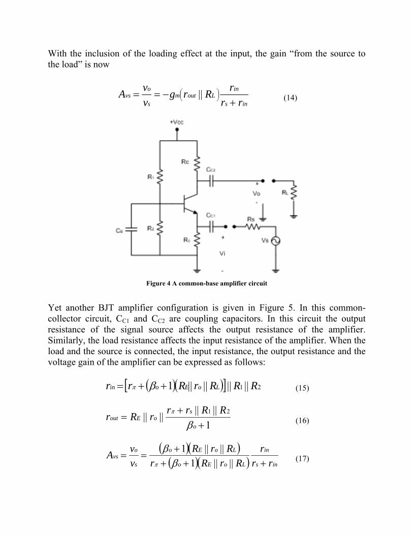
A common base amplifier is given in Figure 4. In this circuit, the capacitors CC1 and CC2 sparates the biasing circuit from the signal source and the laod. The capacitor CB shorts the base of the transistor to the ground for signals. All of the capacitors have large values so that aat the signal frequency, they have negligibly small reactances. Without the load, the input resistance, the output resistance and the voltage gain of the amplifier are found as follows:
moEin
grRr 1
1|| ≈
+=
βπ
(10)
Cout Rr ≈ (11)
outmi
ovio rg
vvA == (12)
The voltage gain of the amplifier”from the emitter to the load” with load becomes
⎟⎠⎞⎜
⎝⎛−== Loutm
i
ovi Rrg
vvA || (13)
With the inclusion of the loading effect at the input, the gain “from the source to the load” is now
ins
inLoutm
s
ovs
rrrRrg
vvA
+−== ⎟
⎠⎞⎜
⎝⎛ || (14)
Figure 4 A common-base amplifier circuit
Yet another BJT amplifier configuration is given in Figure 5. In this common-collector circuit, CC1 and CC2 are coupling capacitors. In this circuit the output resistance of the signal source affects the output resistance of the amplifier. Similarly, the load resistance affects the input resistance of the amplifier. When the load and the source is connected, the input resistance, the output resistance and the voltage gain of the amplifier can be expressed as follows:
( )( )[ ] 21 ||||||||1 RRRrRrr LoEoin ++= βπ (15)
1|||||||| 21
++
=o
soEout
RRrrrRrβ
π (16)
( )( )( )( ) ins
in
LoEo
LoEo
s
ovs
rrr
RrRrRrR
vvA
++++
==||||1
||||1β
βπ
(17)
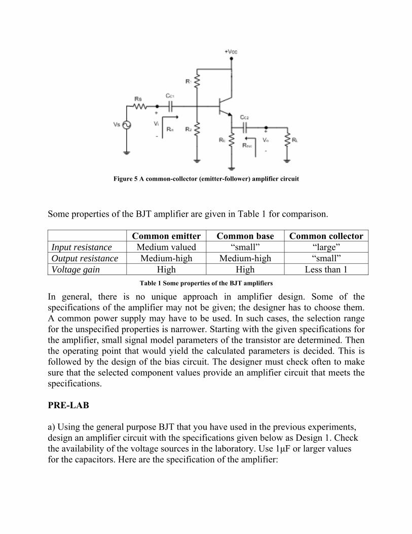
Figure 5 A common-collector (emitter-follower) amplifier circuit
Some properties of the BJT amplifier are given in Table 1 for comparison. Common emitter Common base Common collector Input resistance Medium valued “small” “large” Output resistance Medium-high Medium-high “small” Voltage gain High High Less than 1
Table 1 Some properties of the BJT amplifiers
In general, there is no unique approach in amplifier design. Some of the specifications of the amplifier may not be given; the designer has to choose them. A common power supply may have to be used. In such cases, the selection range for the unspecified properties is narrower. Starting with the given specifications for the amplifier, small signal model parameters of the transistor are determined. Then the operating point that would yield the calculated parameters is decided. This is followed by the design of the bias circuit. The designer must check often to make sure that the selected component values provide an amplifier circuit that meets the specifications. PRE-LAB a) Using the general purpose BJT that you have used in the previous experiments, design an amplifier circuit with the specifications given below as Design 1. Check the availability of the voltage sources in the laboratory. Use 1µF or larger values for the capacitors. Here are the specification of the amplifier:

“the remainder” Design 1 Design 2 Design 3 Load 10 kΩ 10 kΩ 150 Ω Input resistance > 1 kΩ 75-100 Ω > 20 kΩ Output resistance < 10 kΩ < 10 kΩ 100-150 Ω Voltage gain > 40 > 50 Close to 1
b) Analyze the circuit with PSPICE or WORKBENCH simulation programs. You can give an AC signal source with a magnitude of 1 mV. Analyze how the gain changes with frequency. Obtain the voltage gain with and without the load. Are they different? Determine the output resistance. PROCEDURE 1) Set up the circuit designed in the preliminary work and measure its gain with a 1 kHz sine signal. 2) Connect a resistor – with a value close to the input of the amplifier – between the signal source and the input of the amplifier in series. Measure the signal voltage at both ends of this resistor, and calcultate the input current and the input resistance of the amplifier. 3) Determine the output resistance of the amplifier by measuring the output voltage with and without the load. 4) Compare your design values, PSPICE analysis results and the experimental results. Explain possible sources of disagreements if there are any.