eee225 transistor ampli er circuit analysis problem sheet · ravazi has also written some very well...
TRANSCRIPT

EEE225 Transistor Amplifier CircuitAnalysis Problem Sheet
This problem sheet builds on the analysis of the two transistor amplifier cir-cuits EEE118. It should prepare students well to tackle general problems in-volving transistors in analogue circuits. The circuits used in questions 1, 2 & 3are not directly examinable, nor are questions 8 – 10. The techniques needed tosolve the first few questions are the standard techniques of circuit analysis withactive devices. These techniques were first introduced in EEE118 and are furtherdeveloped in EEE225. If you can solve questions 1 – 3 confidently you’ll have noproblem at all with questions 4 – 7 which are examinable. Question 7 is quitesimilar to the sort of questions that come up in EEE223, and some parts of it todo with crossover distortion are in EEE225 as well.
How to tackle this sheetDo question 1 or question 2 or question 3. Do all of questions 4, 5 & 6. Someof question 7 is needed in EEE225 especially related to crossover distortion, therest is needed in EEE223.
If you feel that you’ve not had enough practice, go back and do the otherquestions as well. It would certainly be a good idea to look at the past exampapers as well for practice questions. You should find the exam questions mucheasier than the problems in this sheet, consiquently if you can do the sheet theexam should not pose any difficulty.
Questions 8 – 10 are for students who love the topic and want to go onan adventure of their own. The solution of these questions uses many of thetechniques in this course but also moves outside the scope of the course. Unlessyou have lots of time available having done all the other quesetions and being upto date with all your other modules I would not devote time to these questions.
If you’re looking for even more analogue try Gray, Hurst, Lewis and Meyer,which is considered by many to be the standard text on the subject. BehzadRavazi has also written some very well liked books on the topic. He also hasvideo lectures on YouTube which covers much of EEE118 and the semicon-ductors and analogue aspects of EEE225 https://www.youtube.com/watch?v=
yQDfVJzEymI&list=PL7qUW0KPfsIIOPOKL84wK_Qj9N7gvJX6v
Question 1: A Common Emitter CircuitThis question is about the “type 1” common emitter circuit from EEE118. Unlessotherwise stated, assume that all capacitors are short circuit in the mid-band.Some solutions will be easier to reach if RL and RC are lumped together as R′L.Similarly RB may be used to represent the parallel combination of R1 and R2.
1
The objective with the small signal derivations is to show which componentsare in control of certain circuit parameters, therefore the final form of the answershould be manipulated to reveal this information as clearly as possible. Arrangingequations in a way that reveals certain underlying relationships in the circuitparameters is something computers are not very good at, this sort of work is bestdone by hand.
1. Find the DC conditions of the common emitter circuit in Figure 1 assumingthe base current of Q1 can be ignored.
2. Find the DC conditions again but taking into consideration the base current.Perform your calculations for the full range of hFE. Find the range of hFEfrom the Fairchild Semiconductor BC549 datasheet.
3. Explain (briefly, using bullet points for example) the job of each componentin the circuit.
4. Explain (in words) why the emitter resistor, RE acts to reduce the gain ofthe circuit unless it is decoupled by CE.
5. Draw and label the small signal equivalent circuit for Figure 1.
6. Calculate the small signal transconductance, gm, and base emitter resis-tance, rbe for the range of hFE given in the Fairchild Semiconductor datasheet.You may assume that the transistor stage will be operated at frequenciesconsiderably below the transition frequency, fT , and therefore β = hFE
7. Show that the mid-band voltage gain of the common emitter circuit shownin Figure 1 is given by (1).
8. Show that the mid-band output resistance of the amplifier circuit in Figure 1is given by (2).
9. Show that the mid-band input resistance of the amplifier circuit in Figure 1is given by (3).
10. Show that the mid-band current gain given by (4).
11. Find an expression for the transresistance vo/ii of the amplifier stage shownin Figure 1.
12. Draw and label the small signal equivalent circuit for Figure 1 if CE is opencircuit at all frequencies of interest, all other capacitors may be consideredshort circuit.
2

13. Assuming CE is open circuit at all frequencies of interest, derive the inputresistance, output resistance, voltage gain and current gain of the amplifier.The final solutions take the forms shown in (5) - (8).
14. Given your solution for the small signal properties of the stage withoutemitter decoupling, determine what components are in control of the voltagegain, current gain, input resistance and output resistance. Comment on theeffect of emitter degeneration on the small signal parameters. For example,which components are in control of the voltage gain? Which componentsdominate input resistance? What are the main components which reducecurrent gain?
15. State the numerical values of voltage gain, current gain, power gain, inputresistance and output resistance with and without emitter decoupling overthe range of hFE given in the datasheet.
Figure 1: A common emitter amplifier circuit.
vovi
= − gmR′L
Rs(
1RB
+ gmβ
)+ 1
(1)
ro =voit
= RC (2)
ri =viii
=1
1RB
+ gmβ
(3)
3

ioii
= βRB
RB + rbeor
β
1 + βgmRB
(4)
vovi
= − gmR′L
RS
(1RB
+ gmβ
+ 1RS
+ (β+1)β
RE gm
(1RB
+ 1RS
)) (5)
ri =1 + β
gmRE (β+1)
1RB
+ 1RE (β+1)
+ βgmRE RB (β+1)
(6)
ro = RC (7)
ioii
= − β
β(
1gmRB
+ RE
RB
)+ RE
RB+ 1
(8)
Question 2: A Common Base CircuitThis question is about a capacitively coupled common base amplifier.
1. Find the DC conditions of the common base circuit in Figure 2 assumingthe base current of Q1 can be ignored.
2. Find the DC conditions again but taking into consideration the base current.Perform your calculations for the full range of hFE. Find the range of hFEfrom the On Semiconductor MJE340 datasheet.
3. Explain (briefly, using bullet points for example) the job of each componentin the circuit.
4. Draw and label the small signal equivalent circuit for Figure 2.
5. Calculate the small signal transconductance, gm, and base emitter resis-tance, rbe for the range of hFE given in the Fairchild Semiconductor datasheet.You may assume that the transistor stage will be operated at low frequen-cies and therefore β = hFE
6. Assuming the capacitors are short circuit at all frequencies of interest, showthat the input resistance of the amplifier circuit in Figure 2 is given by (9).
7. Assuming the capacitors are short circuit at all frequencies of interest, showthat the output resistance of the amplifier circuit in Figure 2 is RC .
8. Assuming the capacitors are short circuit at all frequencies of interest, showthat the transresistance (output voltage / input current) gain of the com-mon base circuit shown in Figure 2 is given by (11).
4

9. Derive an expression for the current gain. Solution: (12).
10. Derive an expression for the voltage gain. Solution: (13).
11. Practical transistors have a physical resistance between the active part ofthe base region and the transistor package leg. This is partly made from theohmic bond-wire resistance inside the package and partly made from theohmic resistance of the semiconductor between the position at which thebond wire is attached to the semiconducor and the position of the activepart of the base material. Draw the small signal equivalent circuit assumingthat this base spreading resistance, rb, appears in series with the base leg.C1 is still short circuit at all frequencies of interest.
12. Re-derive your small signal results so far assuming taking into account thebase spreading resistance. The results are shown in (14) - (17).
13. Reflect on and then qualitatively describe (i.e. in words) the effect of thebase spreading resistance on the stage’s small signal parameters. Commenton the similarity of the feedback provided by lifting the base node in thecommon base circuit with the effects of degenerating the emitter in thecommon emitter circuit.
14. State the numerical values of the small signal metrics of performance withand without the base spreading resistance over the range of β. You mayassume that the amplifier is operated at a low frequency and thereforeβ = hFE
veiin
=1
gmβ
+ gm + 1RE
(9)
voio
= RC (10)
voiin
=gmR
′L
gmβ
+ gm + 1R′
E
(11)
βrbe
1rbe
+ βrbe
+ 1R′
E
≈ α (12)
vovi
=gmR
′L(
1rbe
+ gm + 1Rs
+ 1RE
) (13)
veiin≈ rbβ
+1
gm(14)
5

voiin
=R′L
1+ββ
+ 1gmR′
E+ rb
R′E β
(15)
ioiin
=1
1+ββ
+ 1gmR′
E+ rb
R′E β
(16)
vovin
=gmR
′L
Rs
(gmβ
+ 1Rs
+ gm rbβ Rs
+ gm + 1RE
+ gm rbβ RE
) (17)
Figure 2: Common Base Amplifier Circuit
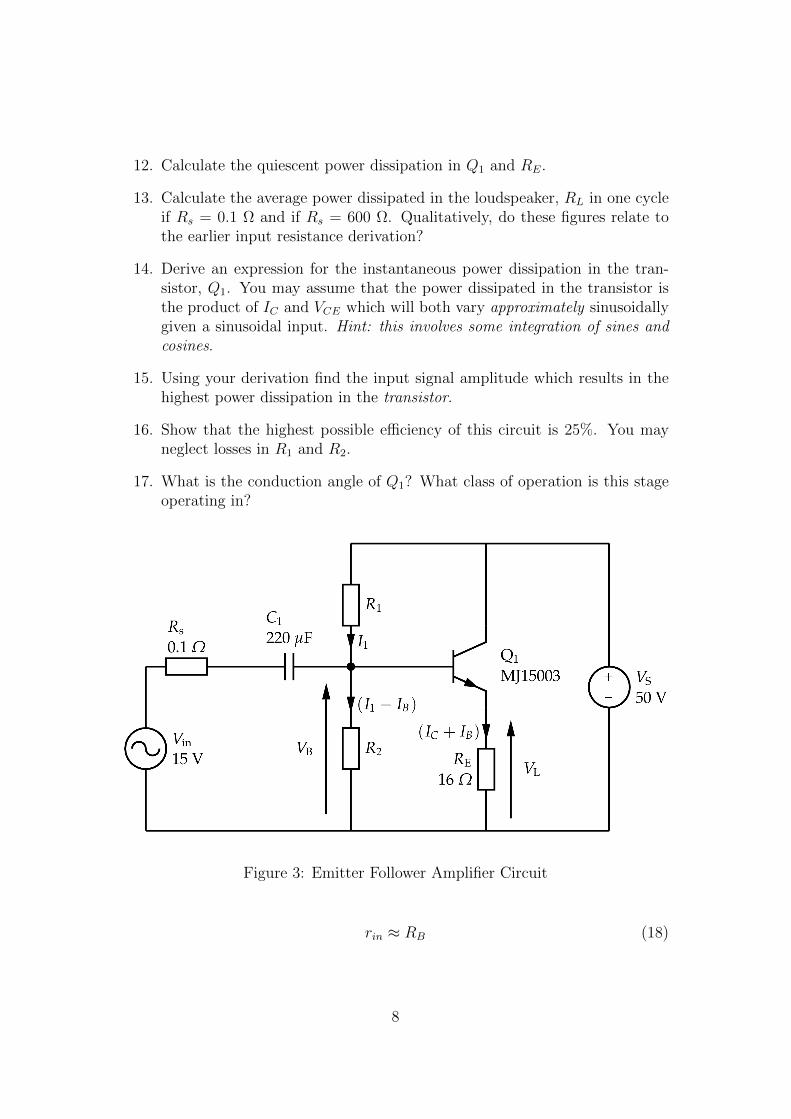
Question 3: An Emitter Follower CircuitThis question is about a capacitively coupled emitter (common collector) followeramplifier, shown in Figure 3. This emitter follower stage is used to drive a 16 Ωloudspeaker represented by RE. The DC current biasing the stage also flowsthrough RE. This is often not practical but for the sake of making the questioneasier we will assume that this is a magical speaker (from my office...) that doesn’tmind having a large DC component of current flowing through it. Of course theDC current dissipates power in the speaker but this would not be useful outputpower (sound) it would be heat. It would also hold the voice coil away from thecenter position but as we have said all these problems are ignored for the sake ofsimplicity.
1. Find the DC conditions of the emitter follower circuit in Figure 3 assumingthe base current of Q1 can be ignored. Choose VB such that VL, the emitter
6
voltage, is half way between the power supply and ground, thereby providingthe largest possible output voltage swing.
2. Find the DC conditions again but taking into consideration the base current.Perform your calculations for the full range of hFE. Find the range of hFEfrom the On Semiconductor MJ15003 datasheet.
3. Explain (briefly, using bullet points for example) the purpose of each com-ponent in the circuit.
4. Sketch the output characteristic (VCE vs IC as a function of VBE or IB), addthe operating point and the load line. On secondary axes, sketch the timedependent sinusoidal waveforms showing how the operating point movesaccording to the input signal, Vin and the output signal, VL that resultsfrom this input.
5. Draw and label the small signal equivalent circuit for Figure 3.
6. Calculate the small signal transconductance, gm, and base emitter resis-tance, rbe at the operating point for the range of hFE given in the OnSemiconductor datasheet. You may assume that the transistor stage willbe operated at low frequencies and therefore β = hFE. Calculate the gm andrbe at the maximum and minimum collector current based on the amplitudeof the input waveform. Describe the effect will the variation of gm and rbehave over the course of one cycle on the shape of the voltage and currentwaveforms in the circuit. To simplify your discussion you may assume βhas no IC dependence and that neither β nor gm depend on temperature(or that the transistor will not get hot - same thing).
7. Based on the size of the input signal, the DC conditions you’ve calculatedand your knowledge of electronic circuits, how valid is the small signalassumption in this case?
8. Assuming C1 is short circuit at all frequencies of interest, show that theinput resistance of the amplifier circuit in Figure 3 is given by (18). Com-ment on the size of Rs compared to the input resistance, what would youexpect to find when evaluating the voltage gain of this stage.
9. Assuming C1 is short circuit at all frequencies of interest, show that theoutput resistance of the amplifier circuit in Figure 3 is given by (19).
10. Assuming C1 is short circuit at all frequencies of interest, show that thevoltage gain of the circuit shown in Figure 3 is approximately unity.
11. Develop an expression for the current gain, determine its maximum valueand the conditions required to reach that maximum.
7
12. Calculate the quiescent power dissipation in Q1 and RE.
13. Calculate the average power dissipated in the loudspeaker, RL in one cycleif Rs = 0.1 Ω and if Rs = 600 Ω. Qualitatively, do these figures relate tothe earlier input resistance derivation?
14. Derive an expression for the instantaneous power dissipation in the tran-sistor, Q1. You may assume that the power dissipated in the transistor isthe product of IC and VCE which will both vary approximately sinusoidallygiven a sinusoidal input. Hint: this involves some integration of sines andcosines.
15. Using your derivation find the input signal amplitude which results in thehighest power dissipation in the transistor.
16. Show that the highest possible efficiency of this circuit is 25%. You mayneglect losses in R1 and R2.
17. What is the conduction angle of Q1? What class of operation is this stageoperating in?
Figure 3: Emitter Follower Amplifier Circuit
rin ≈ RB (18)
8
where RB = R1||R2.
ro ≈1
gm+RB
β(19)
Question 4: A Darlington PairOne of the many problems with the circuit in question 3 is the very low inputimpedance. To ameliorate this a Darlington pair is often used in operational anddiscrete power amplifier output stages.
1. Re-draw Figure. 3 to make use of a Darlington pair. The upper transistorwill be MJE340.
2. Design suitable component values to utilize the available rail voltage appro-priately, include base current and the full range of hFE in your calculations.
3. Explain briefly why the Darlington is an improvement.
4. Draw and label the small signal equivalent circuit for your circuit, you mayassume that RB = R1||R2 is very large compared to RS and can be ignored.
5. Assuming C1 is short circuit at all frequencies of interest, develop the inputresistance of the Darlington emitter follower amplifier. You may assumethat RB = R1||R2 >> RS and therefore can be ignored. Attempt to finda form of your equation that can show the effect of N transistors cascaded.Comment on the effects of RS on the stage voltage gain compared to theeffects of RS on the circuit in question 3.
6. Assuming C1 are short circuit at all frequencies of interest, develop anexpression for the output resistance of the amplifier. Similarly to the inputresistance, try to arrive at a form of solution which shows the effect of Ntransistors in cascade.
7. Assuming the biasing network, (RB = R1||R2) can be ignored, derive anexpression for the current gain.
Question 5: Widlar Current MirrorThe circuit in Figure 4 is a Widlar current mirror. The transistors are 2N5551.You may assume that the transistors are idential.
1. Show that the current in RL is related to the current IS by (20).
2. If IS is 2000 µA what is the largest value RL that can be used withoutpushing Q1 into saturation? Hint: you will need to use the datasheet to findVCE(sat).
9

Figure 4: A Widlar current mirror circuit.
3. Draw the small signal equivalent circuit for the mirror, ensure you includerce.
4. Derive the output resistance of the mirror.
5. Derive the output resistance when emitter degeneration resistors are in-cluded.
6. By adding another transistor as in Figure. 5 a significant improvement canbe made. What advantage does this circuit have over the two transistormirror?
7. Derive the relationship between IS and the load current in Figure 5.
ISIRL
=hFE + 2
hFE(20)
10

Figure 5: A current mirror circuit with helper transistor.
Question 6: Lin Style Operational AmplifierThere is a video solution to this question on the teaching resources website.The circuit of Figure 6 shows a simple form of op-amp circuit. Assuming thateach transistor has a static current gain, IC/IB, and small signal current gain,∆IC/∆IB, of 100, that kT/e = 0.026 V and that each transistor has a VBE of0.7 V when conducting.
1. Estimate IE, I1, I2 and I3 assuming that vi = 0 V, v+ = 0 V, v− = 0 V andVA = 0 V.
2. Estimate the gain, vo1/vi, of the differential amplifier assuming that rce ofQ1 is very large compared to R1. Remember to include the effects of Q3
(ie, its input resistance) in your calculation.
3. Estimate the gain, va/vo1, of the voltage gain stage assuming that rce of Q3
and the input resistances of Q4 and Q5 are very large compared to RV A.
4. Use your results from parts 2 and 3 to estimate the overall gain vo4/vi.What have you assumed in this calculation?
5. Using your powers of reasoning, identify which stage gain would be signifi-cantly improved if the small signal current gain of each transistor increasedto 500.
11
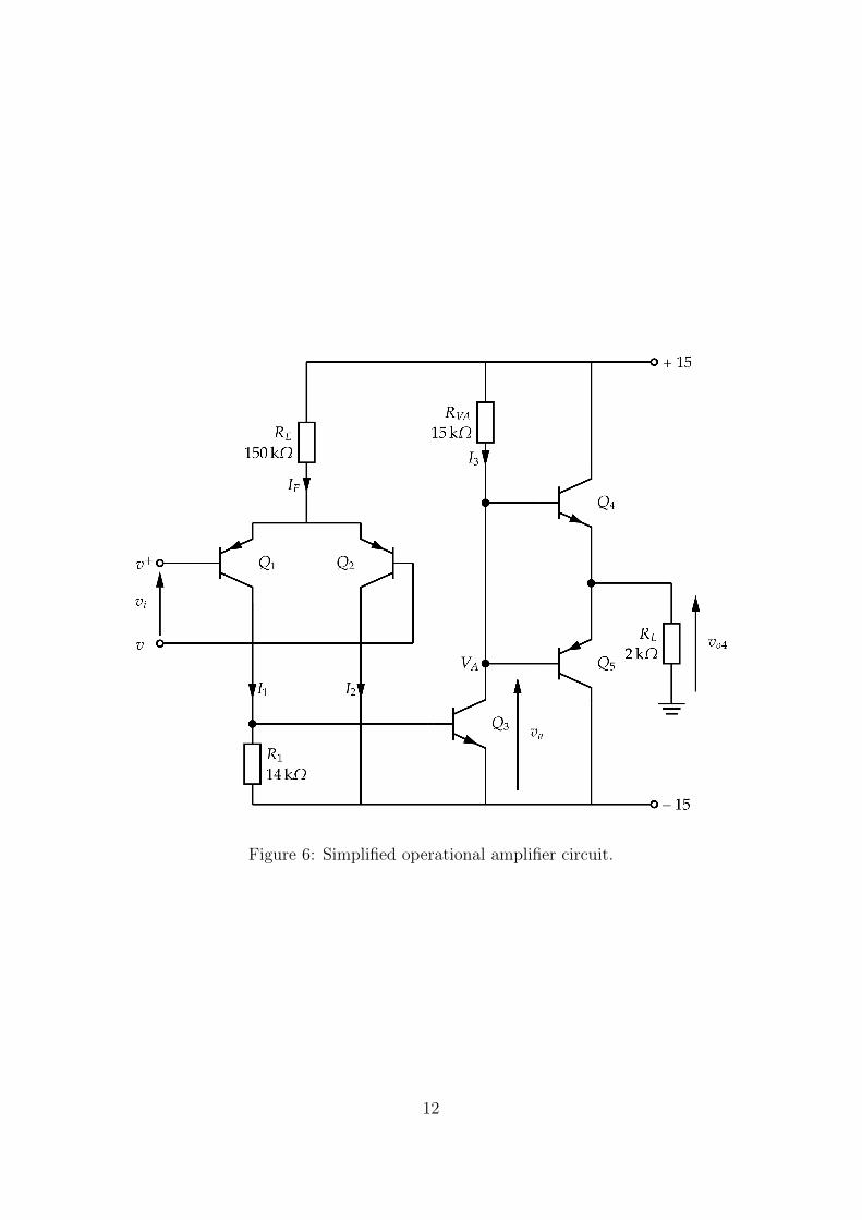
Figure 6: Simplified operational amplifier circuit.
12
Question 7: Push Pull Emitter Follower1. Concisely describe the cause of crossover distortion in class B push-pull
amplifiers.
2. Use a sketch to show the effects of crossover distortion on a triangle orsinusoidal waveform, taking particular care with your representation of thecrossover region.
3. Sketch a circuit diagram of a voltage amplifier and push pull stage whichlargely overcomes the problems of crossover distortion and describe theoperation of your circuit.
4. Calculate the quiescent power dissipation in one of the output transistorsin your circuit.
5. Calculate the average power dissipated in the load resistor of your circuit.
6. Derive expressions for the instantaneous power dissipation in one of the out-put transistors. You may assume that the power dissipated in a transistor isthe product of IC and VCE which will both vary approximately sinusoidallygiven a sinusoidal input. Hint: this involves some integration of sines andcosines.
7. Using your derivation find the signal voltage amplitude across the outputwhich results in the highest power dissipation in the transistor.
8. Show that the highest possible efficiency of this circuit is approximately70%.
9. The push-pull stage may operate in class C, B or A depending on thequiescent current flowing in the output transistors, which in turn is relatedto the voltage between the bases of the two output transistors. Sketch theload voltage and collector current waveforms of the two output transistorsfor each class, noting the salient features.
10. For each class of operation above, what angle of current conduction existsin each class and what approximate range of voltages must exist betweenthe bases of the output transistors?
13
Question 8: Common Base TransimpedanceAmplifier with DC servoDownload the journal paper at http://dx.doi.org/10.1088/0957-0233/23/
12/125901. You may need VPN, see http://www.shef.ac.uk/cics/vpn fordetails. Describe how the transimpedance amplifier in Figure 6 of this paperworks. Develop the DC conditions and the small signal parameters of the commonbase stage driven by the photodiode.
Question 9: A Charge Amplifier for X-RayDetectionThis question relates to a charge amplifier - its output votlage is porportional tothe integral of the input current. This sort of circuit is often used to interfacecertain kinds of semiconductor detectors with signal processing hardware (suchas multi-channel analysers). The circuit has a very high input impedace and lowoutput impedance.
1. Describe in words how the circuit acts to stabilise its DC conditions. Inso doing identify the circuit building blocks and describe the low frequencyfeedback (ignore C3).
2. Calculate the DC conditions (currents through and voltages across all com-ponents (except C3). Assume that for the JFET ID = 10 mA at VGS =0 V. Assume the small signal current gain of all the BJTs is 100.
3. Postulate the purpouse of C2. What is it likely to form a time constantwith?
4. What is C3’s job in this circuit? It may help to think about the inputas being short duration pulses of current sepperated by long periods ofnothing. This would represent an x-ray generating a number of electronhole pairs as it passes through the detector, these become the pulse. Theinput impedance is very large so pushing current onto the gate will have tocharge up or discharge some capacitors (including those internal to Q1) thechange in gate voltage will act to turn Q1 on or off somewhat. This signalwill propogate through the amplifier until it reaches the output (which isalso the right hand side of C3). Another way to look at it is to ask whatwill happen if I keep putting charge onto the gate and it doesn’t leave. Theamplifier will saturate, so how can I avoid this?
14

Q1Q2
R1
680 Ω
Q3
R6
1000 Ω
R2
20 kΩ
R7
3.9 kΩ
R5
10 kΩ
Q4 Q5
R8
20 kΩ
R3
10 kΩ
R4
5.1 kΩ
Q2
C2
100 nF
C3
0.2 pF
In
-15 V
+15 V
C1
100 nFR9
50 Ω
C6
100 nF
Out
Figure 7: Akeel’s charge amplifier.
15
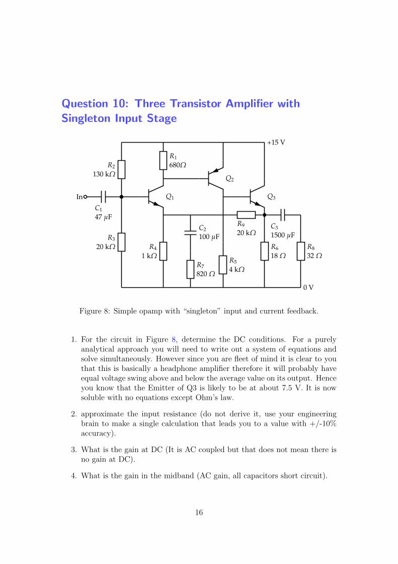
Question 10: Three Transistor Amplifier withSingleton Input Stage
C1
47 µF
In
R3
20 kΩ
R2
130 kΩ
Q1
R4
1 kΩ
R1
680Ω
Q2
R5
4 kΩ
C2
100 µF
R7
820 Ω
Q3
R6
18 Ω
R9
20 kΩC3
1500 µF
R8
32 Ω
+15 V
0 V
Figure 8: Simple opamp with “singleton” input and current feedback.
1. For the circuit in Figure 8, determine the DC conditions. For a purelyanalytical approach you will need to write out a system of equations andsolve simultaneously. However since you are fleet of mind it is clear to youthat this is basically a headphone amplifier therefore it will probably haveequal voltage swing above and below the average value on its output. Henceyou know that the Emitter of Q3 is likely to be at about 7.5 V. It is nowsoluble with no equations except Ohm’s law.
2. approximate the input resistance (do not derive it, use your engineeringbrain to make a single calculation that leads you to a value with +/-10%accuracy).
3. What is the gain at DC (It is AC coupled but that does not mean there isno gain at DC).
4. What is the gain in the midband (AC gain, all capacitors short circuit).
16

5. list the major problems with the circuit and explain how they arrise. Whyare real amplifiers not made like this? Think about input and outputimpedance, gain, distortion etc.
6. If you could only change one thing to improve the performance of the circuitwhat would it be?
7. how hot is Q3 likely to get if it is a 2N3055 in a TO3 metal package withouta heatsink, is that acceptable? Why?
8. I described it as series–shunt feedback what does that actually mean? Whatimpact does the ‘mode’ of feedback have on the circuit performance? (Youwill need to do some serious background reading in Grey Hurst Lewis andMeyer - it’s to do with input and output impedance).
9. Since you’ve got Grey open...probably around page 583 if you’re in the 5thedition. Teach yourself how to use signal flow graphs to analyse circuitswith feedback. Apply the technique to the circuit in this question.
10. Replace the input transistor with a JFET, 2N3819. Re-design the circuitto perform the same function. The input stage biasing resistors can beremoved and the gate of the JFET can float at 0 V.
11. Use LTSPICE to compare the input impedance of the two circuits.
12. Use the LoopGain2.asc example file in the “Educational” directory of LT-SPICE to assess the open loop gain of this amplifier. Add compensationbetween collector and base of Q2 observe the effects of changing the domi-nant pole frequency on the open loop gain for several values of capacitor (try100 pF to start). Inspect the open loop gain and phase margins, compensateit to ensure stability.
17