ee247 lecture 25 - ee247/fa05/lectures/l25_3.pdfee247 lecture 25 • administrative ... “the...
TRANSCRIPT

EECS 247 Lecture 25: Oversampling Data Converters © 2005 H. K. Page 1
EE247Lecture 25
• Administrative– EE247 Final exam:
– Date: Tues. Dec. 13th
– Time: 12:30pm-3:30pm– Location: 285 Cory Hall
• Closed book/course notes• No calculators/cell phones/PDAs/computers• Bring one 8x11 paper with your own notes• Final exam covers the entire course material unless
specified
EECS 247 Lecture 25: Oversampling Data Converters © 2005 H. K. Page 2
EE247Lecture 25
• Oversampled ADCs– 2nd order ΣΔ modulator
• Practical implementation– Effect of various nonidealities on the ΣΔ
performance
• Higher order ΣΔ modulators– Cascaded modulators (multi-stage)– Single-loop single-quantizer modulators
with multi-order filtering in the forward path

EECS 247 Lecture 25: Oversampling Data Converters © 2005 H. K. Page 3
Oversampled ADCsLast Lecture
Oversampled ADCs:–Allows trading speed for resolution – No stringent requirements imposed on analog building blocks –Takes advantage of low cost, low power digital filtering–Relaxed transition band requirements for analog anti-aliasing
filters–Further reduction of baseband quantization noise power by
combining oversampling with clever use of feedback• By simply increasing oversampling ratio: 2X increase in sampling ratio
0.5-bit increase in resolution• Embedding the quantizer in a 1st order feedback loop 1.5-bit increase is resolution per 2x increase in sampling rate
• Adding a 2nd loop 2.5-bit increase per 2x increase in sampling rate
EECS 247 Lecture 25: Oversampling Data Converters © 2005 H. K. Page 4
ΣΔ ImplementationPractical Design Considerations
• Internal nodes scaling & clipping
• Finite opamp gain & linearity
• Capacitor ratio errors
• KT/C noise
• Opamp noise
• Power dissipation considerations

EECS 247 Lecture 25: Oversampling Data Converters © 2005 H. K. Page 5
Switched-Capacitor Implementation 2nd Order ΣΔNodes Scaled for Maximum Dynamic Range
• Modification (gain of ½ in front of integrators) reduce & optimize required signal range at the integrator outputs ~ 1.7x input full-scale (Δ)
Ref: B.E. Boser and B.A. Wooley, “The Design of Sigma-Delta Modulation A/D Converters,” IEEE J. Solid-State Circuits, vol. 23, no. 6, pp. 1298-1308, Dec. 1988.
EECS 247 Lecture 25: Oversampling Data Converters © 2005 H. K. Page 6
2nd Order ΣΔ ModulatorSwitched-Capacitor Implementation
C2=2C1
• The ½ loss in front of each integrator implemented by choice of:

EECS 247 Lecture 25: Oversampling Data Converters © 2005 H. K. Page 7
2nd Order ΣΔEffect of Integrator Maximum Signal Handling Capability on SNR
• Effect of 1st Integrator maximum signal handling capability on converter SNRRef: B.E. Boser and B.A. Wooley, “The Design of Sigma-Delta Modulation A/D Converters,”
IEEE J. Solid-State Circuits, vol. 23, no. 6, pp. 1298-1308, Dec. 1988.
1st integrator maximum signal handling:1.4, 1.5,1.6, and 1.7X Δ
EECS 247 Lecture 25: Oversampling Data Converters © 2005 H. K. Page 8
2nd Order ΣΔEffect of Integrator Maximum Signal Handling Capability on SNR
• Effect of 2nd Integrator maximum signal handling capability on SNRRef: B.E. Boser and B.A. Wooley, “The Design of Sigma-Delta Modulation A/D Converters,”
IEEE J. Solid-State Circuits, vol. 23, no. 6, pp. 1298-1308, Dec. 1988.
2nd integrator maximum signal handling:0.75,1,1.25, 1.5, and 1.75X Δ

EECS 247 Lecture 25: Oversampling Data Converters © 2005 H. K. Page 9
2nd Order ΣΔEffect of Integrator Finite DC Gain
Vi
-
+
φ1 φ2
aVo
Cs
CI( )
( )
1
1
1
1
1
1
111
ideal
Finit DC Gain
Cs zH zCI z
a zCsaCs CIH zCI
a zCsaCI
−
−
−
−
= ×−⎛ ⎞⎜ ⎟⎜ ⎟
+ +⎜ ⎟⎝ ⎠= ×⎛ ⎞⎜ ⎟+− ⎜ ⎟
+ +⎜ ⎟⎝ ⎠
a opamp gain at DC
Integrator
EECS 247 Lecture 25: Oversampling Data Converters © 2005 H. K. Page 10
2nd Order ΣΔEffect of Integrator Finite DC Gain
• Low integrator DC gain Increase in total in-band noise • Can be shown: If a > M (oversampling ratio) Insignificant degradation in
SNR• Normally DC gain designed to be >> M in order to suppress nonlinearities
f0 /a
a
0P1 aω=
0ω
a
( )log H sIdeal Integ. (a=infinite)
Integrator magnitude response
Max signal level

EECS 247 Lecture 25: Oversampling Data Converters © 2005 H. K. Page 11
2nd Order ΣΔEffect of Integrator Finite DC Gain
• Example: a =2M 0.4dB degradation in SNRRef: B.E. Boser and B.A. Wooley, “The Design of Sigma-Delta Modulation A/D Converters,”
IEEE J. Solid-State Circuits, vol. 23, no. 6, pp. 1298-1308, Dec. 1988.
M / a
EECS 247 Lecture 25: Oversampling Data Converters © 2005 H. K. Page 12
2nd Order ΣΔEffect of Comparator Non-Idealities on SD Performance
1-bit A/D Single comparator• Speed must be adequate for the operating sampling rate• Input referred offset- feedback loop suppresses the effect
ΣΔ performance not sensitive to input referred offset• Input referred noise- same as offset• Hysteresis= Minimum overdrive required to change the output

EECS 247 Lecture 25: Oversampling Data Converters © 2005 H. K. Page 13
2nd Order ΣΔComparator Hysteresis
Hysteresis= Minimum overdrive required to change the output
EECS 247 Lecture 25: Oversampling Data Converters © 2005 H. K. Page 14
2nd Order ΣΔComparator Hysteresis
Comparator hysteresis < Δ/40 does not affect SNRE.g. Δ=1V, comparator offset/hysteresis up to 25mV tolerable

EECS 247 Lecture 25: Oversampling Data Converters © 2005 H. K. Page 15
2nd Order ΣΔEffect Overall Integrator Gain Inaccuracy
• Gain of ½ in front of integrators determined by ratio of C1/C2
• Effect of inaccuracy in ratio of C1/C2 inspected by simulation
EECS 247 Lecture 25: Oversampling Data Converters © 2005 H. K. Page 16
2nd Order ΣΔEffect of Integrator Overall Gain Inaccuracy
• Simulation show gain can vary by 20% w/o loss in performanceConfirms insensitivity of ΣΔ to component variations
• Note that for gain >0.65 system becomes unstable & SNR drops rapidly
Unstable
EECS 247 Lecture 25: Oversampling Data Converters © 2005 H. K. Page 17
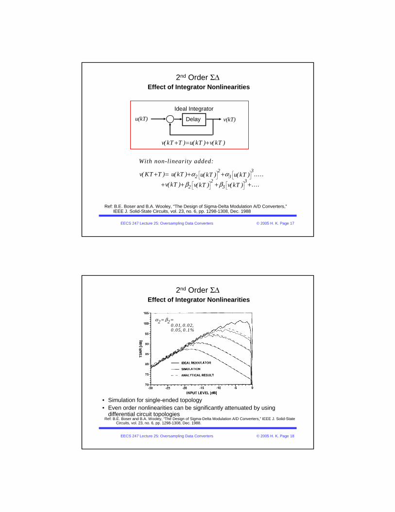
2nd Order ΣΔEffect of Integrator Nonlinearities
2 32 3
2 32 3
v( kT T ) u(kT ) v( kT )
With non-linearity added:
v( KT T ) u(kT ) .....u(kT ) u(kT )v( kT ) ....v( kT ) v( kT )
α αβ β
⎡ ⎤ ⎡ ⎤⎣ ⎦ ⎣ ⎦
⎡ ⎤ ⎡ ⎤⎣ ⎦ ⎣ ⎦
+ = +
+ = + +
+ + + +
Ref: B.E. Boser and B.A. Wooley, “The Design of Sigma-Delta Modulation A/D Converters,” IEEE J. Solid-State Circuits, vol. 23, no. 6, pp. 1298-1308, Dec. 1988
Delay
Ideal Integrator
u(kT) v(kT)
EECS 247 Lecture 25: Oversampling Data Converters © 2005 H. K. Page 18
2nd Order ΣΔEffect of Integrator Nonlinearities
Ref: B.E. Boser and B.A. Wooley, “The Design of Sigma-Delta Modulation A/D Converters,” IEEE J. Solid-State Circuits, vol. 23, no. 6, pp. 1298-1308, Dec. 1988.
• Simulation for single-ended topology• Even order nonlinearities can be significantly attenuated by using
differential circuit topologies
2 20.01, 0 .02,0.05, 0.1%
α β= =

EECS 247 Lecture 25: Oversampling Data Converters © 2005 H. K. Page 19
2nd Order ΣΔEffect of Integrator Nonlinearities
Ref: B.E. Boser and B.A. Wooley, “The Design of Sigma-Delta Modulation A/D Converters,” IEEE J. Solid-State Circuits, vol. 23, no. 6, pp. 1298-1308, Dec. 1988.
• Simulation for single-ended topology• Odd order nonlinearities (3rd in this case)
3 30.05, 0.2, 1%
α β= = 6dB =1-Bit
EECS 247 Lecture 25: Oversampling Data Converters © 2005 H. K. Page 20
2nd Order ΣΔEffect of KT/C noise
• For the example of digital audio with 16-bit (100dB) & M=256Cs=1pF 6μVrms noiseIf FS=2Vp-p-d then thermal noise @ -101dB degrades overall SNR by < 3dBCs=1pF, CI=2pF small capacitor area compared to Nyquist ADCSince thermal noise provides some level of dithering better not choose much larger capacitors!
Vi
-
+
φ1 φ2
Vo
Cs
CI2
2
20
2
1/ 2 4/ 2
Total in-band noise:
4
2
n
n
n input referred
KTvCs
kT kTv fCs fs Cs fs
kTv fCs fs
kTCs M
−
=
= × =×
= ××
=×

EECS 247 Lecture 25: Oversampling Data Converters © 2005 H. K. Page 21
2nd Order ΣΔEffect of Finite Opamp Bandwidth
Input/Output z-transformVi+
Cs-
+ Vo
CIφ1 φ2
Vi-Unity-gain-freq.= fu =1/τ
Vo
φ2
T=1/fs
settlingerror
time
Assumptions: Opamp does not slewOpamp has only one pole exponential settling
EECS 247 Lecture 25: Oversampling Data Converters © 2005 H. K. Page 22
2nd Order ΣΔEffect of Finite Opamp Bandwidth
ΣΔ does not require high opamp bandwidth fu > 2fs adequate

EECS 247 Lecture 25: Oversampling Data Converters © 2005 H. K. Page 23
2nd Order ΣΔEffect of Slew Limited Settling
φ1
φ2
Vo-real
Vo-ideal
Clock
Slewing Slewing
EECS 247 Lecture 25: Oversampling Data Converters © 2005 H. K. Page 24
2nd Order ΣΔEffect of Slew Limited Settling
Assumption: Opamp settling includes a single-pole setting of τ =1/2fs + slewing
Low slew rate degrades SNR rapidly- increases quantization noise and causes signal distortionMinimum slew rate of 1.2 (Δ x fs) required
Input Signal = -5dBT/τ =2

EECS 247 Lecture 25: Oversampling Data Converters © 2005 H. K. Page 25
Design Phase Simulations• Design of oversampled ADCs requires simulation of extremely long data
traces
• SPICE type simulators:
–Normally used to test for gross circuit errors only
–Too slow and inaccurate for performance verification
• Typically, behavioral modeling is used in MATLAB-like environments
• Circuit non-idealities either computed or found by using SPICE at subcircuit level
• Non-idealities introduced in the behavioral model one-by-one first to fully understand the effect of each individually
• Next step is to add as many of the non-idealities simultaneously as possible to verify whether there are interaction among non-idealities
EECS 247 Lecture 25: Oversampling Data Converters © 2005 H. K. Page 26
Modulator Testing• Should make provisions for testing the modulator (AFE) separate from the
decimator (digital back-end)
• Data acquisition board used to collect 1-bit digital output at fs rate
• Analyze data in a PC environment or dedicated test equipment in manufacturing environments can be used
• Need to run DFT on the collected data and also make provisions to perform the function of digital decimation filter in software
• Typically, at this stage, parts of the design phase behavioral modeling effort can be utilized
• Good testing strategy vital for debugging/improving challenging designs
AFE Data Acq.
PC Matlab
fs
FilteredSinwave
EECS 247 Lecture 25: Oversampling Data Converters © 2005 H. K. Page 27
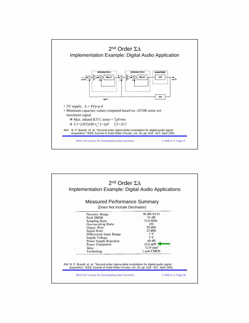
2nd Order ΣΔImplementation Example: Digital Audio Application
• 5V supply, Δ = 4Vp-p-d• Minimum capacitor values computed based on -107dB noise wrt
maximum signal Max. inband KT/C noise = 7μVrmsC1=(2kT)/(M vn
2 )=1pF C2=2C1Ref: B. P. Brandt, et. al, "Second-order sigma-delta modulation for digital-audio signal
acquisition," IEEE Journal of Solid-State Circuits, vol. 26, pp. 618 - 627, April 1991.
EECS 247 Lecture 25: Oversampling Data Converters © 2005 H. K. Page 28
2nd Order ΣΔImplementation Example: Digital Audio Applications
Ref: B. P. Brandt, et. al, "Second-order sigma-delta modulation for digital-audio signal acquisition," IEEE Journal of Solid-State Circuits, vol. 26, pp. 618 - 627, April 1991.
Measured Performance Summary(Does Not Include Decimator)

EECS 247 Lecture 25: Oversampling Data Converters © 2005 H. K. Page 29
2nd Order ΣΔImplementation Example: Digital Audio Applications
Ref: B. P. Brandt, et. al, "Second-order sigma-delta modulation for digital-audio signal acquisition," IEEE Journal of Solid-State Circuits, vol. 26, pp. 618 - 627, April 1991.
Measured SNDRM=256, 0dB=4Vp-p-dfsampling: 12.8MHzSignal Frequency: 2.8kHz
OptimumSNR @ -3dB
wrt to Δ
EECS 247 Lecture 25: Oversampling Data Converters © 2005 H. K. Page 30
2nd Order ΣΔImplementation Example: Digital Audio Applications
Ref: B. P. Brandt, et. al, "Second-order sigma-delta modulation for digital-audio signal acquisition," IEEE Journal of Solid-State Circuits, vol. 26, pp. 618 - 627, April 1991.

EECS 247 Lecture 25: Oversampling Data Converters © 2005 H. K. Page 31
2nd Order ΣΔImplementation Example: Digital Audio Applications
Measured & simulated spurious tones performance as a function of DC input signal Sampling rate=12.8MHz, M=256
Ref: B. P. Brandt, et. al, "Second-order sigma-delta modulation for digital-audio signal acquisition," IEEE Journal of Solid-State Circuits, vol. 26, pp. 618 - 627, April 1991.
EECS 247 Lecture 25: Oversampling Data Converters © 2005 H. K. Page 32
2nd Order ΣΔImplementation Example: Digital Audio Applications
Measured & simulated noise tone performance for near zero DC input of0.00088Δ
Sampling rate=12.8MHz, M=256Ref: B. P. Brandt, et. al, "Second-order sigma-delta modulation for digital-audio signal acquisition," IEEE Journal of Solid-State Circuits, vol. 26, pp. 618 - 627, April 1991.

EECS 247 Lecture 25: Oversampling Data Converters © 2005 H. K. Page 33
2nd Order ΣΔImplementation Example: Digital Audio Applications
Measured & simulated worst-case noise tone @ DC input of 0.00088ΔBoth indicate maximum tone @ 22.5kHz around -100dB level
Ref: B. P. Brandt, et. al, "Second-order sigma-delta modulation for digital-audio signal acquisition," IEEE Journal of Solid-State Circuits, vol. 26, pp. 618 - 627, April 1991.
EECS 247 Lecture 25: Oversampling Data Converters © 2005 H. K. Page 34
2nd Order ΣΔImplementation Example: Integrator Opamp
Class A/B opamp High slew-rate S.C. common-mode feedback
Input referred noise (both thermal and 1/f) important for high resolution performance
Minimum required DC gain> M=256 , usually DC gain designed to be much higher to suppress nonlinearities (particularly, for class A/B amps
Minimum required slew rate of 1.2(Δfs) 65V/usec
Minimum opamp settling time constant 1/2fs~30nsec
Ref: B. P. Brandt, et. al, "Second-order sigma-delta modulation for digital-audio signal acquisition," IEEE Journal of Solid-State Circuits, vol. 26, pp. 618 - 627, April 1991.

EECS 247 Lecture 25: Oversampling Data Converters © 2005 H. K. Page 35
2nd Order ΣΔImplementation Example: Comparator
Comparator simple design
Minimum acceptable hysteresis or offset (based on analysis) Δ/40 ∼ 100mV
Ref: B. P. Brandt, et. al, "Second-order sigma-delta modulation for digital-audio signal acquisition," IEEE Journal of Solid-State Circuits, vol. 26, pp. 618 - 627, April 1991.
EECS 247 Lecture 25: Oversampling Data Converters © 2005 H. K. Page 36
2nd Order ΣΔImplementation Example: Subcircuit Performance
Our computed Over-Design Factorminimum requiredDC Gain 48dB x8Unity-gain freq =2fs=25MHz x2Slew rate = 65V/usec x5
Output range 1.7Δ=6.8V! X0.9
Settling time constant= 30nsec x4
Comparator offset 100mV x7
Ref: B. P. Brandt, et. al, "Second-order sigma-delta modulation for digital-audio signal acquisition," IEEE Journal of Solid-State Circuits, vol. 26, pp. 618 - 627, April 1991.

EECS 247 Lecture 25: Oversampling Data Converters © 2005 H. K. Page 37
Higher Order ΣΔ Modulators
• Extending ΣΔ Modulators to higher orders by adding integrators in the forward path (similar to 2nd order)
Issues with stability• Two different architectural approaches used
to implement ΣΔ modulators of order >2– Single-loop single-quantizer modulators with multi-
order filtering in the forward path
– Cascade of lower order modulators (multi-stage)
EECS 247 Lecture 25: Oversampling Data Converters © 2005 H. K. Page 38
Higher Order ΣΔ ModulatorsMult-Order Filter
• Zeros of NTF (poles of H(z)) can be positioned to suppress baseband noise spectrum
• Main issue Loop stability for 3rd and higher orders
( ) 1( ) ( ) ( )1 ( ) 1 ( )
H zY z X z E zH z H z
= ++ +
Σ
E(z)
X(z) Y(z)( )H z Σ
Y( z ) 1NTF
E( z ) 1 H( z )= =
+

EECS 247 Lecture 25: Oversampling Data Converters © 2005 H. K. Page 39
Higher Order ΣΔ ModulatorsCascaded Modulators
• Cascade two or more stable ΣΔ stages• Quantization error of each stage is quantized by the
succeeding stage and subtracted digitally • Order of noise shaping equals sum of the orders of
the stages• Quantization noise cancellation depends on the
precision of analog signal paths• Quantization noise further randomized less limit
cycle oscillation problems• Typically, no potential instability
EECS 247 Lecture 25: Oversampling Data Converters © 2005 H. K. Page 40
2-Stage Cascaded ΣΔ Modulators
• Main ΣΔ quantizes the signal • The quantization error is then quantized by the 2nd quantizer • The quantized error is then subtracted from the results in the digital
domain

EECS 247 Lecture 25: Oversampling Data Converters © 2005 H. K. Page 41
2nd Order (1-1) Cascaded ΣΔ Modulators
2nd order noise shaping
EECS 247 Lecture 25: Oversampling Data Converters © 2005 H. K. Page 42
3rd Order Cascaded ΣΔ Modulators
• Can implement 3rd
order noise shaping with 1-1-1
• This is also called MASH (multi-stage noise shaping)

EECS 247 Lecture 25: Oversampling Data Converters © 2005 H. K. Page 43
3rd Order (2-1) Cascaded ΣΔ Modulators
3rd order noise shaping
Advantages of 2-1 cascade:• Low sensitivity to
precision of analog paths• Low spurious noise
tones• No potential instability
EECS 247 Lecture 25: Oversampling Data Converters © 2005 H. K. Page 44
Sensitivity of (1-1-1) Cascaded ΣΔ Modulatorsto Matching of Analog & Digital Gains
Accuracy of < 0.1%2dB loss in DR

EECS 247 Lecture 25: Oversampling Data Converters © 2005 H. K. Page 45
Sensitivity of (2-1) Cascaded ΣΔ Modulatorsto Matching Error
Accuracy of < +−3%2dB loss in DR
Main advantage of 2-1 cascade compared to 1-1-1 topology:• Low sensitivity to precision of analog paths (over one order of
magnitude!)
EECS 247 Lecture 25: Oversampling Data Converters © 2005 H. K. Page 46
2-1 Cascaded ΣΔ Modulators
Accuracy of < +−3%2dB loss in DR
Ref: L. A. Williams III and B. A. Wooley, "A third-order sigma-delta modulator with extended dynamic range," IEEE Journal of Solid-State Circuits, vol. 29, pp. 193 - 202, March 1994.

EECS 247 Lecture 25: Oversampling Data Converters © 2005 H. K. Page 47
2-1 Cascaded ΣΔ Modulators
Effect of gain parameters on signal-to-noise ratio
EECS 247 Lecture 25: Oversampling Data Converters © 2005 H. K. Page 48
Comparison of 2nd order & Cascaded (2-1) ΣΔ Modulator
5.2mm20.39mm2Active Area47.2mW13.8mWPower Dissipation
8Vppd5V supply
4Vppd5V supply
Differential input range
128 (theoretical SNR=128dB)
256 (theoretical SNR=109dB)
Oversampling rate98dB94dBPeak SNDR104dB (17-bits)98dB (16-bits)Dynamic Range(2+1) Order2nd orderArchitectureWilliams, JSSC 3/94Brandt ,JSSC 4/91Reference
Digital Audio Application, fN=50kHz

EECS 247 Lecture 25: Oversampling Data Converters © 2005 H. K. Page 49
2-1 Cascaded ΣΔ ModulatorsMeasured Dynamic Range Versus Oversampling Ratio
Ref: L. A. Williams III and B. A. Wooley, "A third-order sigma-delta modulator with extended dynamic range," IEEE Journal of Solid-State Circuits, vol. 29, pp. 193 - 202, March 1994.
3dB/Octave
21dB/Octave
EECS 247 Lecture 25: Oversampling Data Converters © 2005 H. K. Page 50
Summary•Oversampled ADCs decouple SQNR from circuit complexity and accuracy
•If a 1-Bit DAC is used, the converter is inherently linear—independent of component matching
•Typically, used for high resolution & low frequency applications – e.g. digital audio
•2nd order ΣΔ used extensively due to lower levels of limit cycle related spurious tones
• ΣΔ modulators of order greater than 2:– Single-loop, single-quantizer modulators with multi-order filtering in the
forward path– Cascaded (multi-stage) modulators
EECS 247 Lecture 25: Oversampling Data Converters © 2005 H. K. Page 51
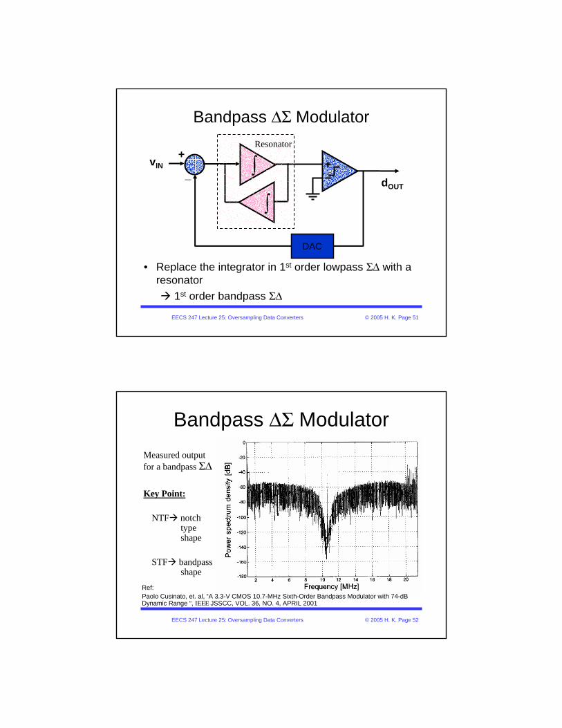
Bandpass ΔΣ Modulator
+
_vIN
dOUT
∫
DAC
∫
• Replace the integrator in 1st order lowpass ΣΔ with a resonator
1st order bandpass ΣΔ
Resonator
EECS 247 Lecture 25: Oversampling Data Converters © 2005 H. K. Page 52
Bandpass ΔΣ ModulatorMeasured output for a bandpass ΣΔ
Key Point:
NTF notch type shape
STF bandpass shape
Ref: Paolo Cusinato, et. al, “A 3.3-V CMOS 10.7-MHz Sixth-Order Bandpass Modulator with 74-dB Dynamic Range “, ΙΕΕΕ JSSCC, VOL. 36, NO. 4, APRIL 2001

EECS 247 Lecture 25: Oversampling Data Converters © 2005 H. K. Page 53
Bandpass ΣΔ Modulator Dynamic RangeAs a Function of Modulator Order (K)
• Bandpass ΣΔ resolution for order K is the same as lowpass ΣΔ resolution with order L= K/2
K=415dB/Octave
K=621dB/Octave
K=29dB/Octave
EECS 247 Lecture 25: Oversampling Data Converters © 2005 H. K. Page 54
Example: Sixth-Order Bandpass ΣΔ Modulator
Ref: Paolo Cusinato, et. al, “A 3.3-V CMOS 10.7-MHz Sixth-Order Bandpass Modulator with 74-dB Dynamic Range “, ΙΕΕΕ JSSCC, VOL. 36, NO. 4, APRIL 2001
Simulated noise transfer function Simulated signal transfer function

EECS 247 Lecture 25: Oversampling Data Converters © 2005 H. K. Page 55
Bandpass ΣΔ Characteristics• Oversampling ratio defined as fs/2B
where B = bandpass filter bandwidth• Typically, sampling frequency is chosen
to be 4xfcenter where fcenter=bandpass filter center frequency
• STF has a bandpass shape while NTF has a notch shape
• To achieve same resolution as lowpass, needs twice as many integrators