ee204 notes 7 - u of s engineering half-wave and full-wave configurations were considered during the...
TRANSCRIPT

EE204 Basic Electronics and Electric Power Course Notes
© Denard Lynch 2012 Page 1 of 22 Nov 14, 2012
Energy Sources and Power Conversion This Section will discuss some of the ways energy is provided to electronic and electromechanical devices. In most cases, the voltages required for various purposes are varied and usually different than the available source. AC sources must be converted to DC, voltages must be changed to supply electronic controllers (5VDC, 3.3VDC), solenoid valves, motors, relays (12VDC, 24VDC etc.). In other cases, batteries and other forms of storage devices are used to supply stored energy, or devices like generators and photovoltaic cells are used to convert mechanical, wind or solar energy to electrical energy. In all these cases, there is usually a need to control the output voltage of these generators or converters with certain tolerances in order to ensure the proper functioning of the electric devices. Topics that will be covered, at least to some extent, include:
1. Power Conversion a) AC (mains) Power Supplies
i. Half wave rectifiers ii. Full wave rectifiers
iii. Switching supplies b) Filtering of Rectified or Switched Power Supplies c) Voltage Regulation
i. Linear Regulators ii. Regulated Switch Mode Power Supplies (SMPS)
2. Power Generation and Storage a) Mechanical Generators
i. Wind energy b) Batteries
i. Lead-acid ii. Carbon-Zinc
iii. NiCad iv. NiMH v. LiPo
c) Solar Cells
EE204 Basic Electronics and Electric Power Course Notes
© Denard Lynch 2012 Page 2 of 22 Nov 14, 2012
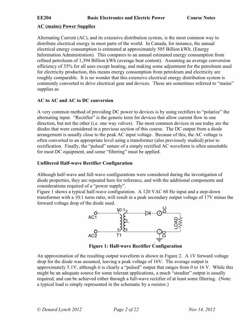
AC (mains) Power Supplies Alternating Current (AC), and its extensive distribution system, is the most common way to distribute electrical energy in most parts of the world. In Canada, for instance, the annual electrical energy consumption is estimated at approximately 505 Billion kWh. (Energy Information Administration). This compares to an annual estimated energy consumption from refined petroleum of 1,394 Billion kWh (average heat content). Assuming an average conversion efficiency of 35% for all uses except heating, and making some adjustment for the petroleum used for electricity production, this means energy consumption from petroleum and electricity are roughly comparable. It is no wonder that this extensive electrical energy distribution system is commonly converted to drive electrical gear and devices. These are sometimes referred to “mains” supplies as AC to AC and AC to DC conversion A very common method of providing DC power to devices is by using rectifiers to “polarize” the alternating input. “Rectifier” is the generic term for devices that allow current flow in one direction, but not the other (i.e. one way valves). The most common devices in use today are the diodes that were considered in a previous section of this course. The DC output from a diode arrangement is usually close to the peak AC input voltage. Because of this, the AC voltage is often converted to an appropriate level using a transformer (also previously studied) prior to rectification. Finally, the “pulsed” nature of a simply rectified AC waveform is often unsuitable for most DC equipment, and some “filtering” must be applied. Unfiltered Half-wave Rectifier Configuration Although half-wave and full-wave configurations were considered during the investigation of diode properties, they are repeated here for reference, and with the additional components and considerations required of a “power supply”. Figure 1 shows a typical half-wave configuration. A 120 VAC 60 Hz input and a step-down transformer with a 10:1 turns ratio, will result in a peak secondary output voltage of 17V minus the forward voltage drop of the diode used.
Figure 1: Half-wave Rectifier Configuration
An approximation of the resulting output waveform is shown in Figure 2. A 1V forward voltage drop for the diode was assumed, leaving a peak voltage of 16V. The average output is approximately 5.1V, although it is clearly a “pulsed” output that ranges from 0 to 16 V. While this might be an adequate source for some tolerant applications, a much “steadier” output is usually required, and can be achieved either through a full-wave rectifier of at least some filtering. (Note: a typical load is simply represented in the schematic by a resistor.)
T1
DCDC
.
..
.
10:12
4
1
5
3
LOAD
AC1
AC2

EE204 Basic Electronics and Electric Power Course Notes
© Denard Lynch 2012 Page 3 of 22 Nov 14, 2012
Figure 2: Half-wave Rectified 60 Hz AC
A full-wave bridge rectifier configuration utilizes the full AC cycle by arranging four diodes as shown in Figure 3. This schematic again shows a step-down transformer with a 10:1 turns ratio, resulting in a peak output of 15V from a 120 VAC source if we consider a 1V forward voltage drop across each of the two diodes in current path for each half of the cycle (17V peak – 2V).
Figure 3: Full-wave Bridge Rectifier Configuration
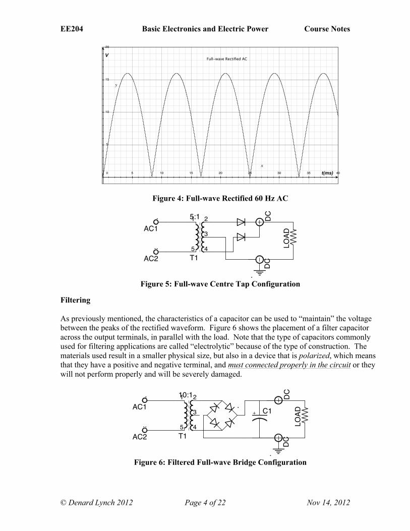
The output waveform for a full-wave configuration is shown in Figure 4, although in this case idea diodes were assumed, so the peak output is shown as 17V. The output, while still “pulsed”, has an average output voltage of (2/π x17V) 10.8V. This type of output is often adequate for powered DC motors, solenoids or relays, but would not be “smooth” enough for electronic equipment. An alternate way of providing a full-wave output with only two diodes instead of four is shown in Figure 5. This configuration also has the slight advantage that there is only one diode voltage drop in series with the load for each half cycle, but the disadvantage that a centre-tapped secondary is required on the transformer. Note also that the transformer in Figure 5 has an overall 5:1 turns ratio to achieve approximately the same output voltage (It is effectively a 10:1 ratio for each “half” of the secondary so that the 17V peak is impressed across the diode during each half cycle). As we shall see, we can use a capacitor to provide some filtering, but we have yet to deal with the issue of “regulation” – keeping the output constant in the face of a varying load or source supply.
0 5 10 15 20 25 30 35 40
5
10
15
20
V
t(ms)
Half-wave Rectified AC
T1
DCDC
.
..
.10:12
4
1
5
3LO
AD
AC1
AC2
.
EE204 Basic Electronics and Electric Power Course Notes
© Denard Lynch 2012 Page 4 of 22 Nov 14, 2012
Figure 4: Full-wave Rectified 60 Hz AC
Figure 5: Full-wave Centre Tap Configuration
Filtering As previously mentioned, the characteristics of a capacitor can be used to “maintain” the voltage between the peaks of the rectified waveform. Figure 6 shows the placement of a filter capacitor across the output terminals, in parallel with the load. Note that the type of capacitors commonly used for filtering applications are called “electrolytic” because of the type of construction. The materials used result in a smaller physical size, but also in a device that is polarized, which means that they have a positive and negative terminal, and must connected properly in the circuit or they will not perform properly and will be severely damaged.
Figure 6: Filtered Full-wave Bridge Configuration
0 5 10 15 20 25 30 35 40
5
10
15
20
V
t(ms)
Full-wave Rectified AC
T1DC
DC
.
...
5:1 2
4
1
5
3
LOAD
AC1
AC2
T1
DCDC
.
..
.
10:12
4
1
5
3
LOAD
AC1
AC2
.C1
EE204 Basic Electronics and Electric Power Course Notes
© Denard Lynch 2012 Page 5 of 22 Nov 14, 2012
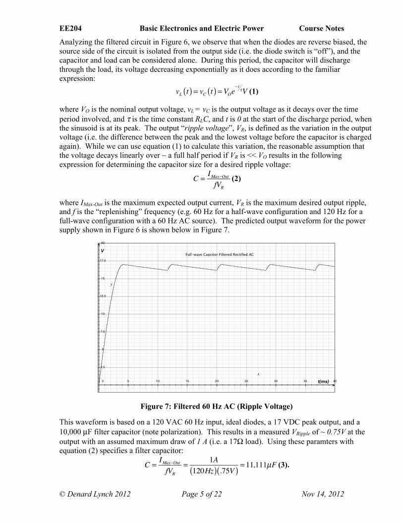
Analyzing the filtered circuit in Figure 6, we observe that when the diodes are reverse biased, the source side of the circuit is isolated from the output side (i.e. the diode switch is “off”), and the capacitor and load can be considered alone. During this period, the capacitor will discharge through the load, its voltage decreasing exponentially as it does according to the familiar expression:
vL t( ) = vC t( ) =VOe− t
τV (1)
where VO is the nominal output voltage, vL = vC is the output voltage as it decays over the time period involved, and τ is the time constant RLC, and t is 0 at the start of the discharge period, when the sinusoid is at its peak. The output “ripple voltage”, VR, is defined as the variation in the output voltage (i.e. the difference between the peak and the lowest voltage before the capacitor is charged again). While we can use equation (1) to calculate this variation, the reasonable assumption that the voltage decays linearly over ~ a full half period if VR is << VO results in the following expression for determining the capacitor size for a desired ripple voltage:
C = IMax−OutfVR
(2)
where IMax-Out is the maximum expected output current, VR is the maximum desired output ripple, and f is the “replenishing” frequency (e.g. 60 Hz for a half-wave configuration and 120 Hz for a full-wave configuration with a 60 Hz AC source). The predicted output waveform for the power supply shown in Figure 6 is shown below in Figure 7.
Figure 7: Filtered 60 Hz AC (Ripple Voltage)
This waveform is based on a 120 VAC 60 Hz input, ideal diodes, a 17 VDC peak output, and a 10,000 µF filter capacitor (note polarization). This results in a measured VRipple of ~ 0.75V at the output with an assumed maximum draw of 1 A (i.e. a 17Ω load). Using these paramters with equation (2) specifies a filter capacitor:
C = IMax−OutfVR
= 1A120Hz( ) .75V( ) = 11,111µF (3).
0 5 10 15 20 25 30 35 40
2.5
5
7.5
10
12.5
15
17.5
20
V
t(ms)
Full-wave Capcitor Filtered Rectified AC

EE204 Basic Electronics and Electric Power Course Notes
© Denard Lynch 2012 Page 6 of 22 Nov 14, 2012
Note that this is both reasonably close and errs on the “safe” side of the actual 10,000µF capacitor actually used in the plot calculation. This small “safety margin” will help compensate for component variation (a 10% tolerance in value is not uncommon) and ensure the desired specification are met or exceeded. The “charge” and “discharge” cycle occur over a half cycle of the input frequency, or 8.333 ms in this case. Observe that the waveform during the latter half of this period could be accurately represented by the expression -VPeakcos(ωt). Equating this with the exponential expression for the decaying voltage across the capacitor (starting with t=0 at one peak) and solving for t would find the time when the rising source voltage (load side of diode) would be equal to the exponentially decaying output voltage. This would let us separate the period in to the charge and discharge portions, as labelled in Figure 8. An algebraic solution to this equation is illusive, but if the peak output voltage, the frequency of the source and the size of the filter capacitor are know, a graphical solution can be obtained. If, for example, we use the previous example parameters (60 Hz, full wave rectified source, peak output voltage of 17V, a 1 Ampere draw at peak voltage (17Ω load), and a 10µF capacitor) the associated decay (discharge) time is ~ 7.5 ms. This leaves 0.833 ms to replenish the charge lost from the capacitor and bring vC back to the peak output voltage. This information can be used to estimate the average and peak current capability of the diodes.
Figure 8: Filtered 60 Hz AC (10µF Capacitor)
Since the amount of charge lost from the capacitor during the discharge portion of this cycle must be replenished during the charge portion, the “time-current” integral (Q = I ⋅ t ) must be the same in each part of the cycle. Again, the reasonable assumption that VR << VO simplifies analysis. In the example used here, 1 A is being drawn for 7.5 ms. so 1A( ) 7.5ms .8333ms( ) = 9A plus the 1A also
drawn by the load during this period = 10 A that must pass though the diode during the “charging”
portion of this cycle. The average is .8338.33
10A = 1A. Observe that the smaller the proportion of
time available to “re-charge” the capacitor, the higher the ratio between the peak current and the average current.
0 1 2 3 4 5 6 7 8 9 10 11 12 13 14 15
11
12
13
14
15
16
17
18
19
20
V
t(ms)
Full-wave Capcitor Filtered Rectified AC
charge time
discharge time
V ripple
EE204 Basic Electronics and Electric Power Course Notes
© Denard Lynch 2012 Page 7 of 22 Nov 14, 2012
This relationship can be manipulated into the more general expression:
IPeak = IOut−Max 1+tdischargetcharge
⎛
⎝⎜⎞
⎠⎟(4)
where IPeak is the peak diode current required, IOut-Max is the maximum output current ca[ability required of the supply, and tdischarge and tcharge must be determined graphically or by linear estimation. The key parameters of a mains-fed power supply of the type described above are summarized in Table 1.
Table 1: Key Power Supply Characteristics
Characteristic Description VO The desired output voltage for the supply IO The maximum output current required VR The maximum allowed output voltage variation at the maximum output
current Cf The size of filter capacitor required to achieve the desired VR. It must also
have a voltage rating of at least VO ID The peak forward current rating for the rectifier diodes. Determine charge
times using the filter capacitor size to estimate charge time, and equation 4). The average current requirement is equal to the maximum output current, IO.
Completing the example design used above will also demonstrate the process of ensuring a reliable and capable power supply.

EE204 Basic Electronics and Electric Power Course Notes
© Denard Lynch 2012 Page 8 of 22 Nov 14, 2012
Power Supply Example 1: Determine the parameters for an off-line (120VAC source) 12VDC, 3A power supply with a maximum ripple voltage of 2%. Use a step-down transformer to design an unregulated “raw” supply with these specifications. Expanding a bit on the parameters: 2% ripple is .24V or ±.12 volts, so the output can vary (ripple) from 11.88 to 12.12V. We have 3 common choices for configuration: ½ wave, full-wave and full-wave bridge. Since we are short of diodes and would like to keep the filter capacitor as small as possible, let’s choose a full wave with a centre-tapped secondary transformer (only 2 diodes required for full-wave). Typical silicon power diodes have a conducting threshold of ~0.7 volts, and a VF of ~1.1V at 3A (1N4007 datasheet). We should design for worst case, so we need another 1.1 volts peak from the transformer so we have 12.12 at the output. The RMS voltage we need out of the transformer is
12.12V +1.1V2
= 9.35VRMS
Transformers are usually spec’d with an output voltage in RMS at a specified secondary current. Looking at the table in Figure 10 (Signal Transformer), we find model 14A - 56 – 20 with a CT secondary of 20VRMS ( 10V each side of centre) at a current of 2.8A. This isn’t enough and we should continue the search, but for
now we’ll assume we can find one similar, spec’d at 3A secondary. (Actually, to get a 3A average secondary current, we need and RMS current of 3.33A (3A average means:
3A2π= 4.71APeak =
4.17APeak2
= 3.33ARMS .)
This model will give us an extra .65VRMS which may be helpful to overcome unforeseen losses. The next step is to calculate the size of the filter capacitor. With the familiar configuration shown in Figure 11, we can use the commonly accepted expression:
CF =IOutfVRipple
(5)
CF is the size of the filter capacitor in Farads, IOut is the maximum average output current, f is the frequency of the “re-charging” (e.g. for a full wave rectified 60 Hz source, the capacitor is “re-charged”
Figure 9: 1N4007 VF Characteristic
Figure 10: Type 14A Transformer Table

EE204 Basic Electronics and Electric Power Course Notes
© Denard Lynch 2012 Page 9 of 22 Nov 14, 2012
120/s, so F = 120), and VRipple is the maximum desired (peak-to-peak) variation in the output voltage.
Figure 11: Full-wave Centre-tap configuration
For your design we have:
CF =IOutfVRipple
= 3A120( ) .24V( ) = 104,170µF
Of course we will probably have to use the next higher commercially available size. Find the peak current rating for the diodes: Our average current rating for the rectifier diodes is 3A, as implied by the output parameter. To determine the peak current, we must somehow estimate the ratio of the “discharge” time to the
“charge” time, and we can then use the equation: IPeak = IOut−Max 1+tdischargetcharge
⎛
⎝⎜⎞
⎠⎟(4)
What we need to do this is to find the time at which the decaying capacitor voltage intersects the rectified sinusoid that will re-charge it. One way to get a reasonable estimate is to simplify the discharge curve and assume it will reach the maximum discharge by the time the sinusoid intersects (refer again to Figure 8). Then the discharge time will be when the sinusoid reaches VPeak – VRipple. If we “re-start the clock” at the beginning of the rising sinusoid, we can use the expression v(t) = VPsin(ωt) = VPeak – VRipple to describe the waveform in that period. We must add to that ¼ of the period of the source waveform (60 Hz in this case, not the 120 Hz we used in the capacitor calculation). The total discharge time is then:
tdis =14 f
+sin−1 VP −VR
VP( )3600( ) f( )
(6)
Using our values:
tdis =1
4 60( ) +sin−1 12.12 − .24
12.12( )3600( ) 60( ) = 7.805ms , and:
tdistchg
= tdis12 f − tdis( ) =
7.805ms8.333ms − 7.805ms( ) = 14.8
Our peak current is then (3A)(14.8) = 44.35A
120:24
.
.
..
.
TR12
4
1
5
3 C1
LOAD
AC1
AC2

EE204 Basic Electronics and Electric Power Course Notes
© Denard Lynch 2012 Page 10 of 22 Nov 14, 2012
In summary (Table 2), we would need components with the following spec’s: Table 2: Power Supply Component Summary
Component Description Transformer 120VAC primary with 18.7VAC CT secondary (9.35V per half) @3.33A Diodes (1) IAvg=3A; I)=45A
PIV (peak inverse voltage): 9.35 2 V (more if we have to pick a transformer with a slightly higher secondary voltage
Capacitor 105,000µF; 12.2WVDC (working volts DC), higher if we account for the probably higher no-load voltage coming from the transformer secondary. E/g/ if the internal resistance was .4Ω, we would have another 1.2V peak at no load compared to 3A. If spec’s are not available for this parameter, it may have to be measured or estimated. In this size range, electrolytics are the only reasonable economic choice today. These are polarized, and should never be subjected to a reverse voltage.
EE204 Basic Electronics and Electric Power Course Notes
© Denard Lynch 2012 Page 11 of 22 Nov 14, 2012
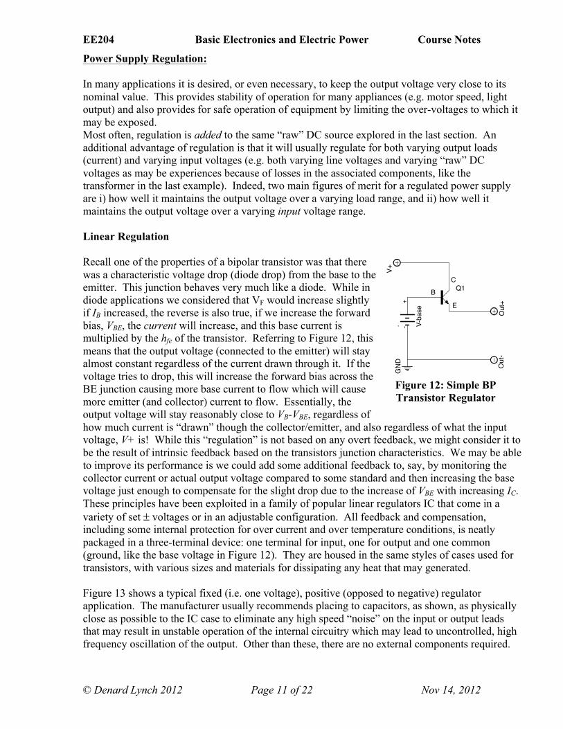
Power Supply Regulation: In many applications it is desired, or even necessary, to keep the output voltage very close to its nominal value. This provides stability of operation for many appliances (e.g. motor speed, light output) and also provides for safe operation of equipment by limiting the over-voltages to which it may be exposed. Most often, regulation is added to the same “raw” DC source explored in the last section. An additional advantage of regulation is that it will usually regulate for both varying output loads (current) and varying input voltages (e.g. both varying line voltages and varying “raw” DC voltages as may be experiences because of losses in the associated components, like the transformer in the last example). Indeed, two main figures of merit for a regulated power supply are i) how well it maintains the output voltage over a varying load range, and ii) how well it maintains the output voltage over a varying input voltage range. Linear Regulation Recall one of the properties of a bipolar transistor was that there was a characteristic voltage drop (diode drop) from the base to the emitter. This junction behaves very much like a diode. While in diode applications we considered that VF would increase slightly if IB increased, the reverse is also true, if we increase the forward bias, VBE, the current will increase, and this base current is multiplied by the hfe of the transistor. Referring to Figure 12, this means that the output voltage (connected to the emitter) will stay almost constant regardless of the current drawn through it. If the voltage tries to drop, this will increase the forward bias across the BE junction causing more base current to flow which will cause more emitter (and collector) current to flow. Essentially, the output voltage will stay reasonably close to VB-VBE, regardless of how much current is “drawn” though the collector/emitter, and also regardless of what the input voltage, V+ is! While this “regulation” is not based on any overt feedback, we might consider it to be the result of intrinsic feedback based on the transistors junction characteristics. We may be able to improve its performance is we could add some additional feedback to, say, by monitoring the collector current or actual output voltage compared to some standard and then increasing the base voltage just enough to compensate for the slight drop due to the increase of VBE with increasing IC. These principles have been exploited in a family of popular linear regulators IC that come in a variety of set ± voltages or in an adjustable configuration. All feedback and compensation, including some internal protection for over current and over temperature conditions, is neatly packaged in a three-terminal device: one terminal for input, one for output and one common (ground, like the base voltage in Figure 12). They are housed in the same styles of cases used for transistors, with various sizes and materials for dissipating any heat that may generated. Figure 13 shows a typical fixed (i.e. one voltage), positive (opposed to negative) regulator application. The manufacturer usually recommends placing to capacitors, as shown, as physically close as possible to the IC case to eliminate any high speed “noise” on the input or output leads that may result in unstable operation of the internal circuitry which may lead to uncontrolled, high frequency oscillation of the output. Other than these, there are no external components required.
Figure 12: Simple BP Transistor Regulator
V-base Out+
Out-
V+GND
Q1
.+
-
BC
E

EE204 Basic Electronics and Electric Power Course Notes
© Denard Lynch 2012 Page 12 of 22 Nov 14, 2012
Figure 13: IC Voltage Regulator
The optional resistor shown in the schematic is to reduce the dissipation demands on the regulator itself. A simple power analysis will determine the dissipation requirements for the device itself. If, for example, the regulator is capable of delivering 1A at 5VDC output, and the input voltage is 20VDC on average, there is (20V)(1A)=20W going into the device and (5VDC)(1A) coming out, the difference, 15W, must be dissipated in the device itself! This can lead to high temperatures in the device and surrounding enclosure which could damage the dive if not removed effectively. In situations where there is a significant voltage difference between the input and output voltage, we can remove some of the power dissipation from the device by lowering the voltage by using a dropping resistor. This technique will be demonstrated in a subsequent example. The key characteristics and parameters of such linear regulators are summarized in Table 3.
Table 3: Summary of Linear Regulator Characteristics
Characteristic Description VO Same as any power supply: the specified nominal output voltage IO The maximum specified output current capability
Drop Out voltage The minimum difference between Vin and Vout. As with Op Amps, there is some “circuit overhead” that requires some voltage in excess of the output voltage.
Maximum Input Voltage The maximum input voltage allowed for safe operation Line regulation How much the output voltage varies with a change in input voltage
Load Regulation How much the output voltage varies with a change in output current (usually specified over most of the maximum current range)
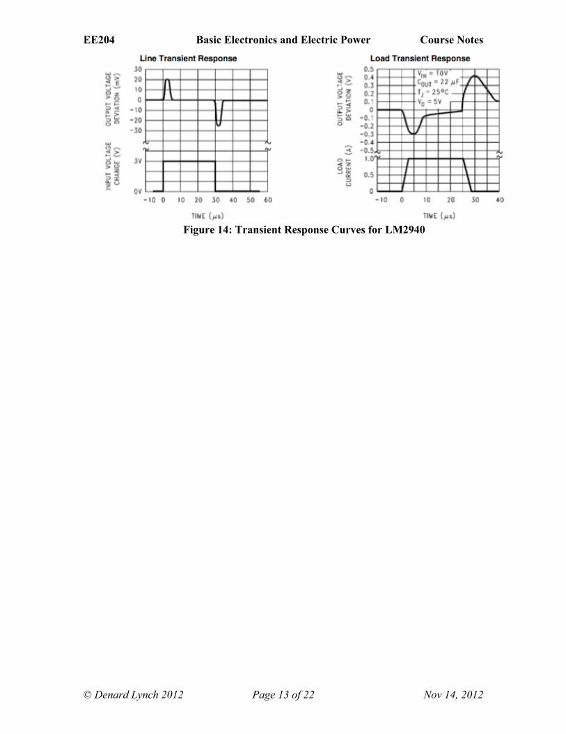
Line Transient Response How the output voltage varies in response to abrupt changes in the input voltage (see Figure 14)
Load Transient Response How the output voltage varies in response to abrupt changes in load current (see Figure 14)
Out
+O
ut-
V+ In
GNDV-
In
+ RegulatorIC1
GNDVI1
2
VO 3
C1 C2
R1Optional
EE204 Basic Electronics and Electric Power Course Notes
© Denard Lynch 2012 Page 13 of 22 Nov 14, 2012
Figure 14: Transient Response Curves for LM2940
EE204 Basic Electronics and Electric Power Course Notes
© Denard Lynch 2012 Page 14 of 22 Nov 14, 2012
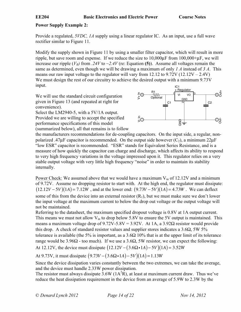
Power Supply Example 2: Provide a regulated, 5VDC, 1A supply using a linear regulator IC. As an input, use a full wave rectifier similar to Figure 11. Modify the supply shown in Figure 11 by using a smaller filter capacitor, which will result in more ripple, but save room and expense. If we reduce the size to 10,000µF from 100,000+µF, we will increase our ripple (VR) from .24V to ~2.4V (re: Equation (5)). Assume all voltages remain the same as determined, even though we will be drawing a maximum of only 1 A instead of 3 A. This means our raw input voltage to the regulator will vary from 12.12 to 9.72V (12.12V – 2.4V) We must design the rest of our circuitry to achieve the desired output with a minimum 9.73V input. We will use the standard circuit configuration given in Figure 13 (and repeated at right for convenience). Select the LM2940-5, with a 5V/1A output. Provided we are willing to accept the specified performance specifications of this model (summarized below), all that remains is to follow the manufacturers recommendations for de-coupling capacitors. On the input side, a regular, non-polarized .47µF capacitor is recommended. On the output side however (C2), a minimum 22µF “low ESR” capacitor is recommended. “ESR” stands for Equivalent Series Resistance, and is a measure of how quickly the capacitor can charge and discharge, which affects its ability to respond to very high frequency variations in the voltage impressed upon it. This regulator relies on a very stable output voltage with very little high frequency “noise” in order to maintain its stability internally. Power Check: We assumed above that we would have a maximum Vin of 12.12V and a minimum of 9.72V. Assume no dropping resistor to start with. At the high end, the regulator must dissipate: 12.12V − 5V( ) 1A( ) = 7.12W , and at the lower end: 9.73V − 5V( ) 1A( ) = 4.73W . We can deflect
some of this from the device into an external resistor (R1), but we must make sure we don’t lower the input voltage at the maximum current to below the drop out voltage or the output voltage will not be maintained. Referring to the datasheet, the maximum specified dropout voltage is 0.8V at 1A output current. This means we must not allow Vin to drop below 5.8V to ensure the 5V output is maintained. This means a maximum voltage drop of 9.72V-5.8V = 3.92V. At 1A, a 3.92Ω resistor would provide this drop. A check of standard resistor values and supplier stores indicates a 3.6Ω, 5W 5% tolerance is available (the 5% is important, as a 3.6Ω 10% that is at the upper limit of its tolerance range would be 3.96Ω - too much). If we use a 3.6Ω, 5W resistor, we can expect the following: At 12.12V, the device must dissipate 12.12V − 3.6Ω i1A( )− 5V( ) 1A( ) = 3.52W
At 9.73V, it must dissipate 9.73V − 3.6Ω i1A( )− 5V( ) 1A( ) = 1.13W Since the device dissipation varies constantly between the two extremes, we can take the average, and the device must handle 2.33W power dissipation. The resistor must always dissipate 3.6W (1A2R), at least at maximum current draw. Thus we’ve reduce the heat dissipation requirement in the device from an average of 5.9W to 2.3W by the
Out
+O
ut-
V+ In
GNDV-
In
+ RegulatorIC1
GNDVI1
2
VO 3
C1 C2
R1Optional

EE204 Basic Electronics and Electric Power Course Notes
© Denard Lynch 2012 Page 15 of 22 Nov 14, 2012
addition of an additional external component. It may also be easier to physically place the resistor away from the other circuitry for cooling. The specifications are now dependent on the IC’s spec’s:
• Maximum input voltage: 26V • Output voltage: 4.85 – 5.15V (device variation) • Line regulation: 50mV (Vin +2 to 26V • Load Regulation: 50mV (IO 50mA to 1A)
EE204 Basic Electronics and Electric Power Course Notes
© Denard Lynch 2012 Page 16 of 22 Nov 14, 2012
Regulated Switch-Mode Power Supplies In a previous section, we noted one of the disadvantages of linear power supply regulation was the inefficiency (wasted energy). Switch-Mode Power Supplies (SMPS) exploit some of the characteristics of inductors and transformers to realize a more efficient, flexible design. Improvements in solid-state devices (like transistors and diodes) have made SMPS the common design choice for almost all conversion applications. This section discusses the basic principle of operation and the key characteristics of SMPSs. Operating Principle Recall that capacitors and inductors temporarily store energy in another form (and electric field in a capacitor, and a magnetic field in an inductor). While either could in theory be used, the inductor proves to be advantageous because of its ability to “self generate” any required voltage to “discharge” the energy stored in its magnetic field. Typically use a small, light inductor is used, exploiting the relationship between frequency, flux and voltage represented by:
EP−max = 2π fN pΦmax (7).
Note that as f increases, N and Φ (related to inductance) will decrease for a given energy transfer rate (power). Regulating the output is typically achieved by varying the amount of energy “loaded” into the magnetic field in order to accommodate variations in the input supply or the output load. By designing suitable circuitry, we are able to extract energy from a source with one voltage, temporarily store it in a magnetic field, and then “discharge” it at another voltage into a load. Unlike the linear power supplies considered previously, SMPSs also have the advantage that the only losses in the voltage “conversion” process are the relatively minor component losses (e.g. core losses in the inductor), which can be kept very low leading to very high efficiencies. SMPSs can have a variety of configurations, but they may be categorized as one of two basic types: the flyback or buck-boost converter, and the forward or buck converter. A third common designation is the push-pull converter, which is a variation of the forward converter. These all exploit the same principles, but vary in how the components are arranged depending on whether the desired output voltage is higher or lower than the source voltage. Exploring the operation of one configuration, the flyback converter, will adequately demonstrate the basic principles of operation which apply to other configurations as well. Flyback Converters: (Lynch) A flyback converter is a fairly simple architecture that is easy to construct and manipulate. To understand the basic design, considering the inductor storage element is a good starting point. You may recall that the energy stored in an inductor is:
W = LI 2
2, (8)
and that the voltage across an inductor is:
vL = Ldidt
. (9)
EE204 Basic Electronics and Electric Power Course Notes
© Denard Lynch 2012 Page 17 of 22 Nov 14, 2012
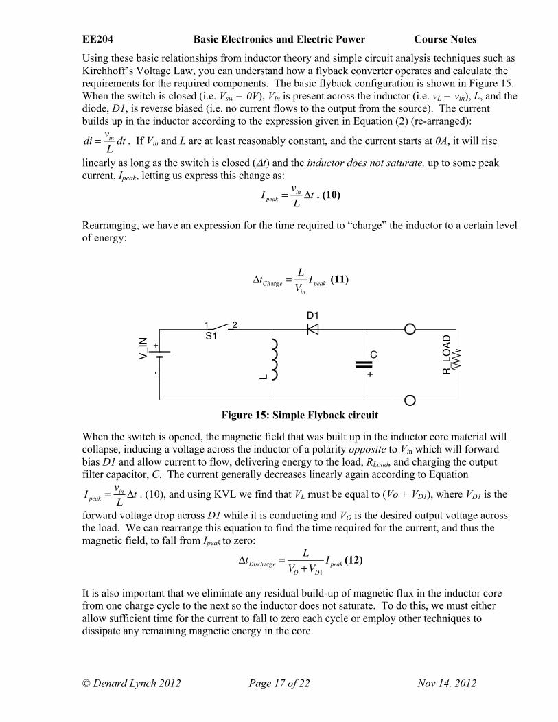
Using these basic relationships from inductor theory and simple circuit analysis techniques such as Kirchhoff’s Voltage Law, you can understand how a flyback converter operates and calculate the requirements for the required components. The basic flyback configuration is shown in Figure 15. When the switch is closed (i.e. Vsw = 0V), Vin is present across the inductor (i.e. vL = vin), L, and the diode, D1, is reverse biased (i.e. no current flows to the output from the source). The current builds up in the inductor according to the expression given in Equation (2) (re-arranged):
di = vinLdt . If Vin and L are at least reasonably constant, and the current starts at 0A, it will rise
linearly as long as the switch is closed (Δt) and the inductor does not saturate, up to some peak current, Ipeak, letting us express this change as:
I peak =vinLΔt . (10)
Rearranging, we have an expression for the time required to “charge” the inductor to a certain level of energy:
ΔtCharge =LVin
I peak (11)
Figure 15: Simple Flyback circuit
When the switch is opened, the magnetic field that was built up in the inductor core material will collapse, inducing a voltage across the inductor of a polarity opposite to Vin which will forward bias D1 and allow current to flow, delivering energy to the load, RLoad, and charging the output filter capacitor, C. The current generally decreases linearly again according to Equation
I peak =vinLΔt . (10), and using KVL we find that VL must be equal to (Vo + VD1), where VD1 is the
forward voltage drop across D1 while it is conducting and VO is the desired output voltage across the load. We can rearrange this equation to find the time required for the current, and thus the magnetic field, to fall from Ipeak to zero:
ΔtDischarge =L
VO +VD1I peak (12)
It is also important that we eliminate any residual build-up of magnetic flux in the inductor core from one charge cycle to the next so the inductor does not saturate. To do this, we must either allow sufficient time for the current to fall to zero each cycle or employ other techniques to dissipate any remaining magnetic energy in the core.
V_IN +
-
C
S11 2
L R_LO
AD
D1
+

EE204 Basic Electronics and Electric Power Course Notes
© Denard Lynch 2012 Page 18 of 22 Nov 14, 2012
If we make the simplifying assumption that VD1 is negligible compared to VO, we can re-arrange equations (10) and (11) to get an expression for the duty cycle (the ratio of the charge time to the total time):
γ =tCharge
tCharge + tDischarge= 1
1+ VinVout
(13)
Recall from equation (10) that the energy that can be stored in the inductor, (and thus transferred to the load during one “cycle”) is a function of the time the inductor is “charged”, and from equation (12) we note that the charge time is a function of the ratio of Vin to Vout. This is an unwanted limitation of this simple configuration. The advantage of the flyback configuration is that the full input voltage, Vin, can be used to “charge” the inductor, regardless of the output voltage, and the inductor will generate what ever voltage is require to discharge this energy when the field collapses. Thus, the output voltage, Vo, may be either lower (buck, or step-down) or higher (boost, or step-up) than Vin. The amount of charge put into C will depend in the energy that was stored in the inductor (given in Equation (1)), which is proportional to Ipeak which in turn is dependent on the length of time the switch was closed, Δt. By adjusting the length of time or how often the switch is closed, we can provide just enough energy to the output capacitor to make up for the current that was drawn by whatever load, RL, we might attach to the output. Of course, between charges the voltage across the capacitor will decrease, giving Vo a “ripple”, similar to the conventional full-wave rectifiers studied previously. The amount of ripple will depend on the size of C, the load current, and how often the energy is “replenished”. A distinct advantage of a SMPS is that the frequency can by made very high, since it can be controlled by the circuitry, and not limited to the power line frequency. This means the size of capacitor required for a given VRipple is very small compared to a 60 Hz line-fed supply, and the inductor can also be very small as only a very small amount of energy needs to be transferred each cycle as long as the “cycle rate” is very high. There are two other considerations with the simple configuration shown in Figure 15. First, there is no electrical isolation between the input and output. When dealing with off-line power supplies (i.e. directly connected to a commercial AC power source), Vin could easily be several hundred volts, which presents a safety hazard. The second issue is that Vo is inverted with respect to Vin, which will make it much more complicated to monitor Vo and adjust the parameters of the “charge” cycle and regulate the output voltage accordingly. Figure 16, also shows a simple version of the flyback configuration that uses a transformer as the inductance, which addresses both of these problems. The operation is identical except that the energy built up by current in the primary when the switch is turned on is recovered through current flowing in the secondary when the switch is turned off. The currents and voltages, as you will recall, are related by the turns ratio of the transformer. If we modify Vin and Vout in equation (13) with the transformer turns ratio, this also provides the advantage of allowing approximately half the total cycle for each of the charge time and discharge time thus optimizing the energy transfer for a given inductance. The other “improvement” made in Figure 16 is that a FET is used as a switch and put in the “ground” side of the circuit. This facilitates turning the “switch” on and off very quickly with an electric signal. You can also see that, because the secondary is electrically isolated, we are no longer faced with the same safety hazard, and the negative side can potentially be connected to the same signal ground as the switch control circuitry making it easier to use feedback from the output

EE204 Basic Electronics and Electric Power Course Notes
© Denard Lynch 2012 Page 19 of 22 Nov 14, 2012
to control the switch (In practice, an opto-isolator is often used to provide additional isolation between the output and input, especially when the control circuitry is powered from Vin.) A simple feedback loop is also shown to illustrate the basic mechanism typically used to control the output voltage.
Figure 16: Transformer-based Flyback Configuration
Figure 17 shows a summary of the voltages and current across the main components during one “cycle”. The voltage across the primary (i.e. inductance) can be obtained by applying KVL while the switch is closed, and then open. A similar analysis gives the voltage across the switch, which is a key consideration when specifying the FET parameters. The peak primary current is also needed to determine the FET switch requirements, and the peak output current is needed to specify the required diode characteristics. Not shown is the peak inverse voltage (PIV) across the diode, which could also be obtained applying KVL during the “charge” part of the cycle when it is reverse biased and not conducting. Key Characteristics Most of the characteristics that apply to other power supplies also apply to SMPSs, namely input and output voltage, power handling capability (i.e. output current), and both static and dynamic line and load regulation, In addition, because of the high frequencies involved, the electromagnetic fields generated have the possibility of causing electromagnetic interference (EMI). While this is not generally considered a “power supply” specifications, it may be of concern if the supply is to operate in the vicinity of other equipment that may be adversely affected by EMI.
V_IN +
-C
R_LO
AD
TR1
FET
SW
D1
G
D
S
V_outFeedbackControl
VPri
Vin+Vout+VD1
Vin
Iout-peak
Iin-peak
-(Vout+VD1)/n
Vin
Iin
Iout
VSw
Figure 17: SMPS Voltages and Currents
EE204 Basic Electronics and Electric Power Course Notes
© Denard Lynch 2012 Page 20 of 22 Nov 14, 2012
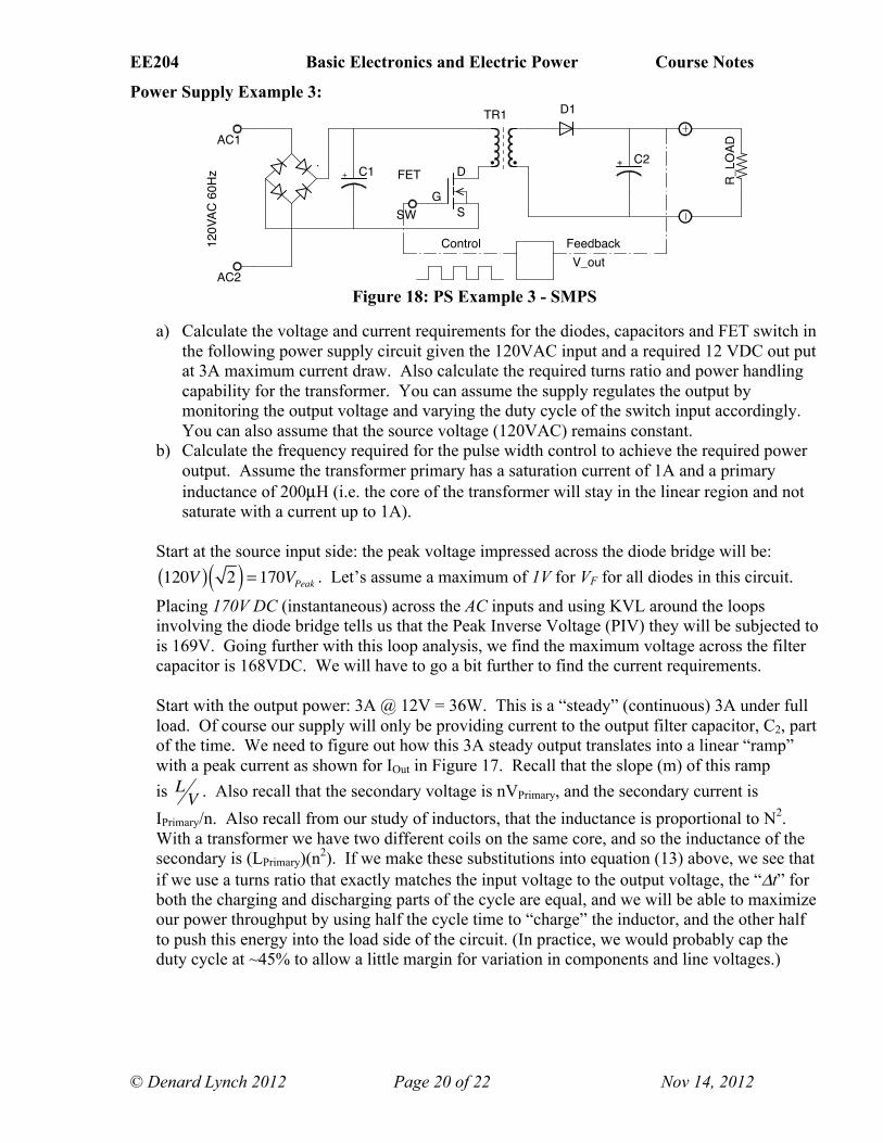
Power Supply Example 3:
Figure 18: PS Example 3 - SMPS
a) Calculate the voltage and current requirements for the diodes, capacitors and FET switch in the following power supply circuit given the 120VAC input and a required 12 VDC out put at 3A maximum current draw. Also calculate the required turns ratio and power handling capability for the transformer. You can assume the supply regulates the output by monitoring the output voltage and varying the duty cycle of the switch input accordingly. You can also assume that the source voltage (120VAC) remains constant.
b) Calculate the frequency required for the pulse width control to achieve the required power output. Assume the transformer primary has a saturation current of 1A and a primary inductance of 200µH (i.e. the core of the transformer will stay in the linear region and not saturate with a current up to 1A).
Start at the source input side: the peak voltage impressed across the diode bridge will be: 120V( ) 2( ) = 170VPeak . Let’s assume a maximum of 1V for VF for all diodes in this circuit.
Placing 170V DC (instantaneous) across the AC inputs and using KVL around the loops involving the diode bridge tells us that the Peak Inverse Voltage (PIV) they will be subjected to is 169V. Going further with this loop analysis, we find the maximum voltage across the filter capacitor is 168VDC. We will have to go a bit further to find the current requirements. Start with the output power: 3A @ 12V = 36W. This is a “steady” (continuous) 3A under full load. Of course our supply will only be providing current to the output filter capacitor, C2, part of the time. We need to figure out how this 3A steady output translates into a linear “ramp” with a peak current as shown for IOut in Figure 17. Recall that the slope (m) of this ramp is LV . Also recall that the secondary voltage is nVPrimary, and the secondary current is IPrimary/n. Also recall from our study of inductors, that the inductance is proportional to N2. With a transformer we have two different coils on the same core, and so the inductance of the secondary is (LPrimary)(n2). If we make these substitutions into equation (13) above, we see that if we use a turns ratio that exactly matches the input voltage to the output voltage, the “Δt” for both the charging and discharging parts of the cycle are equal, and we will be able to maximize our power throughput by using half the cycle time to “charge” the inductor, and the other half to push this energy into the load side of the circuit. (In practice, we would probably cap the duty cycle at ~45% to allow a little margin for variation in components and line voltages.)
R_LO
AD
TR1
FET
SW
.C1
C2AC1
AC2
D1
G
D
S
V_outFeedbackControl12
0VAC
60H
z
EE204 Basic Electronics and Electric Power Course Notes
© Denard Lynch 2012 Page 21 of 22 Nov 14, 2012
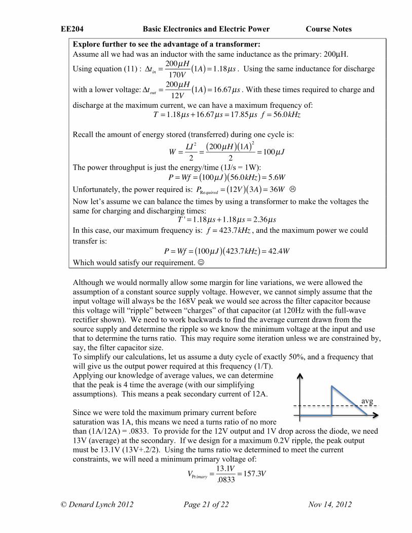
Explore further to see the advantage of a transformer: Assume all we had was an inductor with the same inductance as the primary: 200µH.
Using equation (11) : Δtin =200µH170V
1A( ) = 1.18µs . Using the same inductance for discharge
with a lower voltage:Δtout =200µH12V
1A( ) = 16.67µs . With these times required to charge and
discharge at the maximum current, we can have a maximum frequency of: T = 1.18µs +16.67µs = 17.85µs f = 56.0kHz
Recall the amount of energy stored (transferred) during one cycle is:
W = LI 2
2=200µH( ) 1A( )2
2= 100µJ
The power throughput is just the energy/time (1J/s = 1W): P =Wf = 100µJ( ) 56.0kHz( ) = 5.6W
Unfortunately, the power required is: PRequired = 12V( ) 3A( ) = 36W Now let’s assume we can balance the times by using a transformer to make the voltages the same for charging and discharging times:
T ' = 1.18µs +1.18µs = 2.36µs In this case, our maximum frequency is: f = 423.7kHz , and the maximum power we could transfer is:
P =Wf = 100µJ( ) 423.7kHz( ) = 42.4W Which would satisfy our requirement. Although we would normally allow some margin for line variations, we were allowed the assumption of a constant source supply voltage. However, we cannot simply assume that the input voltage will always be the 168V peak we would see across the filter capacitor because this voltage will “ripple” between “charges” of that capacitor (at 120Hz with the full-wave rectifier shown). We need to work backwards to find the average current drawn from the source supply and determine the ripple so we know the minimum voltage at the input and use that to determine the turns ratio. This may require some iteration unless we are constrained by, say, the filter capacitor size. To simplify our calculations, let us assume a duty cycle of exactly 50%, and a frequency that will give us the output power required at this frequency (1/T). Applying our knowledge of average values, we can determine that the peak is 4 time the average (with our simplifying assumptions). This means a peak secondary current of 12A. Since we were told the maximum primary current before saturation was 1A, this means we need a turns ratio of no more than (1A/12A) = .0833. To provide for the 12V output and 1V drop across the diode, we need 13V (average) at the secondary. If we design for a maximum 0.2V ripple, the peak output must be 13.1V (13V+.2/2). Using the turns ratio we determined to meet the current constraints, we will need a minimum primary voltage of:
VPr imary =13.1V.0833
= 157.3V
avg
EE204 Basic Electronics and Electric Power Course Notes
© Denard Lynch 2012 Page 22 of 22 Nov 14, 2012
Since we have a peak of 168V on the primary side, we can withstand a ripple of (168-157.3=10.7V. The average current on the primary side (similar to the secondary reasoning) is ¼ the peak, or 0.25A. We can use these values to calculate the required filter capacitor on the input side:
C1 =.25A
120Hz( ) 10.7V( ) = 194.7µF
We can use the minimum input voltage to find our “charge” time:
Δtin =200µH157.3V
1A( ) = 1.27µs , and f = 2 ×1.27µs( )−1 = 393.25kHz
(Δtchg is ½ the cycle, assuming ideal conditions, so T = 2Δt.) A check of our output power at a maximum input current (1A peak in the primary), minimum input voltage (157V) at the low end of the ripple.
P =Wf = 100µJ( ) 393.25kHz( ) = 39.3W Calculation of the output filter capacitor size will finish our calculations:
C2 =3A
393.25kHz( ) .2V( ) = 38.1µF
Note the relatively small size of both filter capacitors compared to an off-line” supply alone! Finally, again using KVL, we can determine the voltage requirements for the FET switch:
+Vin + (VO/n) –VDS = 0; +168V +13V/.0833 -VDS = 0; VDS = 324V In summary, the component specifications would be:
1. Transformer: Lpri=200µH; ISat=1A; n=.0833 2. Input filter cap: 195µF, 168VDC 3. Bridge diodes: 169VDC PIV, Iavg=.25A 4. Output filter cap: 40µF, 13VDC, Low ESR 5. Output diode: 26V PIV, Iavg=3A, IPeak=12A, fast switching type 6. FET, VDS=324VDC, IPeak=1A