ee178 lecture 5 caohuu sjsu / xilinx fall 2009. static timing analysis even though a digital circuit...
Post on 19-Dec-2015
215 views
TRANSCRIPT

EE178 Lecture 5
CaohuuSJSU / XilinxFall 2009
Static Timing Analysis
• Even though a digital circuit may be logicallycorrect, you need to know how it will performin its physical implementation.– To meet a performance specification.– To evaluate how your design operates.

Static Timing Analysis
• Items of interest for analysis include:– Requirements for input signals to the circuit.– Internal performance, maximum clock frequency.– Behavior of output signals from the circuit.
• If there are pre-determined timing requirementsand specifications, this information is importantto determine compliance.
• Also important just to document circuit behavior.
Static Timing Analysis
• To analyze the circuit behavior, you need to knowmany parameters of the components in the circuit.– Combinational logic propagation delays.– Signal propagation delays through wire.– Sequential logic input requirements and
output valid delays.
Combinational Logic
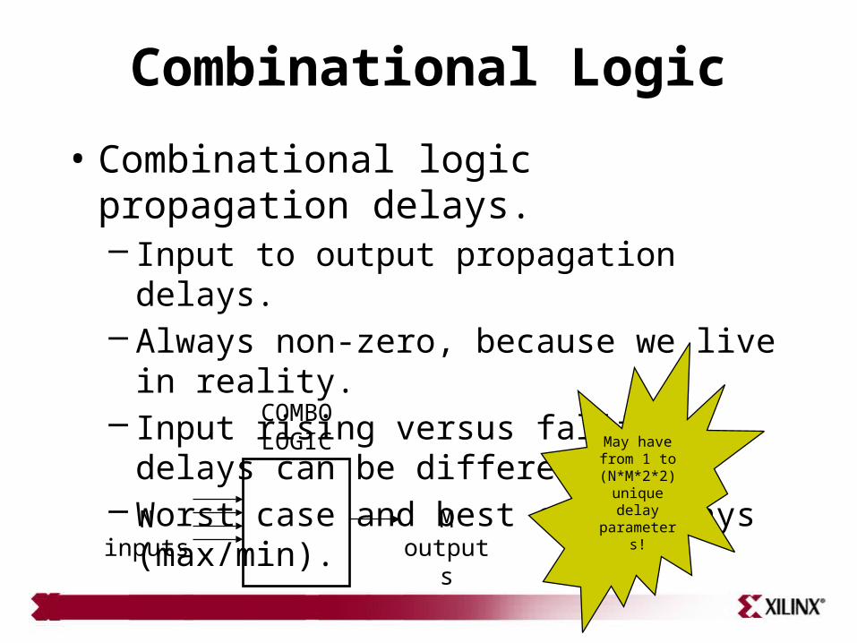
• Combinational logic propagation delays.– Input to output propagation delays.– Always non-zero, because we live in reality.– Input rising versus falling delays can be different.– Worst case and best case delays (max/min).
COMBOLOGIC
N inputs M outputs
May have from 1 to (N*M*2*2)
unique delay
parameters!

May have from 1 to 2
unique delay
parameters!
REALWIRE
1 input 1 output
Wires
• Signal propagation delays through wire.– Delays due to the physical nature of real wires
such as resistance, capacitance, inductance.– Always non-zero, because we live in reality.– Worst case and best case delays (max/min).
State Elements
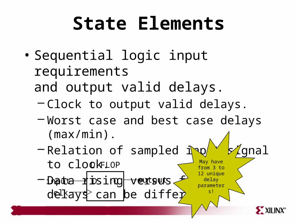
• Sequential logic input requirementsand output valid delays.– Clock to output valid delays.– Worst case and best case delays (max/min).– Relation of sampled input signal to clock.– Data rising versus falling delays can be different.
D FLOP
input outputD Qclk
May have from 3 to 12 unique
delay parameters
!
State Elements
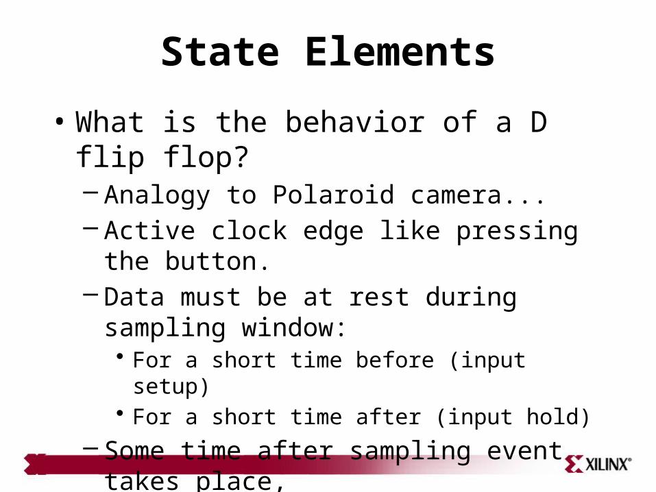
• What is the behavior of a D flip flop?– Analogy to Polaroid camera...– Active clock edge like pressing the button.– Data must be at rest during sampling window:
• For a short time before (input setup)• For a short time after (input hold)
– Some time after sampling event takes place,the sampled result is available (clock to out).
– Requirements must be observed for proper operation.
State Elements
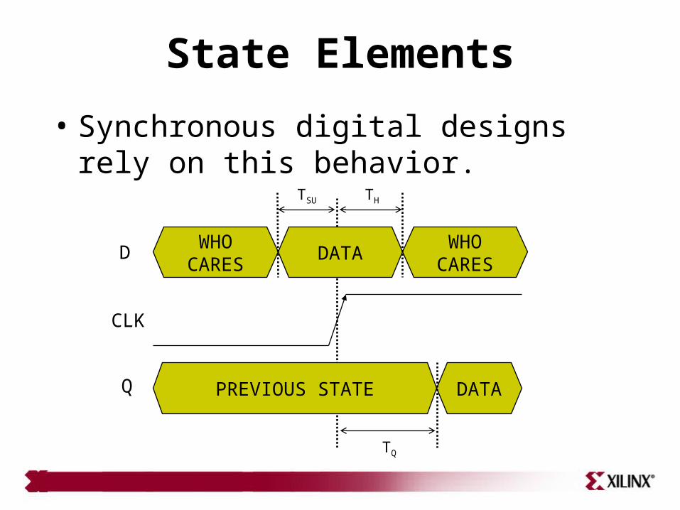
DATAWHO
CARESWHO
CARES
DATAPREVIOUS STATE
THTSU
TQ
Q
CLK
D
• Synchronous digital designs rely on this behavior.

State Elements
• If the flip flop input parameters are violated, thedevice may fail to correctly sample the input.
• Even worse, the flip flop may become metastable.– Observable as an increase in
the clock to out time.– The probability of remaining in
a metastable state decreasesexponentially with time.
• This causes synchronous digital designs to fail.
?
0 1
Sooner or later, but which way, and when?

State ElementsSubject: Thinking out loud about metastability...By: Philip Freidin
Flip flops may go metastable when input signals do notmeet the setup and hold specifications with regardto the clock signal. These inputs include D, CE, CLR,PRE, S, R, T, J, K.
There is no cure for metastability. What you can do is trade latency of your system for higher MTBF. People that have found a cure are wrong.
Circuits that purport to solve metastability through hysteresis fail because the hysteresis circuit itself can go metastable.
Circuits that purport to solve metastability with injected noise fail because the noise is as likely to push a non-metastable event into being a metastable event as it is to helping to resolve such an event.
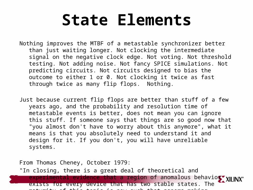
State ElementsNothing improves the MTBF of a metastable synchronizer better than just waiting longer. Not clocking the
intermediate signal on the negative clock edge. Not voting. Not threshold testing. Not adding noise. Not fancy SPICE simulations. Not predicting circuits. Not circuits designed to bias the outcome to either 1 or 0. Not clocking it twice as fast through twice as many flip flops. Nothing.
Just because current flip flops are better than stuff of a few years ago, and the probability and resolution time of metastable events is better, does not mean you can ignore this stuff. If someone says that things are so good now that "you almost don't have to worry about this anymore", what it means is that you absolutely need to understand it and design for it. If you don't, you will have unreliable systems.
From Thomas Cheney, October 1979:"In closing, there is a great deal of theoretical and experimental evidence that a region of anomalous
behavior exists for every device that has two stable states. The maturity of this topic is now such that papers making contrary claims without theoretical or experimental support should not be accepted for publication".
Real World Effects
• All parameters vary based on PVT whichstands for Process, Voltage, Temperature.– Higher voltage usually speeds things up.– Higher temperature usually slows things down.– Process variation is more difficult to quantify.
• Most datasheets specify maximum delays.• Typical delays are not useful during analysis.• More difficult to specify minimum delays.
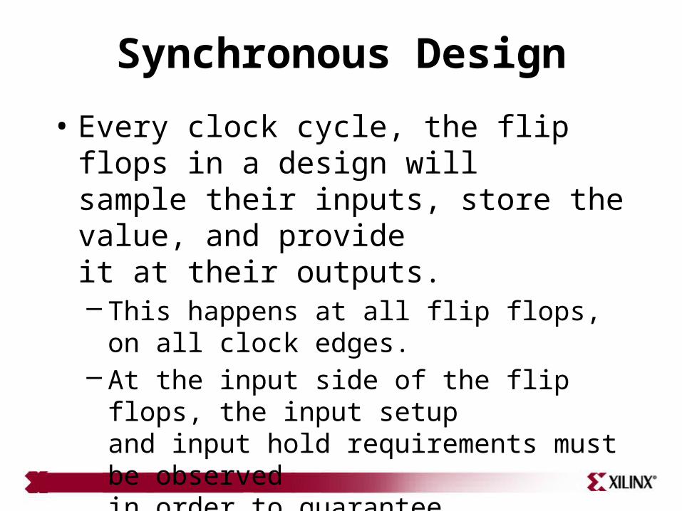
Synchronous Design
• Every clock cycle, the flip flops in a design willsample their inputs, store the value, and provideit at their outputs.– This happens at all flip flops, on all clock edges.– At the input side of the flip flops, the input setup
and input hold requirements must be observedin order to guarantee predictable behavior.
– This applies on-chip, and between chips, as longas they are synchronous -- a common clock.
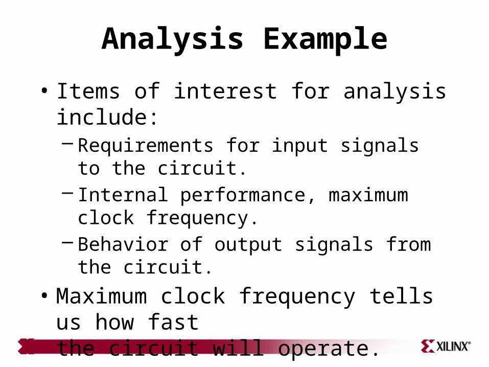
Analysis Example
• Items of interest for analysis include:– Requirements for input signals to the circuit.– Internal performance, maximum clock frequency.– Behavior of output signals from the circuit.
• Maximum clock frequency tells us how fastthe circuit will operate.
• Input and output behavior tells us how the circuitinteracts with other circuits and the outside world.
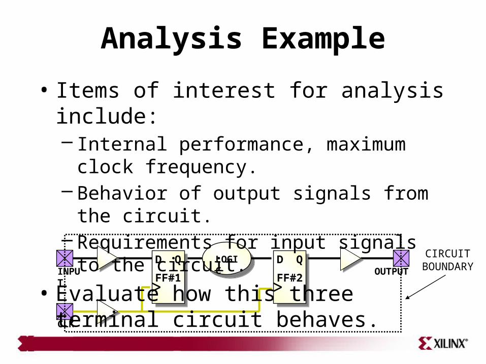
Analysis Example
CLK
OUTPUTD Q
FF#2
D Q
FF#1INPUT
LOGIC
• Items of interest for analysis include:– Internal performance, maximum clock frequency.– Behavior of output signals from the circuit.– Requirements for input signals to the circuit.
• Evaluate how this three terminal circuit behaves.
CIRCUITBOUNDAR
Y

Analysis Example
• Assume wire delays are TW = 0 ns.
• Buffers have delay of TB = 1 ns
• Logic has delay of TL = 7 ns
• Flip flops are identical with parameters:– Clock to out is TQ = 1 ns– Input setup is TSU = 2 ns– Input hold TH = 0 ns

Analysis Example
CLK
OUTPUTD Q
FF#2
D Q
FF#1INPUT
LOGIC
• Clock period behavior of circuit.– Clock event at FF#1 launches new data into logic.– Result sampled at FF#2 at next clock event.– Max delay sets min period = 1/(max frequency).– TQFF1 + TL + TSUFF2 = 10 ns min 100 MHz max
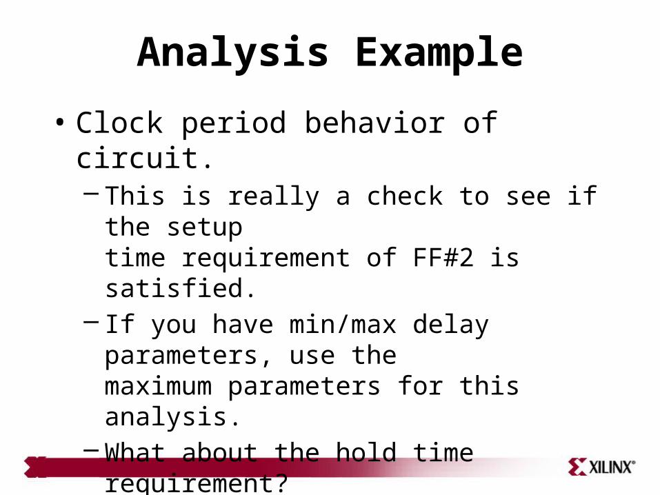
Analysis Example
• Clock period behavior of circuit.– This is really a check to see if the setup
time requirement of FF#2 is satisfied.– If you have min/max delay parameters, use the
maximum parameters for this analysis.– What about the hold time requirement?– Let’s check to see if it is satisfied...

Analysis Example
• Clock period behavior of circuit.– Clock event at FF#1 launches new data into logic.– Result must propagate slow enough to observe
hold time requirement at FF#2 for the old data.– TQFF1 + TL > THFF2 ?– If you have min/max delay parameters, use the
minimum parameters for this analysis.– If you design/use flip flops with guaranteed zero
hold time, this is always satisfied (no need to check).
Analysis Example
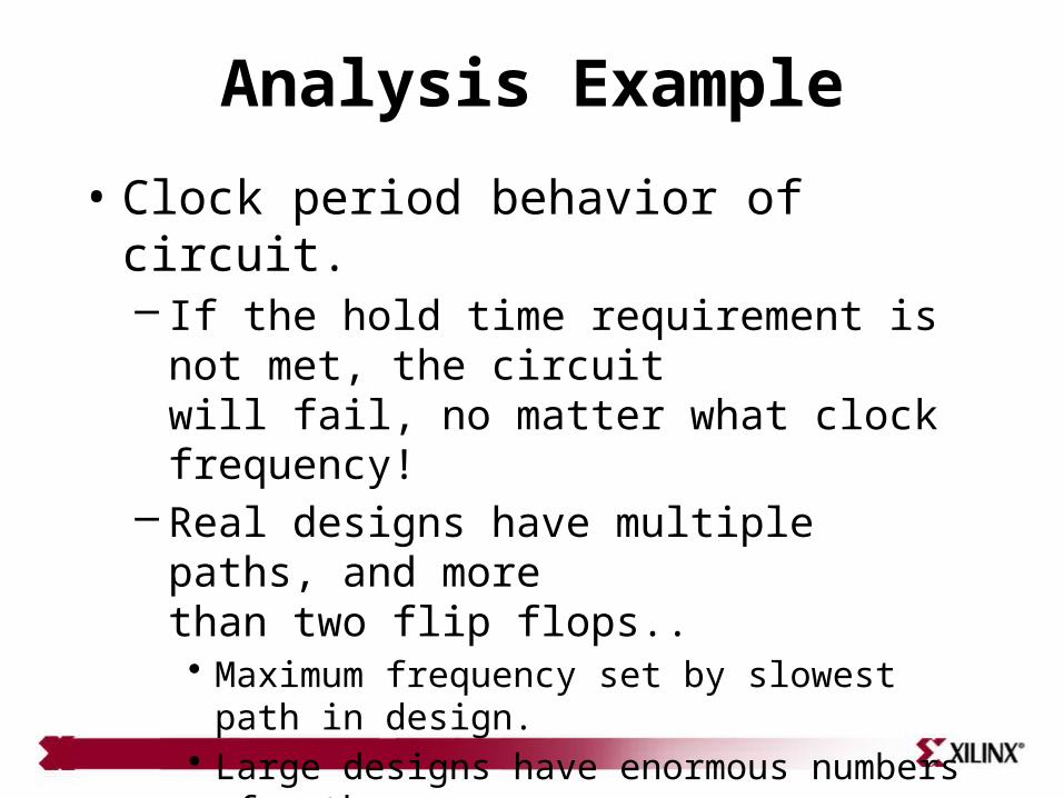
• Clock period behavior of circuit.– If the hold time requirement is not met, the circuit
will fail, no matter what clock frequency!– Real designs have multiple paths, and more
than two flip flops..• Maximum frequency set by slowest path in design.• Large designs have enormous numbers of paths.• Most static timing analysis done by software.

Analysis Example
• Input and output behavior tells us how the circuitinteracts with other circuits and the outside world.
• If device A and device B are synchronous, anyplace an output drives an input, a new path mustbe considered in the period analysis.
D Q
FF#2A
D Q
FF#1A
LOGIC D Q
FF#2B
D Q
FF#1B
LOGICCONNECTION
WIRE

Analysis Example
• The manufacturer of device A does notknow anything about your specific design:– What is device B delay behavior?– What is the delay behavior of wiring?
• Given data on the input and output behaviors...– Minimum and maximum clock to output.– Input setup and hold requirements.
…you can complete the analysis of the paths.
Analysis Example
CLK
OUTPUTD Q
FF#2
D Q
FF#1INPUT
LOGIC
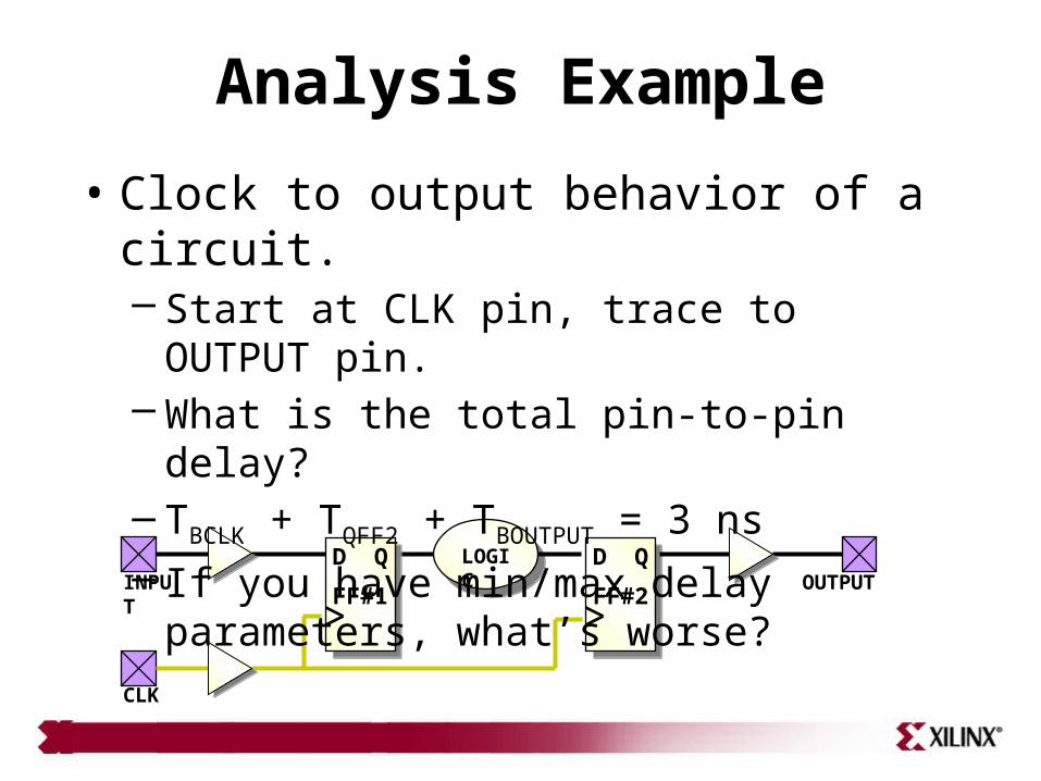
• Clock to output behavior of a circuit.– Start at CLK pin, trace to OUTPUT pin.– What is the total pin-to-pin delay?– TBCLK + TQFF2 + TBOUTPUT = 3 ns– If you have min/max delay parameters, what’s worse?

Analysis Example
CLK
OUTPUTD Q
FF#2
D Q
FF#1INPUT
LOGIC
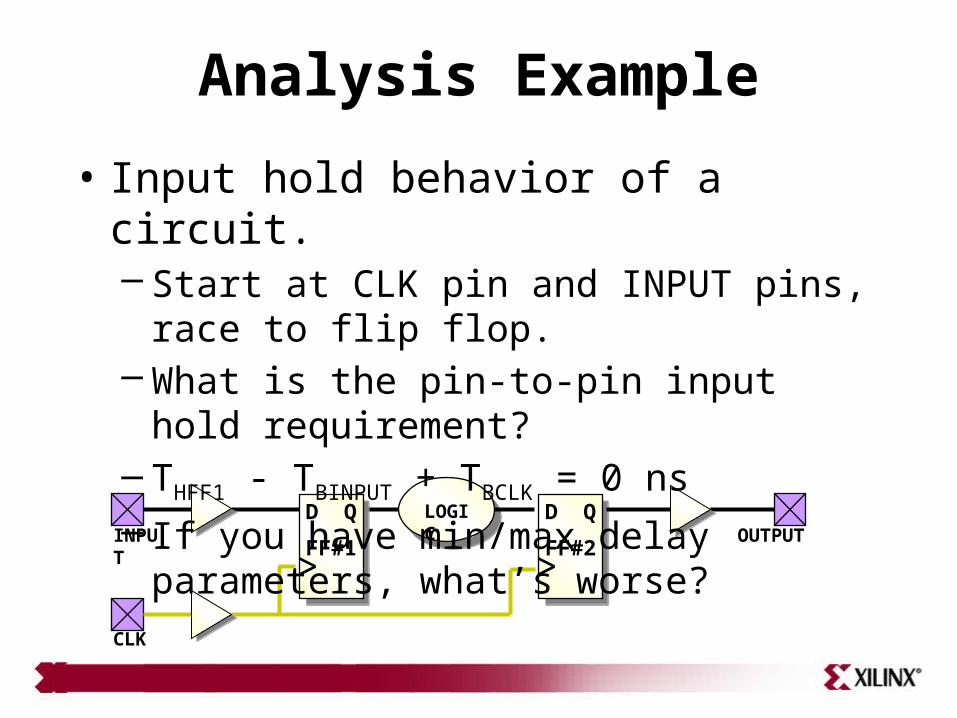
• Input setup behavior of a circuit.– Start at CLK pin and INPUT pins, race to flip flop.– What is the pin-to-pin input setup requirement?– TSUFF1 + TBINPUT - TBCLK = 2 ns– If you have min/max delay parameters, what’s worse?
Analysis Example
CLK
OUTPUTD Q
FF#2
D Q
FF#1INPUT
LOGIC
• Input hold behavior of a circuit.– Start at CLK pin and INPUT pins, race to flip flop.– What is the pin-to-pin input hold requirement?– THFF1 - TBINPUT + TBCLK = 0 ns– If you have min/max delay parameters, what’s worse?
Analysis Example
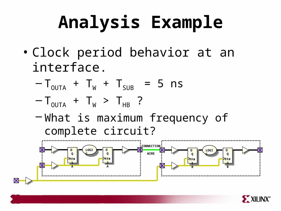
• Clock period behavior at an interface.– TOUTA + TW + TSUB = 5 ns– TOUTA + TW > THB ?– What is maximum frequency of complete circuit?
D Q
FF#2A
D Q
FF#1A
LOGIC D Q
FF#2B
D Q
FF#1B
LOGICCONNECTION
WIRE
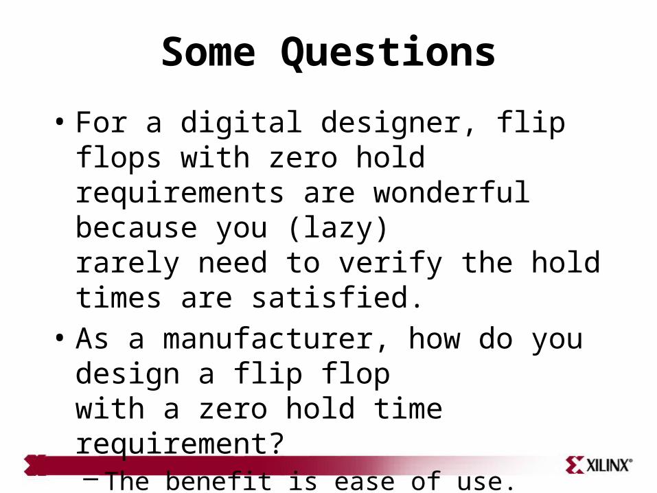
Some Questions
• For a digital designer, flip flops with zero holdrequirements are wonderful because you (lazy)rarely need to verify the hold times are satisfied.
• As a manufacturer, how do you design a flip flopwith a zero hold time requirement?– The benefit is ease of use.– What is the hidden cost?
• As combinational logic and wire delays approachzero, what sets the maximum frequency?
Timing Constraints
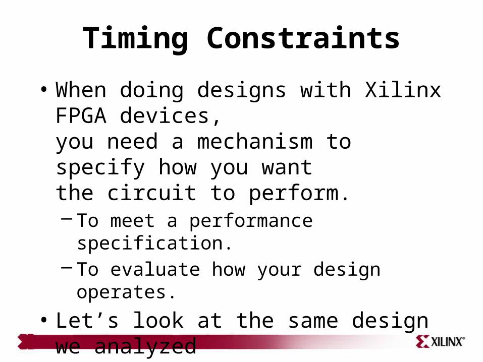
• When doing designs with Xilinx FPGA devices,you need a mechanism to specify how you wantthe circuit to perform.– To meet a performance specification.– To evaluate how your design operates.
• Let’s look at the same design we analyzedmanually and see how to use the static timinganalyzer provided by Xilinx.
Timing Constraints
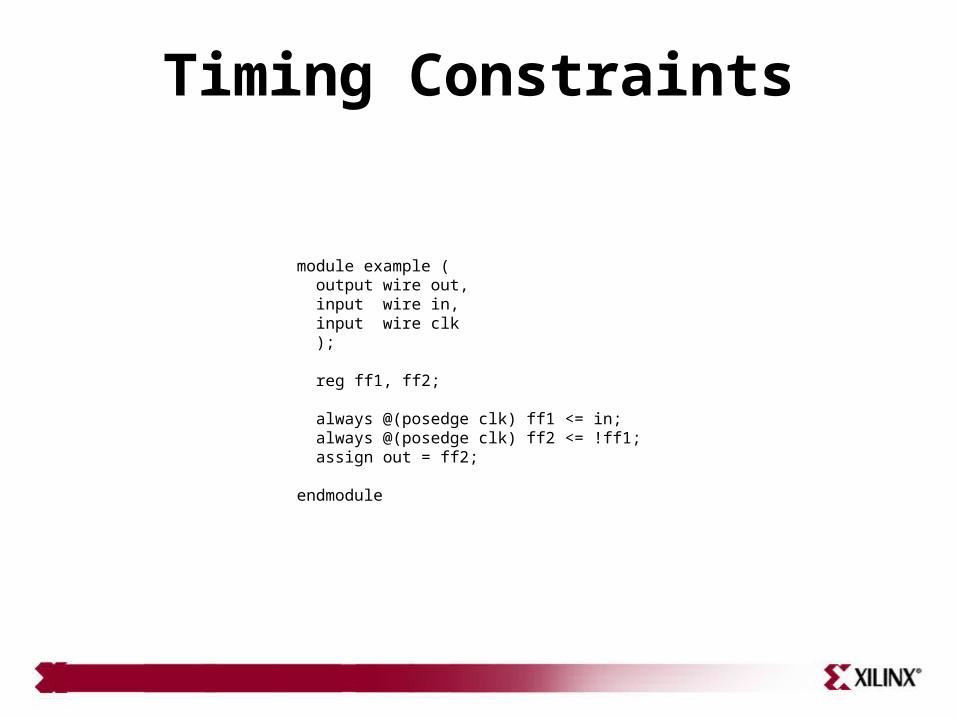
module example ( output wire out, input wire in, input wire clk );
reg ff1, ff2;
always @(posedge clk) ff1 <= in; always @(posedge clk) ff2 <= !ff1; assign out = ff2;
endmodule
Timing Constraints
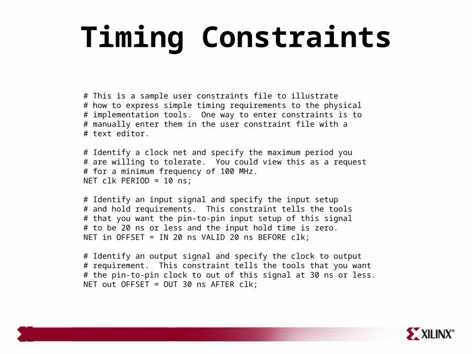
# This is a sample user constraints file to illustrate# how to express simple timing requirements to the physical# implementation tools. One way to enter constraints is to# manually enter them in the user constraint file with a# text editor.
# Identify a clock net and specify the maximum period you# are willing to tolerate. You could view this as a request# for a minimum frequency of 100 MHz.NET clk PERIOD = 10 ns;
# Identify an input signal and specify the input setup# and hold requirements. This constraint tells the tools# that you want the pin-to-pin input setup of this signal# to be 20 ns or less and the input hold time is zero.NET in OFFSET = IN 20 ns VALID 20 ns BEFORE clk;
# Identify an output signal and specify the clock to output# requirement. This constraint tells the tools that you want# the pin-to-pin clock to out of this signal at 30 ns or less.NET out OFFSET = OUT 30 ns AFTER clk;

Timing Constraints
• When the place and route program finishes,it will provide you with a summary of yourtiming requirements (pass/fail indicator).
• You can then run the static timing analyzer,which can give you a verbose analysis ofyour design.
• Let’s take a look...
Timing Constraints
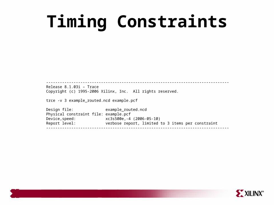
--------------------------------------------------------------------------------Release 8.1.03i – TraceCopyright (c) 1995-2006 Xilinx, Inc. All rights reserved.
trce -v 3 example_routed.ncd example.pcf
Design file: example_routed.ncdPhysical constraint file: example.pcfDevice,speed: xc3s500e,-4 (2006-05-10)Report level: verbose report, limited to 3 items per constraint--------------------------------------------------------------------------------

Timing Constraints================================================================================Timing constraint: NET "clk_BUFGP/IBUFG" PERIOD = 10 nS HIGH 50.000000 % ;
1 item analyzed, 0 timing errors detected. Minimum period is 3.410ns.--------------------------------------------------------------------------------Slack: 6.590ns (requirement - (data path - negative clock skew)) Source: ff1 Destination: ff2 Requirement: 10.000ns Data Path Delay: 3.410ns (Levels of Logic = 3) Negative Clock Skew: 0.000ns Source Clock: clk_BUFGP rising at 0.000ns Destination Clock: clk_BUFGP rising at 10.000ns
Data Path: ff1 to ff2 Location Delay type Delay(ns) Physical Resource Logical Resource(s) ------------------------------------------------- ------------------- SLICE_X18Y30.YQ Tcko 0.992 ff2 ff1 SLICE_X18Y30.G3 net (fanout=1) 0.421 ff1 SLICE_X18Y30.Y Tilo 0.468 N8 I_INV_ff1/LUT1_L_BUF SLICE_X18Y30.BX net (fanout=1) 0.805 N8 SLICE_X18Y30.CLK Tdick 0.724 ff2 ff2 ------------------------------------------------- --------------------------- Total 3.410ns (2.184ns logic, 1.226ns route) (64.0% logic, 36.0% route)
--------------------------------------------------------------------------------
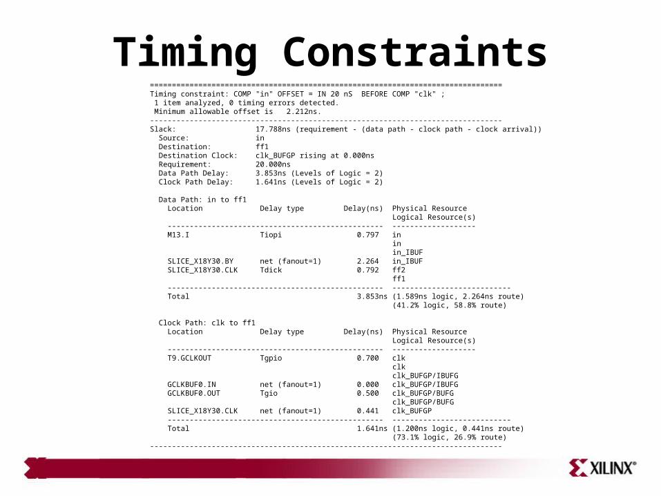
Timing Constraints================================================================================Timing constraint: COMP "in" OFFSET = IN 20 nS BEFORE COMP "clk" ; 1 item analyzed, 0 timing errors detected. Minimum allowable offset is 2.212ns.--------------------------------------------------------------------------------Slack: 17.788ns (requirement - (data path - clock path - clock arrival)) Source: in Destination: ff1 Destination Clock: clk_BUFGP rising at 0.000ns Requirement: 20.000ns Data Path Delay: 3.853ns (Levels of Logic = 2) Clock Path Delay: 1.641ns (Levels of Logic = 2)
Data Path: in to ff1 Location Delay type Delay(ns) Physical Resource Logical Resource(s) ------------------------------------------------- ------------------- M13.I Tiopi 0.797 in in in_IBUF SLICE_X18Y30.BY net (fanout=1) 2.264 in_IBUF SLICE_X18Y30.CLK Tdick 0.792 ff2 ff1 ------------------------------------------------- --------------------------- Total 3.853ns (1.589ns logic, 2.264ns route) (41.2% logic, 58.8% route)
Clock Path: clk to ff1 Location Delay type Delay(ns) Physical Resource Logical Resource(s) ------------------------------------------------- ------------------- T9.GCLKOUT Tgpio 0.700 clk clk clk_BUFGP/IBUFG GCLKBUF0.IN net (fanout=1) 0.000 clk_BUFGP/IBUFG GCLKBUF0.OUT Tgio 0.500 clk_BUFGP/BUFG clk_BUFGP/BUFG SLICE_X18Y30.CLK net (fanout=1) 0.441 clk_BUFGP ------------------------------------------------- --------------------------- Total 1.641ns (1.200ns logic, 0.441ns route) (73.1% logic, 26.9% route)--------------------------------------------------------------------------------

Timing Constraints================================================================================Timing constraint: COMP "out" OFFSET = OUT 30 nS AFTER COMP "clk" ; 1 item analyzed, 0 timing errors detected. Minimum allowable offset is 8.740ns.--------------------------------------------------------------------------------Slack: 21.260ns (requirement - (clock arrival + clock path + data path)) Source: clk Destination: out Source Clock: clk_BUFGP rising at 0.000ns Requirement: 30.000ns Data Path Delay: 7.099ns (Levels of Logic = 2) Clock Path Delay: 1.641ns (Levels of Logic = 2)
Clock Path: clk to ff2 Location Delay type Delay(ns) Physical Resource Logical Resource(s) ------------------------------------------------- ------------------- T9.GCLKOUT Tgpio 0.700 clk clk clk_BUFGP/IBUFG GCLKBUF0.IN net (fanout=1) 0.000 clk_BUFGP/IBUFG GCLKBUF0.OUT Tgio 0.500 clk_BUFGP/BUFG clk_BUFGP/BUFG SLICE_X18Y30.CLK net (fanout=1) 0.441 clk_BUFGP ------------------------------------------------- --------------------------- Total 1.641ns (1.200ns logic, 0.441ns route) (73.1% logic, 26.9% route)
Data Path: ff2 to out Location Delay type Delay(ns) Physical Resource Logical Resource(s) ------------------------------------------------- ------------------- SLICE_X18Y30.XQ Tcko 0.992 ff2 ff2 K12.O net (fanout=1) 1.506 ff2 K12.PAD Tioop 4.601 out out_OBUF out ------------------------------------------------- --------------------------- Total 7.099ns (5.593ns logic, 1.506ns route) (78.8% logic, 21.2% route)--------------------------------------------------------------------------------
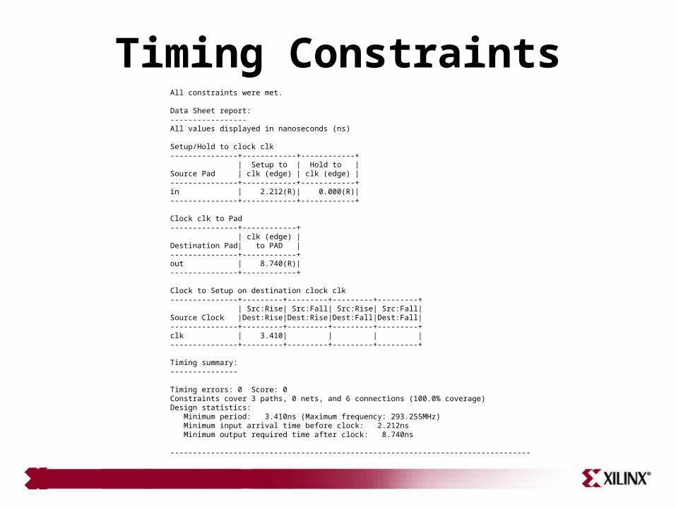
Timing ConstraintsAll constraints were met.
Data Sheet report:-----------------All values displayed in nanoseconds (ns)
Setup/Hold to clock clk---------------+------------+------------+ | Setup to | Hold to |Source Pad | clk (edge) | clk (edge) |---------------+------------+------------+in | 2.212(R)| 0.000(R)|---------------+------------+------------+
Clock clk to Pad---------------+------------+ | clk (edge) |Destination Pad| to PAD |---------------+------------+out | 8.740(R)|---------------+------------+
Clock to Setup on destination clock clk---------------+---------+---------+---------+---------+ | Src:Rise| Src:Fall| Src:Rise| Src:Fall|Source Clock |Dest:Rise|Dest:Rise|Dest:Fall|Dest:Fall|---------------+---------+---------+---------+---------+clk | 3.410| | | |---------------+---------+---------+---------+---------+
Timing summary:---------------
Timing errors: 0 Score: 0Constraints cover 3 paths, 0 nets, and 6 connections (100.0% coverage)Design statistics: Minimum period: 3.410ns (Maximum frequency: 293.255MHz) Minimum input arrival time before clock: 2.212ns Minimum output required time after clock: 8.740ns
--------------------------------------------------------------------------------
Timing Constraints
• How about input hold requirements?– These paths are reported if failures occur.
• How about minimum clock to out requirements?– Typically, if you care about minimum clock to out,
you can use the dedicated IOB output flip flops,which have their output behavior tabulated in theFPGA device datasheet.
– Another way is to analyze the circuit again, usingthe “min” speed grade.