ee109 digital circuitsbytes.usc.edu/files/ee109/slides/ee109unit2_digitalcircuits.pdf · nd. gen....
TRANSCRIPT

2.1
Unit 2
Digital Circuits (Logic)

2.2
ANALOG VS. DIGITALMoving from voltages to 1's and 0's…
2.3
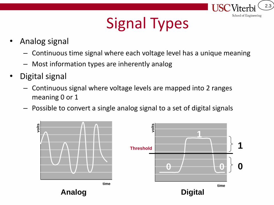
Signal Types• Analog signal
– Continuous time signal where each voltage level has a unique meaning
– Most information types are inherently analog
• Digital signal– Continuous signal where voltage levels are mapped into 2 ranges
meaning 0 or 1
– Possible to convert a single analog signal to a set of digital signals
0
1
0
1
0
vo
lts
vo
lts
timetime
Analog Digital
Threshold

2.4
Signals and Meaning
0.0 V
0.8 V
2.0 V
5.0 V
Each voltage value
has unique meaning
0.0 V
5.0 V
Lo
gic
1L
og
ic 0
Ille
gal
Analog Digital
Threshold Range
Each voltage maps to '0' or '1'
(There is a small illegal range where meaning is
undefined since threshold can vary based on
temperature, small variations in manufacturing, etc.)

2.5
Analog vs. DigitalUSC students used to program analog computers!

2.6
COMPUTERS AND SWITCHING TECHNOLOGY
A Brief History
2.7
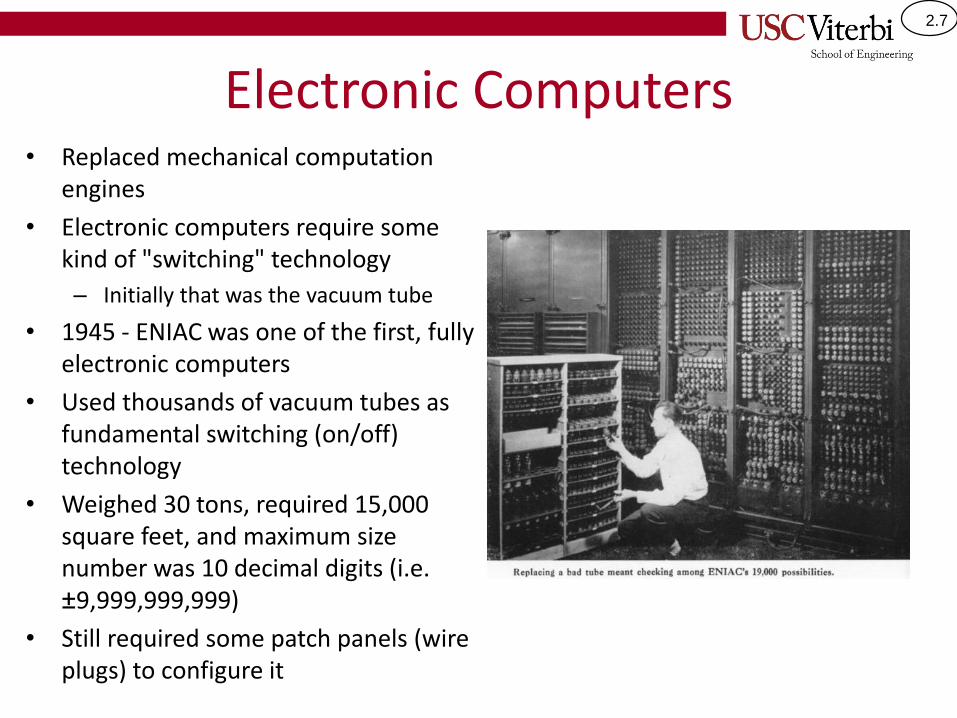
Electronic Computers• Replaced mechanical computation
engines
• Electronic computers require some kind of "switching" technology
– Initially that was the vacuum tube
• 1945 - ENIAC was one of the first, fully electronic computers
• Used thousands of vacuum tubes as fundamental switching (on/off) technology
• Weighed 30 tons, required 15,000 square feet, and maximum size number was 10 decimal digits (i.e. ±9,999,999,999)
• Still required some patch panels (wire plugs) to configure it

2.8
Vacuum Tube Technology• Digital, electronic computers use some sort of
voltage controlled switch (on/off)
• Looks like a light bulb
• Usually 3 nodes– 1 node serves as the switch value allowing current to flow
between the other 2 nodes (on) or preventing current flow between the other 2 nodes (off)
– Example: if the switch input voltage is 5V, then current is allowed to flow between the other nodes
Vacuum Tube
Switch
Input
(Hi or Lo
Voltage)
A
B
Current can flow
based on voltage
of input switch

2.9
Vacuum Tube Disadvantages
• Relatively large
– Especially when you need 19,000 to make 1 computer
• Unreliable
– Can burn out just like a light bulb
• Dissipate a lot of heat (power)

2.10
Transistor• Another switching device
• Invented by Bell Labs in 1948
• Uses semiconductor materials (silicon)
• Much smaller, faster, more reliable (doesn't burn out), and dissipated less power
Individual Transistors
(About the size of your fingertip)
Transistor
is 'on'
Transistor
is 'off'
Gate
+5V
Source Drain
- - - -
--
High voltage at gate allows
current to flow from source to
drain
Gate
0V
Drain
-
Low voltage at gate prevents
current from flowing from
source to drain
-
Silicon
Silicon
Source
Vo
ltag
e a
t th
e g
ate
co
ntr
ols
th
e o
pera
tio
n
of
the
tra
ns
isto
r

2.11
Moore's Law & Transistors
• Moore's Law = Number of transistors able to be fabricated on a chip will double every 1.5 – 2 years (i.e. exponential growth)
– Achieved by shrinking the transistor structure
– However, we are approaching the physical limitations of this shrinking
– 53% compound annual growth rate over 50 years• No other technology has grown so fast so long
• Transistors are the fundamental building block of computer HW
– Switching devices: Can conduct [on = 1] or not-conduct [off = 0] based on an input voltage
2.12
How Does a Transistor Work
• Transistor inner workings
– http://www.youtube.com/watch?v=IcrBqCFLHIY

2.13
NMOS Transistor Physics
• Let's review what we saw in the video…
• Transistor is started by implanting two n-type silicon areas, separated by p-type
n-type silicon (extra
negative charges)
p-type silicon
("extra" positive charges)
-
+
+
+
-
-
-Source
InputDrain
Input

2.14
NMOS Transistor Physics
• A thin, insulator layer (silicon dioxide or just "oxide") is placed over the silicon between source and drain
n-type silicon (extra
negative charges)
Insulator Layer
(oxide)
p-type silicon
("extra" positive charges)
-
+
+
+
-
-
-
Source Input Drain Output

2.15
NMOS Transistor Physics
• A thin, insulator layer (silicon dioxide or just "oxide") is placed over the silicon between source and drain
• Conductive polysilicon material is layered over the oxide to form the gate input
n-type silicon (extra
negative charges)
Insulator Layer
(oxide)
p-type silicon
("extra" positive charges)
conductive
polysilicon
-
+
+
+
-
-
-
Gate InputSource Input Drain Output

2.16
NMOS Transistor Physics
• Positive voltage (charge) at the gate input repels the extra positive charges in the p-type silicon
• Result is a negative-charge channel between the source input and drain
p-type
Gate Input
Source Input Drain Output
n-type
+
+
+
+
+
+ + + +
+ + + +
- - -
negatively-charge
channel
--
positive charge
"repelled"

2.17
NMOS Transistor Physics
• Electrons can flow through the negative channel from the source input to the drain output
• The transistor is "on" p-type
Gate Input
Source Input Drain Output
n-type
+
+
+
+
+
+ + + +
+ + +
-
-
-
- - - --
-
-
+
- -
Negative channel between
source and drain =
Current flow
- -

2.18
NMOS Transistor Physics
• If a low voltage (negative charge) is placed on the gate, no channel will develop and no current will flow
• The transistor is "off" p-type
Gate Input
Source Input Drain Output
n-type
-
-
-
-
-
- - - -
+
+
+
No negative channel
between source and drain
= No current flow
-
-
- --
-
-
+ + +

2.19
View of a Transistor
• Cross-section of transistors on an IC
• Moore's Law is founded on our ability to keep shrinking transistor sizes
– Gate/channel width shrinks
– Gate oxide shrinks
• Transistor feature size is referred to as the implementation "technology node"
Electron Microscope View of Transistor Cross-Section

2.20
Minimum Feature Size

2.21
Intel Processor Trends
1971 – Intel 4004
1000 transistors
Max 4K-bits addressable memory
1 MHz operation
• 2nd Gen. Intel Core i7 Extreme
Processor for desktops launched
in Q4 of 2012
• #cores/#threads: 6/12
• Technology node: 32nm
• Clock speed: 3.5 GHz
• Transistor count: Over one billion
• Cache: 15MB
• Addressable memory: 64GB
• Size: 52.5mm by 45.0mm mm2

2.22
ARM Cortex A15
ARM Cortex A15 in 2011 to 2013
• 4 cores per cluster, two clusters per chip
• Technology node: 22nm
• Clock speed: 2.5 GHz
• Transistor count: Over one billion
• Cache: Up to 4MB per cluster
• Addressable memory: up to 1TB
• Size: 52.5mm by 45.0mm
22

2.23
DIGITAL LOGIC GATES

2.24
Transistors and Logic
• Transistors act as switches (on or off)
• Logic operations (AND / OR) formed by connecting them in specific patterns
– Series Connection
– Parallel Connection
Series Connection
S1 AND S2 must be
on for A to be
connected to B
Parallel Connection
S1 OR S2 must be
on for A to be
connected to B
A BS2S1
A BS1
S2

2.25
Gates
• Each logical operation (AND, OR, NOT) can be implemented as an digital device called a "gate"
– The schematic symbols below are used to represent each logic gate
• Each logic gate can be built by connecting transistors in various configurations
AND Gate OR Gate NOT Gate

2.26
AND Gates• An AND gate outputs a '1' (true) if ALL inputs are '1' (true)
• Gates can have several inputs
• Behavior can be shown in a truth table (listing all possible input combinations and the corresponding output)
Y
XF
X Y F
0 0 0
0 1 0
1 0 0
1 1 1
2-input AND
X Y Z F
0 0 0 0
0 0 1 0
0 1 0 0
0 1 1 0
1 0 0 0
1 0 1 0
1 1 0 0
1 1 1 1
3-input AND
F
X
Y
Z
F=X•Y F=X•Y•Z

2.27
OR Gates
• An OR gate outputs a '1' (true) if ANY input is '1' (true)
• Gates can also have several inputs
Y
XF
X Y F
0 0 0
0 1 1
1 0 1
1 1 1
2-input OR
X Y Z F
0 0 0 0
0 0 1 1
0 1 0 1
0 1 1 1
1 0 0 1
1 0 1 1
1 1 0 1
1 1 1 1
3-input OR
F
X
Y
Z
F=X+Y F=X+Y+Z

2.28
Buffer & NOT (Inverter) Gate
• A Buffer simply passes a digital value
– But strengthens it electrically (e.g. boosts 3.7V closer to 5V)
• A NOT (aka "inverter") gate inverts a digital signal to its opposite value (i.e. flips a bit)
X F
X F
1 0
0 1
F = X
the "bubble" (logically
performs the inversion)
X F
0 0
1 1
F = X
X F

2.29
Aside: How Do You Build an Inverter (1)?
• A simple (though maybe not ideal) method to build an inverter is to place a transistor in series with a resistor– Input to inverter is input to transistor
– Output of inverter is node between resistor and transistor
• We can model the transistor as a resistor
• Develop an equation for Vout
Vdd
GND
Vin
Vout
Rpullup
Vdd
GND
Vin
Vout
Rpullup
RTrans
VoutVin
𝑉𝑜𝑢𝑡 = 𝑉𝑑𝑑 ∗𝑅𝑡𝑟𝑎𝑛𝑠
𝑅𝑡𝑟𝑎𝑛𝑠 + 𝑅𝑝𝑢𝑙𝑙𝑢𝑝

2.30
Aside: How Do You Build an Inverter (2)?
• First, estimate the resistance of Rtrans if Vin is 0 (low) then again if Vin is 1 (high-voltage)
• Use that estimate in your equation for Vout to determine the output voltage
Vdd
GND
0
Vout = ____
Rpullup
Rtrans = ____
Vdd
GND
1
(Vdd)
Rpullup
Rtrans = ____
Vout = ____
2.31
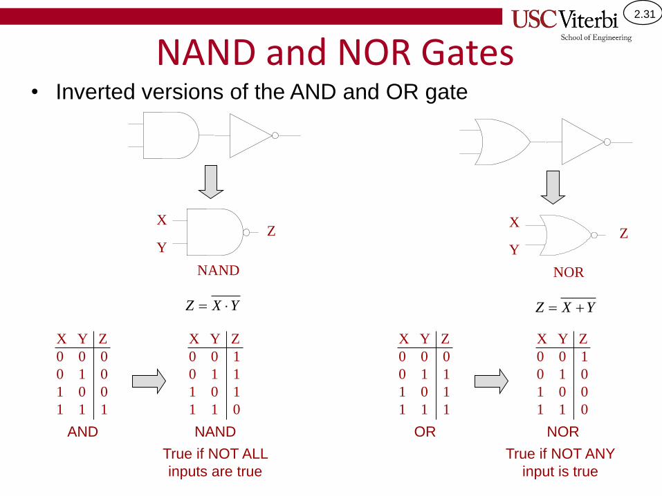
NAND and NOR Gates
NAND NOR
ZX
YZ
X Y Z
0 0 1
0 1 0
1 0 0
1 1 0
X
Y
X Y Z
0 0 1
0 1 1
1 0 1
1 1 0
YXZ YXZ
X Y Z
0 0 0
0 1 0
1 0 0
1 1 1
X Y Z
0 0 0
0 1 1
1 0 1
1 1 1
AND NAND OR NOR
True if NOT ANY
input is true
True if NOT ALL
inputs are true
• Inverted versions of the AND and OR gate

2.32
XOR and XNOR Gates
XOR
FX
Y
X Y F
0 0 0
0 1 1
1 0 1
1 1 0
XNOR
FX
Y
X Y F
0 0 1
0 1 0
1 0 0
1 1 1
YXF YXF
True if an odd # of inputs are true
= True if inputs are different
True if an even # of inputs are true
= True if inputs are same
➢ Exclusive OR gate. Outputs a '1' if either input is a
'1', but not both.
X Y Z F
0 0 0 0
0 0 1 1
0 1 0 1
0 1 1 0
1 0 0 1
1 0 1 0
1 1 0 0
1 1 1 1
X
Y
Z
F
X Y Z F
0 0 0 1
0 0 1 0
0 1 0 0
0 1 1 1
1 0 0 0
1 0 1 1
1 1 0 1
1 1 1 0
X
Y
Z
F

2.33
A
B
C
D
F
Logic Example
10
0
1
0 01
0
1

2.34
Logic Example
00
1
0
0 11
1
1A
B
C
D
F

2.35
Practice: Waveform Diagrams
• Waveform diagrams show digital circuit operation over time
– Vertical axis: Each signal can be HIGH (1) or LOW (0)
– Horizontal axis: time
• Complete the waveform for the given circuit
F
A
B
C
x
y
w
A
B
C
x
F
y
wNOT of B
A and w
B or C
x xor y

2.36
BOOLEAN ALGEBRA INTRO
2.37
Boolean Algebra Intro
• Larger logic circuits are too complex to analyze with truth tables or schematics
• Instead, use mathematical notation (equations) and develop axioms and theorems to help us manipulate logical expressions/equations
– Axioms = Basis / assumptions used
– Theorems = manipulations that we can use

2.38
Axioms
• Axioms are the basis for Boolean Algebra
• Notice that these axioms are simply restating our definition of digital/binary logic– A1/A1’ = Binary variables (only 2 values possible)
– A2/A2’ = NOT operation
– A3,A4,A5 = AND operation
– A3’,A4’,A5’ = OR operation
(A1) X = 0 if X ≠ 1 (A1’) X = 1 if X ≠ 0
(A2) If X = 0, then X’ = 1 (A2’) If X = 1, then X’ = 0
(A3) 0 • 0 = 0 (A3’) 1 + 1 = 1
(A4) 1 • 1 = 1 (A4’) 0 + 0 = 0
(A5) 1 • 0 = 0 • 1 = 0 (A5’) 0 + 1 = 1 + 0 = 1

2.39
Duality
• Every truth statement can yields another truth statement– I exercise if I have time and energy (original statement)
– I don’t exercise if I don’t have time or don’t have energy (dual
statement)
• To express the dual, swap…
1’s
•
0’s
+

2.40
Duality
• The “dual” of an expression is not equal to the original
• Taking the “dual” of both sides of an equation yields a new equation
1 + 0 0 • 1Original
expression
Dual≠
X + 1 = 1
Original equation Dual
X • 0 = 0

2.41
Single Variable Theorems
• Provide some simplifications for expressions containing:– a single variable
– a single variable and a constant bit
• Each theorem has a dual (another true statement)
• Each theorem can be proved by writing a truth table for both sides (i.e. proving the theorem holds for all possible values of X)
T1 X + 0 = X T1' X • 1 = X
T2 X + 1 = 1 T2' X • 0 = 0
T3 X + X = X T3' X • X = X
T4 (X')' = X
T5 X + X' = 1 T5' X • X' = 0

2.42
Single Variable Theorem (T1)
X+0 = X (T1) X•1 = X (T1’)
X Y Z
0 0 0
0 1 1
1 0 1
1 1 1
X Y Z
0 0 0
0 1 0
1 0 0
1 1 1
OR AND
Whenever a variable is OR’ed with 0,
the output will be the same as the
variable…
“0 OR Anything equals that
anything”
Whenever a variable is AND’ed with
1, the output will be the same as the
variable…
“1 AND Anything equals that
anything”
Hold Y
constant

2.43
Single Variable Theorem (T2)
X+1 = 1 (T2) X•0 = 0 (T2’)
X Y Z
0 0 0
0 1 1
1 0 1
1 1 1
X Y Z
0 0 0
0 1 0
1 0 0
1 1 1
OR AND
Whenever a variable is OR’ed with 1,
the output will be 1…
“1 OR anything equals 1”
Whenever a variable is AND’ed with
0, the output will be 0…
“0 AND anything equals 0”
Hold Y
constant

2.44
Single Variable Theorem (T3)
X+X = X (T3) X•X = X (T3’)
X Y Z
0 0 0
0 1 1
1 0 1
1 1 1
X Y Z
0 0 0
0 1 0
1 0 0
1 1 1
OR AND
Whenever a variable is OR’ed with
itself, the result is just the value of the
variable
Whenever a variable is AND’ed with
itself, the result is just the value of the
variable
This theorem can be used to reduce two identical terms into one
OR to replicate one term into two.

2.45
Single Variable Theorem (T4)
(X’)’ = X (T4)
Anything inverted twice yields its original value
(X) = X (T4)
0 1 0

2.46
Single Variable Theorem (T5)
X+X = 1 (T5) X•X = 0 (T5’)
X Y Z
0 0 0
0 1 1
1 0 1
1 1 1
X Y Z
0 0 0
0 1 0
1 0 0
1 1 1
OR AND
Whenever a variable is OR’ed with its
complement, one value has to be 1
and thus the result is 1
This theorem can be used to simplify variables into a constant or to
expand a constant into a variable.
Whenever a variable is AND’ed with
its complement, one value has to be
0 and thus the result is 0

2.47
Practice
• Exercise 1: Given the circuit below, write the corresponding logic equation for Y
• Exercise 2: Suppose we learn S=0, simply the equation for Y using T1-T5
• Exercise 3: Suppose we learn S=1, simply the equation for Y using T1-T5
IN0
S
IN1
Y

2.48
Application: Channel Selector
• Given 4 input, digital music/sound channels and 4 output channels
• Given individual “select” inputs that select 1 input channel to be routed to 1 output channel
Channel
Selector
ICH0
ICH1
ICH2
ICH3
OCH0
OCH1
OCH2
OCH3
ISE
L0
ISE
L1
ISE
L2
ISE
L3
OS
EL
0
OS
EL
1
OS
EL
2
OS
EL
3
4 Input channels
4 Output
channels
Input
Channel
Select
Output
Channel
Select
011010101001101
101010110101010
101001010101111
001010101001011

2.49
Application: Steering Logic
• 4-input music channels (ICHx)
– Select one input channel (use ISELx inputs)
– Route to one output channel (use OSELx inputs)
011010101001101
101010110101010
101001010101111
001010101001011
ICH 0
ICH 1
ICH 2
ICH 3
ISE
L0
ISE
L1
ISE
L2
ISE
L3
OS
EL0
OS
EL
1
OS
EL
2
OS
EL
3
OCH 0
OCH 1
OCH 2
OCH 3
2.50
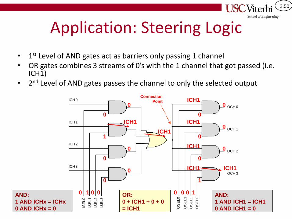
Application: Steering Logic
• 1st Level of AND gates act as barriers only passing 1 channel• OR gates combines 3 streams of 0’s with the 1 channel that got passed (i.e.
ICH1)• 2nd Level of AND gates passes the channel to only the selected output
ICH 0
ICH 1
ICH 2
ICH 3
ISE
L0
I SE
L1
I SE
L2
I SE
L3
OS
EL0
OS
EL
1
OS
EL
2
OS
EL
3
OCH 0
OCH 1
OCH 2
OCH 3
0 0 0 1
0
0
0
1
0
0
0
ICH1
ICH1
1
0
0
0
ICH1
ICH1
ICH1
ICH1 ICH1
0
0
0
0 1 0 0 OR:
0 + ICH1 + 0 + 0
= ICH1
AND:
1 AND ICH1 = ICH1
0 AND ICH1 = 0
AND:
1 AND ICHx = ICHx
0 AND ICHx = 0
Connection
Point

2.51
DIGITAL DESIGN GOALSSpeed, area, and power

2.52
Digital Design Goals
• When designing a circuit, we want to optimize for the following three things:– Area or Circuit Size (minimize)
– Speed (maximize) or Delay (minimize)
– Power (minimize)
• Can usually only optimize one or two of the 3– There is a huge trade space! This is what engineering is all about!

2.53
Minimizing Circuit Area
• Approaches:
– Reduce the number of gates used to implement a circuit
– Reduce the number of inputs to each gate
• In general a gate with n inputs requires 2*n transistors to implement
• Simplify logic expressions (usually by factoring and then canceling terms) to reduce the number of gates
– We'll learn more about this soon

2.54
Maximizing Speed
• Speed is affected by:
– Levels of logic (path length)
– Gate type
– Number of inputs (fan-in) to the gate
– Number of outputs a gate connects to (fan-out)
– Feature size and implementation technology

2.55
Delay Example• Levels of Logic = Max. # of gates on any path
from input to output
00
1
0
0 11
1
1A
B
C
D
F
1 00
0
1
4 Levels of Logic
Change in D, C, or A must propagate
through 4 levels of gates

2.56
Gate Delays
• Order the gate types in terms of fastest to slowest?
• Typical gate delay for a 2-input NAND or NOR is under a 100 ps.
ZX
YZ
X
Y
ZX
YZ
X
Y
X Z
X
YZ Z
X
Y
1
2
3
4

2.57
Logical Operations Summary• All digital circuits can be described using AND, OR,
and NOT– Note: You'll learn in future courses that digital circuits
can be described with any of the following sets: • {AND, NOT}, {OR, NOT}, {NAND only}, or {NOR only}
• Normal convention: 1 = true / 0 = false
• A logic circuit takes some digital inputs and transforms each possible input combination to a desired output values
Logic
CircuitI0
I1
I2
O0
O1
Inputs Outputs
Trivia-of-the-day: The Apollo
Guidance Computer that
controlled the lunar spacecraft in
1969 was built out of 8,400
3-input NOR gates.

2.58
SEQUENTIAL LOGICStoring bits

2.59
Combinational vs. Sequential Logic
• All logic is categorized into 2 groups
– Combinational logic:
• Outputs = f(current inputs)
– Sequential Logic
• Outputs = f(current + past inputs)
• Sequential logic has the notion of “memory” (remembering inputs or events that happened in the past)

2.60
Combinational vs. Sequential
Outputs depend only on current
outputs
Outputs depend on current inputs
and previous inputs (previous
inputs summarized via state)
Current inputs Outputs
Currentinputs
Outputs
1 0 1
Sequential Outputs (State)
feedback as inputs
Sequential Inputs
(Next State)
Combinational
Logic
Combinational
Logic
Sequential Logic

2.61
Combinational Example: Staircase Light Switch
Whether or not the light is
on is only dependent on
the current position of the
switches
S1
S2
Light
Logic
CircuitLight
S1
S2
S1 S2 Light
0 0
0 1
1 0
1 1

2.62
Water Tank Problem
• Build a control system for a pump to keep the tank from going empty
Sensor
Low
Sensor
Pump Pump
High
Sensor

2.63
Sequential Devices (Registers)
• AND, OR, NOT, NAND, and other gates are known as combinational logic– Outputs only depend on what the inputs are right now, not one second ago
– This implies they have no "memory" (can't remember a value)
• Sequential logic devices provide the ability to retain or "remember" a value by itself (even after the input is changed or removed)– Outputs can depend on the current inputs, and previous states of the
circuit (stored values.)
– Usually have a controlling signal that indicates when the device should update the value it is remembering vs. when it should simply remember that value
– This controlling signal is usually the "clock" signal

2.64
Registers• Registers are the most common sequential
device
• Registers sample the data input (D) on the edge of a clock pulse (CP) and stores that value at the output (Q)
• Analogy: Taking a picture with your phone…when you press a button (clock pulse) the camera samples the scene (input) and remembers/saves it as a snapshot (output). A register can only save 1 value (i.e. the last picture taken)
t = 0 ns t = 1 ns t = 5 ns t = 7 ns t = 10 ns
Clock pulse
q(t) d(1) d(5) d(7) d(10)unk
d(t)
Some input value changing over time
d(1) d(2) d(3) d(4) d(5) d(6) d(7) d(8) d(9) d(10) d(11) d(12)
D
Q
CPClock pulse
Data Input
Data Output
(could be
many bits)
(could be
many bits)
Block Diagram of
a Register
The clock pulse
(positive edge)
here…
…causes q(t) to
sample and hold
the current d(t)
value

2.65
d(t)
q(t)
Clock pulse
Flip-Flops
• Flip-flops are the building blocks of registers– 1 Flip-flop PER bit of input/output
– There are many kinds of flip-flops but the most common is the D- (Data) Flip-flop (a.k.a. D-FF)
• D Flip-flop triggers on the clock edge and captures the D-value at that instant and causes Q to remember it until the next edge– Positive Edge: instant the clock transition from low to high (0 to 1)
Positive-Edge Triggered
D-FF
D Q
CLK
D-FFClock Signal
d(t) q(t)

2.66
Registers and Flip-flops
• A register is simply a group of D flip-flops that all trigger on a single clock pulse
D Q
D Q
D Q
D Q
CP
D3
D2
D1
D0
Q3
Q2
Q1
Q0
D-FF
D-FF
D-FF
D-FF
4-bit Register
CLK Qt+1
0 Qt
1 Qt
↑ Dt
Steady level of 0
or 1
Positive Edge

2.67
Pulses and Clocks
• Registers need an edge to trigger
• We can generate pulses at specific times (creating an irregular pattern) when we know the data we want has arrived
• Other registers in our hardware should trigger at a regular interval
• For that we use a clock signal…
– Alternating high/low voltage pulse train
– Controls the ordering and timing of operations performed in the processor
– 1 cycle is usually measured from rising/positive edge to rising/positive edge
• Clock frequency (F) = # of cycles per second
• Clock Period (T) = 1 / Freq.
Processor
Clock Signal
0 (0V)
1 (5V)
1 cycle
2.8 GHz
= 2.8*109 cycles per second
= 0.357 ns/cycle
Op. 1 Op. 2 Op. 3
Clock Pulses

2.68
Combinational vs. Sequential
• Sequential logic (i.e. registers) is used to store values
– Each register is analogous to a variable in your software program (a variable stores a number until you need it)
• Combinational logic is used to process bits (i.e. perform operations on values
– Analogous to operators (+,-,*) in your software program