ee 6303 linear integrated circuits and · pdf filethe figure shown below is a positive voltage...
TRANSCRIPT

EE 6303 – LINEAR INTEGRATED CIRCUITS AND APPLICATIONS
PART - A
UNIT 5
1. Define Line regulation and Load regulation. [ND – 2015]
Line regulation is a measure of the ability of the power supply to maintain its output voltage given
changes in the input line voltage. Line regulation is expressed as percent of change in the output
voltage relative to the change in the input line voltage.
Load regulation is the capability to maintain a constant voltage (or current) level on the output
channel of a power supply despite changes in the supply's load (such as a change in resistance value
connected across the supply output).
2. What is a switching regulator? (A/M-17)
Switching regulators are those which operate the power transistor as a high frequency on/off switch, so
that the power transistor does not conduct current continuously. This gives improved efficiency over
series regulators.
3. What is the purpose of having input and output capacitors in three terminal IC regulators?
(M/J 16)
A capacitor connected between the input terminal and ground cancels the inductive effects due to long
distribution leads. The output capacitor improves the transient response.
4. What are the advantages of monolithic switching regulators? (M/J 16)
the power transistor is made to operate as low impedance switch.
Power transmitted across the transistor is in discrete pulses rather than as a steady current flow.
increased so as to reduce the size and weight of the inductors and capacitors
5. What is an isolation amplifier? (N/D 16)
An isolation amplifier is an amplifier that offers electrical isolation between its input and output
terminals.
6. What is the advantage of switching regulators? (N/D 16)
Greater efficiency is achieved as the power transistor is made to operate as low impedance switch.
Power transmitted across the transistor is in discrete pulses rather than as a steady current flow. By
using suitable switching loss reduction technique, the switching frequency can be increased so as to
reduce the size and weight of the inductors and capacitors.
7. Where does the thermal noise occur? What is the cause? (N/D 16)
Thermal noise occurs in all passive resistors including the stray series resistances of practical inductors
and capacitors. Thermal noise is due to the random thermal motion of electrons.
8. Define ripple rejection. (N/D 14)
Ripple rejection is a measure of a regulator’s ability to reject ripple voltage. It is expressed in db

9. What is a voltage regulator? (A/M-17)
A voltage regulator is an electronic circuit that provides a stable DC voltage independent of the load
current, independent of the load current, temperature and AC line voltage variations
10. List the main advantages of voltage regulators. (N/D 16)
The main advantages of voltage regulators are:
11. Write the uses of voltage regulators. (A/M-17)
Voltage regulators are commonly used for on-card regulation and laboratory type power switches.
Switch type regulators are used as control circuits in pulse width modulation, Push Pull Bridge and
series type switch mode supplies.
PART – B (80 marks)
11. (a) (i) Draw and explain the functional diagram of 723 IC regulator. (8) [ND – 2015]
The functional diagram of the voltage regulator is shown below. It consists of a
voltage reference source (Pin 6), an error amplifier with its inverting input on pin 4 and non-
inverting input on pin 5, a series pass transistor (pins 10 and 11), and a current limiting
transistor on pins 2 and 3. The device can be set to work as both posistive and negaive voltage
regulators with an output voltage ranging from 2 V to 37 V, and output current levels upto
150 m A. The maximum supply voltage is 40 V, and the line and load regulations are each
specified as 0.01%.

The figure shown below is a positive voltage regulator with an IC 723. The output
voltage can be set to any desired positive voltage between (7-37) volts. 7 volts is the reference
starting voltage. All these variations are brought with the change of values in resistors R1 and
R2 with the help of a potentiometer. A darlington connection is made by the transistor to Q1
to handle large load current. The broken lines in the image indicate the internal connections
for current limiting. Even foldback current limiting is possible in this IC. A regulator output
voltage less than the 7 V reference level can be obtained by using a voltage divider across the
reference source. The potentially divided reference voltage is then connected to terminal 5.

Another important point to note about this IC is that the supply voltage at the lowest
point on the ripple waveform should be at least 3 V greater than the output of the regulator
and greater than Vref. If it is not so a high-amplitude output ripple is possible to occur.
(ii) Explain fold back characteristics of 723 IC regulator. (8) [ND – 2015]
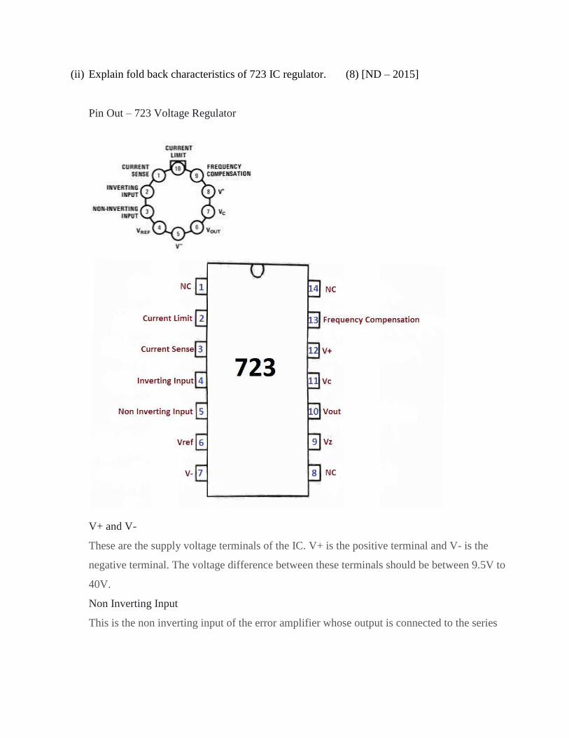
Pin Out – 723 Voltage Regulator
V+ and V-
These are the supply voltage terminals of the IC. V+ is the positive terminal and V- is the
negative terminal. The voltage difference between these terminals should be between 9.5V to
40V.
Non Inverting Input
This is the non inverting input of the error amplifier whose output is connected to the series
pass transistor. We usually give reference voltage or a portion of it to the non inverting input.
Inverting Input
This is the inverting input of the error amplifier whose output is connected to the series pass
transistor. We usually give output voltage or a portion of it to the inverting input. This makes
the output voltage constant.
Vref
It is the reference voltage output of the IC. It is the output of voltage reference amplifier. Its
output voltage is about 7.15V.
Vout
It is the output terminal of the IC. Usually output voltage ranges from 2 to 37V. This pin can
provide up to 150mA current.
Current Limit
It is the base input of the current limiter transistor. This pin is used for current limiting or
current fold back applications.
Current Sense
This is the emitter of current limiting transistor. This terminal is used with current limiting
and current fold-back applications.
Vc
This is the collector input of the series pass transistor. It is usually directly connected to the
positive supply voltage if an external transistor is not used.
Freq. Comp
Frequency Compensation : This pin is used to connect a capacitor which bypasses high
frequency noises. It is the output of error amplifier. The capacitor is connected between this
pin and inverting input of the error amplifier.
Or
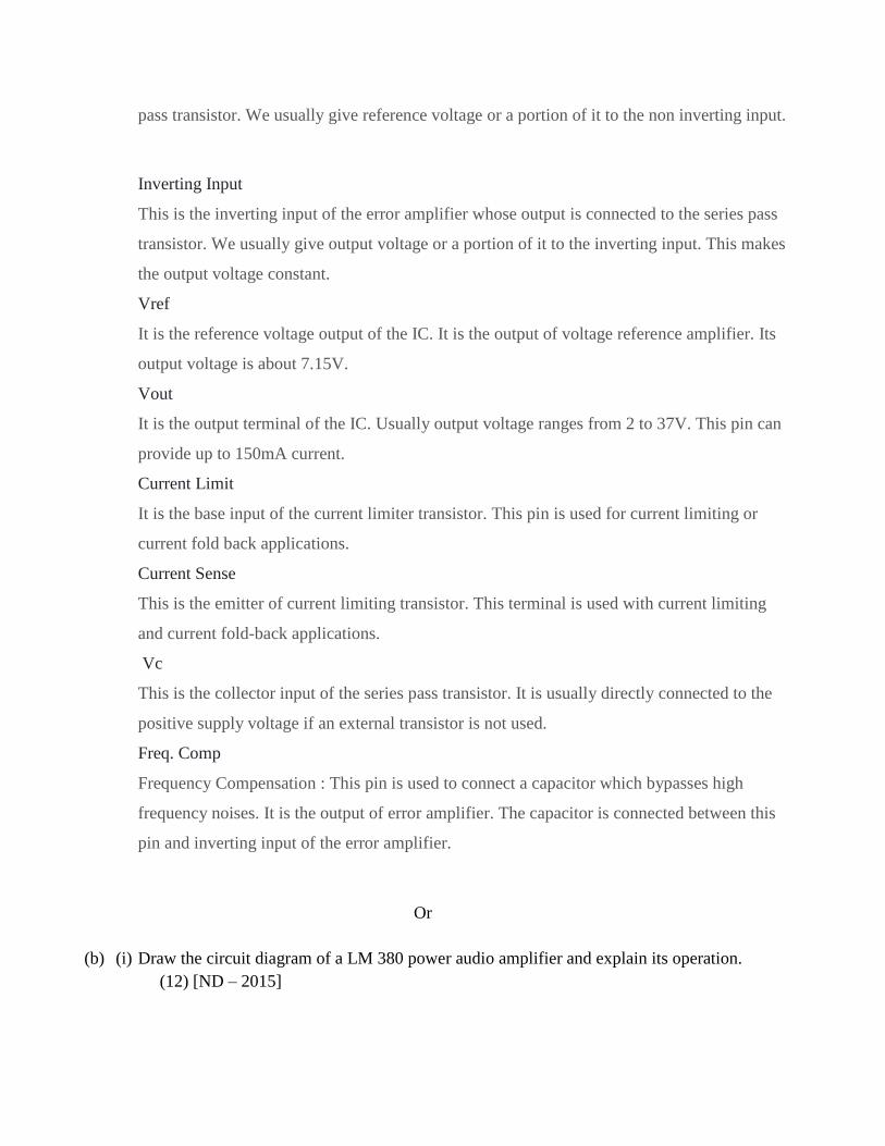
(b) (i) Draw the circuit diagram of a LM 380 power audio amplifier and explain its operation.
(12) [ND – 2015]

With a neat diagram explain the operation of LM 380 power amplifier
(8)(A/M 15)

The LM380 is a power audio amplifier for consumer applications. In order to hold
system cost to a minimum, gain is internally fixed at 34 dB. A unique input stage allows
ground referenced input signals. The output automatically self-centers to one-half the supply
voltage.
The output is short circuit proof with internal thermal limiting. The package outline
is standard dual-in-line. The LM380N uses a copper lead frame. The center three pins on
either side comprise a heat sink. This makes the device easy to use in standard PC layouts.
Uses include simple phonograph amplifiers, intercoms, line drivers, teaching
machine outputs, alarms, ultrasonic drivers, TV sound systems, AM-FM radio, small servo
drivers, power converters, etc.
Features
Wide Supply Voltage Range: 10V-22V
Low Quiescent Power Drain: 0.13W (VS= 18V)
Voltage Gain Fixed at 50
High Peak Current Capability: 1.3A
Input Referenced to GND
High Input Impedance: 150kΩ
Low Distortion
Quiescent Output Voltage is at One-Half of the Supply Voltage
Standard Dual-In-Line Package
(ii) What are the applications of LM 380 power amplifier? (4) [ND – 2015]
The following figure shows the simplest and most basic application of the ECG704 or
LM380 as an audio power amplifier.
This amplifier requires very few external components (and absolutely no 10 kΩ
resistors!). Although the gain of the LM380 is internally fixed at 50, it can be changed with
the use of external components. In the present configuration, variable gains up to 50 are
obtained with the use of the potentiometer across the two input terminals. Note the polarities
of the electrolytic capacitors having values greater than 1 µF.
Most electrolytic capacitors are polarized and may catastrophically fail if voltage is
incorrectly applied. This is because a reverse-bias voltage above 1 to 1.5 V will destroy the
center layer of dielectric material via electrochemical reduction.
12. (a) (i) Explain the working of series voltage regulator.
(8)(A/M 15)
A voltage regulator is a voltage stabilizer that is designed to automatically stabilize a
constant voltage level. A voltage regulator circuit is also used to change or stabilize the
voltage level according to the necessity of the circuit. Thus, a voltage regulator is used for two
reasons:-
1. To regulate or vary the output voltage of the circuit.
2. To keep the output voltage constant at the desired value in-spite of variations in the
supply voltage or in the load current.
3.
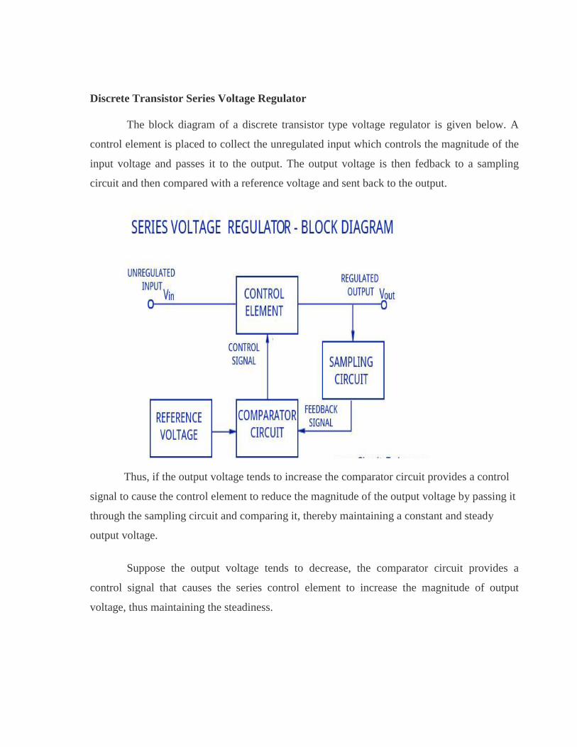
Discrete Transistor Series Voltage Regulator
The block diagram of a discrete transistor type voltage regulator is given below. A
control element is placed to collect the unregulated input which controls the magnitude of the
input voltage and passes it to the output. The output voltage is then fedback to a sampling
circuit and then compared with a reference voltage and sent back to the output.
Thus, if the output voltage tends to increase the comparator circuit provides a control
signal to cause the control element to reduce the magnitude of the output voltage by passing it
through the sampling circuit and comparing it, thereby maintaining a constant and steady
output voltage.
Suppose the output voltage tends to decrease, the comparator circuit provides a
control signal that causes the series control element to increase the magnitude of output
voltage, thus maintaining the steadiness.

(ii) Explain the working principle of IC 8038 function generator
(8)(A/M 15)
The ICL8038 is a function generator chip, capable of generating triangular, square ,
sine, pulse and saw tooth waveforms . From these since, square & triangular wave forms can
be made simultaneously. There is an option to control the parameters like frequency, duty
cycle and distortion of these functions. This is the best function generator circuit for a
beginner to start with and is of course a must on the work bench of an electronics hobbyist.
The circuit here is designed to produce waveforms from 20Hz to 20 kHz. The ICL 8038 has to
be operated from a dual power supply
The circuit needs a dual power supply. A +15 -15 power supply as shown in the
circuit is enough for the purpose.
The frequency of the output wave form can be adjusted using R7.It must be a 100K
Log POT.
The duty cycle can be adjusted using R3, a 1K POT.
The distortion of the wave form can be adjusted using R5, a 100K POT.
Square, triangle & sine waveforms can be obtained simultaneously at pins 9,3,2
respectively.
or
(b) (i) What is the principle of switch-mode power supplies? Discuss its advantages and
disadvantages. (8)(A/M 15)
A switched-mode power supply (switching-mode power supply, switch-mode power
supply, switched power supply, SMPS, or switcher) is an electronic power supply that
incorporates a switching regulator to convert electrical power efficiently. Like other power
supplies, an SMPS transfers power from a DC or AC source (often mains power) to DC loads,
such as a personal computer, while converting voltage and current characteristics. Unlike
a linear power supply, the pass transistor of a switching-mode supply continually switches
between low-dissipation, full-on and full-off states, and spends very little time in the high
dissipation transitions, which minimizes wasted energy. Ideally, a switched-mode power
supply dissipates no power. Voltage regulation is achieved by varying the ratio of on-to-off
time. In contrast, a linear power supply regulates the output voltage by continually dissipating
power in the pass transistor. This higher power conversion efficiency is an important
advantage of a switched-mode power supply. Switched-mode power supplies may also be
substantially smaller and lighter than a linear supply due to the smaller transformer size and
weight.
Switching regulators are used as replacements for linear regulators when higher
efficiency, smaller size or lighter weight is required. They are, however, more complicated;
their switching currents can cause electrical noise problems if not carefully suppressed, and

simple designs may have a poor power factor.
A linear regulator provides the desired output voltage by dissipating excess power
in ohmic losses (e.g., in a resistor or in the collector–emitter region of a pass transistor in its
active mode). A linear regulator regulates either output voltage or current by dissipating the
excess electric power in the form of heat, and hence its maximum power efficiency is voltage-
out/voltage-in since the volt difference is wasted.
In contrast, a switched-mode power supply regulates either output voltage or current
by switching ideal storage elements, like inductors and capacitors, into and out of different
electrical configurations. Ideal switching elements (e.g., transistors operated outside of their
active mode) have no resistance when "closed" and carry no current when "open", and so the
converters can theoretically operate with 100% efficiency (i.e., all input power is delivered to
the load; no power is wasted as dissipated heat).
The basic schematic of a boost converter.
For example, if a DC source, an inductor, a switch, and the corresponding electrical
ground are placed in series and the switch is driven by a square wave, the peak-to-peak
voltage of the waveform measured across the switch can exceed the input voltage from the
DC source. This is because the inductor responds to changes in current by inducing its own
voltage to counter the change in current, and this voltage adds to the source voltage while the
switch is open. If a diode-and-capacitor combination is placed in parallel to the switch, the
peak voltage can be stored in the capacitor, and the capacitor can be used as a DC source with
an output voltage greater than the DC voltage driving the circuit. This boost converter acts
like a step-up transformer for DC signals. A buck–boost converter works in a similar manner,
but yields an output voltage which is opposite in polarity to the input voltage. Other buck
circuits exist to boost the average output current with a reduction of voltage.
In a SMPS, the output current flow depends on the input power signal, the storage
elements and circuit topologies used, and also on the pattern used (e.g., pulse-width

modulation with an adjustable duty cycle) to drive the switching elements. The spectral
density of these switching waveforms has energy concentrated at relatively high frequencies.
As such, switching transients and ripple introduced onto the output waveforms can be filtered
with a small LC filter
ADVANTAGES AND DISADVANTAGES
The main advantage of the switching power supply is greater efficiency than linear
regulators because the switching transistor dissipates little power when acting as a switch.
Other advantages include smaller size and lighter weight from the elimination of
heavy line-frequency transformers, and comparable heat generation. Standby power loss is
often much less than transformers.
Disadvantages include greater complexity, the generation of high-amplitude, high-
frequency energy that the low-pass filter must block to avoid electromagnetic
interference (EMI), a ripple voltage at the switching frequency and the harmonic
frequencies thereof.
Very low cost SMPSs may couple electrical switching noise back onto the mains
power line, causing interference with A/V equipment connected to the same phase. Non-
power-factor-corrected SMPSs also cause harmonic distortion.
13. (a) (i) Explain the operation of switching regulator. Give its advantages (16)(M/J 16)
A switching regulator rapidly switches a series device on and off. The switch’s duty
cycle sets the amount of charge transferred to the load. This is controlled by a feedback
mechanism similar to that of a linear regulator. Switching regulators are efficient because the
series element is either fully conducting or switched off because it dissipates almost no
power. Switching regulators are able to generate output voltages that are higher than the input
voltage or of opposite polarity, unlike linear regulators.
Types of Switching Regulators
There are many different kinds of switching regulators. At Future Electronics we stock
many of the most common types categorized by topology, maximum switching frequency,
maximum output current, packaging type and input voltage. The parametric filters on our
website can help refine your search results depending on the required specifications.
The most common values for maximum switching frequency are 300 kHz, 1 MHz,
1.5 MHz and 4 MHz. We also carry switching regulators with maximum switching frequency
up to 2.5 GHz. Maximum output current can have a range from -5 mA to 30 A, with the most
common chips having a maximum output current of 1.5 A, 2 A or 3 A.
Switching Regulators from Future Electronics
Future Electronics has a full programmable switching regulator chip selection from
several manufacturers that can be used for switching regulator ic (integrated circuit),
switching voltage regulator, inverting switching regulator, 5v switching regulator, switching
power regulator or any other device that may require a switching regulator. Simply choose
from the switching regulator technical attributes below and your search results will quickly be
narrowed in order to match your specific switching regulator application needs.
If you have a preferred brand, we deal with several semiconductor chip
manufacturers such as Micrel Semiconductor, Microchip, ON Semiconductor, ROHM
Semiconductor or STMicroelectronics, among others. You can easily refine your switching
regulator product search results by clicking your preferred switching regulator brand below
from our list of manufacturers.
Applications for Switching Regulators:
Switching regulators and switched-mode power supply units are often found in
domestic products such as personal computers and have universal inputs, meaning they can
accept power from main supplies worldwide. Switch-mode power supplies can tolerate a wide
range of voltages and power frequencies. Switching regulators are also used for DC to DC
conversion.

As we see can see, the switching regulator is really nothing more than just a simple
switch. This switch goes on and off at a fixed rate usually between 50Khz to 100Khz as set by
the circuit.
The time that the switch remains closed during each switch cycle is varied to
maintain a constant output voltage. Notice that the primary filter capacitor is on the output of
the regulator and not the input. As is apparent, the switching regulator is much more efficient
than the linear regulator achieving efficiencies as high as 80% to 95% in some circuits. The
obvious result is smaller heat sinks, less heat and smaller overall size of the power supply.
The previous diagram is really an over simplification of a switching regulator circuit.
An actual switching regulator circuit more closely resembles the circuit below:
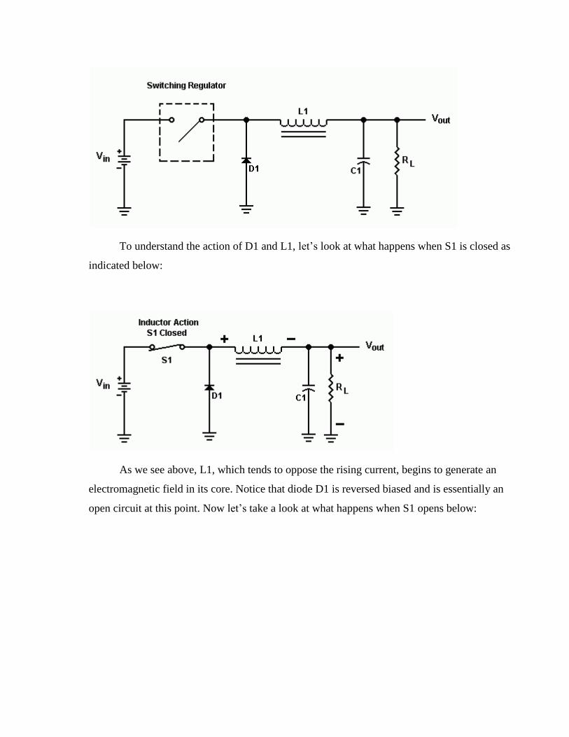
To understand the action of D1 and L1, let’s look at what happens when S1 is closed as
indicated below:
As we see above, L1, which tends to oppose the rising current, begins to generate an
electromagnetic field in its core. Notice that diode D1 is reversed biased and is essentially an
open circuit at this point. Now let’s take a look at what happens when S1 opens below:
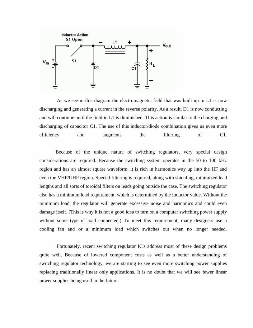
As we see in this diagram the electromagnetic field that was built up in L1 is now
discharging and generating a current in the reverse polarity. As a result, D1 is now conducting
and will continue until the field in L1 is diminished. This action is similar to the charging and
discharging of capacitor C1. The use of this inductor/diode combination gives us even more
efficiency and augments the filtering of C1.
Because of the unique nature of switching regulators, very special design
considerations are required. Because the switching system operates in the 50 to 100 kHz
region and has an almost square waveform, it is rich in harmonics way up into the HF and
even the VHF/UHF region. Special filtering is required, along with shielding, minimized lead
lengths and all sorts of toroidal filters on leads going outside the case. The switching regulator
also has a minimum load requirement, which is determined by the inductor value. Without the
minimum load, the regulator will generate excessive noise and harmonics and could even
damage itself. (This is why it is not a good idea to turn on a computer switching power supply
without some type of load connected.) To meet this requirement, many designers use a
cooling fan and or a minimum load which switches out when no longer needed.
Fortunately, recent switching regulator IC's address most of these design problems
quite well. Because of lowered component costs as well as a better understanding of
switching regulator technology, we are starting to see even more switching power supplies
replacing traditionally linear only applications. It is no doubt that we will see fewer linear
power supplies being used in the future.
or
(ii) With neat diagram, explain the working of step down switching regulator.(16) (N/D 14)
With power being a key parameter in many designs, step down or "buck" regulators
are widely used.
Although a resistor would enable voltage to be dropped, power is lost, and in
applications such as the many battery powered items used today, power consumption is a
crucial element.
As a result step down switch mode converters or as they are more commonly termed,
buck regulators are widely used.
Linear step down
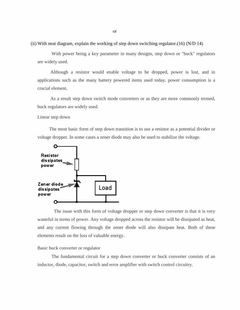
The most basic form of step down transition is to use a resistor as a potential divider or
voltage dropper. In some cases a zener diode may also be used to stabilize the voltage.
The issue with this form of voltage dropper or step down converter is that it is very
wasteful in terms of power. Any voltage dropped across the resistor will be dissipated as heat,
and any current flowing through the zener diode will also dissipate heat. Both of these
elements result on the loss of valuable energy.
Basic buck converter or regulator
The fundamental circuit for a step down converter or buck converter consists of an
inductor, diode, capacitor, switch and error amplifier with switch control circuitry.

The circuit for the buck regulator operates by varying the amount of time in which
inductor receives energy from the source.
In the basic block diagram the operation of the buck converter or buck regulator can
be seen that the output voltage appearing across the load is sensed by the sense / error
amplifier and an error voltage is generated that controls the switch.
Typically the switch is controlled by a pulse width modulator, the switch remaining on
of longer as more current is drawn by the load and the voltage tends to drop and often there is
a fixed frequency oscillator to drive the switching.
Buck converter operation
When the switch in the buck regulator is on, the voltage that appears across the
inductor is Vin - Vout. Using the inductor equations, the current in the inductor will rise at a
rate of (Vin-Vout)/L. At this time the diode D is reverse biased and does not conduct.

When the switch opens, current must still flow as the inductor works to keep the
same current flowing. As a result current still flows through the inductor and into the load.
The diode, D then forms the return path with a current I diode equal to I out flowing through
it.
With the switch open, the polarity of the voltage across the inductor has reversed and
therefore the current through the inductor decreases with a slope equal to - Vout /L.
The step down, buck converter circuit can be further explained by examining the
current waveforms at different times during the overall cycle.
In the diagram of the current waveforms for the buck converter / switching
regulator, it can be seen that the inductor current is the sum of the diode and input / switch
current. Current either flows through the switch or the diode.
It is also worth noting that the average input current is less than the average output
current. This is to be expected because the buck converter circuit is very efficient and the
input voltage is greater than the output voltage. Assuming a perfect circuit, then power in
would equal power out, i.e. Vin ⋅ In = Vout ⋅ Iout. While in a real circuit there will be some
losses, efficiency levels greater than 85% are to be expected for a well-designed circuit.
It will also be seen that there is a smoothing capacitor placed on the output. This
serves to ensure that the voltage does not vary appreciable, especially during and switch
transition times. It will also be required to smooth any switching spikes that occur.
Regulator input and output filtering
A key aspect of switch mode power supply regulators is the input and output filtering.
This is a particular issue because of the switching that occurs at the input.
In reality ripple voltage on the output is dependent not only on the output smoothing,
but more importantly on an input filter capacitor.