ee 459/500 hdl based digital design with programmable ... · 1 1 ee 459/500 – hdl based digital...
TRANSCRIPT

1
1
EE 459/500 – HDL Based Digital
Design with Programmable Logic
Lecture 15
Memories
Overview
Introduction
Memories
• Read Only Memories
• Random Access Memories
• FIFOs
2
2
3
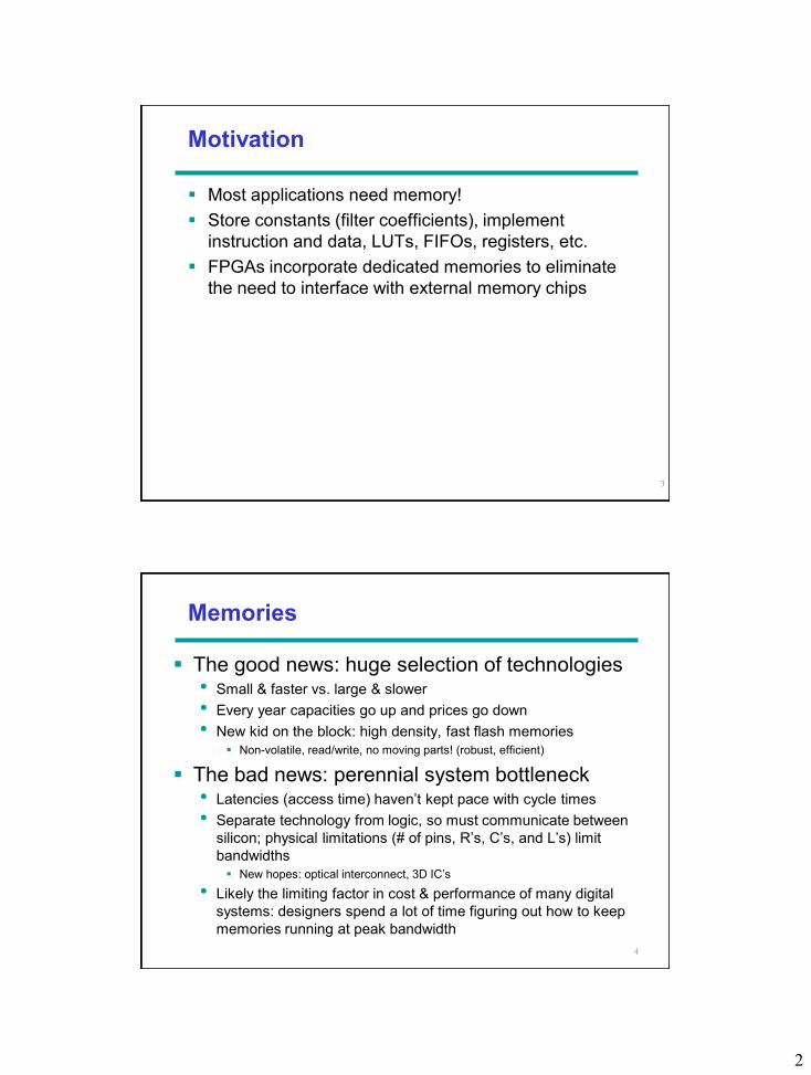
Motivation
Most applications need memory!
Store constants (filter coefficients), implement
instruction and data, LUTs, FIFOs, registers, etc.
FPGAs incorporate dedicated memories to eliminate
the need to interface with external memory chips
Memories
The good news: huge selection of technologies • Small & faster vs. large & slower
• Every year capacities go up and prices go down
• New kid on the block: high density, fast flash memories
Non-volatile, read/write, no moving parts! (robust, efficient)
The bad news: perennial system bottleneck • Latencies (access time) haven’t kept pace with cycle times
• Separate technology from logic, so must communicate between
silicon; physical limitations (# of pins, R’s, C’s, and L’s) limit
bandwidths
New hopes: optical interconnect, 3D IC’s
• Likely the limiting factor in cost & performance of many digital
systems: designers spend a lot of time figuring out how to keep
memories running at peak bandwidth
4

3
Memories classification Read-Write Memory Read-Only Memory
Volatile Memory Non-volatile
Memory
Mask-Programmed ROM (PROM)
(nonvolatile)
Random Access Sequential Access
EPROM
EEPROM
FLASH SRAM
DRAM
FIFO
LIFO
Shift Register
CAM
5
Key Design Metrics:
1.Memory Density (number of bits/mm2) and Size
2.Access Time (time to read or write) and Throughput
3.Power Dissipation
Volatile: need electrical power
Nonvolatile: magnetic disk, retains its stored information after the removal of power
Random access: memory locations can be read or written in a random order
EPROM: erasable programmable read-only memory
EEPROM: electrically erasable programmable read-only memory
FLASH: memory stick, USB disk
Access pattern: sequential access: (video memory streaming) first-in-first-out (buffer), last-in-
first-out (stack), shift register, content-addressable memory
Static vs. Dynamic: dynamic needs periodic refresh but is simpler, higher density
Basic memory system
L address lines are decoded to address 2L words of memory
Each word is M bits
Read and Write are single control lines defining the simplest memory operations
6
Data Input Lines
L address lines
Read
Write
Data Output Lines
L
1
1
M
M
Memory
Array
2L Words
M Bits per Word

4
7
Memory Array Architecture
Memory Operation Timing - Read
Most basic memories are asynchronous • Storage in latches/flip-flops or electrical charge storage elements (C’s)
• No clock
• Controlled by control inputs and address, which are controlled by CPU and synchronized by its own clock
Timing of signal changes/data observation is critical to operation
Read cycle: the access time, the maximum time from the application of the address to the appearance of the data at the Data output
Read cycle
Clock
Address
Memory enable
Read/ Write
Data output
20 ns
T1 T2 T3 T4 T1
Address valid
65 ns
Data valid
8

5
Memory Operation Timing - Write
Write cycle: the maximum time from the application of the address to the completion of all internal operations required to store a word
Critical times measured with respect to edges of write pulse (1-0-1): • Address must be established at least a specified time before 1-0 and held for at least
a specified time after 0-1 to avoid disturbing stored contents of other addresses
• Data must be established at least a specified time before 0-1 and held for at least a specified time after 0-1 to write correctly
Write cycle
Clock
Address
Memory enable
Read/ Write
Data input
20 ns
T1 T2 T3 T4 T1
Address valid
Data valid
75 ns
9
10
Overview
Motivation
Memories
• Read Only Memories
• Random Access Memories
• FIFOs

6
Read Only Memories (ROMs)
ROM modeling: ROMs are usually modeled in VHDL
with an array of array object
Signal-Based Declaration VHDL Coding Example
type rom_type is array (0 to 127) of std_logic_vector (19 downto 0);
signal ROM : rom_type:= (
X"0200A", X"00300", X"08101", X"04000", X"08601", X"0233A", X"00300", X"08602",
X"02310", X"0203B", X"08300", X"04002", X"08201", X"00500", X"04001", X"02500",
(…)
X"04078", X"01110", X"02500", X"02500", X"0030D", X"02341", X"08201", X"0410D"
);
Arrays in VHDL
type WORD16 is array (15 downto 0) of bit;
signal DATA_WORD: WORD16; -- a 16-bit register
subtype WORD8 is STD_LOGIC_VECTOR (7 downto 0);
type TAB12 is array (11 downto 0) of WORD8;
type TAB03 is array (2 downto 0) of TAB12;
You can also declare an array as a matrix:
subtype TAB13 is array (7 downto 0, 4 downto 0) of
STD_LOGIC_VECTOR (8 downto 0);
12

7
Examples
subtype WORD8 is STD_LOGIC_VECTOR (7 downto 0);
type TAB05 is array (4 downto 0) of WORD8;
type TAB03 is array (2 downto 0) of TAB05;
signal WORD_A : WORD8;
signal TAB_A, TAB_B : TAB05;
signal TAB_C, TAB_D : TAB03;
constant CNST_A : TAB03 := (
("00000000","01000001","01000010","10000011","00001100"),
("00100000","00100001","00101010","10100011","00101100"),
("01000010","01000010","01000100","01000111","01000100"));
TAB_A <= TAB_B; TAB_C <= TAB_D; TAB_C <= CNST_A;
TAB_A (5) <= WORD_A; TAB_C (1) <= TAB_A;
TAB_A (5) (0) <= ’1’; TAB_C (2) (5) (0) <= ’0’;
TAB_A (4 downto 1) <= TAB_B (3 downto 0);
13
Describing ROM with a Case Statement
ARCHITECTURE behav OF rom8x4 IS
BEGIN
PROCESS(addr)
BEGIN
CASE addr IS
when "000" => q <= "0001";
when "001" => q <= "0000";
when "010" => q <= "0111";
when "011" => q <= "1101";
when "100" => q <= "1000";
when "101" => q <= "1100";
when "110" => q <= "0110";
when "111" => q <= "1011";
when others => NULL;
END case;
END process;
END behav;
ENTITY rom8x4 IS
PORT (
addr: in std_logic_vector(2 downto 0);
q: out std_logic_vector(3 downto 0));
END rom8x4;
14
8
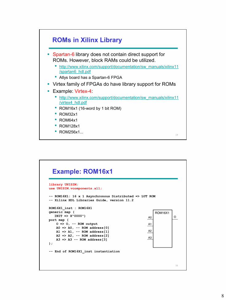
ROMs in Xilinx Library
Spartan-6 library does not contain direct support for
ROMs. However, block RAMs could be utilized.
• http://www.xilinx.com/support/documentation/sw_manuals/xilinx11
/spartan6_hdl.pdf
• Atlys board has a Spartan-6 FPGA
Virtex family of FPGAs do have library support for ROMs
Example: Virtex-4:
• http://www.xilinx.com/support/documentation/sw_manuals/xilinx11
/virtex4_hdl.pdf
• ROM16x1 (16-word by 1 bit ROM)
• ROM32x1
• ROM64x1
• ROM128x1
• ROM256x1... 15
Example: ROM16x1
library UNISIM;
use UNISIM.vcomponents.all;
-- ROM16X1: 16 x 1 Asynchronous Distributed => LUT ROM
-- Xilinx HDL Libraries Guide, version 11.2
ROM16X1_inst : ROM16X1
generic map (
INIT => X"0000")
port map (
O => O, -- ROM output
A0 => A0, -- ROM address[0]
A1 => A1, -- ROM address[1]
A2 => A2, -- ROM address[2]
A3 => A3 -- ROM address[3]
);
-- End of ROM16X1_inst instantiation
16

9
How do we use ROMs
architecture beh of my_example_rom is
signal ABUS : std_logic_vector(3 downto 0);
signal DBUS : std_logic_vector(1 downto 0);
begin
bit0 : ROM16X1
generic map (INIT => “1010 1110 0001 0001” )
port map (O => DBUS(0), A0 => ABUS(0),
A1 => ABUS(1), A2 => ABUS(2), A3 => ABUS(3) );
bit1 : ROM16X1
generic map (INIT => ”1101 1010 1111 0101”)
port map (O => DBUS(1), A0 => ABUS(0),
A1 => ABUS(1), A2 => ABUS(2), A3 => ABUS(3) );
rom_inc : process(CLK) is
begin
if (CLK’event and CLK=‘1’) then
ABUS <= ABUS + 1;
end if;
end process;
jump : process(DBUS) is
begin
if (DBUS=“11”) then
ABUS <= “0000”;
end if;
end;
end architecture; 17
18
Overview
Motivation
Memories
• Read Only Memories
• Random Access Memories
• FIFOs
10
19
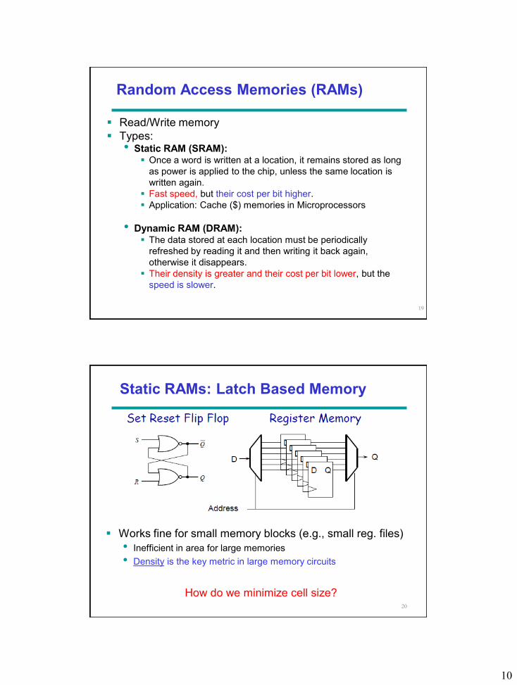
Random Access Memories (RAMs)
Read/Write memory
Types: • Static RAM (SRAM):
Once a word is written at a location, it remains stored as long
as power is applied to the chip, unless the same location is
written again.
Fast speed, but their cost per bit higher.
Application: Cache ($) memories in Microprocessors
• Dynamic RAM (DRAM): The data stored at each location must be periodically
refreshed by reading it and then writing it back again,
otherwise it disappears.
Their density is greater and their cost per bit lower, but the
speed is slower.
Static RAMs: Latch Based Memory
20
Works fine for small memory blocks (e.g., small reg. files)
• Inefficient in area for large memories
• Density is the key metric in large memory circuits
How do we minimize cell size?
11
21
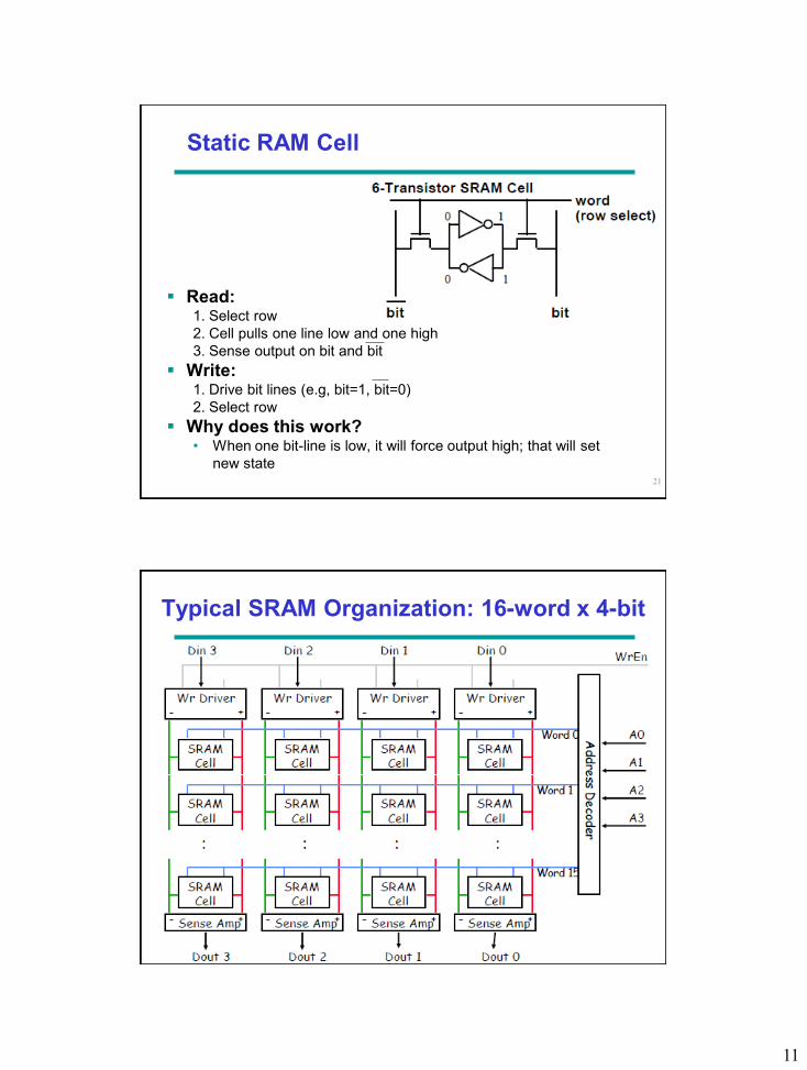
Static RAM Cell
Read: 1. Select row
2. Cell pulls one line low and one high
3. Sense output on bit and bit
Write: 1. Drive bit lines (e.g, bit=1, bit=0)
2. Select row
Why does this work? • When one bit-line is low, it will force output high; that will set
new state
Typical SRAM Organization: 16-word x 4-bit

12
Logic Diagram of a Typical SRAM
Write Enable is usually active low (WE_L)
Din and Dout are combined to save pins:
A new control signal, Output Enable (OE_L) • WE_L is asserted (Low), OE_L is unasserted (High)
D serves as the data input pin
• WE_L is unasserted (High), OE_L is asserted (Low)
D is the data output pin
• Neither WE_L and OE_L are asserted?
Chip is disconnected
• Never both asserted!
Typical SRAM Timing
24

13
25
Making Larger Memories
We can make larger memories from smaller ones by using the decoded higher order address bits to control CS (chip select) lines, tying all address, data, and R/W lines in parallel
A 16-Word by1-Bit memory constructed using 4-Word by 1-Bit memory
D3
S1
S0
D2
D1
D0
Decoder
R/W
A2
A3
A1
A0
Data In
Data Out
R/WCS
A0A1 D-In
D-Out
R/WCS
A0A1 D-In
D-Out
R/WCS
A0A1 D-In
D-Out
R/WCS
A0A1 D-In
D-Out
26
Making Wider Memories
Tie the address and control
lines in parallel and keep
the data lines separate
Example: make a 4-word by
4-bit memory from 4, 4-
word by 1-bit memories
Note: Both 16x1 and 4x4
memories take 4-chips
and hold 16 bits of data R/W
A1A0
Data In
Data Out
R/WCS
A0A1 D-In
D-Out
R/WCS
A0A1 D-In
D-Out
R/WCS
A0A1 D-In
D-Out
R/WCS
A0A1 D-In
D-Out
CS
3 2 1 0
3 2 1 0

14
RAMs in Xilinx Library
Static Block RAMs
Single port • RAM32X1S, RAM64X1S, ...
Dual port • RAM64X1D, RAM128X1D, ...
27
• The difference between single port RAM and dual port RAM is that
single port RAM can be accessed at one address at one time, thus you
can read/write only one memory cell during each clock cycle. Dual port
RAM has ability to simultaneously read and write different memory
cells at different addresses.
• Single port uses a 6 transistor basic RAM cell, while the dual port RAM
cell uses 8 transistor cell for memory.
28
Block RAMs (BRAMs)
A Block RAM is a dedicated (cannot be used to implement
other functions like digital logic) two port memory
The Block RAM in Spartan-6 FPGAs stores up to 18K bits
of data and can be configured as:
• Two independent 9 Kb RAMs
• One 18 Kb RAM
Write and Read are synchronous operations
The two ports are symmetrical and totally independent,
sharing only the stored data.
Embedded dual- or single-port RAM modules, ROM
modules, synchronous FIFOs, and data-width converters
are easily implemented using the Xilinx CORE Generator
block memory modules

15
Difference between Distributed and Block RAMs
Distributed RAM = parallel array of large # of elements
distributed RAM is ideal for small sized memories.
For large memories, extra wiring delays
Use block RAM for large sized memories and
distributed RAM for small sized memories or FIFO's
WRITE operation is synchronous in both
READ operation:
• Distributed RAM: asynchronous (data is read from memory
as soon as the address is given, doesn't wait for the clock
edge)
• Block RAM: synchronous
Example: RAM32X1S
library UNISIM;
use UNISIM.vcomponents.all;
-- RAM32X1S: 32 x 1 posedge write distributed => LUT RAM
-- All FPGA
-- Xilinx HDL Libraries Guide, version 11.2
RAM32X1S_inst : RAM32X1S
generic map (
INIT => X"00000000")
port map (
O => O, -- RAM output
A0 => A0, -- RAM address[0] input
A1 => A1, -- RAM address[1] input
A2 => A2, -- RAM address[2] input
A3 => A3, -- RAM address[3] input
A4 => A4, -- RAM address[4] input
D => D, -- RAM data input
WCLK => WCLK, -- Write clock input
WE => WE -- Write enable input
);
-- End of RAM32X1S_inst instantiation 30

16
31
True dual-port 18 Kb block RAM dual-port
memories
See “Spartan-6 FPGA Block RAM Resources” for timing diagrams
• http://www.xilinx.com/support/documentation/user_guides/ug383.pdf
• http://www.xilinx.com/support/documentation/data_sheets/ds160.pdf
How to tell XST which type of RAM you want to
use?
XST (Xilinx Synthesis Tool) may implement a declared
RAM as either
• block RAM
• distributed RAM
You can force the implementation style to use block RAM
or distributed RAM resources
Done using the ram_style constraint
Before the begin statement in the architecture section:
• attribute ram_style: string;
• attribute ram_style of ram: signal is “distributed“;
• Here ram is the signal name. Change "distributed" to "block" to
force XST to use block RAM resources. Default value of the
attribute ram_style is "auto".

17
library IEEE;
use IEEE.STD_LOGIC_1164.ALL;
entity ram_example is
port ( Clk : in std_logic;
address : in integer;
we : in std_logic;
data_i : in std_logic_vector(7 downto 0);
data_o : out std_logic_vector(7 downto 0)
);
end ram_example;
architecture Behavioral of ram_example is
--Declaration of type and signal of a 256 element RAM; each word is 8 bit wide.
type ram_t is array (0 to 255) of std_logic_vector(7 downto 0);
signal ram : ram_t := (others => (others => '0'));
attribute ram_style: string;
attribute ram_style of ram : signal is “distributed“;
begin
--process for read and write operation.
PROCESS(Clk)
BEGIN
if(rising_edge(Clk)) then
if(we='1') then
ram(address) <= data_i;
end if;
data_o <= ram(address);
end if;
END PROCESS;
end Behavioral;
Example
Block RAM Applications
The Xilinx CORE Generator program offers an
easy way to generate wider and deeper memory
structures using multiple Block RAM instances
It outputs VHDL or Verilog instantiation
templates and simulation models
See Lab#5 for details

18
Creating BRAMs with Core Generator
Using the result in your VHDL project
ENTITY my_bram8x8 IS
PORT (
clka : IN STD_LOGIC;
wea : IN STD_LOGIC_VECTOR(0 DOWNTO 0);
addra : IN STD_LOGIC_VECTOR(2 DOWNTO 0);
dina : IN STD_LOGIC_VECTOR(7 DOWNTO 0);
douta : OUT STD_LOGIC_VECTOR(7 DOWNTO 0)
);
END my_bram8x8;
Use to instantiate components:
memory2 : my_bram8x8 port map (clka=>clk_1Hz, wea=>wea_null,
addra=>my_addr_counter, dina=>dina_null,
douta=>dout_bram8x8);

19
.coe file format (used during Core Generator
usage)
memory_initialization_radix=2;
memory_initialization_vector=
10000000,
01000000,
00100000,
00010000,
00001000,
00000100,
00000010,
00000001;
Dynamic RAM (DRAM)
Basic Principle: Storage of information on capacitors
Charge and discharge of capacitor to change stored value
Use of transistor as “switch” to: • Store charges
• Charge or discharge
You will normally not find DRAMs in FPGAs

20
Overview
Motivation
Memories
• Read Only Memories
• Random Access Memories
• FIFOs
First-in-first-out (FIFO) Memory
40
Used to implement queues.
These find common use in
computers and communication
circuits.
Generally, used for rate matching
data producer and consumer:
Producer can perform many writes
without consumer performing any
reads (or vice versa). However,
because of finite buffer size, on
average, need equal number of
reads and writes.
Typical uses:
• Interfacing I/O devices. Example
network interface. Data bursts from
network, then processor bursts to
memory buffer (or reads one word
at a time from interface).
Operations not synchronized.
• Example: Audio output. Processor
produces output samples in bursts
(during process swap-in time).
Audio DAC clocks it out at constant
sample rate.
stating state
after write
after read

21
Address pointers are used internally to keep
next write position and next read position into
a dual-port memory.
If pointers equal after write FULL:
If pointers equal after read EMPTY:
FIFO Interfaces
41
After write or read operation,
FULL and EMPTY indicate status
of buffer.
Used by external logic to
control own reading from or
writing to the buffer.
FIFO resets to EMPTY state.
HALF FULL (or other indicator
of partial fullness) is optional.
DIN
DOUT
WE
RE
EMPTY
FULL
HALF FULL
RST CLK
FIFO
write ptr
read ptr
write ptr read ptr
write ptr read ptr
FIFO Implementation
42
FIFOs available in Xilinx library for
Virtex-4 and up devices
For Spartan-6 one could use
LogiCORE FIFO Generator?
See Lab#7 supplemental
WE RE equal EMPTYi FULLi
0 0 0 0 0
0 0 1 EMPTYi-1 FULLi-1
0 1 0 0 0
0 1 1 1 0
1 0 0 0 0
1 0 1 0 1
1 1 0 0 0
1 1 1 EMPTYi-1 FULLi-1
Assume, dual-port memory with asynchronous read, synchronous write.
Binary counter for each of read and write address. CEs controlled by WE and RE.
Equal comparator to see when pointers match.
Flip-flop each for FULL and EMPTY flags:

22
Summary
Memories are complex circuits and different
from random logic
Companies, like Xilinx, offer pre-designed cores
to help designers improve productivity
Always consult documentation of FPGAs to see
what types of memory blocks are available
Do not underestimate FIFOs
Timing issues are extremely important
References and Credits
Textbook
• Sections 3.2, 3.4, 6.6, 8.7, 8.8, and 11.2
Chapter 13 of Volnei A. Pedroni book
Chapter 9 of M. Morris Mano and Charles Kime book
Jan Rabaey book (on timing and clock issues)
MIT 6.111 slides
• http://web.mit.edu/6.111/www/f2011/handouts/L10.pdf
Berkeley CS150 slides
• http://www-inst.eecs.berkeley.edu/~cs150/fa07/Lectures/lec13-mem-sram.pdf
XST User Guide for Virtex-6, Spartan-6, and 7 Series Devices - ROMs
and ROM coding examples (page 247):
• http://www.xilinx.com/support/documentation/sw_manuals/xilinx13_1/xst_v6s6.pdf
Spartan-6 Libraries Guide for HDL Designs
http://www.xilinx.com/support/documentation/sw_manuals/xilinx11/spartan6_hdl.pdf
Spartan-6 FPGA Block RAM Resources
• http://www.xilinx.com/support/documentation/user_guides/ug383.pdf 44

23
45
Storage Cell • SR Latch
• Select input for control
• Dual Rail Data Inputs B and B
• Dual Rail Data Outputs C and C
Select
B
RAM cell
C
C
B
S
R
Q
Q
Appendix A:
Revisiting Static RAM Cell: SR latch based
SRAM Bit Slice
Represents all
circuitry that is
required for 2n 1-bit
words
• Multiple RAM cells
• Control Lines:
Word select i
– one for each word
Bit Select
• Data Lines:
Data in
Data out
WriteRead/
(a) Logic diagram
Select
S
R
Q
Q
B
RAM cell
C
C
B
Select
S
R
Q
Q
RAM cell
X
Word select 0
Word select 2
n - 1
Data in
Write logic
Read/ Write
Bit select
S
R
Q
Q
X
X
X
Data out Read logic
Read/Write logic
Data in
Data out
Read/ Write
Bit select
(b) Symbol
Word select 0
Word select 1
Word select 2 n
RAM cell
RAM cell
RAM cell
- 1
24
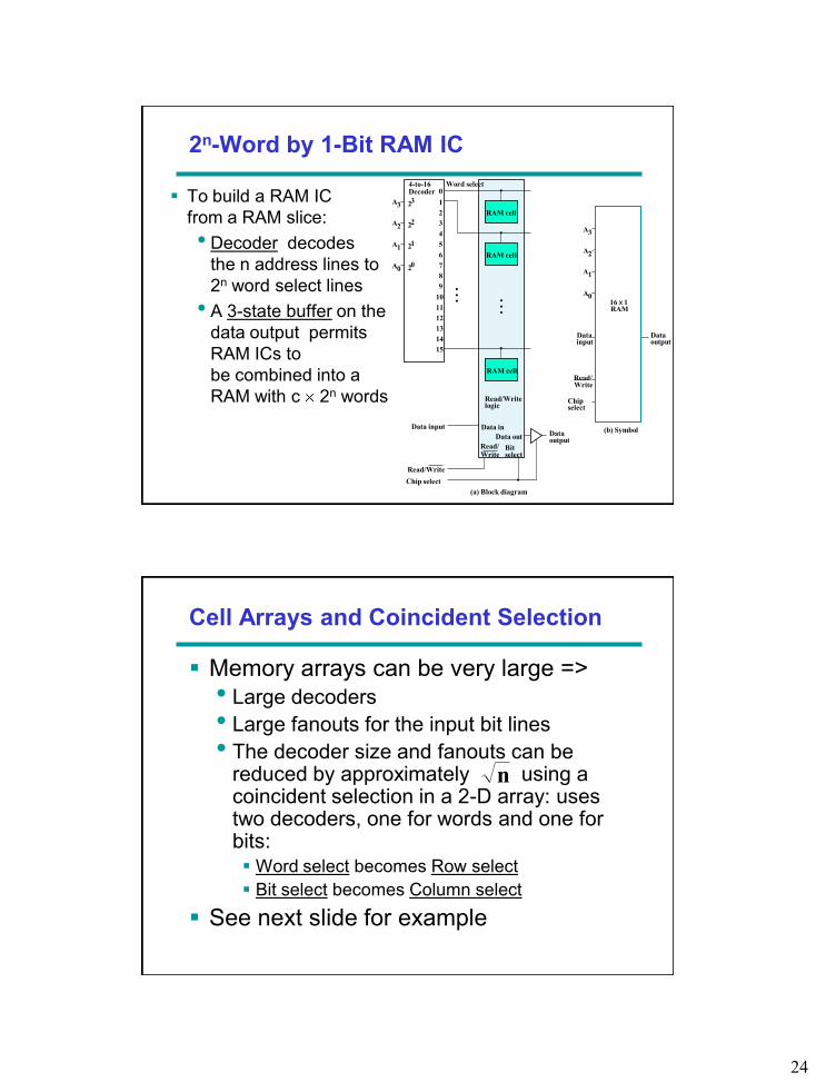
2n-Word by 1-Bit RAM IC
To build a RAM IC
from a RAM slice:
• Decoder decodes
the n address lines to
2n word select lines
• A 3-state buffer on the
data output permits
RAM ICs to
be combined into a
RAM with c 2n words Chip select
A 3
A 2
A 1
A 0
Data input
Data output
(b) Symbol
Read/ Write
16 x 1 RAM
Read/
Word select
Read/Write logic
Data in
Data out
Write
Bit select
(a) Block diagram
RAM cell
RAM cel l
RAM cell
Data input
Chip select
Read/Write
Data output
A 3
A 2
A 1
A 0
2 3
2 2
2 1
2 0
4-to-16
Decoder 0
1
2
3
4
5
6
7
8
9
10
11
12
13
14
15
Cell Arrays and Coincident Selection
Memory arrays can be very large =>
• Large decoders
• Large fanouts for the input bit lines
• The decoder size and fanouts can be reduced by approximately using a coincident selection in a 2-D array: uses two decoders, one for words and one for bits: Word select becomes Row select
Bit select becomes Column select
See next slide for example
n

25
Cell Arrays and Coincident Selection (Contd.)
A1 and A0 used for Row select
A3 and A2 for Column select
Data input
Read/Write
X X X
A 3 A 2
RAM cell 0
RAM cell 1
RAM cell 2
RAM cell 3
Read/Write logic
Data in
Data out
Read/ Write
Bit select
RAM cell 4
RAM cell 5
RAM cell 6
RAM cell 7
Read/Write logic
Data in
Data out
Read/ Write
Bit select
RAM cell 8
RAM cell 9
RAM cell 10
RAM cell 11
Read/Write logic
Data in
Data out
Read/ Write
Bit select
RAM cell 12
RAM cell 13
RAM cell 14
RAM cell 15
Read/Write logic
Data in
Data out
Read/ Write
Bit select
Column decoder
2-to-4 Decoder with enable
2 1 2
0
0 1
Column select
2
Enable
3
Chip select
Data output
Row select
Row decoder
A 0
A 1
X
2-to-4 Decoder
2 0
2 1
1
2
3
0